EP3568704B1 - Heterodyne rasterkraftmikroskopievorrichtung, -verfahren und lithographiesystem - Google Patents
Heterodyne rasterkraftmikroskopievorrichtung, -verfahren und lithographiesystem Download PDFInfo
- Publication number
- EP3568704B1 EP3568704B1 EP18702353.6A EP18702353A EP3568704B1 EP 3568704 B1 EP3568704 B1 EP 3568704B1 EP 18702353 A EP18702353 A EP 18702353A EP 3568704 B1 EP3568704 B1 EP 3568704B1
- Authority
- EP
- European Patent Office
- Prior art keywords
- probe tip
- probe
- acoustic
- frequency
- signal
- Prior art date
- Legal status (The legal status is an assumption and is not a legal conclusion. Google has not performed a legal analysis and makes no representation as to the accuracy of the status listed.)
- Active
Links
Images


Classifications
-
- G—PHYSICS
- G01—MEASURING; TESTING
- G01Q—SCANNING-PROBE TECHNIQUES OR APPARATUS; APPLICATIONS OF SCANNING-PROBE TECHNIQUES, e.g. SCANNING PROBE MICROSCOPY [SPM]
- G01Q60/00—Particular types of SPM [Scanning Probe Microscopy] or microscopes; Essential components thereof
- G01Q60/24—AFM [Atomic Force Microscopy] or apparatus therefor, e.g. AFM probes
- G01Q60/32—AC mode
-
- G—PHYSICS
- G01—MEASURING; TESTING
- G01Q—SCANNING-PROBE TECHNIQUES OR APPARATUS; APPLICATIONS OF SCANNING-PROBE TECHNIQUES, e.g. SCANNING PROBE MICROSCOPY [SPM]
- G01Q60/00—Particular types of SPM [Scanning Probe Microscopy] or microscopes; Essential components thereof
- G01Q60/24—AFM [Atomic Force Microscopy] or apparatus therefor, e.g. AFM probes
-
- G—PHYSICS
- G01—MEASURING; TESTING
- G01N—INVESTIGATING OR ANALYSING MATERIALS BY DETERMINING THEIR CHEMICAL OR PHYSICAL PROPERTIES
- G01N29/00—Investigating or analysing materials by the use of ultrasonic, sonic or infrasonic waves; Visualisation of the interior of objects by transmitting ultrasonic or sonic waves through the object
- G01N29/04—Analysing solids
- G01N29/06—Visualisation of the interior, e.g. acoustic microscopy
- G01N29/0654—Imaging
- G01N29/0681—Imaging by acoustic microscopy, e.g. scanning acoustic microscopy
-
- G—PHYSICS
- G01—MEASURING; TESTING
- G01N—INVESTIGATING OR ANALYSING MATERIALS BY DETERMINING THEIR CHEMICAL OR PHYSICAL PROPERTIES
- G01N29/00—Investigating or analysing materials by the use of ultrasonic, sonic or infrasonic waves; Visualisation of the interior of objects by transmitting ultrasonic or sonic waves through the object
- G01N29/22—Details, e.g. general constructional or apparatus details
- G01N29/26—Arrangements for orientation or scanning by relative movement of the head and the sensor
- G01N29/265—Arrangements for orientation or scanning by relative movement of the head and the sensor by moving the sensor relative to a stationary material
-
- G—PHYSICS
- G01—MEASURING; TESTING
- G01N—INVESTIGATING OR ANALYSING MATERIALS BY DETERMINING THEIR CHEMICAL OR PHYSICAL PROPERTIES
- G01N29/00—Investigating or analysing materials by the use of ultrasonic, sonic or infrasonic waves; Visualisation of the interior of objects by transmitting ultrasonic or sonic waves through the object
- G01N29/22—Details, e.g. general constructional or apparatus details
- G01N29/26—Arrangements for orientation or scanning by relative movement of the head and the sensor
- G01N29/27—Arrangements for orientation or scanning by relative movement of the head and the sensor by moving the material relative to a stationary sensor
-
- G—PHYSICS
- G01—MEASURING; TESTING
- G01N—INVESTIGATING OR ANALYSING MATERIALS BY DETERMINING THEIR CHEMICAL OR PHYSICAL PROPERTIES
- G01N29/00—Investigating or analysing materials by the use of ultrasonic, sonic or infrasonic waves; Visualisation of the interior of objects by transmitting ultrasonic or sonic waves through the object
- G01N29/22—Details, e.g. general constructional or apparatus details
- G01N29/26—Arrangements for orientation or scanning by relative movement of the head and the sensor
- G01N29/275—Arrangements for orientation or scanning by relative movement of the head and the sensor by moving both the sensor and the material
-
- G—PHYSICS
- G01—MEASURING; TESTING
- G01Q—SCANNING-PROBE TECHNIQUES OR APPARATUS; APPLICATIONS OF SCANNING-PROBE TECHNIQUES, e.g. SCANNING PROBE MICROSCOPY [SPM]
- G01Q20/00—Monitoring the movement or position of the probe
- G01Q20/02—Monitoring the movement or position of the probe by optical means
-
- G—PHYSICS
- G01—MEASURING; TESTING
- G01N—INVESTIGATING OR ANALYSING MATERIALS BY DETERMINING THEIR CHEMICAL OR PHYSICAL PROPERTIES
- G01N2291/00—Indexing codes associated with group G01N29/00
- G01N2291/04—Wave modes and trajectories
- G01N2291/042—Wave modes
- G01N2291/0427—Flexural waves, plate waves, e.g. Lamb waves, tuning fork, cantilever
Definitions
- the present invention relates to a heterodyne atomic microscopy device.
- the present invention relates to a method using a heterodyne atomic microscopy device.
- the present invention further relates to a lithographic system.
- AFM Ultrasonic Force Microscopy
- Heterodyne force microscopy Heterodyne force microscopy
- Acoustic force microscopy and bimodal and trimodal force microscopy.
- Good results have been obtained for applications like imaging nanoparticles in cells, subsurface imaging of particles inside polymers, buried defects inside the interconnects and silicon nanowires inside polymer. All these examples are limited to rigid nanoparticles suspended and buried inside a soft matrix, e.g. polymers.
- heterodyne atomic microscopy device An example of a heterodyne atomic microscopy device is disclosed by Cuberus et al. in "Heterodyne force microscopy of PMMA/ rubber nanocomposites: nanomapping of viscoelastic response at ultrasonic frequencies", in JOURNAL OF PHYSICS D: APPLIED PHYSICS, vol. 33, no. 19, 7 October 2000 (2000-10-07), pages 2347-2355, XP055015577, ISSN: 0022-3727, DOI: 10.1088/0022-3727/33/19/301
- Tomoda et al. disclose "Local probing of thermal properties at submicron depths with megahertz photothermal vibrations", in APPLIED PHYSICS LETTERS, A I P PUBLISHING LLC, US, vol. 82, no. 4, 27 January 2003 (2003-01-27), pages 622-624, XP012034657, ISSN: 0003-6951, DOI: 10.1063/1.1539906 .
- Specific examples thereof are semiconductor products.
- a heterodyne method is provided as claimed in claim 1.
- a heterodyne atomic microscopy device is provided as claimed in claim 9.
- a lithographic system is provided as claimed in claim 11.
- At least one scan head includes a probe with a cantilever and a probe tip arranged on the cantilever.
- the probe tip and the sample are moved relative to each other in one or more directions parallel to the surface for scanning of the surface with the probe tip.
- An output signal is obtained by monitoring during scanning a motion of the probe tip relative to the scan head with a tip position detector and the output signal obtained during said scanning is analyzed to obtain information about sub-surface features.
- acoustic vibrations are induced in the probe tip by applying at least a first and a second acoustic input signal comprising a respective signal component at mutually different frequencies to the probe. These frequencies are higher than 1 GHz, and their difference is less than 1 GHz. Therewith a mixed acoustic signal is obtained that comprises a third signal component having a frequency equal to said difference. In this frequency range the acoustic output signal is determined to a large extent by scattering of the acoustic input signal at internal or sub-surface structures.
- a particular advantage for measurements in this frequency range above 1 GHz is that parasitic mechanical vibrations stemming from the tip holder and other mechanical parts are substantially avoided without needing additional vibration dampening measures.
- the further acoustic input signal may be applied via the probe tip because of the fact that proper shaping of the probe tip provides the probe tip to be responsive to a plurality of frequencies (rather then having a particular resonance frequency). For example, applying a cone shaped or pyramid shaped probe tip allows stimulation of the probe tip to such an extent that the further acoustic input signal may be applied via the tip.
- the acoustic input signal should be applied in such a manner that the acoustic properties of the probe tip are not negatively affected by the excitation process.
- the cantilever on the other hand, due to its shape does have resonance frequencies that limit the possibility of applying the further acoustic input signal via the cantilever. This insight is in particular useful to the embodiments of the present invention wherein the acoustic signals applied have frequencies in a range above 1 GHz (gigahertz) which is far above the typical resonance frequencies of a cantilever.
- the acoustic output signal becomes more dependent on the elasticity of the sample surface. Accordingly, by properly selecting the static pressure both the effects of scattering and of elasticity can be measured.
- the proper selection of the static pressure can for example be determined by performing the measurements at various values for the static pressure using calibration samples.
- acoustic vibrations are induced in the probe tip with an optical excitation beam having a time varying optical power incident on the probe tip.
- the optical excitation beam having the time varying optical power enables photo thermal excitation of the probe tip for inducing the acoustic vibrations.
- An optical excitation beam may consist of a laser (or other) optical beam having a variable intensity. The intensity of the beam or the power of the beam may be varied at the excitation frequency, i.e. the frequency of the further acoustic input signal to be applied. Thermal effects in the probe tip will cause the probe tip to start vibrating with the frequency applied via the optical excitation beam.
- the step of sensing of the acoustic output signal is performed by making an optical sensing beam incident on the probe tip and sensing a reflected beam of the optical sensing beam using an optical sensor.
- the probe movements are sensed using an incident optical beam that is reflected at the probe tip and detected by an optical sensor.
- the motion of the probe tip results in a variation of the reflection angle of the beam, which results in a variation of the location of the reflected beam on the optical sensor. This variation on the optical sensor can be detected and analyzed as being the output signal of the system.
- An optical excitation beam which is incident on the probe tip may also be used as the optical sensing beam, by sensing the reflection of the optical excitation beam by the optical sensor of the system.
- an optical sensing beam may be used that is independent of the optical excitation beam or in the absence of an optical excitation beam, for example in case other excitation means are used.
- the step of inducing the acoustic vibrations in the probe tip is performed by means of at least one of a group comprising: an acoustic transducer connected to the cantilever or the probe tip, a piezo-electric transducer cooperating with the cantilever, an electrostatic actuator cooperating with the cantilever, an electrostatic actuator cooperating with the probe tip wherein the probe tip is flexibly attached to the cantilever, or photothermic excitation of at least one of the cantilever or the probe tip.
- the probe tip for example may be stimulated by applying a variable electric signal have a time varying voltage to the transducer to have the transducer generate the acoustic input signal.
- the step of sensing of the acoustic output signal comprises providing a sensor signal using a sensor, for example an optical sensor measuring the deflection of the beam, the method further comprising a step of analyzing the first acoustic input signal with the second acoustic input signal for determining a difference between the first frequency and the second frequency, generating a reference signal including a reference signal component having a frequency equal to the difference frequency, and analyzing the sensor signal by comparing the sensor signal with the reference signal.
- can be analyzed by forming the different frequency components by mixing the acoustic input signal and the second acoustic input signal without applying them to the sample or the probe tip.
- the probe deflection sensor may comprise an optical source arranged for producing an optical sensing beam and for directing the optical sensing beam to the probe tip, and an optical sensor arranged for receiving a reflected beam obtained by reflection of the optical sensing beam by the probe tip.
- any suitable type of probe deflection sensor may be applied.
- Alternative sensing techniques for example include the application of a piezo-resistive layer, the electrical resistance of which varies with probe deflection. Probe deflection may in that case be detected by detecting voltage differences in an electric signal applied to the piezo-resistive layer.
- probe deflection may be detected using a piezo-electric element or layer, the potential of which changes dependent on cantilever motion.
- capacitive measurements may be applied in an electrostatic sensing technique.
- an interferometer to measure probe deflection or perform a heat flux measurement in a thermal method by using a temperature difference between probe and sample.
- the skilled person will be familiar with such techniques and is able to apply them in embodiments of the present invention.
- the method according to the first aspect or an atomic force microscopy device according to the second aspect may be used for identifying sub-surface features in a sample.
- the sample may be layered device or a layered semi-finished product.
- a layered semi-finished product is for example semi-finished multilayer semiconductor device that comprises a device layer and a resist layer covering one or more layers including the device layer.
- a first and/or a second layer may be deliberately patterned in a manufacturing process.
- the method may be used to detect undesired patterns resulting from defects and/or stressed regions in layers that were intended to be patterned or not patterned. The results of such detection may be used to control a manufacturing process or for a quality inspection of manufactured products.
- the present invention further pertains to a lithographic system for manufacturing of a multilayer semiconductor device, wherein the lithographic system comprises an atomic force microscopy device according to the second aspect.
- the lithographic system is arranged to manufacture a semiconductor device in mutually subsequent manufacturing stages, at least comprising a first manufacturing stage and a second manufacturing stage, wherein the atomic force microscopy device is arranged to inspect a semi-finished product obtained in said first manufacturing stage and to provide an analysis signal indicative for a position of sub-surface features in said semi-finished product and wherein the lithographic system is arranged to use the analysis signal for alignment of the sample in the second manufacturing stage.
- the lithographic system may for example be applied for manufacturing of 3D NAND memory devices. Such devices may have a large plurality of layers e.g. more than 50 or even more than 100 layers and a thickness of several microns. Also application is conceivable for other nanotechnology products such as 3D transistors and future quantum electronics.
- FIG. 1 schematically shows an atomic force microscopy device, the device comprising a scan head 3 with a probe 2.
- the probe comprises a cantilever 8 and a probe tip 9 arranged on the cantilever,
- the scan head 3 enables scanning of the probe 2 relative to the surface of a sample 5.
- the probe 2 consists of a cantilever 8 and a probe tip 9.
- the probe tip 9 is brought in contact with the surface of the sample 5.
- the probe tip 9 may be scanned across the surface of the sample 5 in contact mode (continuous contact between the probe tip 9 and the surface of the sample 5) or tapping mode (periodic contact between the probe tip 9 and the surface of the sample 5 during each cycle of a vibration applied to the cantilever 8).
- a laser unit 19 provides a laser beam 10 that impinges on the cantilever 8 and reflects towards an optical detector 20.
- vibrations in the cantilever 8 can be sensed due to small deflections of the reflected beam 11 under influence of such vibrations. This provides an output signal 26 for further analysis.
- An actuator (not shown) is provided that cooperates with at least one of the scan head 3 or a sample holder (not shown) for moving the probe tip 9 and the sample 5 relative to each other in one or more directions parallel to a surface of the sample for scanning of the surface with the probe tip.
- the laser unit 19 and the optical detector 20 form a tip position detector for measuring motion of the probe tip relative to the scan head during said scanning, wherein the detector 20 provides the output signal 26 indicative for the motion.
- any suitable type of position detector may be applied, such as a piezo-resistive layer, the electrical resistance of which varies with probe deflection.
- Probe deflection may in that case be detected by detecting voltage differences in an electric signal applied to the piezo-resistive layer.
- probe deflection may be detected using a piezo-electric element or layer, the potential of which changes dependent on cantilever motion.
- capacitive measurements may be applied in an electrostatic sensing technique.
- one may also apply an interferometer to measure probe deflection or perform a heat flux measurement in a thermal method by using a temperature difference between probe and sample.
- An analysis system 30 is provided for receiving and analyzing the output signal 26 from the tip position detector 20.
- a generator 31 provides a first input signal 33 and in addition thereto a second input signal 34.
- the first input signal 33 is periodic with a frequency f1
- the second input signal 34 is a periodic signal with a frequency f2.
- the frequencies f1 and f2 are both above 1 gigahertz (GHz). For example, these signals may range anywhere above 1 GHz, e.g. 10 GHz or 20 GHz. Characteristic for the frequencies f1 and f2 of the input signals 33 and 34 is that the difference between f1 and f2 is below 1 GHz.
- both the first input signal 33 and the second input signal 34 are converted into an acoustic signal to be applied during scanning.
- a transducer unit 18 is in contact with a probe tip 9, and receives the input signals 33,34 that is amplified using power amplifier 16.
- the transducer 18 converts the input signals 33 to an acoustic signal 23 applied to the probe tip 9. This creates acoustic waves on the surface of the sample 5 that can be picked up by the probe tip 9 when it is in contact with the surface of the sample 5.
- the both acoustic signals 22 and 23 will result in a mixed signal in the probe 2.
- the differential frequency f diff is lower than 1 GHz as it represents the difference between the frequencies f 1 and f 2 . Therefore, carefully selecting the frequencies f 1 and f 2 close to each other will provide a differential frequency component f diff having a frequency sufficiently below 1 GHz that can be sensed via the cantilever 8. As will be appreciated, this differential frequency f diff must be in a range that is below a cut-off frequency characteristic for the cantilever to be picked up via the cantilever as is illustrated in FIG. 1 .
- the differential frequency component may be picked up via the probe tip 9.
- any information on sub-surface structures will at least be present in the acoustic input signal 22.
- this information is also present in the signal component at the differential frequency f diff , which therefore becomes measurable if the frequencies f 1 and f 2 are selected to be close to each other to provide a small enough f diff . Therefore, the output signal 26 contains the information on sub-surface structures.
- This output signal 26 is provided to the analysis system 30. In the analysis system 30, the output signal 26 is compared with a reference signal 27.
- the reference signal 27 is created by analyzing the first and second input signal 33 and 34 e.g.
- the acoustic signals may be applied using various different methods.
- the acoustic signals 22, 23 are applied by means of a transducer 18 that is mechanically coupled to the probe tip 9.
- the mechanically coupled transducer 18 is for example a piezo-electric transducer cooperating with the cantilever, an electrostatic actuator cooperating with the cantilever, or an electrostatic actuator cooperating with the probe tip wherein the probe tip is flexibly attached to the cantilever.
- the input signals 33, 34 are provided to a pulsed laser source 40.
- the pulsed laser source 40 provides an intensity varied pulsed laser beam 42.
- the intensity of the laser beam 42 has frequency components f 1 , f 2 identical to those of the input signal 33, 34. Due to the modulation in the laser beam 42, a variable amount of heat is provided to the probe tip 9 continuously, resulting in acoustic vibrations inside the probe tip 9. The acoustic vibrations provide for the acoustic input signal 23 illustrated in FIG. 2 .
- Using the pulsed laser beam 42 enables to generate the acoustic input signal 23 while at the same time allowing detection of the pulsed laser beam 42 at the optical detector 20 such as to obtain the output signal 26 indicative of cantilever or probe tip vibrations. This therefore obviates the need for an additional transducer or other means for applying the acoustic signal 23 for either the probe tip 9 or sample 5.
- combining the excitation beam for providing the acoustic input signal 23 with the optical sensing beam for determining probe deflection does provide advantages in terms of only requiring one beam for actuation and sensing, this is not required. The skilled person will appreciate that there may be a separate excitation beam and a separate sensing beam.
- Figure 2 also illustrates sub-surface structures 35 (which may of course be of any arbitrary shape, structure, material, or size).
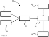
- FIG. 3 schematically illustrates a method 50 in accordance with the present invention.
- the method 50 starts in step 52 with application of an acoustic input signal to the sample.
- This may for example be performed using the transducer 18 illustrated in FIG. 1 or the modulated laser beam 42 provided by laser unit 40 of FIG. 2 .
- the transducer 18 of FIG. 1 may be used to provide a first acoustic signal and the pulsed laser source 40 of FIG. 2 , may be used to create additional acoustic vibrations, forming the second acoustic input signal in the probe tip 9.
- a probe tip 9 may also be provided with an additional actuator unit that acts as a transducer, such as element 18 in FIG. 1 .
- a probe 2 may be electrostatically actuated by means of applying any of a variety of existing methods. For example, this may be achieved by applying a variable voltage signal to the probe tip 9, while flexibly attaching the probe tip to the cantilever by means of leaf springs.
- an output signal is detected using the detection means of the scanning probe microscopy system.
- detection means include a laser beam 10 or 42 that impinges on the cantilever and is received by an optical detector, as is illustrated in FIGs. 1 or 2 above.
- the output signal 56 is provided to an analysis system.
- a reference signal 27 is created at the differential frequency f diff which is the difference between the frequency of the first acoustic input signal provided in step 52 and the further acoustic input signal provided in step 54.
- the reference signal 27 is also provided to the analysis system 30.
- step 58 the output signal 26 is analyzed by comparing it with the reference signal 27 received, and from this the amplitude and phase characteristics of the output signal 37 are determined.
- the amplitude and phase of the output signal are location dependent, and depend on the scanning position of the probe relative to the sample.
- the step of scanning the probe tip 9 relative to the sample 5 is not illustrated in the method 50 of FIG. 3 , but will usually be present to map the amplitude and phase data in a location dependent manner for visualization of the sub-surface structures 35. However, where desired the method of the present invention may also be used to obtain a single value at one location on the surface of the sample or to perform a line scan across one or more lines. It will be appreciated that the step of scanning the probe tip 9 relative to the sample 5 may be performed by any one of moving the probe tip 9 or moving the sample 5, or moving both the probe tip 9 and the sample 5. The invention is not limited to any particular implementation in this respect.
- step 62 After analyzing the output signal in step 58, the resulting amplitude and phase characteristics 37, together with the location data, are provided in step 62 as the outcome of the method of the present invention.
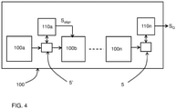
- FIG. 4 schematically shows a lithographic system 100 for manufacturing of a multilayer semiconductor device 5.
- the lithographic system 100 comprises an atomic force microscopy device 110a according to the second aspect of the invention.
- the lithographic system is arranged to manufacture the semiconductor device in mutually subsequent manufacturing stages 100a, 100b, ..100n.
- the mutually subsequent manufacturing stages 100a, 100b, ..100n at least comprise a first manufacturing stage 100a and a second manufacturing stage 100b.
- the atomic force microscopy device 110a is arranged to inspect a semi-finished product 5' obtained in the first manufacturing stage 100a and to provide an analysis signal S align indicative for a position of sub-surface features in the semi-finished product 5'.
- the lithographic system 100 is arranged to use the analysis signal S align for alignment of the semi-finished product 5' in the second manufacturing stage 100b.
- the lithographic system 100 comprises a further atomic force microscopy device 110n that analyzes a quality of the multilayer semiconductor device 5 and provides an output signal S Q indicative for said quality.
- the output signal S Q may be provided as a binary signal that indicates whether or not the quality of the semiconductor device meets predetermined requirements. Alternatively, or in addition the output signal SQ may provide diagnostic information enabling an operator of the lithographic system to improve its operation.
Landscapes
- Physics & Mathematics (AREA)
- Health & Medical Sciences (AREA)
- General Health & Medical Sciences (AREA)
- General Physics & Mathematics (AREA)
- Pathology (AREA)
- Immunology (AREA)
- Biochemistry (AREA)
- Life Sciences & Earth Sciences (AREA)
- Chemical & Material Sciences (AREA)
- Analytical Chemistry (AREA)
- Radiology & Medical Imaging (AREA)
- Nuclear Medicine, Radiotherapy & Molecular Imaging (AREA)
- Acoustics & Sound (AREA)
- Engineering & Computer Science (AREA)
- Power Engineering (AREA)
- Length Measuring Devices With Unspecified Measuring Means (AREA)
- Crystals, And After-Treatments Of Crystals (AREA)
- Analysing Materials By The Use Of Radiation (AREA)
Claims (11)
- Heterodynverfahren (50) zum Durchführen einer suboberflächlichen Detektion von Nanostrukturen in einer Probe (5) unter Verwendung eines Rasterkraftmikroskopiesystems, und wobei das Rasterkraftmikroskopiesystem wenigstens einen Abtastkopf (3) umfasst, wobei der Abtastkopf eine Sonde (2) einschließt, wobei die Sonde einen Ausleger (8) und eine auf dem Ausleger angeordnete Sondenspitze (9) umfasst, wobei das Verfahren umfasst:Bewegen der Sondenspitze (9) und der Probe (5) relativ zueinander in einer oder mehreren Richtungen parallel zur Oberfläche zum Abtasten der Oberfläche mit der Sondenspitze; undÜberwachen der Bewegung der Sondenspitze relativ zum Abtastkopf mit einem Spitzenpositionsdetektor während des Abtastens, um ein Ausgangssignal (26) zu erhalten (56);wobei das Verfahren ferner umfasst:während des Abtastens, Induzieren von akustischen Vibrationen in der Sondenspitze durch Anlegen (52) wenigstens eines ersten akustischen Eingangssignals, das eine Signalkomponente bei einer ersten Frequenz umfasst, an die Sonde, und Anlegen (54) zusätzlich zu dem wenigstens einen ersten akustischen Eingangssignal eines zweiten akustischen Eingangssignals, das eine zweite Signalkomponente bei einer zweiten Frequenz umfasst, wobei die erste und die zweite Frequenz sich gegenseitig unterscheidende Frequenzen sind;Analysieren (58) des Ausgangssignals (26) wenigstens zum Abbilden von suboberflächlichen Nanostrukturen unter der Oberfläche der Probe (5),dadurch gekennzeichnet, dass sowohl das erste als auch das zweite akustische Eingangssignal an die Sonde (2) angelegt werden, dass die erste und die zweite Frequenz Frequenzen über 1 Gigahertz sind, und dass eine Differenz zwischen der ersten und der zweiten Frequenz unter 1 Gigahertz liegt, wodurch ein gemischtes akustisches Signal erhalten wird, das eine dritte Signalkomponente mit einer Frequenz gleich der Differenz umfasst.
- Heterodynverfahren (50) nach Anspruch 1, wobei der Schritt des Induzierens der akustischen Vibrationen in der Sondenspitze unter Verwendung eines auf die Sondenspitze einfallenden optischen Anregungsstrahls (42) durchgeführt wird, wobei der optische Anregungsstrahl eine zeitlich variierende optische Leistung aufweist, um eine photothermische Anregung der Sondenspitze zum Induzieren der akustischen Vibrationen zu ermöglichen.
- Heterodynverfahren (50) nach einem der vorhergehenden Ansprüche, wobei der Schritt (56) des Abtastens des akustischen Ausgangssignals durch Erzeugen eines auf die Sondenspitze (9) einfallenden optischen Abtaststrahls (10), und Abtasten eines reflektierten Strahls (11) des optischen Abtaststrahls unter Verwendung eines optischen Sensors (20) durchgeführt wird.
- Heterodynverfahren (50) nach Anspruch 2 und 3, wobei der optische Abtaststrahl (42) so erzeugt wird, dass er eine zeitlich variierende optische Leistung umfasst, und wobei der optische Abtaststrahl auch den optischen Anregungsstrahl zum Induzieren der akustischen Vibrationen in der Sondenspitze (9) bildet.
- Heterodynverfahren (50) nach Anspruch 1, wobei der Schritt des Induzierens (52, 54) der akustischen Vibrationen in der Sondenspitze (9) mittels wenigstens einem einer Gruppe durchgeführt wird, die umfasst: einen akustischen Wandler (18), der mit dem Ausleger (8) oder der Sondenspitze (9) verbunden ist, einen piezoelektrischen Wandler, der mit dem Ausleger zusammenwirkt, einen elektrostatischen Aktuator, der mit dem Ausleger zusammenwirkt, einen elektrostatischen Aktuator, der mit der Sondenspitze zusammenwirkt, wobei die Sondenspitze flexibel an dem Ausleger angebracht ist, oder eine photothermische Anregung des Auslegers und/oder der Sondenspitze.
- Heterodynverfahren (50) nach einem der Ansprüche 2 bis 5, wobei der Schritt des Abtastens des akustischen Ausgangssignals das Bereitstellen eines Sensorsignals unter Verwendung eines Sensors umfasst, wobei das Verfahren ferner einen Schritt des Analysierens des ersten akustischen Eingangssignals mit dem zweiten akustischen Eingangssignal zum Bestimmen einer Differenz zwischen der ersten Frequenz und der zweiten Frequenz, des Erzeugens (60) eines Referenzsignals einschließlich einer Referenzsignalkomponente mit einer Frequenz gleich der Differenzfrequenz und des Analysierens (58) des Sensorsignals durch Vergleichen des Sensorsignals mit dem Referenzsignal umfasst.
- Heterodynverfahren (50) nach einem der vorhergehenden Ansprüche, wobei die Probe (5) ein Halbleiterbauelement ist, das einen Stapel von Bauelementschichten mit wenigstens einer ersten Schicht und einer zweiten Schicht umfasst.
- Heterodynverfahren (50) nach einem der Ansprüche 1 bis 6, wobei die Probe (5) ein halbfertiges mehrschichtiges Halbleiterbauelement ist, das eine strukturierte Bauelementschicht und eine Resistschicht umfasst, die eine oder mehrere Schichten einschließlich der strukturierten Bauelementschicht bedeckt.
- Heterodyn-Rasterkraftmikroskopievorrichtung (110a, 110n), wobei die Vorrichtung einen Abtastkopf (3) umfasst, wobei der Abtastkopf eine Sonde (2) einschließt, wobei die Sonde einen Ausleger (8) und eine Sondenspitze (9) umfasst, die auf dem Ausleger angeordnet ist, wobei die Vorrichtung ferner umfasst:einen Aktuator, der mit wenigstens einem Abtastkopf (3) und/oder einem Probenhalter zum Bewegen der Sondenspitze (9) und einer Probe (5) relativ zueinander in einer oder mehreren Richtungen parallel zu einer Oberfläche der Probe zum Abtasten der Oberfläche mit der Sondenspitze zusammenwirkt;einen Spitzenpositionsdetektor (20) zum Messen der Bewegung der Sondenspitze relativ zum Abtastkopf während des Abtastens, wobei der Detektor zum Bereitstellen eines Ausgangssignals (26) angeordnet ist, das die Bewegung angibt; undein Analysesystem (30) zum Empfangen und Analysieren des Ausgangssignals des Spitzenpositionsdetektors;wobei die Rasterkraftmikroskopievorrichtung ferner umfasst:einen Aktuator (18, 40) zum Induzieren akustischer Vibrationen in der Sondenspitze durch Anlegen wenigstens eines ersten akustischen Eingangssignals, das eine Signalkomponente mit einer ersten Frequenz (f1) umfasst, an die Sonde;Einrichtung zum Anlegen eines zweiten akustischen Eingangssignals, die eine zweite Signalkomponente mit einer zweiten Frequenz (f2) umfasst, wobei die erste und die zweite Frequenz sich gegenseitig unterscheidende Frequenzen sind;wobei das Analysesystem (30) zum Analysieren des Ausgangssignals (26) zum Abbilden wenigstens suboberflächlicher Nanostrukturen unter der Oberfläche der Probe angeordnet ist,dadurch gekennzeichnet, dass die Einrichtung zum Anlegen eines zweiten Eingangssignals ein Aktuator (18, 40) zum Induzieren akustischer Vibrationen in der Sondenspitze (9) durch Anlegen des zweiten akustischen Eingangssignals an die Sonde ist, dass die erste und die zweite Frequenz über 1 Gigahertz liegen und dass eine Differenz zwischen der ersten und der zweiten Frequenz unter 1 Gigahertz liegt, wodurch ein gemischtes akustisches Signal erhalten wird, das eine dritte Signalkomponente mit einer Frequenz gleich der Differenz umfasst.
- Heterodyn-Rasterkraftmikroskopievorrichtung nach Anspruch 9, wobei die Sondenspitze (9) konisch oder pyramidenförmig ist.
- Lithographisches System (100) zur Herstellung eines mehrschichtigen Halbleiterbauelements (5), wobei das System eine Heterodyn-Rasterkraftmikroskopievorrichtung (110a, 110n) nach Anspruch 9 oder 10 umfasst.
Applications Claiming Priority (2)
| Application Number | Priority Date | Filing Date | Title |
|---|---|---|---|
| EP17151417.7A EP3349017A1 (de) | 2017-01-13 | 2017-01-13 | Atomkraftmikroskopievorrichtung, -verfahren und lithographiesystem |
| PCT/NL2018/050027 WO2018132011A1 (en) | 2017-01-13 | 2018-01-15 | Heterodyne atomic force microscopy device, method and lithographic system |
Publications (2)
| Publication Number | Publication Date |
|---|---|
| EP3568704A1 EP3568704A1 (de) | 2019-11-20 |
| EP3568704B1 true EP3568704B1 (de) | 2022-03-02 |
Family
ID=57796252
Family Applications (2)
| Application Number | Title | Priority Date | Filing Date |
|---|---|---|---|
| EP17151417.7A Withdrawn EP3349017A1 (de) | 2017-01-13 | 2017-01-13 | Atomkraftmikroskopievorrichtung, -verfahren und lithographiesystem |
| EP18702353.6A Active EP3568704B1 (de) | 2017-01-13 | 2018-01-15 | Heterodyne rasterkraftmikroskopievorrichtung, -verfahren und lithographiesystem |
Family Applications Before (1)
| Application Number | Title | Priority Date | Filing Date |
|---|---|---|---|
| EP17151417.7A Withdrawn EP3349017A1 (de) | 2017-01-13 | 2017-01-13 | Atomkraftmikroskopievorrichtung, -verfahren und lithographiesystem |
Country Status (5)
| Country | Link |
|---|---|
| US (1) | US10942200B2 (de) |
| EP (2) | EP3349017A1 (de) |
| KR (1) | KR102484671B1 (de) |
| TW (1) | TWI766932B (de) |
| WO (1) | WO2018132011A1 (de) |
Families Citing this family (7)
| Publication number | Priority date | Publication date | Assignee | Title |
|---|---|---|---|---|
| EP3232192A1 (de) * | 2016-04-14 | 2017-10-18 | Nederlandse Organisatie voor toegepast- natuurwetenschappelijk onderzoek TNO | Verfahren zur heterodynen rastersondenmikroskopie, rastersondenmikroskopiesystem und sonde dafür |
| EP3742178A1 (de) * | 2019-05-21 | 2020-11-25 | Nederlandse Organisatie voor toegepast- natuurwetenschappelijk Onderzoek TNO | Heterodynes rastersondenmikroskopieverfahren und rastersondenmikroskopiesystem |
| EP3779600A1 (de) * | 2019-08-14 | 2021-02-17 | ASML Netherlands B.V. | Verfahren und metrologiewerkzeug zur bestimmung von informationen über eine zielstruktur und freitragende sonde |
| WO2021028174A1 (en) * | 2019-08-14 | 2021-02-18 | Asml Netherlands B.V. | Method and metrology tool for determining information about a target structure, and cantilever probe |
| NL2024739B1 (en) | 2020-01-23 | 2021-09-09 | Univ Delft Tech | Ultrasonic subsurface imaging microscopy device and method |
| US11668644B2 (en) * | 2021-03-30 | 2023-06-06 | Onto Innovation Inc. | Opto-acoustic measurement of a transparent film stack |
| CN113109595B (zh) * | 2021-04-09 | 2022-12-02 | 南方科技大学 | 一种解析静电与力电耦合响应的原子力显微方法及系统 |
Family Cites Families (10)
| Publication number | Priority date | Publication date | Assignee | Title |
|---|---|---|---|---|
| US5319977A (en) * | 1991-06-20 | 1994-06-14 | The Board Of Trustees Of The Leland Stanford Junior University | Near field acoustic ultrasonic microscope system and method |
| US8438927B2 (en) * | 2003-08-12 | 2013-05-14 | Northwestern University | Scanning near field thermoelastic acoustic holography (SNFTAH) |
| EP2150973B1 (de) * | 2007-05-10 | 2020-05-06 | Bruker Nano, Inc. | Zerstörungfreie unteroberflächen-ultraschallmikroskopie auf waferniveau unter verwendung von nahfeld-afm-detektion |
| US7845215B2 (en) * | 2007-05-31 | 2010-12-07 | The United States Of America As Represented By The Administrator Of The National Aeronautics And Space Administration | Resonant difference-frequency atomic force ultrasonic microscope |
| JP5277378B2 (ja) * | 2008-10-27 | 2013-08-28 | 国立大学法人金沢大学 | 走査型プローブ顕微鏡 |
| US20110231966A1 (en) * | 2010-03-17 | 2011-09-22 | Ali Passian | Scanning probe microscopy with spectroscopic molecular recognition |
| US9134341B2 (en) * | 2011-01-05 | 2015-09-15 | Craig Prater | Multiple modulation heterodyne infrared spectroscopy |
| CN103429526B (zh) * | 2011-01-31 | 2016-05-11 | 英菲尼特斯马有限公司 | 自适应模式扫描探针显微镜 |
| JP5765146B2 (ja) * | 2011-09-01 | 2015-08-19 | 株式会社島津製作所 | 原子間力顕微鏡におけるカンチレバー励振方法及び原子間力顕微鏡 |
| EP3232204A1 (de) * | 2016-04-14 | 2017-10-18 | Nederlandse Organisatie voor toegepast- natuurwetenschappelijk onderzoek TNO | Verfahren zur abstimmung von parametereinstellungen zum ausführen von akustischer rastersondenmikroskopie zur abbildung von unteroberflächenformationen, rastersondenmikroskopiesystem und computerprogrammprodukt |
-
2017
- 2017-01-13 EP EP17151417.7A patent/EP3349017A1/de not_active Withdrawn
-
2018
- 2018-01-15 WO PCT/NL2018/050027 patent/WO2018132011A1/en not_active Ceased
- 2018-01-15 EP EP18702353.6A patent/EP3568704B1/de active Active
- 2018-01-15 KR KR1020197022726A patent/KR102484671B1/ko active Active
- 2018-01-15 TW TW107101422A patent/TWI766932B/zh active
- 2018-01-15 US US16/477,633 patent/US10942200B2/en active Active
Also Published As
| Publication number | Publication date |
|---|---|
| KR102484671B1 (ko) | 2023-01-04 |
| KR20190107051A (ko) | 2019-09-18 |
| TWI766932B (zh) | 2022-06-11 |
| EP3568704A1 (de) | 2019-11-20 |
| EP3349017A1 (de) | 2018-07-18 |
| US10942200B2 (en) | 2021-03-09 |
| US20200124635A1 (en) | 2020-04-23 |
| WO2018132011A1 (en) | 2018-07-19 |
| TW201840976A (zh) | 2018-11-16 |
Similar Documents
| Publication | Publication Date | Title |
|---|---|---|
| US10942200B2 (en) | Heterodyne atomic force microscopy device, method and lithographic system | |
| US7584653B2 (en) | System for wide frequency dynamic nanomechanical analysis | |
| EP3568703B1 (de) | Atomkraftmikroskopievorrichtung, -verfahren und lithographiesystem | |
| US11940416B2 (en) | Heterodyne scanning probe microscopy method and system | |
| US11268935B2 (en) | Method of and atomic force microscopy system for performing subsurface imaging | |
| US20200124571A1 (en) | Method of and system for performing subsurface imaging using vibration sensing | |
| Kwoka et al. | Soft piezoresistive cantilevers for adhesion force measurements | |
| US11327092B2 (en) | Subsurface atomic force microscopy with guided ultrasound waves | |
| US12345737B2 (en) | Method, system and computer program for performing acoustic scanning probe microscopy | |
| EP3290929A1 (de) | Verfahren zur messung des durch einen elektronenstrahl verursachten schadens eines substrats | |
| Parlak et al. | Quantitative subsurface imaging by acoustic AFM techniques | |
| Sierakowski et al. | Dynamic method of calibration and examination piezoresistive cantilevers | |
| Evans et al. | Characterizing absolute piezoelectric microelectromechanical system displacement using an atomic force microscope | |
| Parlak | Quantitative imaging of subsurface structures and mechanical properties at nanoscale using atomic force microscope |
Legal Events
| Date | Code | Title | Description |
|---|---|---|---|
| STAA | Information on the status of an ep patent application or granted ep patent |
Free format text: STATUS: UNKNOWN |
|
| STAA | Information on the status of an ep patent application or granted ep patent |
Free format text: STATUS: THE INTERNATIONAL PUBLICATION HAS BEEN MADE |
|
| PUAI | Public reference made under article 153(3) epc to a published international application that has entered the european phase |
Free format text: ORIGINAL CODE: 0009012 |
|
| STAA | Information on the status of an ep patent application or granted ep patent |
Free format text: STATUS: REQUEST FOR EXAMINATION WAS MADE |
|
| 17P | Request for examination filed |
Effective date: 20190731 |
|
| AK | Designated contracting states |
Kind code of ref document: A1 Designated state(s): AL AT BE BG CH CY CZ DE DK EE ES FI FR GB GR HR HU IE IS IT LI LT LU LV MC MK MT NL NO PL PT RO RS SE SI SK SM TR |
|
| AX | Request for extension of the european patent |
Extension state: BA ME |
|
| DAV | Request for validation of the european patent (deleted) | ||
| DAX | Request for extension of the european patent (deleted) | ||
| GRAP | Despatch of communication of intention to grant a patent |
Free format text: ORIGINAL CODE: EPIDOSNIGR1 |
|
| STAA | Information on the status of an ep patent application or granted ep patent |
Free format text: STATUS: GRANT OF PATENT IS INTENDED |
|
| INTG | Intention to grant announced |
Effective date: 20210816 |
|
| GRAS | Grant fee paid |
Free format text: ORIGINAL CODE: EPIDOSNIGR3 |
|
| GRAA | (expected) grant |
Free format text: ORIGINAL CODE: 0009210 |
|
| STAA | Information on the status of an ep patent application or granted ep patent |
Free format text: STATUS: THE PATENT HAS BEEN GRANTED |
|
| AK | Designated contracting states |
Kind code of ref document: B1 Designated state(s): AL AT BE BG CH CY CZ DE DK EE ES FI FR GB GR HR HU IE IS IT LI LT LU LV MC MK MT NL NO PL PT RO RS SE SI SK SM TR |
|
| REG | Reference to a national code |
Ref country code: GB Ref legal event code: FG4D |
|
| REG | Reference to a national code |
Ref country code: CH Ref legal event code: EP Ref country code: AT Ref legal event code: REF Ref document number: 1472683 Country of ref document: AT Kind code of ref document: T Effective date: 20220315 |
|
| REG | Reference to a national code |
Ref country code: DE Ref legal event code: R096 Ref document number: 602018031552 Country of ref document: DE |
|
| REG | Reference to a national code |
Ref country code: IE Ref legal event code: FG4D |
|
| REG | Reference to a national code |
Ref country code: NL Ref legal event code: FP |
|
| REG | Reference to a national code |
Ref country code: LT Ref legal event code: MG9D |
|
| PG25 | Lapsed in a contracting state [announced via postgrant information from national office to epo] |
Ref country code: SE Free format text: LAPSE BECAUSE OF FAILURE TO SUBMIT A TRANSLATION OF THE DESCRIPTION OR TO PAY THE FEE WITHIN THE PRESCRIBED TIME-LIMIT Effective date: 20220302 Ref country code: RS Free format text: LAPSE BECAUSE OF FAILURE TO SUBMIT A TRANSLATION OF THE DESCRIPTION OR TO PAY THE FEE WITHIN THE PRESCRIBED TIME-LIMIT Effective date: 20220302 Ref country code: NO Free format text: LAPSE BECAUSE OF FAILURE TO SUBMIT A TRANSLATION OF THE DESCRIPTION OR TO PAY THE FEE WITHIN THE PRESCRIBED TIME-LIMIT Effective date: 20220602 Ref country code: LT Free format text: LAPSE BECAUSE OF FAILURE TO SUBMIT A TRANSLATION OF THE DESCRIPTION OR TO PAY THE FEE WITHIN THE PRESCRIBED TIME-LIMIT Effective date: 20220302 Ref country code: HR Free format text: LAPSE BECAUSE OF FAILURE TO SUBMIT A TRANSLATION OF THE DESCRIPTION OR TO PAY THE FEE WITHIN THE PRESCRIBED TIME-LIMIT Effective date: 20220302 Ref country code: ES Free format text: LAPSE BECAUSE OF FAILURE TO SUBMIT A TRANSLATION OF THE DESCRIPTION OR TO PAY THE FEE WITHIN THE PRESCRIBED TIME-LIMIT Effective date: 20220302 Ref country code: BG Free format text: LAPSE BECAUSE OF FAILURE TO SUBMIT A TRANSLATION OF THE DESCRIPTION OR TO PAY THE FEE WITHIN THE PRESCRIBED TIME-LIMIT Effective date: 20220602 |
|
| REG | Reference to a national code |
Ref country code: AT Ref legal event code: MK05 Ref document number: 1472683 Country of ref document: AT Kind code of ref document: T Effective date: 20220302 |
|
| PG25 | Lapsed in a contracting state [announced via postgrant information from national office to epo] |
Ref country code: PL Free format text: LAPSE BECAUSE OF FAILURE TO SUBMIT A TRANSLATION OF THE DESCRIPTION OR TO PAY THE FEE WITHIN THE PRESCRIBED TIME-LIMIT Effective date: 20220302 Ref country code: LV Free format text: LAPSE BECAUSE OF FAILURE TO SUBMIT A TRANSLATION OF THE DESCRIPTION OR TO PAY THE FEE WITHIN THE PRESCRIBED TIME-LIMIT Effective date: 20220302 Ref country code: GR Free format text: LAPSE BECAUSE OF FAILURE TO SUBMIT A TRANSLATION OF THE DESCRIPTION OR TO PAY THE FEE WITHIN THE PRESCRIBED TIME-LIMIT Effective date: 20220603 Ref country code: FI Free format text: LAPSE BECAUSE OF FAILURE TO SUBMIT A TRANSLATION OF THE DESCRIPTION OR TO PAY THE FEE WITHIN THE PRESCRIBED TIME-LIMIT Effective date: 20220302 |
|
| PG25 | Lapsed in a contracting state [announced via postgrant information from national office to epo] |
Ref country code: SM Free format text: LAPSE BECAUSE OF FAILURE TO SUBMIT A TRANSLATION OF THE DESCRIPTION OR TO PAY THE FEE WITHIN THE PRESCRIBED TIME-LIMIT Effective date: 20220302 Ref country code: SK Free format text: LAPSE BECAUSE OF FAILURE TO SUBMIT A TRANSLATION OF THE DESCRIPTION OR TO PAY THE FEE WITHIN THE PRESCRIBED TIME-LIMIT Effective date: 20220302 Ref country code: RO Free format text: LAPSE BECAUSE OF FAILURE TO SUBMIT A TRANSLATION OF THE DESCRIPTION OR TO PAY THE FEE WITHIN THE PRESCRIBED TIME-LIMIT Effective date: 20220302 Ref country code: PT Free format text: LAPSE BECAUSE OF FAILURE TO SUBMIT A TRANSLATION OF THE DESCRIPTION OR TO PAY THE FEE WITHIN THE PRESCRIBED TIME-LIMIT Effective date: 20220704 Ref country code: EE Free format text: LAPSE BECAUSE OF FAILURE TO SUBMIT A TRANSLATION OF THE DESCRIPTION OR TO PAY THE FEE WITHIN THE PRESCRIBED TIME-LIMIT Effective date: 20220302 Ref country code: CZ Free format text: LAPSE BECAUSE OF FAILURE TO SUBMIT A TRANSLATION OF THE DESCRIPTION OR TO PAY THE FEE WITHIN THE PRESCRIBED TIME-LIMIT Effective date: 20220302 Ref country code: AT Free format text: LAPSE BECAUSE OF FAILURE TO SUBMIT A TRANSLATION OF THE DESCRIPTION OR TO PAY THE FEE WITHIN THE PRESCRIBED TIME-LIMIT Effective date: 20220302 |
|
| PG25 | Lapsed in a contracting state [announced via postgrant information from national office to epo] |
Ref country code: IS Free format text: LAPSE BECAUSE OF FAILURE TO SUBMIT A TRANSLATION OF THE DESCRIPTION OR TO PAY THE FEE WITHIN THE PRESCRIBED TIME-LIMIT Effective date: 20220702 Ref country code: AL Free format text: LAPSE BECAUSE OF FAILURE TO SUBMIT A TRANSLATION OF THE DESCRIPTION OR TO PAY THE FEE WITHIN THE PRESCRIBED TIME-LIMIT Effective date: 20220302 |
|
| REG | Reference to a national code |
Ref country code: DE Ref legal event code: R097 Ref document number: 602018031552 Country of ref document: DE |
|
| PLBE | No opposition filed within time limit |
Free format text: ORIGINAL CODE: 0009261 |
|
| STAA | Information on the status of an ep patent application or granted ep patent |
Free format text: STATUS: NO OPPOSITION FILED WITHIN TIME LIMIT |
|
| PG25 | Lapsed in a contracting state [announced via postgrant information from national office to epo] |
Ref country code: DK Free format text: LAPSE BECAUSE OF FAILURE TO SUBMIT A TRANSLATION OF THE DESCRIPTION OR TO PAY THE FEE WITHIN THE PRESCRIBED TIME-LIMIT Effective date: 20220302 |
|
| 26N | No opposition filed |
Effective date: 20221205 |
|
| PG25 | Lapsed in a contracting state [announced via postgrant information from national office to epo] |
Ref country code: SI Free format text: LAPSE BECAUSE OF FAILURE TO SUBMIT A TRANSLATION OF THE DESCRIPTION OR TO PAY THE FEE WITHIN THE PRESCRIBED TIME-LIMIT Effective date: 20220302 |
|
| P01 | Opt-out of the competence of the unified patent court (upc) registered |
Effective date: 20230522 |
|
| PG25 | Lapsed in a contracting state [announced via postgrant information from national office to epo] |
Ref country code: IT Free format text: LAPSE BECAUSE OF FAILURE TO SUBMIT A TRANSLATION OF THE DESCRIPTION OR TO PAY THE FEE WITHIN THE PRESCRIBED TIME-LIMIT Effective date: 20220302 |
|
| REG | Reference to a national code |
Ref country code: CH Ref legal event code: PL |
|
| GBPC | Gb: european patent ceased through non-payment of renewal fee |
Effective date: 20230115 |
|
| PG25 | Lapsed in a contracting state [announced via postgrant information from national office to epo] |
Ref country code: LU Free format text: LAPSE BECAUSE OF NON-PAYMENT OF DUE FEES Effective date: 20230115 |
|
| REG | Reference to a national code |
Ref country code: BE Ref legal event code: MM Effective date: 20230131 |
|
| PG25 | Lapsed in a contracting state [announced via postgrant information from national office to epo] |
Ref country code: LI Free format text: LAPSE BECAUSE OF NON-PAYMENT OF DUE FEES Effective date: 20230131 Ref country code: GB Free format text: LAPSE BECAUSE OF NON-PAYMENT OF DUE FEES Effective date: 20230115 Ref country code: CH Free format text: LAPSE BECAUSE OF NON-PAYMENT OF DUE FEES Effective date: 20230131 |
|
| PG25 | Lapsed in a contracting state [announced via postgrant information from national office to epo] |
Ref country code: BE Free format text: LAPSE BECAUSE OF NON-PAYMENT OF DUE FEES Effective date: 20230131 |
|
| PG25 | Lapsed in a contracting state [announced via postgrant information from national office to epo] |
Ref country code: MC Free format text: LAPSE BECAUSE OF FAILURE TO SUBMIT A TRANSLATION OF THE DESCRIPTION OR TO PAY THE FEE WITHIN THE PRESCRIBED TIME-LIMIT Effective date: 20220302 |
|
| PG25 | Lapsed in a contracting state [announced via postgrant information from national office to epo] |
Ref country code: MC Free format text: LAPSE BECAUSE OF FAILURE TO SUBMIT A TRANSLATION OF THE DESCRIPTION OR TO PAY THE FEE WITHIN THE PRESCRIBED TIME-LIMIT Effective date: 20220302 |
|
| PG25 | Lapsed in a contracting state [announced via postgrant information from national office to epo] |
Ref country code: CY Free format text: LAPSE BECAUSE OF FAILURE TO SUBMIT A TRANSLATION OF THE DESCRIPTION OR TO PAY THE FEE WITHIN THE PRESCRIBED TIME-LIMIT; INVALID AB INITIO Effective date: 20180115 |
|
| PG25 | Lapsed in a contracting state [announced via postgrant information from national office to epo] |
Ref country code: HU Free format text: LAPSE BECAUSE OF FAILURE TO SUBMIT A TRANSLATION OF THE DESCRIPTION OR TO PAY THE FEE WITHIN THE PRESCRIBED TIME-LIMIT; INVALID AB INITIO Effective date: 20180115 |
|
| PG25 | Lapsed in a contracting state [announced via postgrant information from national office to epo] |
Ref country code: TR Free format text: LAPSE BECAUSE OF FAILURE TO SUBMIT A TRANSLATION OF THE DESCRIPTION OR TO PAY THE FEE WITHIN THE PRESCRIBED TIME-LIMIT Effective date: 20220302 |
|
| PGFP | Annual fee paid to national office [announced via postgrant information from national office to epo] |
Ref country code: NL Payment date: 20260121 Year of fee payment: 9 |
|
| PGFP | Annual fee paid to national office [announced via postgrant information from national office to epo] |
Ref country code: DE Payment date: 20260121 Year of fee payment: 9 Ref country code: IE Payment date: 20260122 Year of fee payment: 9 |
|
| PGFP | Annual fee paid to national office [announced via postgrant information from national office to epo] |
Ref country code: FR Payment date: 20260123 Year of fee payment: 9 |