EP3576270A1 - Onduleur à tension de commande de grille avec une tension élevé à température de la couche d'arrêt élevée - Google Patents
Onduleur à tension de commande de grille avec une tension élevé à température de la couche d'arrêt élevée Download PDFInfo
- Publication number
- EP3576270A1 EP3576270A1 EP18174871.6A EP18174871A EP3576270A1 EP 3576270 A1 EP3576270 A1 EP 3576270A1 EP 18174871 A EP18174871 A EP 18174871A EP 3576270 A1 EP3576270 A1 EP 3576270A1
- Authority
- EP
- European Patent Office
- Prior art keywords
- potential
- control device
- switching element
- switching
- converter
- Prior art date
- Legal status (The legal status is an assumption and is not a legal conclusion. Google has not performed a legal analysis and makes no representation as to the accuracy of the status listed.)
- Withdrawn
Links
- 230000000903 blocking effect Effects 0.000 claims abstract description 6
- 238000011017 operating method Methods 0.000 claims description 23
- 239000004065 semiconductor Substances 0.000 claims description 14
- 230000007704 transition Effects 0.000 claims description 5
- 230000007423 decrease Effects 0.000 abstract description 9
- 230000004888 barrier function Effects 0.000 abstract description 3
- 230000008859 change Effects 0.000 description 5
- 230000000694 effects Effects 0.000 description 5
- 230000008901 benefit Effects 0.000 description 3
- 230000009467 reduction Effects 0.000 description 3
- HBMJWWWQQXIZIP-UHFFFAOYSA-N silicon carbide Chemical compound [Si+]#[C-] HBMJWWWQQXIZIP-UHFFFAOYSA-N 0.000 description 3
- 229910010271 silicon carbide Inorganic materials 0.000 description 3
- 230000001133 acceleration Effects 0.000 description 2
- 230000032683 aging Effects 0.000 description 2
- 230000001419 dependent effect Effects 0.000 description 2
- 238000013461 design Methods 0.000 description 2
- 238000000034 method Methods 0.000 description 2
- 206010063493 Premature ageing Diseases 0.000 description 1
- 208000032038 Premature aging Diseases 0.000 description 1
- 238000013459 approach Methods 0.000 description 1
- 239000003990 capacitor Substances 0.000 description 1
- 239000002826 coolant Substances 0.000 description 1
- 238000010586 diagram Methods 0.000 description 1
- 230000005611 electricity Effects 0.000 description 1
- 238000012886 linear function Methods 0.000 description 1
- 238000012545 processing Methods 0.000 description 1
- 229910052710 silicon Inorganic materials 0.000 description 1
- 239000010703 silicon Substances 0.000 description 1
- 238000004804 winding Methods 0.000 description 1
Images




Classifications
-
- H—ELECTRICITY
- H02—GENERATION; CONVERSION OR DISTRIBUTION OF ELECTRIC POWER
- H02M—APPARATUS FOR CONVERSION BETWEEN AC AND AC, BETWEEN AC AND DC, OR BETWEEN DC AND DC, AND FOR USE WITH MAINS OR SIMILAR POWER SUPPLY SYSTEMS; CONVERSION OF DC OR AC INPUT POWER INTO SURGE OUTPUT POWER; CONTROL OR REGULATION THEREOF
- H02M1/00—Details of apparatus for conversion
- H02M1/32—Means for protecting converters other than automatic disconnection
-
- H—ELECTRICITY
- H02—GENERATION; CONVERSION OR DISTRIBUTION OF ELECTRIC POWER
- H02M—APPARATUS FOR CONVERSION BETWEEN AC AND AC, BETWEEN AC AND DC, OR BETWEEN DC AND DC, AND FOR USE WITH MAINS OR SIMILAR POWER SUPPLY SYSTEMS; CONVERSION OF DC OR AC INPUT POWER INTO SURGE OUTPUT POWER; CONTROL OR REGULATION THEREOF
- H02M1/00—Details of apparatus for conversion
- H02M1/08—Circuits specially adapted for the generation of control voltages for semiconductor devices incorporated in static converters
-
- H—ELECTRICITY
- H02—GENERATION; CONVERSION OR DISTRIBUTION OF ELECTRIC POWER
- H02M—APPARATUS FOR CONVERSION BETWEEN AC AND AC, BETWEEN AC AND DC, OR BETWEEN DC AND DC, AND FOR USE WITH MAINS OR SIMILAR POWER SUPPLY SYSTEMS; CONVERSION OF DC OR AC INPUT POWER INTO SURGE OUTPUT POWER; CONTROL OR REGULATION THEREOF
- H02M1/00—Details of apparatus for conversion
- H02M1/0048—Circuits or arrangements for reducing losses
-
- H—ELECTRICITY
- H02—GENERATION; CONVERSION OR DISTRIBUTION OF ELECTRIC POWER
- H02M—APPARATUS FOR CONVERSION BETWEEN AC AND AC, BETWEEN AC AND DC, OR BETWEEN DC AND DC, AND FOR USE WITH MAINS OR SIMILAR POWER SUPPLY SYSTEMS; CONVERSION OF DC OR AC INPUT POWER INTO SURGE OUTPUT POWER; CONTROL OR REGULATION THEREOF
- H02M1/00—Details of apparatus for conversion
- H02M1/32—Means for protecting converters other than automatic disconnection
- H02M1/327—Means for protecting converters other than automatic disconnection against abnormal temperatures
-
- H—ELECTRICITY
- H02—GENERATION; CONVERSION OR DISTRIBUTION OF ELECTRIC POWER
- H02M—APPARATUS FOR CONVERSION BETWEEN AC AND AC, BETWEEN AC AND DC, OR BETWEEN DC AND DC, AND FOR USE WITH MAINS OR SIMILAR POWER SUPPLY SYSTEMS; CONVERSION OF DC OR AC INPUT POWER INTO SURGE OUTPUT POWER; CONTROL OR REGULATION THEREOF
- H02M7/00—Conversion of AC power input into DC power output; Conversion of DC power input into AC power output
- H02M7/42—Conversion of DC power input into AC power output without possibility of reversal
- H02M7/44—Conversion of DC power input into AC power output without possibility of reversal by static converters
- H02M7/48—Conversion of DC power input into AC power output without possibility of reversal by static converters using discharge tubes with control electrode or semiconductor devices with control electrode
- H02M7/53—Conversion of DC power input into AC power output without possibility of reversal by static converters using discharge tubes with control electrode or semiconductor devices with control electrode using devices of a triode or transistor type requiring continuous application of a control signal
- H02M7/537—Conversion of DC power input into AC power output without possibility of reversal by static converters using discharge tubes with control electrode or semiconductor devices with control electrode using devices of a triode or transistor type requiring continuous application of a control signal using semiconductor devices only, e.g. single switched pulse inverters
- H02M7/5387—Conversion of DC power input into AC power output without possibility of reversal by static converters using discharge tubes with control electrode or semiconductor devices with control electrode using devices of a triode or transistor type requiring continuous application of a control signal using semiconductor devices only, e.g. single switched pulse inverters in a bridge configuration
-
- H—ELECTRICITY
- H03—ELECTRONIC CIRCUITRY
- H03K—PULSE TECHNIQUE
- H03K17/00—Electronic switching or gating, i.e. not by contact-making and –breaking
- H03K17/06—Modifications for ensuring a fully conducting state
-
- H—ELECTRICITY
- H03—ELECTRONIC CIRCUITRY
- H03K—PULSE TECHNIQUE
- H03K17/00—Electronic switching or gating, i.e. not by contact-making and –breaking
- H03K17/08—Modifications for protecting switching circuit against overcurrent or overvoltage
- H03K2017/0806—Modifications for protecting switching circuit against overcurrent or overvoltage against excessive temperature
-
- Y—GENERAL TAGGING OF NEW TECHNOLOGICAL DEVELOPMENTS; GENERAL TAGGING OF CROSS-SECTIONAL TECHNOLOGIES SPANNING OVER SEVERAL SECTIONS OF THE IPC; TECHNICAL SUBJECTS COVERED BY FORMER USPC CROSS-REFERENCE ART COLLECTIONS [XRACs] AND DIGESTS
- Y02—TECHNOLOGIES OR APPLICATIONS FOR MITIGATION OR ADAPTATION AGAINST CLIMATE CHANGE
- Y02B—CLIMATE CHANGE MITIGATION TECHNOLOGIES RELATED TO BUILDINGS, e.g. HOUSING, HOUSE APPLIANCES OR RELATED END-USER APPLICATIONS
- Y02B70/00—Technologies for an efficient end-user side electric power management and consumption
- Y02B70/10—Technologies improving the efficiency by using switched-mode power supplies [SMPS], i.e. efficient power electronics conversion e.g. power factor correction or reduction of losses in power supplies or efficient standby modes
Definitions
- the present invention is based on an operating method for a load-feeding converter.
- the control device takes clocked each receives a current setpoint and determines switching times for switching elements of the inverter, to which the control device blocks the switching elements alternately and turns on.
- the switching elements are designed as semiconductor components. The switching times are determined in such a way that the converter supplies a current corresponding to the current setpoint to the load.
- the control device assumes nominal or actual variables-usually actual values-and derives therefrom a junction temperature of the switching elements. As long as the junction temperature does not reach or exceed an upper limit temperature, the control device retains the determined switching times unchanged. Otherwise, it determines the switching times such that the current supplied to the load is smaller than the current setpoint.
- the control device blocks the switching elements at the determined switching times in each case or switches them through in each case. For blocking a respective switching element, the control device switches on a first potential to a control electrode of the respective switching element, for switching through a second potential.
- the present invention is further based on a control program for a control device of an inverter, the control program having machine code that can be executed by the control device, wherein the processing of the machine code by the control device causes the control device to operate the converter according to such an operating method.
- the present invention is further based on a control device for a converter, wherein the control device is programmed with such a control program, so that the control device operates the converter according to such an operating method.
- the present invention is further based on a converter, wherein the converter comprises semiconductor elements formed as switching elements, via which a load is fed, wherein the inverter comprises such a control device which operates the inverter according to such an operating method.
- the power loss occurring at the respective semiconductor element results from the product of the current conducted by the respective semiconductor element with the respective forward voltage.
- the current is a non-linear function (characteristic curve) of the forward voltage, the function itself being dependent on the control voltage of the semiconductor.
- the determined switching times are redetermined such that the current supplied to the load is smaller than the current setpoint.
- the proportion to which the switching elements are connected can be reduced.
- a lower current flows in the result, whereby the resulting power loss is reduced accordingly.
- Due to the reduced current continues to decrease - even if only slightly - the forward voltage, so that the resulting power loss even further is reduced. This reduces the junction temperature.
- the reduction of the current takes place only so far that the limit temperature is just kept.
- the actually desired operation of the load is abandoned, albeit to protect the converter.
- the load is operated at a lower power than actually desired. For example, a drive can deliver only a lesser moment than actually desired.
- the object of the present invention is to provide means by which in a variety of applications, the desired operation of the load can be maintained, although this is not possible if to lock a respective switching element of the inverter, a first potential and for switching through the respective Switching element, a second potential is turned on to a control electrode of the respective switching element.
- the control device thus initially operates in normal operation as is well known.
- the control device goes into the special mode, in which the control device for switching through the respective switching element at least temporarily turns on a third potential to the control electrode of the respective switching element, wherein the third potential is above the second potential. Only when the junction temperature does not drop despite a transition from normal operation to special operation, or after such a decrease in special operation again reaches or exceeds the upper limit temperature, the current is reduced.
- the present invention is based on the consideration that by increasing the potential for switching through the respective switching element, the forward voltage required for the same current decreases and thereby the power loss would also have to decrease or decrease accordingly.
- the load may be the traction drive of the road vehicle.
- full load is needed only during extreme acceleration or uphill driving.
- uphill driving As a rule - especially in urban traffic and overland traffic -
- only a small part of the rated load is needed, often well below 50%.
- Similar facts apply, for example, to electrically operated rail vehicles.
- operation under full load is normally only needed if there is a short-term acceleration, especially when driving uphill.
- the load only works with part of its nominal load, often also far below 50%.
- the third potential it is only necessary to select the third potential in such a way that, on the one hand, the third potential has a sufficient distance from the second potential, so that the forward voltage is significantly lower for the same current, but on the other hand the third potential is still so low that the Switching element is not directly damaged.
- An appropriate determination of the third potential is readily possible.
- control device in the special mode for switching through the respective switching element only the third potential to the control electrode of the respective switching element turns on. By doing so, a maximum thermal relief of the barrier layer of the switching elements is achieved.
- the control device in the special mode it is possible for the control device in the special mode to switch on the respective switching element first to the respective switching time the second potential and only then the third potential to the control electrode of the respective switching element.
- the actually flowing current can be limited to lower values than if the third potential were immediately connected to the control electrode of the respective switching element.
- the second potential should only be used for a short time.
- the proportion to which the controller turns on the third potential to the control electrode of the respective switching element greater than the proportion to which the controller turns on the second potential to the control electrode of the respective switching element.
- the proportion based on the period between the beginning and the end of the switching of the respective switching element, at least 80%, for example at least 90%.
- the third potential should differ to a sufficient extent from the second potential. In practice, this is usually achieved by making the third potential, based on the first potential, at least 10% larger than the second potential. So it should be the relationship P 3 - P 1 P 2 - P 1 > 1 . 1 be valid.
- P1, P2 and P3 are the first, the second and the third potential.
- the third potential is at least 20% greater than the second potential, in particular at least 30%.
- the third potential must not be so high that damage to the switching element occurs very quickly. In practice, this is usually achieved by making the third potential, based on the first potential, no more than 100% larger than the second potential. So it should be the relationship P 3 - P 1 P 2 - P 1 ⁇ 2 . 0 be valid.
- the third potential, based on the first potential is at most 80% greater than the second potential, in particular by a maximum of 50%.
- the third potential is preferably 3V to 10V larger than the second potential. So it should preferably be the relationship 3 V ⁇ P 3 - P 2 ⁇ 10 V be valid. In particular, the third potential may be 4V to 8V above the second potential.
- the second potential may be at normal levels. In practice, in many cases, the second potential will be 8V to 30V larger than the first potential. So it should preferably be the relationship 8th V ⁇ P 2 - P 1 ⁇ 30 V be valid. Usually the second potential will be 12V to 20V above the first potential, for example at 15V, 17V or 18V.
- control program having the features of claim 9.
- the execution of the machine code by the control device causes the control device to operate the converter in accordance with an operating method according to the invention.
- control device for a converter with the features of claim 10.
- the control device is programmed with a control program according to the invention, so that the control device operates the converter in accordance with an operating method according to the invention.
- the converter has a control device according to the invention, which operates the converter in accordance with an operating method according to the invention.
- an inverter 1 is fed from a supply network 2.
- the inverter 1 to be connected via a rectifier 3 to the supply network 2.
- an intermediate circuit capacitor 4 is generally present between the converter 1 and the rectifier 3.
- the inverter 1 may be designed as a direct converter, which is connected directly to the supply network 2.
- the inverter 1 can be powered instead of the supply network 2 from a battery.
- a load 5 is fed, that is supplied with electrical energy.
- the connection of the voltage U present on the input side of the converter 1 to the load 5 does not lead to power surges, but that current increases and current drops are smoothed.
- Chokes 6 may be arranged between the inverter 1 and the load 5 for this purpose. But there are also other configurations possible.
- the load 5 is an electric machine, the necessary effect can also be effected by the windings of the electric machine as such.
- the inverter 1 has according to FIG. 2 Switching elements 7 on.
- the switching elements 7 are formed as semiconductor components.
- the converter 1 has a control device 8.
- the control device 8 is programmed with a control program 9.
- the control program 9 comprises machine code 10, which can be processed by the control device 8.
- the execution of the machine code 10 by the controller 8 causes the controller 8 to operate the inverter 1 according to an operating method which will be explained later.
- controller 8 controls, as in FIG. 1 indicated by dashed lines, and the rectifier 1.
- this is in the context of the present invention is of minor importance.
- the operating method according to the invention is explained in connection with a single one of the switching elements 7. However, it is executed by the control device 8 for all switching elements 7.
- the control device 8 operates the converter 1 alternatively in a normal mode or in a special mode.
- FIG. 3 shows in the left column is the normal mode, in the right column the special mode.
- the control device 8 accepts a current setpoint I * in a step S1.
- the control device 8 determines the respective switching times tij for the switching elements 7.
- the control device 8 thus determines - see FIG. 4 those times tij to which the respective switching element 7 is to be switched through or to be blocked.
- the respective switching element 7 conducts electricity, not in the locked state.
- the determination of step S2 is carried out by the control device 8 such that a current I (see FIG. 5 ), which flows through the respective switching element 7 in the through-connected state, is equal to the respective current setpoint I *.
- the switching elements 7 are often controlled pulse width modulated. Pulse width modulation means that the switching times tij, are determined such that in a fixed period - the reciprocal of the pulse repetition frequency - the corresponding switching element 7 is turned on during a first part of this period and locked during a second part of this period, the first and the second part together give the said period. If the first part and the second part are the same size, it is called a 50% duty cycle. If the first part is smaller than the second part, the duty cycle is less than 50%, in the opposite case more than 50%. The size of the duty cycle can be used to set how large the current I is.
- the control device 8 thus determined as a result of the current setpoint I * the required duty cycle and then determines based on the duty cycle, the switching times tij.
- the working clock can match the reciprocal of the pulse repetition frequency.
- the working clock may be a multiple - in particular an integer multiple of the reciprocal of the pulse repetition frequency.
- the control device 8 continues to receive setpoint or actual variables in a step S3.
- the control device 8 - see FIG. 2 - Accept the load 5 supplied phase currents Ik and assign the respective switching element 7.
- the control device 8 derives a junction temperature T of the respective switching element 7 from the quantities taken in step S3.
- the control device 8 in step S4 based on a potential P2, the normal operation for switching through the corresponding switching element 7 to a control electrode 11 of the switching element 7 - see FIG.
- the junction temperature T can be derived.
- the control device 8 it is possible for the control device 8 to receive a quantity related to a predetermined time unit (for example 1 s) and a temperature of a cooling medium with which the switching elements 7 are cooled, and from this determines the junction temperature T.
- a predetermined time unit for example 1 s
- the control device 8 checks whether the determined junction temperature T remains below an upper limit temperature TGO.
- the upper limit temperature TGO is determined as a function of the switching elements 7 used as needed. For example, it may be at 150 ° C.
- step S5 the controller 8 maintains the normal operation. In particular, the controller 8 proceeds to step S6 in this case.
- step S6 the control device 8 controls the corresponding switching element 7 such that the corresponding switching element 7 at the determined switching times tij each locks or connects. For each switching time tij, the switching element 7 thus changes its driving state. From step S6, the controller 8 returns to step S1.
- the control device 8 switches as shown in the 4 to 7 a first potential P1 to the control electrode 11, for turning on a second potential P2.
- the second potential P2 is generally larger by 8 V to 30 V than the first potential P1, in particular by 10 V to 20 V.
- the first potential P1 is at 0 V
- the second potential P2 at 15 V.
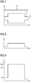
- FIG. 4 shows with respect to one of the switching elements 7 two immediately successive switching times tij, wherein the corresponding switching element 7 is switched through to the earlier switching time tij and locked at the later switching time.
- FIG. 6 shows the associated time course of the pending at the control electrode 11 of the corresponding switching element 7 potential P as a function of time t.
- FIG. 7 shows the associated switching positions of switches 12, 12 'and 12 ", by means of which the potentials P1, P2 and another potential P3 are turned on to the corresponding control electrode 11.
- resistors 13 are of minor importance. They merely serve to cushion sudden transitions when the driving state is changed, that is to say when the potential P supplied to the respective control electrode 11 is changed. In the stable state, the respective potential P1, P2 or P3 is always applied to the respective control electrode 11.
- the control device 8 switches to the special mode. Specifically, the controller 8 proceeds to a step S7 or a step S8. Steps S7 and S8 are in FIG. 3 dashed lines, because of the steps S7 and S8 only one is present, so either the step S7 or step S8.
- step S7 the control device 8 - analogous to step S6 - controls the corresponding switching element 7 such that the corresponding switching element 7 blocks or switches through to the determined switching times tij. For each switching time tij, the switching element 7 thus changes its driving state.
- the control device 8 switches - analogously to step S6 - as shown in the FIGS. 8 to 10 the first potential P1 to the control electrode 1, for switching through but instead of the second potential P2, the third potential P3.
- FIG. 8 shows with respect to one of the switching elements 7 two immediately successive switching times tij, wherein the corresponding switching element 7 is switched through to the earlier switching time tij and locked at the later switching time.
- FIG. 9 shows the associated time course of the pending at the control electrode 11 of the corresponding switching element 7 potential P as a function of time t.
- FIG. 10 shows the associated switching positions of the switches 12, 12 'and 12 ".
- the third potential P3 is greater than the second potential P2.
- the third potential P3 as shown in FIG. 9 be at 20V. Irrespective of the concrete value of the second and third potential P2, P3, however, the difference of the third potential P3 from the first potential P1 is greater than the difference of the second potential P2 from the first potential P1.
- step S8 controls the control device 8 - again analogous to step S6 - the corresponding switching element 7 such that the corresponding switching element 7 blocks or switches to the determined switching times tij respectively.
- the switching element 7 thus changes its driving state.
- the control device 8 switches again - analogous to step S6 - as shown in the FIGS. 11 to 13 the first potential P1 to the control electrode 1, for switching through but only temporarily the third potential P3 and otherwise the second potential P2.
- FIG. 11 shows with respect to one of the switching elements 7 two immediately successive switching times tij, wherein the corresponding switching element 7 is switched through to the earlier switching time tij and locked at the later switching time.
- FIG. 12 shows the associated time course of the pending at the control electrode 11 of the corresponding switching element 7 potential P as a function of time t.
- FIG. 13 shows the associated switching positions of the switches 12, 12 'and 12 ".
- the switch 12 ' is actuated simultaneously with the switch 12 ", ie the switch 12' is opened at the same time as the switch 12" is closed.
- a suitable configuration of the wiring of the control electrode 11 it is also possible, with a suitable configuration of the wiring of the control electrode 11, to keep the switch 12 'closed and to open it only at a later time.
- a diode 14 can be arranged for this purpose at a suitable location of the circuit.
- step S8 to step S7 is thus that the control device 5 in step S7 for switching the respective switching element 7 only the third potential P3 to the control electrode 11 of the respective switching element 7 turns on, while the control device 5 in step S8, the third potential P3 only temporarily and otherwise the second potential P2 to the control electrode 11 of the respective switching element 7 turns on.
- step S8 for switching through the respective switching element 7 first to respective switching time tij the second potential P2 and only then the third potential P3 to the control electrode 11 of the respective switching element 7 is turned on.
- step S9 the control device 8 checks whether the determined junction temperature T drops below a lower limit temperature TGU.
- the lower limit temperature TGU may be determined as needed. However, it must be below the upper limit temperature TGO.
- the lower limit temperature TGU may be 130 ° C.
- step S10 the controller 8 receives a current command value I *.
- step S11 the control device 8 determines the respective switching times tij for the switching elements 7.
- step S12 set or actual variables and derives from a step S13, the junction temperature T of the respective switching element 7 from.
- step S13 correspond in content to the steps S1 to S4 of normal operation. The difference is that, in step S13, the determination of the junction temperature T, if appropriate, is based on the third potential P3 and the resulting change in the forward voltage UD of the respective switching element 7 instead of the second potential P2.
- step S15 the controller 8 newly determines the switching timings tij. The determination of step S15 is such that the current supplied to the load 5 (more precisely, as a rule, the phase currents Ik) is smaller than the current setpoint value I *.
- the control device 8 can determine the switching times tij, for example based on a duty cycle below the duty cycle, which is required to reach the current setpoint I *. Otherwise, ie in the NO branch of step S14, the control device 8 skips step S15. In this case, the controller 8 proceeds directly to step S7 or step S8, respectively. In this case, it therefore retains the switching times tij determined in step S11 unchanged.
- step S14 in FIG. 3 is slightly enlarged.
- the step S14 is configured such that after the change from normal operation to special operation, first a waiting time is waited.
- the waiting time can be, for example, between 1 and 10 seconds.
- the execution of step S15 is blocked.
- the switching times tij be maintained unchanged during the waiting period, even if the junction temperature T remains during the waiting time at or above the upper limit temperature TGO. It is therefore waited whether the transition from normal operation to special operation shows a sufficient effect.
- the step S15 is carried out, so that the switching times tij are determined in a correspondingly modified form.
- control device 8 checks in step S14 whether the junction temperature T has initially dropped in the special mode and only then, ie after lowering, again reaches or exceeds the upper limit temperature TGO. Also in this case, the control device 8 proceeds from step S14 to step S15, possibly even within the waiting time.
- the controller 8 cyclically executes the steps S1 to S15.
- the control device 8 executes one of the steps S1 or S10 and the respective subsequent steps S2 to S6 or S11 to S15 as well as S7 to S9 with one working cycle.
- the working clock is usually in the microsecond range, in some cases also in the range of a few milliseconds.
- control device 8 can change from normal operation to special operation or vice versa in each working cycle.
- a lock for each change, so that you can not immediately switch back to the original operation back.
- the lock may, for example, be set for a predetermined time, for example in the single-digit second range, or for a predetermined number of work cycles.
- FIG. 14 shows a possible course of the junction temperature T as a function of time t.
- FIG. 15 shows the corresponding operating state as a function of time t, where N stands for normal operation and S for special operation.
- FIG. 16 shows the difference between the set via the switching times tij current I and the current setpoint I *, also as a function of time.
- the junction temperature T is initially smaller than the upper limit temperature TGO.
- the controller 8 operates the inverter 1 in normal operation.
- the junction temperature T reaches the upper limit temperature TGO.
- the controller 8 changes due to this fact in the special mode. Due to the special operation, the junction temperature T decreases again. Due to a longer requirement of high power and thus a high current setpoint I *, however, the junction temperature T may increase again in special operation and reach the upper limit temperature TGO at a time tb. From the time tb, the control device 8 therefore determines the switching times tij in such a way that the actual set current I is below the Current setpoint I * is. Later, the requested performance drops again.
- the junction temperature T decreases, so that the control device 8 can again determine the switching times tij from a time tc such that the actual set current I is equal to the current setpoint I *.
- the junction temperature T falls below the lower limit temperature TGU. The control device 8 therefore changes back to normal operation.
- a control device 8 of an inverter 1 clocked takes each a current setpoint I * contrary and determines switching times tij for switching elements 7 of the inverter 1, so that the inverter 1 a load 5 a with the current setpoint I * corresponding current I supplies.
- the control device 8 accepts nominal or actual variables Ik - and derives therefrom a junction temperature T of the switching elements 7.
- the control device 8 remains in normal operation as long as the junction temperature T remains below a threshold temperature TGO. Otherwise it will switch to special operation.
- the control device 8 remains in special operation as long as the junction temperature T remains above a lower limit temperature TGO. Otherwise it will switch to normal operation.
- the control device 8 modifies the switching times tij, so that the current I supplied to the load 5 is less than the current setpoint I * is. In both modes, the control device 8 blocks or switches the switching elements 7 to the determined switching times tij respectively. For blocking, the control device 8 in both modes switches on a first potential P1 to a control electrode 11 of the respective switching element 7, for switching through in normal operation a second potential P2 and in special operation at least temporarily a third potential P3 and the rest of the second potential P2. The difference of the third Potential P3 to the first potential P1 is greater than the difference of the second potential P2 to the first potential P1.
- the present invention has many advantages.
- the losses occurring in the switching elements 7 can be temporarily reduced, thereby temporarily achieving a higher output power of the converter 1. This allows operation with increased power requirements for a longer time. Nevertheless, the life of the converter 1 is not reduced or only to a negligible extent.
Landscapes
- Engineering & Computer Science (AREA)
- Power Engineering (AREA)
- Inverter Devices (AREA)
Priority Applications (1)
| Application Number | Priority Date | Filing Date | Title |
|---|---|---|---|
| EP18174871.6A EP3576270A1 (fr) | 2018-05-29 | 2018-05-29 | Onduleur à tension de commande de grille avec une tension élevé à température de la couche d'arrêt élevée |
Applications Claiming Priority (1)
| Application Number | Priority Date | Filing Date | Title |
|---|---|---|---|
| EP18174871.6A EP3576270A1 (fr) | 2018-05-29 | 2018-05-29 | Onduleur à tension de commande de grille avec une tension élevé à température de la couche d'arrêt élevée |
Publications (1)
| Publication Number | Publication Date |
|---|---|
| EP3576270A1 true EP3576270A1 (fr) | 2019-12-04 |
Family
ID=62492431
Family Applications (1)
| Application Number | Title | Priority Date | Filing Date |
|---|---|---|---|
| EP18174871.6A Withdrawn EP3576270A1 (fr) | 2018-05-29 | 2018-05-29 | Onduleur à tension de commande de grille avec une tension élevé à température de la couche d'arrêt élevée |
Country Status (1)
| Country | Link |
|---|---|
| EP (1) | EP3576270A1 (fr) |
Cited By (2)
| Publication number | Priority date | Publication date | Assignee | Title |
|---|---|---|---|---|
| DE102022210647A1 (de) | 2022-10-10 | 2024-04-11 | Volkswagen Aktiengesellschaft | Verfahren und Vorrichtung zum Betrieb eines Leistungshalbleiterelements |
| DE102023210890A1 (de) * | 2023-11-02 | 2025-05-08 | Volkswagen Aktiengesellschaft | Verfahren und Vorrichtung zum Betrieb eines Leistungshalbleiterelements |
Citations (5)
| Publication number | Priority date | Publication date | Assignee | Title |
|---|---|---|---|---|
| DE102007004006A1 (de) * | 2006-03-23 | 2007-10-11 | Hitachi, Ltd. | Treiberschaltung für Halbleiterschaltelement mit breitem Spalt |
| DE112014001238T5 (de) * | 2013-09-25 | 2016-01-14 | Fuji Electric Co., Ltd. | Halbleitervorrichtung mit isoliertem Gate |
| DE102016201923A1 (de) * | 2016-02-09 | 2017-08-10 | Siemens Aktiengesellschaft | Robuste Strombegrenzung für einen elektrischen Antrieb |
| EP3206286A1 (fr) * | 2016-02-10 | 2017-08-16 | GE Energy Power Conversion Technology Ltd | Commande de grille operée avec surtension pour conduire et commuter des courants de choc dans des commutateurs igbt |
| EP3280052A1 (fr) * | 2016-08-01 | 2018-02-07 | GE Energy Power Conversion Technology Ltd | Procede et dispositif de commande d'un circuit semi-conducteur de puissance commande par tension |
-
2018
- 2018-05-29 EP EP18174871.6A patent/EP3576270A1/fr not_active Withdrawn
Patent Citations (5)
| Publication number | Priority date | Publication date | Assignee | Title |
|---|---|---|---|---|
| DE102007004006A1 (de) * | 2006-03-23 | 2007-10-11 | Hitachi, Ltd. | Treiberschaltung für Halbleiterschaltelement mit breitem Spalt |
| DE112014001238T5 (de) * | 2013-09-25 | 2016-01-14 | Fuji Electric Co., Ltd. | Halbleitervorrichtung mit isoliertem Gate |
| DE102016201923A1 (de) * | 2016-02-09 | 2017-08-10 | Siemens Aktiengesellschaft | Robuste Strombegrenzung für einen elektrischen Antrieb |
| EP3206286A1 (fr) * | 2016-02-10 | 2017-08-16 | GE Energy Power Conversion Technology Ltd | Commande de grille operée avec surtension pour conduire et commuter des courants de choc dans des commutateurs igbt |
| EP3280052A1 (fr) * | 2016-08-01 | 2018-02-07 | GE Energy Power Conversion Technology Ltd | Procede et dispositif de commande d'un circuit semi-conducteur de puissance commande par tension |
Cited By (2)
| Publication number | Priority date | Publication date | Assignee | Title |
|---|---|---|---|---|
| DE102022210647A1 (de) | 2022-10-10 | 2024-04-11 | Volkswagen Aktiengesellschaft | Verfahren und Vorrichtung zum Betrieb eines Leistungshalbleiterelements |
| DE102023210890A1 (de) * | 2023-11-02 | 2025-05-08 | Volkswagen Aktiengesellschaft | Verfahren und Vorrichtung zum Betrieb eines Leistungshalbleiterelements |
Similar Documents
| Publication | Publication Date | Title |
|---|---|---|
| EP0630853B1 (fr) | Equipement de levage hydraulique pour chariots de manutention mûs par batterie ou analogues | |
| EP3280052B1 (fr) | Procede et dispositif de commande d'un circuit semi-conducteur de puissance commande par tension | |
| DE19710319B4 (de) | Schaltung zum Sperren einer Halbleiterschaltvorrichtung bei Überstrom | |
| EP3022836B1 (fr) | Protection contre les surtensions pour redresseurs actifs en cas de délestage brusque | |
| EP0291803A2 (fr) | Circuit pour l'excitation à impulsion de commutateurs à semi-conducteurs | |
| DE112017005404T5 (de) | DC-DC Wandler | |
| EP3915127B1 (fr) | Disjoncteur à courant continu | |
| EP1459434A1 (fr) | Circuit pour faire fonctionner une machine lectrique | |
| EP3576270A1 (fr) | Onduleur à tension de commande de grille avec une tension élevé à température de la couche d'arrêt élevée | |
| DE102018213130A1 (de) | Elektrisches Bordnetz und Kraftfahrzeug mit einem solchen Bordnetz | |
| EP2899879B1 (fr) | Procédé de fonctionnement et dispositif de commande d'une machine à rotation électrique sans brosse | |
| DE10236872B4 (de) | Schaltungsanordnung zur steuerbaren Stromversorgung, insbesondere Schaltungsanordnung zum Dimmen von Leuchtdiodenanordnungen | |
| DE102017204091A1 (de) | Schaltvorrichtung zum Schalten eines elektrischen Erregerstroms für eine elektrische Maschine mit einem Läufer | |
| DE102004042256A1 (de) | Gleichspannungszwischenkreis | |
| EP3695500B1 (fr) | Onduleur à circuit intermédiaire doté de l'accouplement ciblé avec au moins un autre onduleur à circuit intermédiaire | |
| EP2182625A1 (fr) | Procédé destiné au fonctionnement d'un convertisseur de courant, programme informatique destiné à l'intégration d'un tel procédé et support de données ainsi que système informatique, notamment convertisseur de courant, sur lequel un tel programme informatique est stocké ou chargé. | |
| DE102008040724A1 (de) | Schaltvorrichtung zum Begrenzen des Einschaltstroms eines elektrischen Verbrauchers | |
| DE102007057035A1 (de) | Versorgungsschaltung für ein Steuergerät mit integriertem Aufwärtswandler | |
| EP0988482A1 (fr) | Servomoteur electromagnetique | |
| DE102019219456A1 (de) | Leistungsladeschaltung, Fahrzeugbordnetz und Verfahren zum Betreiben einer Leistungsladeschaltung | |
| EP0415485A2 (fr) | Installation pour la création d'impulsions de courant de forme pré-établie dans un utilisateur inductif | |
| EP3853058A1 (fr) | Dispositif de commande conçu pour un onduleur, onduleur conçu pour un véhicule, véhicule et procédé pour faire fonctionner un onduleur | |
| DE10115326B4 (de) | Verfahren zur Ansteuerung eines Schwingkreis-Wechselrichters, Schwingkreis-Wechselrichter und Regler | |
| DE102022203730A1 (de) | Vorrichtung und Verfahren zum Bereitstellen eines Ansteuersignals für eine Pulsbreitenmodulation, Stromrichter und elektrisches Antriebssystem | |
| DE102009043553A1 (de) | Schaltungsanordnung zum phasengenauen Schalten einer Wechselspannung |
Legal Events
| Date | Code | Title | Description |
|---|---|---|---|
| PUAI | Public reference made under article 153(3) epc to a published international application that has entered the european phase |
Free format text: ORIGINAL CODE: 0009012 |
|
| AK | Designated contracting states |
Kind code of ref document: A1 Designated state(s): AL AT BE BG CH CY CZ DE DK EE ES FI FR GB GR HR HU IE IS IT LI LT LU LV MC MK MT NL NO PL PT RO RS SE SI SK SM TR |
|
| AX | Request for extension of the european patent |
Extension state: BA ME |
|
| STAA | Information on the status of an ep patent application or granted ep patent |
Free format text: STATUS: THE APPLICATION IS DEEMED TO BE WITHDRAWN |
|
| 18D | Application deemed to be withdrawn |
Effective date: 20200605 |