EP3588253A1 - Panneau d'affichage tactile et dispositif d'affichage tactile - Google Patents
Panneau d'affichage tactile et dispositif d'affichage tactile Download PDFInfo
- Publication number
- EP3588253A1 EP3588253A1 EP19183043.9A EP19183043A EP3588253A1 EP 3588253 A1 EP3588253 A1 EP 3588253A1 EP 19183043 A EP19183043 A EP 19183043A EP 3588253 A1 EP3588253 A1 EP 3588253A1
- Authority
- EP
- European Patent Office
- Prior art keywords
- touch
- electrodes
- shield
- electrode
- disposed
- Prior art date
- Legal status (The legal status is an assumption and is not a legal conclusion. Google has not performed a legal analysis and makes no representation as to the accuracy of the status listed.)
- Ceased
Links
Images












Classifications
-
- G—PHYSICS
- G06—COMPUTING OR CALCULATING; COUNTING
- G06F—ELECTRIC DIGITAL DATA PROCESSING
- G06F3/00—Input arrangements for transferring data to be processed into a form capable of being handled by the computer; Output arrangements for transferring data from processing unit to output unit, e.g. interface arrangements
- G06F3/01—Input arrangements or combined input and output arrangements for interaction between user and computer
- G06F3/03—Arrangements for converting the position or the displacement of a member into a coded form
- G06F3/041—Digitisers, e.g. for touch screens or touch pads, characterised by the transducing means
- G06F3/0416—Control or interface arrangements specially adapted for digitisers
- G06F3/0418—Control or interface arrangements specially adapted for digitisers for error correction or compensation, e.g. based on parallax, calibration or alignment
-
- G—PHYSICS
- G06—COMPUTING OR CALCULATING; COUNTING
- G06F—ELECTRIC DIGITAL DATA PROCESSING
- G06F3/00—Input arrangements for transferring data to be processed into a form capable of being handled by the computer; Output arrangements for transferring data from processing unit to output unit, e.g. interface arrangements
- G06F3/01—Input arrangements or combined input and output arrangements for interaction between user and computer
- G06F3/03—Arrangements for converting the position or the displacement of a member into a coded form
- G06F3/041—Digitisers, e.g. for touch screens or touch pads, characterised by the transducing means
- G06F3/044—Digitisers, e.g. for touch screens or touch pads, characterised by the transducing means by capacitive means
- G06F3/0443—Digitisers, e.g. for touch screens or touch pads, characterised by the transducing means by capacitive means using a single layer of sensing electrodes
-
- G—PHYSICS
- G06—COMPUTING OR CALCULATING; COUNTING
- G06F—ELECTRIC DIGITAL DATA PROCESSING
- G06F3/00—Input arrangements for transferring data to be processed into a form capable of being handled by the computer; Output arrangements for transferring data from processing unit to output unit, e.g. interface arrangements
- G06F3/01—Input arrangements or combined input and output arrangements for interaction between user and computer
- G06F3/03—Arrangements for converting the position or the displacement of a member into a coded form
- G06F3/041—Digitisers, e.g. for touch screens or touch pads, characterised by the transducing means
- G06F3/044—Digitisers, e.g. for touch screens or touch pads, characterised by the transducing means by capacitive means
-
- G—PHYSICS
- G06—COMPUTING OR CALCULATING; COUNTING
- G06F—ELECTRIC DIGITAL DATA PROCESSING
- G06F3/00—Input arrangements for transferring data to be processed into a form capable of being handled by the computer; Output arrangements for transferring data from processing unit to output unit, e.g. interface arrangements
- G06F3/01—Input arrangements or combined input and output arrangements for interaction between user and computer
- G06F3/03—Arrangements for converting the position or the displacement of a member into a coded form
- G06F3/041—Digitisers, e.g. for touch screens or touch pads, characterised by the transducing means
- G06F3/0412—Digitisers structurally integrated in a display
-
- G—PHYSICS
- G06—COMPUTING OR CALCULATING; COUNTING
- G06F—ELECTRIC DIGITAL DATA PROCESSING
- G06F3/00—Input arrangements for transferring data to be processed into a form capable of being handled by the computer; Output arrangements for transferring data from processing unit to output unit, e.g. interface arrangements
- G06F3/01—Input arrangements or combined input and output arrangements for interaction between user and computer
- G06F3/03—Arrangements for converting the position or the displacement of a member into a coded form
- G06F3/041—Digitisers, e.g. for touch screens or touch pads, characterised by the transducing means
- G06F3/0416—Control or interface arrangements specially adapted for digitisers
- G06F3/04164—Connections between sensors and controllers, e.g. routing lines between electrodes and connection pads
-
- G—PHYSICS
- G06—COMPUTING OR CALCULATING; COUNTING
- G06F—ELECTRIC DIGITAL DATA PROCESSING
- G06F3/00—Input arrangements for transferring data to be processed into a form capable of being handled by the computer; Output arrangements for transferring data from processing unit to output unit, e.g. interface arrangements
- G06F3/01—Input arrangements or combined input and output arrangements for interaction between user and computer
- G06F3/03—Arrangements for converting the position or the displacement of a member into a coded form
- G06F3/041—Digitisers, e.g. for touch screens or touch pads, characterised by the transducing means
- G06F3/043—Digitisers, e.g. for touch screens or touch pads, characterised by the transducing means using propagating acoustic waves
- G06F3/0436—Digitisers, e.g. for touch screens or touch pads, characterised by the transducing means using propagating acoustic waves in which generating transducers and detecting transducers are attached to a single acoustic waves transmission substrate
-
- G—PHYSICS
- G06—COMPUTING OR CALCULATING; COUNTING
- G06F—ELECTRIC DIGITAL DATA PROCESSING
- G06F3/00—Input arrangements for transferring data to be processed into a form capable of being handled by the computer; Output arrangements for transferring data from processing unit to output unit, e.g. interface arrangements
- G06F3/01—Input arrangements or combined input and output arrangements for interaction between user and computer
- G06F3/03—Arrangements for converting the position or the displacement of a member into a coded form
- G06F3/041—Digitisers, e.g. for touch screens or touch pads, characterised by the transducing means
- G06F3/044—Digitisers, e.g. for touch screens or touch pads, characterised by the transducing means by capacitive means
- G06F3/0446—Digitisers, e.g. for touch screens or touch pads, characterised by the transducing means by capacitive means using a grid-like structure of electrodes in at least two directions, e.g. using row and column electrodes
-
- H—ELECTRICITY
- H10—SEMICONDUCTOR DEVICES; ELECTRIC SOLID-STATE DEVICES NOT OTHERWISE PROVIDED FOR
- H10K—ORGANIC ELECTRIC SOLID-STATE DEVICES
- H10K50/00—Organic light-emitting devices
- H10K50/80—Constructional details
- H10K50/84—Passivation; Containers; Encapsulations
-
- H—ELECTRICITY
- H10—SEMICONDUCTOR DEVICES; ELECTRIC SOLID-STATE DEVICES NOT OTHERWISE PROVIDED FOR
- H10K—ORGANIC ELECTRIC SOLID-STATE DEVICES
- H10K59/00—Integrated devices, or assemblies of multiple devices, comprising at least one organic light-emitting element covered by group H10K50/00
- H10K59/10—OLED displays
- H10K59/12—Active-matrix OLED [AMOLED] displays
- H10K59/124—Insulating layers formed between TFT elements and OLED elements
-
- G—PHYSICS
- G06—COMPUTING OR CALCULATING; COUNTING
- G06F—ELECTRIC DIGITAL DATA PROCESSING
- G06F2203/00—Indexing scheme relating to G06F3/00 - G06F3/048
- G06F2203/041—Indexing scheme relating to G06F3/041 - G06F3/045
- G06F2203/04107—Shielding in digitiser, i.e. guard or shielding arrangements, mostly for capacitive touchscreens, e.g. driven shields, driven grounds
-
- G—PHYSICS
- G06—COMPUTING OR CALCULATING; COUNTING
- G06F—ELECTRIC DIGITAL DATA PROCESSING
- G06F2203/00—Indexing scheme relating to G06F3/00 - G06F3/048
- G06F2203/041—Indexing scheme relating to G06F3/041 - G06F3/045
- G06F2203/04111—Cross over in capacitive digitiser, i.e. details of structures for connecting electrodes of the sensing pattern where the connections cross each other, e.g. bridge structures comprising an insulating layer, or vias through substrate
-
- G—PHYSICS
- G06—COMPUTING OR CALCULATING; COUNTING
- G06F—ELECTRIC DIGITAL DATA PROCESSING
- G06F2203/00—Indexing scheme relating to G06F3/00 - G06F3/048
- G06F2203/041—Indexing scheme relating to G06F3/041 - G06F3/045
- G06F2203/04112—Electrode mesh in capacitive digitiser: electrode for touch sensing is formed of a mesh of very fine, normally metallic, interconnected lines that are almost invisible to see. This provides a quite large but transparent electrode surface, without need for ITO or similar transparent conductive material
Definitions
- Exemplary embodiments relate to a touch display panel and a touch display device.
- LCD liquid crystal display
- OLED organic light-emitting diode
- Such a display device has a touch-based user interface to recognize a user's touch made to a display panel and perform input processing based on the recognized touch in order to provide a greater variety of functions.
- a display device able to recognize touches can apply a touch driving signal to touch electrodes disposed on or in a display panel and detect a change in capacitance generated by a user's touch, thereby determining whether or not the display panel has been touched and detecting touch coordinates and the like.
- the display panel providing such a touch recognition function has a variety of components disposed therein, such as electrodes, signal lines, and the like, to which a variety of display driving voltages, signals, and the like are applied. Accordingly, the performance of the touch sensing function may be degraded by parasitic capacitance generated between a display electrode and a touch electrode.
- Various aspects of the present disclosure provide a touch display panel and device and a driving method thereof able to improve touch sensing performance by removing display noise from a touch sensing signal received from a touch electrode.
- a touch display panel and device and a driving method thereof able to improve the accuracy of a touch sensing signal based on a change in the self-capacitance of a touch electrode.
- a touch display panel and device and a driving method thereof able to recognize a touch by detecting a change in at least one of self-capacitance and mutual capacitance of a touch electrode.
- a touch display device may include: a display electrode to which a display driving voltage is applied; and a plurality of touch electrodes, located on the display electrode, and to which a touch driving signal is applied.
- the touch display device may further include a shield electrode, disposed between the display electrode and the plurality of touch electrodes, and to which a shield signal corresponding to the touch driving signal is applied during a period of time in which the touch driving signal is applied to at least one touch electrode among the plurality of touch electrodes.
- a touch display device may include: a display electrode to which a display driving voltage is applied; a plurality of first touch electrodes located on and/or above the display electrode and the plurality of first touch electrodes are connected to each other in a first direction; a plurality of second touch electrodes located on the display electrode and the plurality of second touch electrodes are connected to each other in a second direction intersecting the first direction; and a driver circuit for driving the plurality of first touch electrodes and the plurality of second touch electrodes.
- the driver circuit may output a first touch driving signal to at least one first touch electrode among the plurality of first touch electrodes and receive a first touch sensing signal during a first period, and the driver circuit may output a second touch driving signal to at least one second touch electrode among the plurality of second touch electrodes and the driver circuit may receive a second touch sensing signal during a second period.
- a touch display panel may include: a display electrode to which a display driving voltage is applied; an encapsulation layer disposed on the display electrode; at least one shield electrode disposed on the encapsulation layer; a plurality of touch electrodes located on the at least one shield electrode and insulated from the at least one shield electrode; and a driver circuit outputting a touch driving signal to at least one touch electrode among the plurality of touch electrodes and outputting a shield electrode driving signal, corresponding to the touch driving signal, to the at least one shield electrode.
- the shield electrode may have a first area and the display electrode may have a second area and the plurality of touch electrodes may have a third area.
- the first area overlaps the second area, and preferably the second area overlaps the third area.
- the shield electrode may overlap at least a portion of an area between two adjacent touch electrodes among the plurality of touch electrodes.
- the touch display device may further comprise a plurality of touch lines disposed between the shield electrode and the plurality of touch electrodes.
- the plurality of touch lines may be electrically connected to the plurality of touch electrodes.
- the touch display device may further comprise at least one shield line disposed on a same layer as the plurality of touch lines.
- the at least one shield line may be insulated from the plurality of touch lines and the at least one shield line may be electrically connected to the at least one shield electrode.
- the display electrode, the shield electrode, and the plurality of touch electrodes may be insulated from each other.
- the plurality of touch electrodes may comprise a plurality of first touch electrodes in a first direction and a plurality of second touch electrodes in a second direction, wherein the second direction intersects the first direction.
- the at least one shield electrode may comprise a plurality of first shield electrodes in a third direction wherein the third direction corresponds with the first direction and a plurality of second shield electrodes in a fourth direction, wherein the fourth direction corresponds with the second direction.
- a first area including the plurality of first shield electrodes may be greater than a second area including the plurality of first touch electrodes, and a third area including the plurality of second shield electrodes may be greater than a fourth area including the plurality of second touch electrodes.
- the touch display device may further comprise a first touch electrode connecting pattern including at least one first pattern element connecting the plurality of first touch electrodes; a second touch electrode connecting pattern including at least one second pattern element connecting the plurality of second touch electrodes; a first shield electrode connecting pattern including at least one third pattern element connecting the plurality of first shield electrodes; and a second shield electrode connecting pattern including at least one fourth pattern element connecting the plurality of second shield electrodes.
- the first touch electrode connecting pattern and the first shield electrode connecting pattern may be disposed on the same layer.
- At least a portion of the second touch electrode connecting pattern may overlap at least a portion of the second shield electrode connecting pattern.
- the touch driving signal is applied to at least one first touch electrode among the plurality of first touch electrodes
- the shield signal is applied to at least one first shield electrode among the plurality of first shield electrodes
- the touch driving signal is applied to at least one second touch electrode among the plurality of second touch electrodes
- the shield signal is applied to at least one second shield electrode among the plurality of second shield electrodes.
- the touch display device may further comprise a touch part including the plurality of touch electrodes and the shield electrode; and a display part including the display electrode and the encapsulation layer, wherein the touch part and the display part form an in-cell structure.
- a touch display device comprising: a display electrode to which a display driving voltage is applied; an encapsulation layer located above the display electrode; a plurality of first touch electrodes located above the encapsulation layer, wherein the plurality of first touch electrodes are connected in a first direction; a plurality of second touch electrodes located above the encapsulation layer, wherein the plurality of second touch electrodes are connected in a second direction, wherein the second direction intersects the first direction; a plurality of first shield electrodes located between the encapsulation layer and the plurality of first touch electrodes and wherein the plurality of first shield electrodes correspond to the plurality of first touch electrodes; a plurality of second shield electrodes located between the encapsulation layer and the plurality of second touch electrodes and wherein the plurality of first shield electrodes correspond to the plurality of second touch electrodes, respectively; and a driver circuit outputting a first touch driving signal to at least one first touch electrode among the plurality of first touch electrodes and receiving a first
- the first touch driving signal and the second touch driving signal may have the same frequency and phase.
- a first area includes the plurality of first shield electrodes, wherein the first area is larger than a second area that includes the plurality of first touch electrodes, and a third area that includes the plurality of second shield electrodes is larger than a further area that includes the plurality of second touch electrodes.
- the touch display device may further comprise a first touch electrode connecting pattern including at least one first pattern element connecting the plurality of first touch electrodes; a second touch electrode connecting pattern comprised of at least one pattern second element connecting the plurality of second touch electrodes; a first shield electrode connecting pattern comprised of at least one third pattern element connecting the plurality of first shield electrodes; and a second shield electrode connecting pattern comprised of at least one fourth pattern element connecting the plurality of second shield electrodes, wherein the first touch electrode connecting pattern and the first shield electrode connecting pattern are disposed on the same layer, and at least a portion of the second touch electrode connecting pattern overlaps at least a portion of the second shield electrode connecting pattern.
- the driver circuit outputs a first shield signal to at least one first shield electrode among the plurality of first shield electrodes, wherein the first shield signal corresponds to the first touch driving signal, and the driver circuit outputs a second shield signal to at least one second shield electrode among the plurality of second shield electrodes, wherein the second shield signal corresponds to the second touch driving signal.
- the driver circuit outputs a third touch driving signal to at least one first touch electrode among the plurality of first touch electrodes and receives a third touch sensing signal from at least one second touch electrode among the plurality of second touch electrodes.
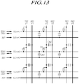
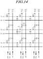
- This embodiment performs self-cap sensing in the first and second period (corresponding figs. 13 , 14 ), and performing mutual-cap sensing in P3 (corresponding figs. 11 ).
- TDS is applied to TE1 and TSS is received from TE2 in P3. That is, according to the embodiment of the present invention, both touch sensing by self-cap sensing and touch sensing by mutual-cap sensing could be performed in mutual-cap sensing touch electrode structure.
- An object is also to provide a method for operating a display device as described above.
- the shield electrode to which a shield electrode driving signal corresponding to the touch driving signal is applied, is disposed between the display electrode and the touch electrodes to remove parasitic capacitance between the display electrode and the touch electrodes, so that display noise in a touch sensing signal can be reduced.
- the accuracy of touch sensing using the touch sensing signal generated based on a change in the self-capacitance of the touch electrodes can be improved.
- both a touch sensing function based on a change in the self-capacitance of the touch electrodes and a touch sensing function based on a change in the mutual capacitance of the touch electrodes can be provided.
- FIG. 1 illustrates a schematic configuration of a touch display device 100 according to exemplary embodiments.
- the touch display device 100 may include a touch display panel 110, a gate driver circuit 120, a data driver circuit 130, and a controller 140.
- the touch display device 100 may include a touch driver circuit 150 to detect a touch made to the touch display panel 110.
- a plurality of gate lines GL and a plurality of data lines DL are disposed in the touch display panel 110.
- a plurality of subpixels, e.g ., SP, are disposed in areas in which the gate lines GL and the data lines DL intersect.
- a plurality of touch electrodes TE may be disposed or embedded in the touch display panel 110, and a plurality of touch lines TL may be disposed in the touch display panel 110 to electrically connect the touch electrodes TE and the touch driver circuit 150.
- the gate driver circuit 120 controls the driving timing of the subpixels SP disposed in the touch display panel 110.
- the data driver circuit 130 supplies data voltages V data , corresponding to image data, to the subpixels SP, so that the subpixels SP represent luminance levels corresponding to grayscales of the image data to display an image.
- the gate driver circuit 120 is controlled by the controller 140.
- the gate driver circuit 120 sequentially outputs a scanning signal to the plurality of gate lines GL disposed in the touch display panel 110 to control the driving timing of the plurality of subpixels SP.
- the gate driver circuit 120 may include one or more gate driver integrated circuits (GDICs) and/or may include one or more processors.
- the GDICs may be disposed on one or both sides of the touch display panel 110, depending on the driving system.
- the gate driver circuit 120 may have a gate-in-panel (GIP) structure embedded in a bezel area of the touch display panel 110.
- GIP gate-in-panel
- the data driver circuit 130 receives image data (or input data) from the controller 140, and converts image data into analog data voltages V data . Then, the data driver circuit 130 outputs the data voltages V data to the data lines DL at points in time at which the scanning signal is applied to the gate lines GL, so that the subpixels SP represent luminance levels corresponding to image data.
- the data driver circuit 130 may include one or more source driver integrated circuits (SDICs) and/or one or more processors.
- SDICs source driver integrated circuits
- the controller 140 supplies a variety of control signals to the gate driver circuit 120 and the data driver circuit 130 to control the operation of the gate driver circuit 120 and the data driver circuit 130.
- the controller 140 controls the gate driver circuit 120 to output a scanning signal at points in time defined by frames.
- the controller 140 converts image data received from an external source into a data signal format readable by the data driver circuit 130, and outputs the converted image data to the data driver circuit 130.
- the controller 140 may receive a variety of timing signals, including a vertical synchronization signal V sync , a horizontal synchronization signal H sync , an input data enable signal DE, and a clock signal CLK, in addition to the image data, from an external source (e.g. a host system).
- a vertical synchronization signal V sync a vertical synchronization signal
- H sync horizontal synchronization signal
- DE input data enable signal
- CLK clock signal
- the controller 140 may generate a variety of control signals using the variety of timing signals received from the external source and output the variety of control signals to the gate driver circuit 120 and the data driver circuit 130.
- the controller 140 outputs a variety of gate control signals, including at least one of a gate start pulse GSP, a gate shift clock GSC, a gate output enable signal GOE, and the like, to control the gate driver circuit 120.
- a gate start pulse GSP a gate start pulse
- GSC a gate shift clock
- GOE gate output enable signal
- the gate start pulse GSP controls the operation start timing of one or more GDICs of the gate circuit 120.
- the gate shift clock GSC is a clock signal commonly input to the one or more GDICs to control the shift timing of scanning signals.
- the gate output enable signal GOE designates timing information of the one or more GDICs.
- the controller 140 outputs a variety of data driving control signals, including at least one of a source start pulse SSP, a source sampling clock SSC, a source output enable signal SOE, and the like, to control the data driver circuit 130.
- the SSP controls the data sampling start timing of one or more SDICs of the data driver 120.
- the source sampling clock SSC is a clock signal controlling the sampling timing of data in each of the SDICs.
- the source output enable signal SOE controls the output timing of the data driver circuit 130.
- the touch display device 100 may further include power management integrated circuit (PMIC) to supply various forms of voltage or current to the organic touch display panel 110, the gate driver circuit 120, the data driver circuit 130, the touch driver circuit 150, and the like, or control various forms of voltage or current to be supplied to the same.
- PMIC power management integrated circuit
- the power management integrated circuit may be integrated into any other circuit of the touch display device 100.
- the subpixels SP are defined by the gate lines GL and the data lines DL intersecting each other.
- Liquid crystal or light-emitting diodes may be disposed in the subpixels, depending on the type of the touch display device 100.
- OLEDs organic light-emitting diodes
- current flowing to the OLEDs may be controlled depending on the data voltage, so that the subpixels SP can represent brightness levels corresponding to the image data.
- the touch display device 100 may detect a user's touch made to the touch display panel 110, using the touch electrodes TE provided in the touch display panel 110 and the touch driver circuit 150.
- FIG. 2 illustrates a structure comprised of touch electrodes TE and a touch driver circuit 150 in the touch display device 100 according to exemplary embodiments, in which the touch electrodes TE are disposed in the touch display panel 110, and the touch driver circuit 150 drives the touch electrodes TE to detect a touch.
- a plurality of touch electrodes TE may be disposed in the touch display panel 110.
- the touch electrodes TE may be disposed on and/or within the touch display panel 110.
- the touch electrodes TE may respectively be a transparent bulk electrode and/or an opaque mesh electrode.
- touch electrodes TE may respectively be a transparent or opaque electrode, and may have an open area, as required. That is, the open area may be present in at least a portion of the touch electrode TE. For example, an open area may be located in a portion of each of the subpixels SP, corresponding to a light-emitting area.
- the touch electrodes TE may be connected to the touch driver circuit 150 via the touch lines TL disposed in the touch display panel 110.
- the touch driver circuit 150 may include a touch sensing circuit connected to the touch electrodes TE via the touch lines TL and a touch controller controlling the touch sensing circuit and detecting an input corresponding to a touch.
- the touch driver circuit 150 may include a touch power circuit supplying a touch driving signal TDS to the touch sensing circuit under the control of the touch controller.
- At least a portion of the touch driver circuit 150 may be integrated with the data driver circuit 130.
- the touch sensing circuit outputs the touch driving signal TDS to the plurality of touch electrodes TE, under the control of the touch controller, and receives touch sensing signals TSS from at least one of the plurality of touch electrodes TE.
- the touch sensing circuit may receive a touch sensing signal TSS from each of the touch electrodes TE via the touch lines TL connected to the touch electrodes TE in a one-to-one relationship.
- the plurality of touch electrodes TE may be separated from each other, and the touch lines TL may be electrically connected to the touch lines TE via contact holes CH, respectively.
- the touch sensing circuit may output a touch driving signal TDS to the touch electrodes TE via the touch lines TL and receive touch sensing signals TSS via the touch lines TL, thereby detecting a change in self-capacitance generated by a touch.
- the touch electrodes may be divided into driving electrodes and sensing electrodes, and the touch sensing circuit may be connected to the driving electrodes and the sensing electrodes.
- the touch sensing circuit may output a touch driving signal TDS to the driving electrodes and receive touch sensing signals TSS from the sensing electrodes, thereby detecting a change in mutual capacitance between the driving electrodes and the sensing electrodes generated by the touch.
- the touch sensing circuit converts a received touch sensing signal TSS into digital sensing data and transfers the converted sensing data to the touch controller.
- the touch controller may receive the sensing data from the touch sensing circuit and detect a user's touch made to the display panel 110, based on the received sensing data, while controlling the operation of the touch sensing circuit.
- the touch controller may detect a change in self-capacitance or a change in mutual capacitance from the sensing data, and based on the detected change in capacitance, determine whether or not the panel has been touched and detect touch coordinates and the like.
- parasitic capacitance Cp may be generated between display driving electrodes, included in the touch display panel 110, and the touch electrodes TE.
- parasitic capacitance Cp may have an effect on touch sensing signals received from the touch electrodes TE.
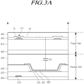
- FIGS. 3A and 3B illustrate cross-sectional structures of portion A-A' of the touch display device 100 illustrated in FIG. 2 , in which parasitic capacitance Cp is generated between a display electrode and a touch electrode TE.
- the touch display device 100 is taken as an organic light-emitting diode (OLED) display device by way of example.
- FIG. 3A illustrates an exemplary structure in which the touch electrode TE is disposed in an on-cell structure
- FIG. 3B illustrates an exemplary structure in which the touch electrode TE is disposed in an in-cell structure.
- a signal line 310 to which a display driving voltage, signal, or the like is applied, may be disposed on a display substrate 300, and a signal line insulating layer 320 may be disposed on the signal line 310.
- a first electrode 330 may be disposed on the signal line insulating layer 320, and a bank 340 defining a light-emitting area may be provided.
- an organic light-emitting layer 350 may be disposed on the first electrode 330, and a second electrode 360 may be disposed on the organic light-emitting layer 350 and the bank 340.
- the first electrode 330 may be an anode, while the second electrode 360 may be a cathode.
- FIG. 3A and 3B illustrate a top emission structure by way of example, in which the second electrode may be a transparent or translucent material.
- the touch display device 100 according to exemplary embodiments may have a bottom emission structure.
- An encapsulation layer 370 may be disposed on the second electrode 360.
- the components, from the display substrate 300 to the encapsulation layer 370, may constitute a display part of the touch display device 100.
- An adhesive layer 400 may be disposed on the display part, and a touch part providing a touch sensing function may be disposed on the adhesive layer 400.
- the touch part may include a touch substrate 410, as well as a touch electrode TE and a touch line TL disposed on the touch substrate 410.
- the touch part may include a touch insulating layer 430, disposed between the touch electrode TE and the touch line TL, and a touch protective layer 440 disposed on the uppermost layer.
- the display panel 110 having touch sensing ability may be provided.
- the touch electrode TE, the touch line TL, and the like may be disposed on the encapsulation layer 370 to provide the touch display panel 110 including an in-cell structure in which the touch electrode TE is disposed.
- a touch buffer layer 420 is disposed on the encapsulation layer 370, and the touch line TL is disposed on the touch buffer layer 420.
- the touch insulating layer 430 is disposed on the touch line TL, and the touch electrode TE is disposed on the touch insulating layer 430.
- the touch electrode TE may be electrically connected to the touch line TL via a contact hole CH formed in the touch insulating layer 430, and the touch protective layer 440 may be disposed on the touch electrode TE.
- the touch display device 100 Since the touch electrode TE and the touch line TL are placed directly on the encapsulation layer 370 as described above, the touch display device 100 able to recognize touches can be easily provided.
- parasitic capacitance Cp may be generated between the second electrode 360, i.e. a display electrode of the display part, located closest to a touched portion, and the touch electrode TE. Such parasitic capacitance Cp may gradually increase with decreases in the thickness of the touch display panel 110.
- parasitic capacitance Cp may cause noise in a touch sensing signal TSS received from the touch electrode TE. Such noise may have an adverse effect on touch sensing performance.
- a change in the self-capacitance of the touch electrode TE is detected during touch recognition, a touch may be erroneously recognized.
- the touch display device 100 can reduce display noise in the touch sensing signal, caused by parasitic capacitance Cp between the display electrode and the touch electrode TE, such that the touch display panel 110 and the touch display device 100 can be designed to have a compact structure while achieving improved accuracy of touch sensing.
- FIG. 4 illustrates a structure for reducing display noise in touch sensing signals TSS in the touch display device 100 according to exemplary embodiments, in which touch electrodes TE for touch sensing and a shield electrode SE for noise reduction are arranged in the touch display panel 110.
- the touch display panel 110 may include a plurality of touch electrodes TE and a plurality of touch lines TL electrically connected to the plurality of touch electrodes TE.
- the touch display panel 110 may further include electrodes, lines, and the like, disposed below the touch electrodes TE and the touch lines TL, and to which display driving voltages and signals are applied.
- the touch display panel 110 may include the shield electrode SE disposed between a display electrode, to which a display driving voltage or the like is applied, and the touch electrodes TE.
- the display electrode may mean an electrode, among electrodes included in the touch display panel 110, located closest to the touch electrodes TE.
- the display electrode is illustrated as a cathode, i.e. the second electrode 360, by way of example.
- the shield electrode SE may be disposed to overlap an area in which the display electrode overlaps the touch electrodes TE.
- the shield electrode SE may overlap an area between two adjacent touch electrodes TE among the plurality of touch electrodes TE.
- the shield electrode may be provided as a bulk electrode between the display electrode and the touch electrodes TE, or may be divided into pieces corresponding to one or more or all of the touch electrodes TE.
- the shield electrode SE may be made of a transparent material or a translucent material, or may be made of the same material as the cathode.
- the shield electrode SE may be made of a material (e.g. indium tin oxide (ITO)) having a certain degree of transparency or higher (e.g. 90% or higher) or a translucent material (e.g. AgMg or a mixture including AgMg).
- ITO indium tin oxide
- the material of the cathode may be the same as the material of the shield electrode SE.
- the shield electrode SE and the cathode may be made of materials having different degrees of transparency.
- the transparency of the shield electrode SE may be higher than the transparency of the cathode.
- a shield signal SS corresponding to the touch driving signal TDS may be applied to the shield electrode SE.
- the shield signal SS corresponding to the touch driving signal TDS may be a signal having the same frequency and phase as the touch driving signal TDS.
- the shield signal SS may be a signal having the same amplitude as the touch driving signal TDS.
- parasitic capacitance Cp can be prevented from being generated directly between the touch electrodes TE and the display electrode.
- parasitic capacitance Cp may be generated between the shield electrode SE, located between the touch electrodes TE overlapping the display electrode, and the display electrode.
- the shield signal SE is applied to the shield electrode SE during the period in which the touch driving signal TDS is applied to the touch electrodes TE, capacitance may not be generated between the touch electrodes TE and the shield electrode SE.
- the shield electrode SE can act to block noise caused by parasitic capacitance Cp that may be generated by the display electrode.
- the shield electrode SE since the shield electrode SE has the shield signal SS, corresponding to the touch driving signal TDS, applied thereto, touch sensing signals TSS received from the touch electrodes TE may not be affected by the shield electrode SE.
- the sensitivity of touch sensing signals TSS, received from the touch electrodes TE may be improved.
- touch sensing signals TSS As display noise in touch sensing signals TSS is reduced and the sensitivity of touch sensing signals TSS is improved, the performance of touch sensing enabled by detecting a self-capacitance change in the touch electrodes TE may be improved.
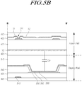
- FIGS. 5A to 5C illustrate cross-sectional structures of portion B-B' of the touch display device 100 illustrated in FIG. 4 .
- FIGS. 5A and 5B illustrate structures respectively including the shield electrode SE disposed in an on-cell structure in which the touch electrode TE is disposed
- FIG. 5C illustrates a structure including the shield electrode SE disposed in an in-cell structure in which the touch electrode TE is disposed.
- the shield electrode SE may be disposed on the encapsulation layer 370 of the display part.
- the adhesive layer 400 may be disposed on the shield electrode SE.
- the touch substrate 410, the touch electrode TE, the touch line TL, and the like may be disposed on the adhesive layer 400.
- the shield electrode SE may be disposed on the encapsulation layer 370 during the processing of the display part.
- the shield electrode SE may constitute the touch part, together with the touch substrate 410, the touch electrode TE, the touch lines TL, and the like, attached to the top of the shield electrode SE via the adhesive layer 400.
- the adhesive layer 400 may be disposed on the encapsulation layer 370 of the display part, and the shield electrode SE may be disposed on the adhesive layer 400.
- the shield electrode SE may be disposed in a variety of locations between the touch electrode TE and the display electrode, depending on the fabrication method, convenience, and the like.
- the shield electrode SE may be disposed in the in-cell structure in which the touch electrode TE is disposed.
- the shield electrode SE may be disposed on the encapsulation layer 370.
- the touch buffer layer 420 may be disposed on the shield electrode SE, and the touch line TL may be disposed on the touch buffer layer 420.
- the touch buffer layer 420 may serve to insulate the shield electrode SE and the touch line TL from each other.
- the touch buffer layer 420 may have a thinner thickness as the thickness of the shield electrode SE.
- the touch insulating layer 430, the touch electrode TE, and the touch protective layer 440 may be disposed on the touch line TL.
- the touch display device 100 having a touch sensing function, with the shield electrode SE being disposed between the touch electrode TE and the display electrode, can easily be provided.
- the shield electrode SE is disposed between the second electrode 360, i.e. the display electrode closest to the touch electrode TE, and the touch electrode TE in the display part, parasitic capacitance Cp can be prevented from being generated between the second electrode 360 and the touch electrode TE.
- the shield electrode SE can block display noise to improve the sensitivity of a touch sensing signal TSS received from the touch electrode TE.
- the touch electrode TE and the touch line TL can be disposed in a more variety of structures.
- FIGS. 6A to 6C illustrate other cross-sectional structures of portion B-B' of the touch display device 100 illustrated in FIG. 4 .
- FIGS. 6A and 6B illustrate structures in each of which the shield electrode SE is disposed in an on-cell structure
- FIG. 6C illustrates a structure in which the shield electrode SE is disposed in an in-cell structure.
- the touch electrode TE is disposed on the touch substrate 410, and the touch insulating layer 430 is disposed on the touch electrode TE.
- the touch line TL is disposed on the touch insulating layer 430, and the touch protective layer 440 is disposed on the touch line TL.
- the touch line TL may be electrically connected to the touch electrode TE via the contact hole CH provided in the touch insulating layer 430.
- the touch electrode TE may be located closer to the display electrode.
- the touch electrode TE having a wider area than the touch line TL, may be disposed below the touch line TL, and the touch line TL and the touch electrode TE may be electrically connected to each other via the contact hole CH, such that the contacting between the touch line TL and the touch electrode TE can be more easily performed.
- the touch line TL may be located above the touch electrode TE.
- the shield electrode SE is disposed on the encapsulation layer 470, and the touch buffer layer 420 is disposed on the shield electrode SE.
- the touch electrode TE may be disposed on the touch buffer layer 420, and the shield electrode SE and the touch electrode TE may be insulated from each other via the touch buffer layer 420.
- the touch insulating layer 430 and the touch line TL may be disposed on the touch electrode TE, and the touch line TL may be electrically connected to the touch electrode TE via the contact hole CH provided in the touch insulating layer 430.
- the shield electrode SE is disposed between the touch electrode and the display electrode to block display noise, the position of the touch electrode TE may be selected more variously. Accordingly, the touch electrode TE and the touch line TL may be disposed in a greater variety of structures, in consideration of the convenience of design and the like.
- the touch display device 100 may further include a shield line SL to supply a shield signal SS to the shield electrode SE, as required.
- the shield line SL is disposed to overlap the shield electrode SE and the like.
- FIG. 7 illustrates another arrangement structure of touch electrodes TE and a shield electrode SE in the touch display device 100 according to exemplary embodiments.
- the touch display device 100 includes the shield electrode SE disposed between the touch electrode TE and the display electrode.
- the touch display device 100 may also include the plurality of touch lines TL electrically connected to the touch electrodes TE, respectively, and a plurality of shield lines SL electrically connected to the shield electrode SE.
- Each of the plurality of touch lines TL is electrically connected to a corresponding electrode TE of the touch electrodes TE via at least one first contact hole CH1.
- each of the plurality of touch lines TL applies a touch driving signal TDS, output from the touch driver circuit 150, to the corresponding touch electrode TE, and transfers a touch sensing signal TSS to the touch driver circuit 150.
- the plurality of shield lines SL are electrically connected to the shield electrode SE via at least one second contact hole CH2.
- This configuration may allow a shield signal SS, output from the touch driver circuit 150 or an additional driver circuit, to be applied to the shield electrode SE.
- the shape or profile of at least a portion of each of the touch electrodes TE may be modified to form the second contact hole CH.
- the second contact holes CH2 may be formed in the other locations, except for the areas in which the touch electrodes TE are disposed, without the modification of the shape of the touch electrodes TE, such that the shield signal SS can be applied to the shield electrode SE.
- the shield lines SL may be disposed on the same layer as the touch lines TL, and may be insulated from the touch lines TL and the touch electrodes TL.
- the shield electrode SE may receive the shield signal SS via lines disposed in the periphery of the touch display panel 110, or as illustrated in FIG. 7 , via the shield lines SL disposed to overlap the shield electrode SE.
- the shield signal SS may be applied to the shield electrode SE during a period in which the touch driving signal TDS is applied to the touch electrodes TE, such that the shield electrode SE can block display noise without affecting the touch sensing signal TSS.
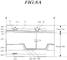
- FIGS. 8A and 8B illustrate cross-sectional structures of portion C-C' of the touch display device 100 illustrated in FIG. 7 , in each of which the touch electrode TE is disposed in an on-cell structure.
- the shield electrode SE is disposed on the encapsulation layer 370, and the touch buffer layer 420 is disposed on the shield electrode SE.
- the touch electrode TE is disposed on the touch buffer layer 420, and the touch insulating layer 430 is disposed on the touch electrode TE.
- the touch line TL and the shield line SL may be disposed on the touch insulating layer 430, and the touch protective layer 440 may be disposed on the touch line TL and the shield line SL.
- the touch line TL and the shield line SL may be disposed on the same layer, and be made of the same material.
- the touch line TL may be electrically connected to the touch electrode TE via the first contact hole CH1
- the shield line SL may be electrically connected to the shield electrode SE via the second contact hole CH2 formed in the touch buffer layer 420 and the touch insulating layer 430.
- the shield line SL electrically connected to the shield electrode SE to apply the shield signal SS to the shield electrode SE, may be easily disposed.
- the touch line TL and the shield line SL may be disposed between the touch electrode TE and the shield electrode SE.
- the shield electrode SE is disposed directly on the encapsulation layer 370, and the touch buffer layer 420 is disposed directly on the shield electrode SE.
- the touch line TL and the shield line SL are disposed directly on the touch buffer layer 420, and the touch insulating layer 430 is disposed directly on the touch line TL and the shield line SL.
- the touch electrode TE is disposed directly on the touch insulating layer 430.
- the touch line TL and the shield line SL may be disposed on the same layer, between the touch electrode TE and the shield electrode SE.
- the touch line TL and the touch electrode TE may be electrically connected to each other via the first contact hole CH1 formed in the touch insulating layer 430, and the shield line SL and the shield electrode SE may be electrically connected to each other via the second contact hole CH2 formed in the touch buffer layer 420.
- the touch line TL and the shield line SL are disposed between the touch electrode TE and the shield electrode SE as described above, the area of the touch electrode TE to be reduced by the second contact hole CH2 connecting the shield line SL and the shield electrode SE can be minimized.
- the structures of the touch electrode TE for sensing a touch by detecting a change in self-capacitance have been illustrated in the foregoing exemplary embodiments, the same may be applied to the structures of the touch electrode TE for sensing a touch by detecting a change in mutual capacitance.
- FIG. 9 illustrates another arrangement structure of touch electrodes TE and shield electrodes SE in the touch display device 100 according to exemplary embodiments.
- the touch display device 100 may include the plurality of touch electrodes TE and the plurality of shield electrodes SE disposed between the plurality of touch electrodes TE and the display electrode.
- the plurality of touch electrodes TE may include a plurality of first touch electrodes TE1 connected to each other in a first direction and a plurality of second touch electrodes TE2 connected to each other in a second direction.
- the touch display device 100 may also include a first touch electrode connecting pattern TE_CP1 comprised of one or more pattern elements respectively connecting two adjacent first touch electrodes TE1 among the plurality of first touch electrodes TE1 and a second touch electrode connecting pattern TE_CP2 comprised of one or more pattern elements respectively connecting two adjacent second touch electrodes TE2 among the plurality of second touch electrodes TE2.
- TE_CP1 comprised of one or more pattern elements respectively connecting two adjacent first touch electrodes TE1 among the plurality of first touch electrodes TE1
- a second touch electrode connecting pattern TE_CP2 comprised of one or more pattern elements respectively connecting two adjacent second touch electrodes TE2 among the plurality of second touch electrodes TE2.
- first touch electrode connecting pattern TE_CP1 and the second touch electrode connecting pattern TE_CP2 may be disposed on different layers.
- the pattern elements of the second touch electrode connecting pattern TE_CP2 may be disposed on the same layer as the first touch electrodes TE1 and the second touch electrodes TE2, and respectively connect two adjacent second touch electrodes TE2.
- the pattern elements of the first touch electrode connecting pattern TE_CP1 may be disposed on different layers from the first touch electrodes TE1 and the second touch electrodes TE2, and respectively connect two adjacent first touch electrodes TE1 to each other via contact holes CH3 and CH4.
- the plurality of shield electrodes SE may include a plurality of first shield electrodes SE1 disposed to correspond to the plurality of first touch electrodes TE1, respectively, and a plurality of second shield electrodes SE2 disposed to correspond to the plurality of second touch electrodes TE2, respectively.
- the area of the first shield electrode SE1 and the area of the second shield electrode SE2 may be greater than the area of the first touch electrode TE1 and the area of the second touch electrode TE2, respectively.
- the plurality of first shield electrodes SE1 may be connected to each other in the same first direction as the first touch electrodes TE1, and the plurality of second shield electrodes SE2 may be connected to each other in the same second direction as the first touch electrodes TE2.
- the touch display device 100 may also include a first shield electrode connecting pattern SE_CP1 comprised of one or more pattern elements respectively connecting two adjacent first shield electrodes SE1 and a second shield electrode connecting pattern SE_CP2 comprised of one or more pattern elements respectively connecting two adjacent second shield electrodes SE2.
- the first shield electrode connecting pattern SE_CP1 and the second shield electrode connecting pattern SE_CP2 may be disposed on the different layers.
- the pattern elements of the second shield electrode connecting pattern SE_CP2 may be disposed on the same layer as the first shield electrodes SE1 and the second shield electrodes SE2, and respectively connect two adjacent second shield electrodes SE2.
- the pattern elements of the first shield electrode connecting pattern SE_CP1 may be disposed on different layers from the first shield electrodes SE1 and the second shield electrodes SE2, and respectively connect two adjacent first shield electrodes SE1 to each other via contact holes CH5 and CH6.
- some portions of the patterns connecting the shield electrode SE may be disposed to overlap the patterns connecting the touch electrode TE, and other portions of the patterns connecting the shield electrode SE may be disposed on the same layer as overlap the patterns connecting the touch electrode TE.
- the first touch electrode connecting pattern TE_CP1 and the first shield electrode connecting pattern SE_CP1 may be disposed on the same layer, and they may be disposed on separate layers.
- the second touch electrode connecting pattern TE_CP2 and the second shield electrode connecting pattern SE_CP2 may be disposed to overlap each other.
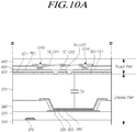
- FIGS. 10A and 10B illustrate cross-sectional structures of portions of the touch display device 100 illustrated in FIG. 9 , in which the touch electrode connecting patterns TE_CP and the shield electrode connecting patterns SE_CP are disposed.
- FIG. 10A illustrates the cross-sectional structure of portion D-D' in which the first touch electrode connecting pattern TE_CP1 is disposed
- FIG. 10B illustrates the cross-sectional structure of portion E-E' in which the first shield electrode connecting pattern SE_CP1 is disposed.
- the first shield electrodes SE1 and the second electrodes SE2 are disposed on the encapsulation layer 370.
- the second shield electrode connecting pattern SE_CP2 connecting two adjacent second shield electrodes SE2 is disposed on the encapsulation layer 370.
- the touch buffer layer 420 is disposed on the first shield electrodes SE1 and the second shield electrodes SE2.
- the first touch electrodes TE1 and the second touch electrodes TE2 are disposed on the touch buffer layer 420.
- the second touch electrode connecting pattern TE_CP2 connecting two adjacent second touch electrodes TE2 is disposed on the touch buffer layer 420.
- the touch insulating layer 430 is disposed on the first touch electrodes TE1 and the second touch electrodes TE2, and the first touch electrode connecting pattern TE_CP1 is disposed on the touch insulating layer 430.
- the pattern elements of the first touch electrode connecting pattern TE_CP1 may respectively connect two adjacent first touch electrodes TE1 to each other via the third contact hole CH3 and the fourth contact hole CH4 formed in the touch insulating layer 430.
- the touch protective layer 440 is disposed on the first touch electrode connecting pattern TE_CP1.
- the first shield electrode connecting pattern SE_CP1 may be disposed on the same layer as the first touch electrode connecting pattern TE_CP1.
- the first shield electrode connecting pattern SE_CP1 is disposed on the touch insulating layer 430.
- the pattern elements of the first shield electrode connecting pattern SE_CP1 may respectively connect two adjacent first shield electrodes SE1 to each other via the fifth contact hole CH5 and the sixth contact hole CH6 formed in the touch buffer layer 420 and the touch insulating layer 430.
- first shield electrodes SE1 and the second shield electrodes SE2 are disposed in positions corresponding to the first touch electrodes TE1 and the second touch electrodes TE2 as described above, parasitic capacitance Cp between the touch electrode TE and the display electrode can be prevented, and the touch sensing signal TSS can be protected from display noise.
- first shield electrodes SE1 and the second shield electrodes SE2 are disposed using the same connecting structures as those of the first touch electrodes TE1 and the second touch electrodes TE2, touch driving in which display noise is blocked using the shield electrode SE can be provided.
- FIGS. 11 and 12 illustrate a driving method of the touch display device 100 illustrated in FIG. 9 , in which a touch is sensed by detecting mutual capacitance between the first touch electrodes TE1 and the second touch electrodes TE2.
- the touch driver circuit 150 outputs a touch driving signal TDS to the first touch electrodes TE1 and outputs a shield signal SS, corresponding to the touch driving signal TDS, to the first shield electrodes SE1.
- the touch driver circuit 150 controls the second touch electrodes TE2 and the second shield electrode SE2 to maintain the same constant voltage state.
- the second touch electrodes TE2 and the second shield electrode SE2 may maintain a touch sensing reference voltage applied thereto.
- the touch driver circuit 150 may perform touch sensing based on mutual capacitance by receiving touch sensing signals TSS from the second touch electrodes TE2 and detecting mutual capacitance between the first touch electrodes TE1 and the second touch electrodes TE2.
- display noise can be prevented from being caused by parasitic capacitance Cp generated by the display electrode, so that touch sensing based on a change in the mutual capacitance of the touch electrodes TE can be performed.
- touch sensing based on a change in the self-capacitance of the touch electrodes TE can be performed.
- FIGS. 13 to 15 illustrate another driving method of the touch display device 100 illustrated in FIG. 9 , in which a touch is sensed by detecting self-capacitance of the first touch electrodes TE1 and self-capacitance of the second touch electrodes TE2.
- the touch driver circuit 150 outputs a first driving signal TDS1 to the first touch electrodes TE1, and outputs a first shield signal SS1, corresponding to the first driving signal TDS1, to the first shield electrodes SE1.
- the touch driver circuit 150 may detect a change in the self-capacitance of the first touch electrodes TE1 by receiving first touch sensing signals TSS1 from the first touch electrodes TE1.
- the first shield electrodes SE1 are disposed to correspond to the first touch electrodes TE1 to block display noise, so that the sensitivity of detection of a change in the self-capacitance of the first touch electrodes TE1 can be improved.
- the touch driver circuit 150 outputs a second driving signal TDS2 to the second touch electrodes TE2, and outputs a second shield signal SS2, corresponding to the second driving signal TDS2, to the second shield electrodes SE2.
- the touch driver circuit 150 may detect a change in the self-capacitance of the second touch electrodes TE2 by receiving second touch sensing signals TSS2 from the second touch electrodes TE2.
- the second shield electrodes SE2 serve to block display noise, so that the sensitivity of detection of a change in the self-capacitance of the second touch electrodes TE2 can be improved.
- the touch driver circuit 150 can sense a user's touch made to the touch display panel 110, based on a change in the self-capacitance of the first touch electrodes TE1, detected in the first period PI, and a change in the self-capacitance of the second touch electrodes TE2, detected in the second period P2.
- touch sensing can be performed by detecting the self-capacitance of each of the first touch electrodes TE1 and the second touch electrodes TE2.
- touch sensing can be performed based on self-capacitance sensing and mutual capacitance sensing, as required.
- FIG. 16 illustrates a driving method of the touch driver circuit 150 according to exemplary embodiments.
- the touch driver circuit 150 drives the first touch electrodes TE1 and the first shield electrodes SE1 corresponding to the first touch electrodes TE1 during a first period P1.
- the touch driver circuit 150 receives first touch sensing signals TSS1 from the first touch electrodes TE1.
- the touch driver circuit 150 drives the second touch electrodes TE2 and the second shield electrodes SE2 corresponding to the second touch electrodes TE2 during a second period P2.
- the touch driver circuit 150 receives second touch sensing signals TSS2 from the second touch electrodes TE2.
- the touch driver circuit 150 detects a user's touch based on the first touch sensing signals TSS1 and the second touch sensing signals TSS2.
- the touch driver circuit 150 may perform touch sensing based on a change in mutual capacitance by simultaneously driving the first touch electrodes TE1 and the second touch electrodes TE2.
- the first shield electrodes SE1 and the second shield electrodes SE2 may be driven to correspond to the first touch electrodes TE1 and the second touch electrodes TE2.
- the shield electrodes SE are disposed between the display electrode and the touch electrodes TE, and a signal, corresponding to a signal applied to the touch electrodes TE, is applied to the shield electrode SE, so that the shield electrodes SE can block display noise to improve the sensitivity of touch sensing signals TSS received from the touch electrodes TE.
- the removal of display noise can improve the accuracy of detection of a change in the self-capacitance of the touch electrodes TE, thereby improving touch sensing performance based on the change in the self-capacitance.
- both the touch sensing function based on the detection of self-capacitance and the touch sensing function based on the detection of mutual capacitance can be provided. Accordingly, touch sensing can be provided, based on at least one of the detection of self-capacitance and the detection of mutual capacitance, as required.
Landscapes
- Engineering & Computer Science (AREA)
- General Engineering & Computer Science (AREA)
- Theoretical Computer Science (AREA)
- Physics & Mathematics (AREA)
- Human Computer Interaction (AREA)
- General Physics & Mathematics (AREA)
- Computer Networks & Wireless Communication (AREA)
- Optics & Photonics (AREA)
- Microelectronics & Electronic Packaging (AREA)
- Acoustics & Sound (AREA)
- Devices For Indicating Variable Information By Combining Individual Elements (AREA)
- Electroluminescent Light Sources (AREA)
- Position Input By Displaying (AREA)
- Liquid Crystal (AREA)
Applications Claiming Priority (1)
| Application Number | Priority Date | Filing Date | Title |
|---|---|---|---|
| KR1020180075651A KR102553525B1 (ko) | 2018-06-29 | 2018-06-29 | 터치 디스플레이 패널, 터치 디스플레이 장치 |
Publications (1)
| Publication Number | Publication Date |
|---|---|
| EP3588253A1 true EP3588253A1 (fr) | 2020-01-01 |
Family
ID=67137536
Family Applications (1)
| Application Number | Title | Priority Date | Filing Date |
|---|---|---|---|
| EP19183043.9A Ceased EP3588253A1 (fr) | 2018-06-29 | 2019-06-27 | Panneau d'affichage tactile et dispositif d'affichage tactile |
Country Status (4)
| Country | Link |
|---|---|
| US (1) | US10908721B2 (fr) |
| EP (1) | EP3588253A1 (fr) |
| KR (1) | KR102553525B1 (fr) |
| CN (1) | CN110658943B (fr) |
Families Citing this family (20)
| Publication number | Priority date | Publication date | Assignee | Title |
|---|---|---|---|---|
| CN208580390U (zh) * | 2018-07-27 | 2019-03-05 | 深圳市汇顶科技股份有限公司 | 电容式触摸屏模组及电子终端 |
| JP7383869B2 (ja) * | 2020-02-13 | 2023-11-21 | シャープ株式会社 | タッチパネル及び表示装置 |
| CN113467630B (zh) * | 2020-03-31 | 2024-11-12 | 京东方科技集团股份有限公司 | 阵列基板及其制作方法和触控显示装置 |
| CN111708464B (zh) * | 2020-06-30 | 2022-09-09 | 厦门天马微电子有限公司 | 触控显示面板和触控显示装置 |
| US11574967B2 (en) * | 2020-08-14 | 2023-02-07 | Novatek Microelectronics Corp. | Organic light-emitting display panel |
| CN112114702B (zh) * | 2020-09-08 | 2023-05-30 | 武汉华星光电半导体显示技术有限公司 | 显示面板及其制作方法 |
| KR102818015B1 (ko) * | 2020-12-24 | 2025-06-11 | 엘지디스플레이 주식회사 | 터치 디스플레이 장치 |
| KR102829726B1 (ko) * | 2020-12-29 | 2025-07-04 | 엘지디스플레이 주식회사 | 터치 디스플레이 장치 |
| CN112578947B (zh) * | 2021-01-12 | 2025-01-10 | 新阳荣乐(上海)汽车电子有限公司 | 一种Incell断码触摸显示屏ITO的设计结构 |
| US12524102B2 (en) * | 2021-03-01 | 2026-01-13 | Sharp Kabushiki Kaisha | Display device |
| CN113629204A (zh) * | 2021-06-25 | 2021-11-09 | 荣耀终端有限公司 | 显示面板及其制造方法、电子设备 |
| CN113467639B (zh) * | 2021-06-30 | 2023-05-23 | 合肥维信诺科技有限公司 | 一种触控面板及触控显示装置 |
| KR102926587B1 (ko) * | 2021-07-05 | 2026-02-13 | 엘지디스플레이 주식회사 | 터치 디스플레이 장치 |
| KR20230026561A (ko) * | 2021-08-17 | 2023-02-27 | 삼성디스플레이 주식회사 | 전자 장치 |
| US11960680B2 (en) * | 2021-11-03 | 2024-04-16 | Samsung Electronics Co., Ltd. | Touch controller, operating method of the same, and touch sensing device including touch controller |
| KR20230087188A (ko) * | 2021-12-09 | 2023-06-16 | 엘지디스플레이 주식회사 | 터치 디스플레이 장치 |
| KR20230088976A (ko) * | 2021-12-13 | 2023-06-20 | 엘지디스플레이 주식회사 | 터치 디스플레이 장치 |
| KR20240107982A (ko) * | 2022-12-30 | 2024-07-09 | 엘지디스플레이 주식회사 | 표시 장치 |
| KR20250125600A (ko) * | 2024-02-15 | 2025-08-22 | 엘지디스플레이 주식회사 | 터치 표시 장치 |
| US12561029B2 (en) * | 2024-07-30 | 2026-02-24 | Pixart Imaging Inc. | Touch panel |
Citations (6)
| Publication number | Priority date | Publication date | Assignee | Title |
|---|---|---|---|---|
| EP2267791A2 (fr) * | 2008-01-29 | 2010-12-29 | Melfas | Appareil tactile présentant une structure de prévention de la capacité parasite |
| US20160132148A1 (en) * | 2014-11-06 | 2016-05-12 | Samsung Display Co., Ltd. | Organic light-emitting diode (oled) display |
| US20160154499A1 (en) * | 2014-11-28 | 2016-06-02 | Samsung Display Co., Ltd. | Display device including touch sensing sensor |
| US20170329444A1 (en) * | 2014-12-05 | 2017-11-16 | Lg Display Co., Ltd. | Display device having integral self-capacitance touch sensor |
| US20180145114A1 (en) * | 2016-11-21 | 2018-05-24 | Lg Display Co., Ltd. | Display Device Including Touch Electrode |
| KR20180075651A (ko) | 2015-12-02 | 2018-07-04 | 콘티넨탈 테베스 아게 운트 코. 오하게 | 브레이크 압력 제어 유닛 |
Family Cites Families (15)
| Publication number | Priority date | Publication date | Assignee | Title |
|---|---|---|---|---|
| US8237068B2 (en) * | 2009-08-07 | 2012-08-07 | OpeanPeak Inc. | Projected capacitive touch-sensitive panel |
| KR101686108B1 (ko) * | 2010-09-28 | 2016-12-14 | 엘지디스플레이 주식회사 | 터치 패널 일체형 표시 장치 |
| CN102541339A (zh) * | 2010-12-29 | 2012-07-04 | 东莞万士达液晶显示器有限公司 | 触控显示装置 |
| CN102937845B (zh) * | 2012-10-26 | 2015-12-02 | 北京京东方光电科技有限公司 | 一种内嵌式触摸屏及显示装置 |
| JP2014164327A (ja) * | 2013-02-21 | 2014-09-08 | Toppan Printing Co Ltd | タッチセンサ、タッチパネル、および、表示装置 |
| KR102078650B1 (ko) * | 2013-09-13 | 2020-02-18 | 엘지디스플레이 주식회사 | 터치 ic 및 이를 이용한 터치 스크린 표시장치 |
| KR102189313B1 (ko) * | 2013-11-28 | 2020-12-10 | 삼성디스플레이 주식회사 | 표시 장치 |
| CN104035615B (zh) * | 2014-05-20 | 2016-03-02 | 京东方科技集团股份有限公司 | 一种触摸显示面板和显示装置 |
| CN104020913A (zh) * | 2014-05-30 | 2014-09-03 | 京东方科技集团股份有限公司 | 一种内嵌式触摸屏及显示装置 |
| US9632638B2 (en) * | 2014-09-10 | 2017-04-25 | Synaptics Incorporated | Device and method for force and proximity sensing employing an intermediate shield electrode layer |
| US10168844B2 (en) * | 2015-06-26 | 2019-01-01 | Samsung Display Co., Ltd. | Flexible display device |
| TWI581169B (zh) * | 2016-04-28 | 2017-05-01 | 友達光電股份有限公司 | 雙模式電容觸控顯示面板 |
| KR102714659B1 (ko) * | 2016-12-09 | 2024-10-07 | 엘지디스플레이 주식회사 | 전자 기기 |
| TWI621049B (zh) * | 2017-06-08 | 2018-04-11 | 友達光電股份有限公司 | 觸控面板 |
| US10452201B1 (en) * | 2018-03-30 | 2019-10-22 | Sharp Kabushiki Kaisha | Touch sensor for display with shield |
-
2018
- 2018-06-29 KR KR1020180075651A patent/KR102553525B1/ko active Active
-
2019
- 2019-06-27 EP EP19183043.9A patent/EP3588253A1/fr not_active Ceased
- 2019-06-27 US US16/455,206 patent/US10908721B2/en active Active
- 2019-06-28 CN CN201910575854.5A patent/CN110658943B/zh active Active
Patent Citations (6)
| Publication number | Priority date | Publication date | Assignee | Title |
|---|---|---|---|---|
| EP2267791A2 (fr) * | 2008-01-29 | 2010-12-29 | Melfas | Appareil tactile présentant une structure de prévention de la capacité parasite |
| US20160132148A1 (en) * | 2014-11-06 | 2016-05-12 | Samsung Display Co., Ltd. | Organic light-emitting diode (oled) display |
| US20160154499A1 (en) * | 2014-11-28 | 2016-06-02 | Samsung Display Co., Ltd. | Display device including touch sensing sensor |
| US20170329444A1 (en) * | 2014-12-05 | 2017-11-16 | Lg Display Co., Ltd. | Display device having integral self-capacitance touch sensor |
| KR20180075651A (ko) | 2015-12-02 | 2018-07-04 | 콘티넨탈 테베스 아게 운트 코. 오하게 | 브레이크 압력 제어 유닛 |
| US20180145114A1 (en) * | 2016-11-21 | 2018-05-24 | Lg Display Co., Ltd. | Display Device Including Touch Electrode |
Also Published As
| Publication number | Publication date |
|---|---|
| KR20200002299A (ko) | 2020-01-08 |
| US20200004368A1 (en) | 2020-01-02 |
| CN110658943A (zh) | 2020-01-07 |
| KR102553525B1 (ko) | 2023-07-10 |
| US10908721B2 (en) | 2021-02-02 |
| CN110658943B (zh) | 2023-05-12 |
Similar Documents
| Publication | Publication Date | Title |
|---|---|---|
| EP3588253A1 (fr) | Panneau d'affichage tactile et dispositif d'affichage tactile | |
| KR101762523B1 (ko) | 터치 패널, 터치 패널의 터치 위치결정 방법 및 디스플레이 디바이스 | |
| EP3291063B1 (fr) | Afficheur comprenant un écran tactile intégré et procédé de commande | |
| EP3299940B1 (fr) | Panneau d'affichage électroluminescent organique et afficheur électroluminescent organique intégrant un écran tactile | |
| KR101315227B1 (ko) | 터치스크린 일체형 표시장치 및 그 구동 방법 | |
| KR101570455B1 (ko) | 터치스크린 일체형 표시장치 및 그 구동 방법 | |
| US10082907B2 (en) | Driving circuit, touch display device, and method of driving the touch display device | |
| EP4009374A1 (fr) | Dispositif d'affichage comprenant une unité de détection tactile | |
| CN110941360A (zh) | 触摸显示装置 | |
| US11275462B2 (en) | Touch display device | |
| KR101733728B1 (ko) | 터치스크린 일체형 표시장치 | |
| CN109766021B (zh) | 电致发光显示装置及其制造方法 | |
| US12069916B2 (en) | Touch display device with short circuit prevention electrode | |
| JP2017134249A (ja) | 表示装置 | |
| KR102436563B1 (ko) | 표시장치 | |
| KR20180046865A (ko) | 터치 센서 내장형 전계발광 표시장치 | |
| US20240103669A1 (en) | Pixelated mutual capacitance sensing for water detection | |
| TW202244713A (zh) | 觸控電路、顯示觸控系統、觸控面板和觸控感測方法 | |
| KR20160094172A (ko) | 스타일러스 펜을 이용한 평판표시장치 | |
| KR101720997B1 (ko) | 터치스크린 일체형 표시장치 | |
| KR20170033485A (ko) | 터치 스크린 패널을 포함하는 유기발광 다이오드 표시장치 및 그 구동방법 | |
| KR20170062646A (ko) | 터치 스크린 패널 및 이를 포함하는 표시장치 | |
| KR101688428B1 (ko) | 디스플레이 드라이버 ic, 터치스크린 일체형 표시장치 및 그 구동 방법 | |
| US20230185413A1 (en) | Touch Display Device | |
| KR102527732B1 (ko) | 터치 회로, 터치 디스플레이 장치 및 그 구동 방법 |
Legal Events
| Date | Code | Title | Description |
|---|---|---|---|
| PUAI | Public reference made under article 153(3) epc to a published international application that has entered the european phase |
Free format text: ORIGINAL CODE: 0009012 |
|
| STAA | Information on the status of an ep patent application or granted ep patent |
Free format text: STATUS: REQUEST FOR EXAMINATION WAS MADE |
|
| 17P | Request for examination filed |
Effective date: 20190627 |
|
| AK | Designated contracting states |
Kind code of ref document: A1 Designated state(s): AL AT BE BG CH CY CZ DE DK EE ES FI FR GB GR HR HU IE IS IT LI LT LU LV MC MK MT NL NO PL PT RO RS SE SI SK SM TR |
|
| AX | Request for extension of the european patent |
Extension state: BA ME |
|
| RBV | Designated contracting states (corrected) |
Designated state(s): AL AT BE BG CH CY CZ DE DK EE ES FI FR GB GR HR HU IE IS IT LI LT LU LV MC MK MT NL NO PL PT RO RS SE SI SK SM TR |
|
| STAA | Information on the status of an ep patent application or granted ep patent |
Free format text: STATUS: EXAMINATION IS IN PROGRESS |
|
| 17Q | First examination report despatched |
Effective date: 20210818 |
|
| STAA | Information on the status of an ep patent application or granted ep patent |
Free format text: STATUS: THE APPLICATION HAS BEEN REFUSED |
|
| 18R | Application refused |
Effective date: 20230425 |