EP3594997A1 - Herstellungsverfahren von mindestens einer halbleiterstruktur, die eine abscheidungsphase gegenüber dem wachstumssubstrat umfasst - Google Patents
Herstellungsverfahren von mindestens einer halbleiterstruktur, die eine abscheidungsphase gegenüber dem wachstumssubstrat umfasst Download PDFInfo
- Publication number
- EP3594997A1 EP3594997A1 EP19185598.0A EP19185598A EP3594997A1 EP 3594997 A1 EP3594997 A1 EP 3594997A1 EP 19185598 A EP19185598 A EP 19185598A EP 3594997 A1 EP3594997 A1 EP 3594997A1
- Authority
- EP
- European Patent Office
- Prior art keywords
- nucleation layer
- support substrate
- semiconductor structure
- electrode
- semiconductor
- Prior art date
- Legal status (The legal status is an assumption and is not a legal conclusion. Google has not performed a legal analysis and makes no representation as to the accuracy of the status listed.)
- Granted
Links
Images

Classifications
-
- H—ELECTRICITY
- H10—SEMICONDUCTOR DEVICES; ELECTRIC SOLID-STATE DEVICES NOT OTHERWISE PROVIDED FOR
- H10P—GENERIC PROCESSES OR APPARATUS FOR THE MANUFACTURE OR TREATMENT OF DEVICES COVERED BY CLASS H10
- H10P95/00—Generic processes or apparatus for manufacture or treatments not covered by the other groups of this subclass
- H10P95/11—Separation of active layers from substrates
-
- H—ELECTRICITY
- H10—SEMICONDUCTOR DEVICES; ELECTRIC SOLID-STATE DEVICES NOT OTHERWISE PROVIDED FOR
- H10P—GENERIC PROCESSES OR APPARATUS FOR THE MANUFACTURE OR TREATMENT OF DEVICES COVERED BY CLASS H10
- H10P14/00—Formation of materials, e.g. in the shape of layers or pillars
- H10P14/20—Formation of materials, e.g. in the shape of layers or pillars of semiconductor materials
- H10P14/32—Formation of materials, e.g. in the shape of layers or pillars of semiconductor materials characterised by intermediate layers between substrates and deposited layers
- H10P14/3202—Materials thereof
- H10P14/3214—Materials thereof being Group IIIA-VA semiconductors
- H10P14/3216—Nitrides
-
- H—ELECTRICITY
- H10—SEMICONDUCTOR DEVICES; ELECTRIC SOLID-STATE DEVICES NOT OTHERWISE PROVIDED FOR
- H10H—INORGANIC LIGHT-EMITTING SEMICONDUCTOR DEVICES HAVING POTENTIAL BARRIERS
- H10H20/00—Individual inorganic light-emitting semiconductor devices having potential barriers, e.g. light-emitting diodes [LED]
- H10H20/01—Manufacture or treatment
- H10H20/011—Manufacture or treatment of bodies, e.g. forming semiconductor layers
- H10H20/013—Manufacture or treatment of bodies, e.g. forming semiconductor layers having light-emitting regions comprising only Group III-V materials
- H10H20/0133—Manufacture or treatment of bodies, e.g. forming semiconductor layers having light-emitting regions comprising only Group III-V materials with a substrate not being Group III-V materials
- H10H20/01335—Manufacture or treatment of bodies, e.g. forming semiconductor layers having light-emitting regions comprising only Group III-V materials with a substrate not being Group III-V materials the light-emitting regions comprising nitride materials
-
- H—ELECTRICITY
- H10—SEMICONDUCTOR DEVICES; ELECTRIC SOLID-STATE DEVICES NOT OTHERWISE PROVIDED FOR
- H10H—INORGANIC LIGHT-EMITTING SEMICONDUCTOR DEVICES HAVING POTENTIAL BARRIERS
- H10H20/00—Individual inorganic light-emitting semiconductor devices having potential barriers, e.g. light-emitting diodes [LED]
- H10H20/01—Manufacture or treatment
- H10H20/011—Manufacture or treatment of bodies, e.g. forming semiconductor layers
- H10H20/013—Manufacture or treatment of bodies, e.g. forming semiconductor layers having light-emitting regions comprising only Group III-V materials
- H10H20/0137—Manufacture or treatment of bodies, e.g. forming semiconductor layers having light-emitting regions comprising only Group III-V materials the light-emitting regions comprising nitride materials
-
- H—ELECTRICITY
- H10—SEMICONDUCTOR DEVICES; ELECTRIC SOLID-STATE DEVICES NOT OTHERWISE PROVIDED FOR
- H10H—INORGANIC LIGHT-EMITTING SEMICONDUCTOR DEVICES HAVING POTENTIAL BARRIERS
- H10H20/00—Individual inorganic light-emitting semiconductor devices having potential barriers, e.g. light-emitting diodes [LED]
- H10H20/01—Manufacture or treatment
- H10H20/011—Manufacture or treatment of bodies, e.g. forming semiconductor layers
- H10H20/018—Bonding of wafers
-
- H—ELECTRICITY
- H10—SEMICONDUCTOR DEVICES; ELECTRIC SOLID-STATE DEVICES NOT OTHERWISE PROVIDED FOR
- H10P—GENERIC PROCESSES OR APPARATUS FOR THE MANUFACTURE OR TREATMENT OF DEVICES COVERED BY CLASS H10
- H10P14/00—Formation of materials, e.g. in the shape of layers or pillars
- H10P14/20—Formation of materials, e.g. in the shape of layers or pillars of semiconductor materials
- H10P14/29—Formation of materials, e.g. in the shape of layers or pillars of semiconductor materials characterised by the substrates
- H10P14/2901—Materials
- H10P14/2907—Materials being Group IIIA-VA materials
- H10P14/2908—Nitrides
-
- H—ELECTRICITY
- H10—SEMICONDUCTOR DEVICES; ELECTRIC SOLID-STATE DEVICES NOT OTHERWISE PROVIDED FOR
- H10P—GENERIC PROCESSES OR APPARATUS FOR THE MANUFACTURE OR TREATMENT OF DEVICES COVERED BY CLASS H10
- H10P14/00—Formation of materials, e.g. in the shape of layers or pillars
- H10P14/20—Formation of materials, e.g. in the shape of layers or pillars of semiconductor materials
- H10P14/29—Formation of materials, e.g. in the shape of layers or pillars of semiconductor materials characterised by the substrates
- H10P14/2924—Structures
- H10P14/2925—Surface structures
-
- H—ELECTRICITY
- H10—SEMICONDUCTOR DEVICES; ELECTRIC SOLID-STATE DEVICES NOT OTHERWISE PROVIDED FOR
- H10P—GENERIC PROCESSES OR APPARATUS FOR THE MANUFACTURE OR TREATMENT OF DEVICES COVERED BY CLASS H10
- H10P14/00—Formation of materials, e.g. in the shape of layers or pillars
- H10P14/20—Formation of materials, e.g. in the shape of layers or pillars of semiconductor materials
- H10P14/32—Formation of materials, e.g. in the shape of layers or pillars of semiconductor materials characterised by intermediate layers between substrates and deposited layers
- H10P14/3242—Structure
- H10P14/3244—Layer structure
- H10P14/3246—Monolayers
-
- H—ELECTRICITY
- H10—SEMICONDUCTOR DEVICES; ELECTRIC SOLID-STATE DEVICES NOT OTHERWISE PROVIDED FOR
- H10P—GENERIC PROCESSES OR APPARATUS FOR THE MANUFACTURE OR TREATMENT OF DEVICES COVERED BY CLASS H10
- H10P14/00—Formation of materials, e.g. in the shape of layers or pillars
- H10P14/20—Formation of materials, e.g. in the shape of layers or pillars of semiconductor materials
- H10P14/32—Formation of materials, e.g. in the shape of layers or pillars of semiconductor materials characterised by intermediate layers between substrates and deposited layers
- H10P14/3242—Structure
- H10P14/3244—Layer structure
- H10P14/3248—Layer structure consisting of two layers
-
- H—ELECTRICITY
- H10—SEMICONDUCTOR DEVICES; ELECTRIC SOLID-STATE DEVICES NOT OTHERWISE PROVIDED FOR
- H10P—GENERIC PROCESSES OR APPARATUS FOR THE MANUFACTURE OR TREATMENT OF DEVICES COVERED BY CLASS H10
- H10P14/00—Formation of materials, e.g. in the shape of layers or pillars
- H10P14/20—Formation of materials, e.g. in the shape of layers or pillars of semiconductor materials
- H10P14/34—Deposited materials, e.g. layers
- H10P14/3402—Deposited materials, e.g. layers characterised by the chemical composition
- H10P14/3414—Deposited materials, e.g. layers characterised by the chemical composition being group IIIA-VIA materials
- H10P14/3416—Nitrides
-
- H—ELECTRICITY
- H10—SEMICONDUCTOR DEVICES; ELECTRIC SOLID-STATE DEVICES NOT OTHERWISE PROVIDED FOR
- H10H—INORGANIC LIGHT-EMITTING SEMICONDUCTOR DEVICES HAVING POTENTIAL BARRIERS
- H10H20/00—Individual inorganic light-emitting semiconductor devices having potential barriers, e.g. light-emitting diodes [LED]
- H10H20/80—Constructional details
- H10H20/81—Bodies
- H10H20/815—Bodies having stress relaxation structures, e.g. buffer layers
Definitions
- the field of the invention relates to the manufacture of at least one semiconductor structure by van der Waals type epitaxy, comprising a step of separation of the epitaxial semiconductor structure (s) from the growth substrate.
- the epitaxy of a crystalline material from a nucleation layer of a growth substrate corresponds to the growth of this material so that its crystal lattice has an epitaxy relationship with that of underlying material.
- the epitaxial material has an alignment of the crystallographic orientations of its crystal lattice, in at least one direction included in the plane of the material, and in at least one direction orthogonal to the plane of the material, with those of the crystal lattice of the nucleating material .
- the plane of the epitaxial material is here parallel to the nucleation plane. This results in the fact that there is an agreement of orientation and crystallographic position between the crystal lattice of the epitaxial material and that of the nucleating material.
- the epitaxial material when the crystalline material has a different lattice parameter from that of the nucleation material, the epitaxial material then has a deformation of its crystal lattice, so that it then undergoes mechanical stresses in tension or in compression. Furthermore, when the thickness of the epitaxial material exceeds a value known as the critical thickness, the mechanical stresses can relax in a plastic manner, resulting then in the formation of structural defects such as dislocations of mesh detuning. The crystalline quality of the epitaxial layer can then be degraded.
- the epitaxial growth of a crystalline layer into a III-N compound can be made, among other things, from a sapphire (Al 2 O 3 ) or silicon substrate.
- GaN has a mesh mismatch of around 15% with sapphire, as well as a significant difference in the coefficient of thermal expansion.
- the epitaxial GaN then presents mechanical stresses which, starting from a critical thickness of the layer, can relax in a plastic way by forming dislocations. Such structural defects are liable to degrade the optical and / or electronic properties of a microelectronic or optoelectronic device comprising such an epitaxial layer.
- the article by Kim et al. entitled Principle of direct van der Waals epitaxy of single-crystalline films on epitaxial graphene, Nat. Comm. 2014, 5: 4836 describes the manufacture of a GaN-based light-emitting diode by epitaxy from a nucleation layer of a two-dimensional material, here graphene, the latter being formed on a support substrate made of silicon carbide SiC.
- the epitaxial growth is said to be of the van der Waals type insofar as the layer of GaN epitaxied from the nucleation layer does not exhibit any epitaxy relationships with the latter.
- the light-emitting diode obtained is then separated from its growth substrate by a mechanical separation step. More specifically, a stress layer made of nickel is deposited on the upper surface of the light-emitting diode, as well as a handling layer. The nickel layer then imposes mechanical stresses in the light-emitting diode which cause the mechanical separation of the latter from the growth substrate.
- the separation is said to be mechanical insofar as it is obtained by the generation of mechanical stresses in the light-emitting diode such that their energy is greater than the energy of the van der Waals bonds between the light-emitting diode and the growth substrate.
- the mechanical stresses generated in the light-emitting diode by a stressing layer are capable of inducing a degradation of the optical and / or electronic properties of the light-emitting diode.
- the invention aims to remedy at least in part the drawbacks of the prior art, and more particularly to propose a manufacturing process at least one semiconductor structure by van der Waals type epitaxy, comprising a step of separating the semiconductor structure from its growth substrate, so that the optical and / or electronic properties of the semiconductor structure are substantially preserved following the separation step.
- the two-dimensional material is formed from a stack of at least three monolayers, at least one of which is an intermediate monolayer. Each monolayer, or sheet, is formed of a two-dimensional crystal lattice. Furthermore, an upper face of the support substrate, on which the nucleation layer rests, has a first surface not covered by the nucleation layer. Also, the free surface of the nucleation layer has an upper face (parallel to the upper face of the support substrate) and a lateral border.
- an upper face of the support substrate, on which the nucleation layer rests has a first surface not covered by the nucleation layer.
- step iii) of obtaining the conductive surface comprises the production of a metal portion forming the first electrode, located in the lateral zone and in contact with the first surface of the support substrate.
- the conductive surface of the first electrode may be located at a distance from the free surface of the nucleation layer.
- the first surface can be defined by an electrically conductive material of the support substrate which forms the first electrode, the first surface then forming the conductive surface.
- the two-dimensional material can be electrically conductive and the nucleation layer can form the first electrode, the free surface of the nucleation layer then forming the conductive surface.
- step ii) of producing the semiconductor structure the latter can partially cover the nucleation layer, so that the free surface of the nucleation layer is formed at least in part by part of its so-called upper face opposite the support substrate.
- the two-dimensional material of the nucleation layer can be chosen from transition metal chalcogenides, graphene, and boron nitride.
- the semiconductor structure can be a diode adapted to emit or detect light, and can be produced based on a III-V semiconductor compound or based on a II-VI semiconductor compound.
- a plurality of semiconductor structures can be produced from nucleation layers formed of the two-dimensional material and distinct from each other, each semiconductor structure being bordered by a lateral zone in which is located: a surface conductive, and a first surface of the upper face of the support substrate, the first surface being not covered by the nucleation layer.
- a plurality of semiconductor structures can be produced, then at least one of said semiconductor structures can be separated from the support substrate selectively, by applying a potential difference between a first electrode situated in the lateral zone which borders the semiconductor structure to be separated, and the second electrode.
- selective separation is meant that the semiconductor structure is separated while other semiconductor structures are not. Only the first electrode located in the lateral zone of the semiconductor structure to be separated is polarized. The first electrodes located in the lateral zones of the non-separated semiconductor structures are then not polarized. The first electrodes are thus distinct and can be polarized independently of each other.
- the invention relates to a method for manufacturing at least one semiconductor structure by van der Waals type epitaxy, from a growth substrate comprising a nucleation layer of a two-dimensional material.
- the method comprises a step of separating the semiconductor structure (s) from the growth substrate, and in particular from a support substrate for the latter. As described in detail below, the separation step uses an electrochemical ablation phenomenon of the nucleation layer.
- van der Waals type epitaxy also called van der Waals epitaxy
- van der Waals epitaxy is a heteroepitaxy technique by which a crystalline semiconductor layer is linked to a nucleation layer formed by one or more monolayers of a two-dimensional material by van der Waals type bonds and not by covalent bonds.
- Van der Waals epitaxy makes it possible in particular to overcome the mesh mismatch that may exist between the two-dimensional material and the epitaxial crystal layer, this mesh mismatch being derived from the difference between the mesh parameters of the two materials, which thus allows to obtain a relaxed or quasi-relaxed epitaxial crystalline layer.
- Such a crystalline layer obtained by van der Waals epitaxy then exhibits a reduced density of structural defects such as dislocations of mesh mismatch, thereby optimizing the optical and / or electronic properties of the semiconductor structure comprising such an epitaxial crystalline layer.
- the material of the nucleation layer is a so-called two-dimensional crystalline material insofar as it is formed of a monolayer or of several monolayers stacked on each other, each monolayer (also called sheet or sheet) being formed of atoms or molecules arranged to form a two-dimensional crystal lattice.
- each monolayer also called sheet or sheet
- the crystal lattice of each monolayer extends in two directions and not in the three directions of space.
- the crystal lattice of a monolayer is therefore distinct from that of an adjacent monolayer.
- a monolayer is a two-dimensional crystal structure of monoatomic thickness, and is linked to the adjacent monolayer (s) by a Van der Waals-type force and not by a covalent bond.
- the two-dimensional material can be chosen from chalcogenides of transition metals, such as molybdenum sulfide or selenide (MoS 2 , MoSe 2 ) or tungsten (WS 2 ), graphene, boron nitride (especially hexagonal boron nitride), among others.
- the two-dimensional material comprises at least three monolayers, that is to say that it is formed of a stack of at least three monolayers, namely a monolayer known as lower than the contact of a support substrate, a so-called upper monolayer in contact with the semiconductor structure or structures, and one or more so-called interlayer monolayers, situated between the lower and upper monolayers.
- Such a two-dimensional material is therefore different from crystalline compounds whose crystal lattice is three-dimensional.
- the separation of the semiconductor structure (s) from the growth substrate is carried out by electrochemical ablation of the nucleation layer.
- electrochemical ablation is meant a reaction between a species formed electrochemically and driven by a potential and the two-dimensional material of the nucleation layer resulting in the partial or total removal of at least one monolayer from the nucleation layer, in particular d '' at least one intermediate monolayer.
- This electrochemical ablation reaction is thus distinguished from a mechanical exfoliation action, in which the semiconductor structure is mechanically detached or separated from the growth substrate by generating in the latter mechanical stresses, which are capable of inducing degradation of the optical and / or electronic properties of the semiconductor structure.
- the semiconductor structure or structures can be microelectronic or optoelectronic devices. It can thus be, purely by way of illustration, light-emitting diodes or photodiodes, for example produced mainly based on a III-V semiconductor compound such as GaN.
- the semiconductor structure is made of a material of which at least 50% of its volume is formed or comprises GaN or a GaN alloy, for example InGaN or AlGaN.
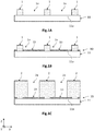
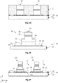
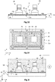
- the Figures 1A to 1K are schematic and partial views, in section, of different steps of a collective manufacturing process of semiconductor structures 20 according to one embodiment.
- the semiconductor structure 20 is a light-emitting diode produced on the basis of InGaN.
- a growth substrate 10 is produced which comprises a support substrate 11 coated at least in part with a nucleation layer 13.
- the support substrate 11 has an upper face 11a intended to receive the nucleation layer 13. It can be made of the same material, and thus be a solid substrate ( bulk substrate, in English), or be formed of a stack of several layers of different materials, such as a SOI type substrate ( Silicon On Insulator, in English).
- the material defining the upper face 11a can be electrically insulating or conductive.
- such an insulating material can be chosen from sapphire (Al 2 O 3 ), borosilicate, silica, glass, quartz, an oxide or a nitride of silicon or aluminum, among others.
- III-V compounds can be III-N compounds, such as GaN, InGaN, AlN, InN or AlInGaN, or compounds comprising an element of column V, for example AsGa or the InP.
- Compounds II-VI can be CdTe, HgTe, CdHgTe, ZnO, ZnMgO, CdZnO or CdZnMgO.
- elements or compounds IV can be Si, C, Ge, SiC, SiGe, GeC, among others.
- the semiconductor material can be doped to increase its electrical conductivity.
- the material of the support substrate 11 defining the upper face 11a can be chosen from metallic materials (Ti, Au, TiAu, etc.) and semi-metallic materials (TiN, etc.).
- the support substrate 11 is here a monobloc substrate made of sapphire.
- a first growth mask 1 is produced on the upper face 11a, intended to subsequently define a free surface of the upper face 11a of the support substrate 11 capable of receiving a working electrode.
- a dielectric layer is deposited on the upper face 11a of the support substrate 11.
- the dielectric layer is made of at least one electrically insulating material, for example a silicon oxide or nitride, such as SiO 2 or Si 3 N 4 , or even a silicon oxynitride, an aluminum oxide, or a hafnium oxide. It may have a dimension along the Z axis, ie a thickness of between a few hundred nanometers and a few microns or tens of microns, for example equal to around 10 ⁇ m.
- the first localized growth mask 1 then forms a mesh of dielectric bands.
- the free surfaces can have, in the XY plane, a circular, oval or polygonal shape, for example square or rectangular. For example, they have a square shape of approximately 100 ⁇ m per side. The dimensions of the free surface depend in particular on those of the semiconductor structures that it is desired to manufacture.
- Each dielectric strip 1 has an initial width, i.e.
- the dielectric strips 1 have an initial thickness equal to approximately 15 ⁇ m and an initial width equal to approximately 15 ⁇ m.
- the initial width of the dielectric strips depends in particular on the dimensions of the working electrode intended to be produced subsequently.
- the nucleation layer 13 is then deposited on the free surfaces of the upper face 11a of the support substrate 11 (fig.iB).
- the nucleation layer 13 can be deposited by epitaxial growth by molecular jets (MBE, for Molecular Beam Epitaxy, in English).
- MBE molecular jets
- Other deposition techniques are possible, for example by chemical vapor deposition (CVD, for Chemical Vapor Deposition, in English) such as chemical deposition with organometallic precursors (MOCVD), or any other suitable deposit technique.
- the nucleation layer 13 is made of tungsten sulfide WS 2 which is particularly suitable for the nucleation of a semiconductor compound based on InGaN.
- the nucleation layer 13 preferably has a number of monolayers chosen such that the separation of the semiconductor structures 20 from the support substrate 11 by electrochemical ablation is carried out before they oxidize, if necessary applicable.
- the semiconductor structures 20 are then produced by van der Waals epitaxy. These are made so as to define a lateral zone 3 which surrounds the semiconductor structures 20 in which are intended to be located a free surface 14 of the nucleation layer 13 and a conductive surface 31 of a working electrode 30.
- the growth mask 2 here has a final thickness greater than the initial thickness of the growth mask 1, the value of the final thickness being a function of the desired dimensions of the semiconductor structures 20.
- a second dielectric layer is deposited so as to completely cover the nucleation layer 13 and the first growth mask 1.
- the second dielectric layer is preferably made of a material identical to that of the first growth mask, and has a thickness substantially equal to the desired final value.
- each dielectric strip 2 has the final thickness and a width final greater than the initial width of the growth mask 1.
- each dielectric strip 2 of the growth mask covers laterally, that is to say transversely to its longitudinal extent, part of the nucleation layer 13 . This part covered is intended to form the free surface 14 of the nucleation layer 13.
- the dielectric strips 2 are intended to subsequently form the lateral zone 3 in which the free surface 14 of the nucleation layer 13 and the conductive surface will be located 31 of the working electrode 30.
- the section of the through openings 2a in the XY plane can have different shapes, for example circular, oval, polygonal, for example square or rectangular.
- the through openings 2a can have lateral dimensions, in the XY plane, of between a few hundred nanometers and a few millimeters, depending on the intended applications.
- the nucleation surface has a square shape with a side of 50 ⁇ m, and the dielectric strips 2 have a final width of approximately 65 ⁇ m.
- the semiconductor structures 20 are then produced in the through openings 2a of the growth mask 2, by epitaxial growth of the van der Waals type from the nucleation surfaces (FIG. ID).
- the semiconductor structures 20 are stacks of semiconductor layers produced on the basis of InGaN and forming a pn junction, intended to form light-emitting diodes.
- the epitaxial growth of the semiconductor structures 20 can be carried out by conventional epitaxy techniques, such as CVD deposition, for example MOCVD, MBE epitaxy, HVPE epitaxy, atomic layer epitaxy (ALE, for Atomic Layer). Epitaxy ) , atomic layer deposition (ALD, for Atomic Layer Deposition ) , or even by evaporation or sputtering .
- CVD deposition for example MOCVD, MBE epitaxy, HVPE epitaxy, atomic layer epitaxy (ALE, for Atomic Layer).
- ALE atomic layer epitaxy
- Epitaxy atomic layer deposition
- ALD atomic layer deposition
- the semiconductor structures 20 are produced based on InGaN by chemical deposition MOCVD.
- each semiconductor structure 20 here comprises, from the nucleation surface, a portion of intrinsic InGaN 21 (not intentionally doped), a first portion 22 doped according to a first type of conductivity, for example of type n, an active area 23 formed of several quantum wells each inserted between two barrier layers, and a second portion 24 doped according to a second type of conductivity opposite to the first type, for example of p type.
- the conductivity types can be reversed.
- Other layers may be provided, for example an electron blocking layer located between the active area and the p-doped portion, and an overdoped portion p intended to facilitate the injection of charge carriers from an electrical contact.
- the semiconductor structures 20 are here produced collectively, that is to say simultaneously, so that the doped portions 22, 24 and the active area 23 of each semiconductor structure 20 advantageously have substantially the same characteristics in terms of dimensions, composition, and doping level.
- the portion 21 of intrinsic InGaN being produced by van der Waals epitaxy from the two-dimensional material of the nucleation layer 13, it has a crystal lattice which is not mechanically constrained by that of the nucleation layer 13, nor by that of the support substrate 11.
- the effective lattice parameter of the material of the portion 21 of intrinsic InGaN is substantially equal to its value in the natural state (unconstrained). This results in a good relaxation of the mechanical stresses of the material of the intrinsic InGaN portion along its entire thickness, thus leading to a low density of structural defects such as dislocations of mesh detuning resulting from a possible plastic relaxation of the stresses. .
- the base material of the semiconductor structure 20 is a ternary or quaternary compound based on GaN, such as InGaN
- a high atomic proportion of aluminum makes it possible to absorb light radiation in the ultraviolet (spectral band between 100nm and 400nm).
- the electrical contacts 25, 26 allowing the injection of the charge carriers into the semiconductor structure 20.
- the lateral flanks of the p-doped portion 24, of the active area 23, and a part of the n-doped portion 22 are etched so as to form a recess receiving a first electrical contact 26.
- lateral flank is meant a surface which laterally delimits, in the XY plane, an element, this surface being able to be oriented in a substantially parallel to the axis Z.
- a second electrical contact 25, for example made of a material transparent to the light radiation emitting from the diode, is deposited on the upper face of the p-doped portion 24.
- the semiconductor structure 20 has an aspect ratio which does not necessarily correspond to the actual aspect ratio.
- the growth mask 2 is not shown.
- the semiconductor structure 20 can have a thickness of the order of a few microns to tens or hundreds of microns, while its lateral dimensions can range up to a few millimeters.
- the growth mask 2 is then removed (fig.iF).
- a plurality of semiconductor structures 20 are obtained which are distinct from each other. They are bordered, i.e. surrounded, by a lateral zone 3 which extends between the lateral flanks facing two adjacent semiconductor structures 20.
- the semiconductor structures 20 cover only part of the nucleation layers 13, so that the latter have a free surface 14 in each lateral zone 3.
- the upper face 11a of the support substrate 11 has a free surface 12 located between two adjacent nucleation layers 13. This free surface 12 is intended to receive a working electrode 30.
- the free surface 14 of each nucleation layer 13 has an upper face 14a opposite the support substrate 11, and a lateral border 14b which defines the periphery of the nucleation layer 13 .
- the working electrode 30 resting on the support substrate 11 is then produced (fig.iG). This is located in the lateral zone 3, and arranged so as to leave free, partially or totally, the free surface 14 of the nucleation layer 13.
- the working electrode 30 thus comprises a conductive surface 31, distinct from the nucleation layer 13 and semiconductor structures 20.
- the working electrode 30 is made of an electrically conductive material.
- the material can be a metal, for example chosen from Au, Pt, TiAu, TiN etc. It can also be the two-dimensional material of the nucleation layer 13 when it is electrically conductive, or even the material of the support substrate 11 defining the upper face 11a when it is electrically conductive.
- the working electrode 30 forms a mesh of conductive strips (FIG. 1H) deposited in contact with the upper face 11a of the support substrate 11 and here at a distance from the nucleation layer 13.
- the thickness and width dimensions of the conductive strips can be between a few hundred nanometers and a few microns.
- the working electrode 30 is electrically connected to a voltage source adapted to impose on it a determined electrical potential.
- the semiconductor structures 20 are bordered, here surrounded, by lateral zones in which are located a conductive surface 31 of the working electrode 30, and a free surface 14 of the nucleation layer 13.
- the free surface 14 is here formed by a part of the upper face 14a and by the lateral flanks 14b (lateral border) of the nucleation layer 13.
- the conductive surface 31 is formed by the upper face and by the lateral flanks of the working electrode 30.
- the structure thus obtained is placed in an aqueous electrolyte bath 50, in which is disposed a second electrode, called reference electrode 40, which has a fixed electrical potential.
- the aqueous electrolyte 50 comes into contact, in the lateral zone 3, of the conductive surface 31 of the working electrode 30, and of the free surface 14 of the nucleation layer 13.
- the aqueous electrolyte 50 is a aqueous solution containing ions. It is chosen so as to have sufficient electrical conductivity. In addition, it is chosen so as to be inert with respect to the material or materials of the semiconductor structures 20, so as not to induce structural degradation.
- the aqueous electrolyte 50 may be acidic and have a pH, for example, of about 2. It can be LiCl 1M with a conductivity equal to 70mS.cm.
- a counter electrode, for example. in platinum can be used (assembly with three electrodes), and the reference electrode 40 can be made of Ag / AgCl or calomel (or any other reference electrode compatible with the electrolyte).
- the semiconductor structures 20 are then separated from the growth substrate 10.
- a potential difference is applied between the working electrode 30 and the reference electrode 40.
- the potential can be applied in continuous mode or in pulsed mode.
- the potential has a value sufficient to generate hydroxyl radicals HO • in the aqueous electrolyte 50, at the interface with the conductive surface 31 of the working electrode 30. This value varies depending on the nature of the electrode and the composition and pH of the electrolyte.
- the hydroxyl radicals correspond to the free radicals HO •, that is to say to the neutral form of the hydroxide ions OH - .
- This formation of hydroxyl radicals can be accompanied by oxidation of the conductive surface 31, as indicated in the article of Avasarala et al. entitled Electrochemical oxidation behavior of titanium nitride based electrocatalysts under PEM fuel cell conditions, Electrochimica Acta, 55 (2010) 9024-9034 , in the case of a TiN electrode under oxidizing conditions at a DC voltage of the order of 1.0V to 1.5V.
- the generation of hydroxyl radicals can be accompanied by the formation of nitrogen N 2 gas capable of inducing a localized separation of the nucleation layer 13, which can then improve the separation of the semiconductor structures 20 from the growth substrate 10.
- the separation is carried out by partial or total degradation of at least one intermediate monolayer 13.2 of the two-dimensional material of the nucleation layer 13, to from the free surface 14, and here from at least its lateral border 14b, by an electrochemical ablation phenomenon similar to that described in the article by Das et al. entitled A Self-Limiting Electro-Ablation Technique for the Top-Down Synthesis of Large-Area Monolayer Flakes of 2D Materials, Sci. Rep. 6, 28195 (2016 ).
- the minimum value of the electric potential imposed on the working electrode 30 to cause the generation of hydroxyl radicals can be predetermined by a method of differential pulse voltammetry (DPV for Differential Pulse Voltammetry, in English).
- the hydroxyl radicals As the fig.1J , due to the strong oxidizing power of the hydroxyl radicals, the latter directly attack the chemical bonds of the two-dimensional material (on the edge of the monolayers) from the free surface 14 of the nucleation layer 13, and here from its lateral edge 14b .
- the hydroxyl radicals are adsorbed by the monolayers of the two-dimensional material, here at from the lateral flank and from the free upper face of the nucleation layer 13, in particular via structural surface defects such as dislocations.
- the adsorption of hydroxyl radicals causes progressive degradation of the interlayer monolayer (s) 13.2, by the formation of a plurality of sheets dissociating from the nucleation layer 13.
- the sheets coming from the intermediate monolayers 13.2 dissociate from the nucleation layer 13 all the more easily as their bonding energy with the other monolayers is lower than that connecting the lower monolayer 13.1 to the support substrate 11, and that connecting the upper monolayer 13.3 to the semiconductor structure 20.
- the binding energy between a lower MOS 2 monolayer and a TiN surface in absolute value, is around 1.25eV, while it is around 0.16eV between monolayers spacers of this two-dimensional MoS 2 material.
- the separation of the semiconductor structures 20 is thus obtained with respect to the support substrate 11.
- the semiconductor structures 20 can then be retrieved in order to finalize the manufacture of a functional optoelectronic system.
- the manufacturing process makes it possible to produce one or more semiconductor structures 20 by van der Waals epitaxy and to separate them from their growth substrate 10.
- the separation step takes advantage of an electrochemical ablation reaction of the nucleation layer 13 in two-dimensional material.
- the semiconductor structures 20 do not undergo mechanical action as in the example of the prior art mentioned above, which makes it possible to preserve their optical and / or electronic properties.
- the upper face 11a of the support substrate 11 can be defined by an electrically conductive material.
- the free surface 12 of the support substrate 11, located in the lateral zone 3, can therefore form the conductive surface 31 of the working electrode 30.
- the latter can thus be the conductive material of the support substrate 11, electrically connected to the voltage source.
- the conductive surface 31 can be defined by the free surface 14 of the nucleation layer 13, in the case where the two-dimensional material is made of an electrically conductive material, such as for example. graphene.
- the nucleation layer 13, in the lateral zone 3, can be distinct from the adjacent nucleation layer 13, but as a variant, the different nucleation layers can form the same continuous nucleation layer 13.
- the various semiconductor structures 20 can, before the separation step, be assembled together to the same secondary substrate (not shown), making it possible in particular to subsequently carry out the steps of structuring and forming the electrical contacts.
- the assembly obtained, formed of the growth substrate 10, the semiconductor structures 20 and the secondary substrate is placed in the aqueous electrolyte 50 and the separation step is carried out as described above.
- a plurality of semiconductor structures 20 are thus obtained, separated from the growth substrate 10, and assembled with the secondary substrate.
- the working electrode 30 is formed of a plurality of conductive strips distinct from each other.
- the polarization of one or more conductive strips adjacent to the identified semiconductor structure 20 makes it possible to separate said semiconductor structure 20 selectively.
- the sum of the voltages applied to the conductive strips adjacent to the chosen semiconductor structure makes it possible to reach the potential necessary for the initiation of the electrochemical ablation reaction (therefore in the vicinity of the chosen structure).
Landscapes
- Led Devices (AREA)
- Recrystallisation Techniques (AREA)
- Liquid Deposition Of Substances Of Which Semiconductor Devices Are Composed (AREA)
- Crystals, And After-Treatments Of Crystals (AREA)
Applications Claiming Priority (1)
| Application Number | Priority Date | Filing Date | Title |
|---|---|---|---|
| FR1856466A FR3083916B1 (fr) | 2018-07-13 | 2018-07-13 | Procede de fabrication d'au moins une structure semiconductrice comportant une etape de separation vis-a-vis du substrat de croissance |
Publications (2)
| Publication Number | Publication Date |
|---|---|
| EP3594997A1 true EP3594997A1 (de) | 2020-01-15 |
| EP3594997B1 EP3594997B1 (de) | 2021-03-24 |
Family
ID=64049351
Family Applications (1)
| Application Number | Title | Priority Date | Filing Date |
|---|---|---|---|
| EP19185598.0A Active EP3594997B1 (de) | 2018-07-13 | 2019-07-10 | Herstellungsverfahren von mindestens einer halbleiterstruktur, umfassend einen abtrennschritt vom wachstumssubstrat |
Country Status (3)
| Country | Link |
|---|---|
| US (1) | US10748762B2 (de) |
| EP (1) | EP3594997B1 (de) |
| FR (1) | FR3083916B1 (de) |
Families Citing this family (3)
| Publication number | Priority date | Publication date | Assignee | Title |
|---|---|---|---|---|
| US20220122837A1 (en) * | 2020-10-21 | 2022-04-21 | University Of South Carolina | Approach for Fabricating N-Polar AlxGa1-xN Devices |
| CN114171373B (zh) * | 2021-12-09 | 2025-06-27 | 苏州晶瓴半导体有限公司 | 一种氮化镓-金刚石异质结晶片及其制备方法 |
| WO2024217820A1 (en) * | 2023-04-19 | 2024-10-24 | Ams-Osram International Gmbh | Method for manufacturing a plurality of semiconductor chips |
Citations (3)
| Publication number | Priority date | Publication date | Assignee | Title |
|---|---|---|---|---|
| US6956246B1 (en) * | 2004-06-03 | 2005-10-18 | Lumileds Lighting U.S., Llc | Resonant cavity III-nitride light emitting devices fabricated by growth substrate removal |
| US20110223749A1 (en) * | 2009-09-14 | 2011-09-15 | Sumitomo Electric Industries, Ltd. | Method of forming nitride semiconductor epitaxial layer and method of manufacturing nitride semiconductor device |
| EP2770545A2 (de) * | 2013-02-22 | 2014-08-27 | LG Electronics, Inc. | Wachstumssubstrat, Nitridhalbleiterbauelement und Herstellungsverfahren dafür |
-
2018
- 2018-07-13 FR FR1856466A patent/FR3083916B1/fr not_active Expired - Fee Related
-
2019
- 2019-07-10 EP EP19185598.0A patent/EP3594997B1/de active Active
- 2019-07-11 US US16/508,503 patent/US10748762B2/en active Active
Patent Citations (3)
| Publication number | Priority date | Publication date | Assignee | Title |
|---|---|---|---|---|
| US6956246B1 (en) * | 2004-06-03 | 2005-10-18 | Lumileds Lighting U.S., Llc | Resonant cavity III-nitride light emitting devices fabricated by growth substrate removal |
| US20110223749A1 (en) * | 2009-09-14 | 2011-09-15 | Sumitomo Electric Industries, Ltd. | Method of forming nitride semiconductor epitaxial layer and method of manufacturing nitride semiconductor device |
| EP2770545A2 (de) * | 2013-02-22 | 2014-08-27 | LG Electronics, Inc. | Wachstumssubstrat, Nitridhalbleiterbauelement und Herstellungsverfahren dafür |
Non-Patent Citations (5)
| Title |
|---|
| DAS ET AL.: "A Self-Limiting Electro-Ablation Technique for the Top-Down Synthesis of Large-Area Monolayer Flakes of 2D Materials", SCI. REP., vol. 6, 2016, pages 28195 |
| D'AVASARALA ET AL.: "Electrochemical oxidation behavior of titanium nitride based electrocatalysts under PEMfuel cell conditions", ELECTROCHIMICA ACTA, vol. 55, 2010, pages 9024 - 9034 |
| JEEHWAN KIM ET AL: "Principle of direct van der Waals epitaxy of single-crystalline films on epitaxial graphene", NATURE COMMUNICATIONS, vol. 5, 1 September 2014 (2014-09-01), GB, pages 4836 - 4836, XP055468472, ISSN: 2041-1723, DOI: 10.1038/ncomms5836 * |
| KIM ET AL.: "Principle of direct van der Waals epitaxy of single-crystalline films on epitaxial graphene", NAT. COMM., vol. 5, 2014, pages 4836, XP055468472, DOI: doi:10.1038/ncomms5836 |
| SAPTARSHI DAS ET AL: "A Self-Limiting Electro-Ablation Technique for the Top-Down Synthesis of Large-Area Monolayer Flakes of 2D Materials", SCIENTIFIC REPORTS, vol. 6, no. 1, 21 June 2016 (2016-06-21), pages 1, XP055563998, DOI: 10.1038/srep28195 * |
Also Published As
| Publication number | Publication date |
|---|---|
| FR3083916A1 (fr) | 2020-01-17 |
| US10748762B2 (en) | 2020-08-18 |
| EP3594997B1 (de) | 2021-03-24 |
| US20200020527A1 (en) | 2020-01-16 |
| FR3083916B1 (fr) | 2020-07-17 |
Similar Documents
| Publication | Publication Date | Title |
|---|---|---|
| EP3782193B1 (de) | Herstellungsverfahren einer optoelektronischen vorrichtung mit diodenmatrix | |
| EP3991215B1 (de) | Optoelektronische vorrichtung mit leuchtdioden des axialen typs und herstellungsverfahren dafür | |
| EP3514841B1 (de) | Optoelektronische vorrichtung und verfahren zu ihrer herstellung | |
| US20090146142A1 (en) | Light-emitting device including nanorod and method of manufacturing the same | |
| EP2997605B1 (de) | Optoelektronische vorrichtung und herstellungsverfahren dafür | |
| EP3840016A1 (de) | Verfahren zur herstellung eines substrats, das eine entspannte ingan-schicht umfasst | |
| FR2969995A1 (fr) | Procede de realisation d'un support comportant des nanostructures en nitrure(s) a phase zinc blende | |
| WO2015052456A1 (fr) | Transistor hemt à base d'heterojonction | |
| EP3090450B1 (de) | Optoelektronische vorrichtung mit halbleiterelementen und deren herstellungsverfahren | |
| EP2834189A1 (de) | Optoelektronische halbleiterstruktur mit nanodrähten und verfahren zur herstellung einer solchen struktur | |
| EP3594997B1 (de) | Herstellungsverfahren von mindestens einer halbleiterstruktur, umfassend einen abtrennschritt vom wachstumssubstrat | |
| EP3503222A1 (de) | Verfahren zur herstellung einer optoelektronischen vorrichtung durch aufbringen einer konvertierungsstruktur auf eine emissionsstruktur | |
| EP3241246B1 (de) | Verfahren zur herstellung von halbleiternanodrähten oder -mikrodrähten mit isolierter basis | |
| FR3068994A1 (fr) | Procede de realisation d'une couche cristalline en un compose iii-n par epitaxie van der waals a partir de graphene | |
| CN105304737B (zh) | 一种可控阵列纳米线太阳能电池及其制备方法 | |
| EP3164881B1 (de) | Optoelektronische vorrichtung mit halbleiterbauelementen und verfahren zur herstellung davon | |
| EP3646391B1 (de) | Optoelektronische vorrichtung und verfahren zur herstellung einer optoelektronischen vorrichtung | |
| EP4000107B1 (de) | Leuchtdiode und herstellungsprozess | |
| EP4020604A1 (de) | Verfahren zur herstellung einer optoelektronischen vorrichtung mit gruppe iii nitrid-basierten mikro-leds | |
| WO2014114730A1 (fr) | Procede de fabrication d'une couche a base de nitrure d'element iii par decollement spontane | |
| EP3973579B1 (de) | Optoelektronische vorrichtung mit leuchtdioden, deren dotierter bereich ein äusseres segment basierend auf aluminium und galiumnitrid enthält | |
| EP4658034A1 (de) | Leuchtdiode und verfahren zu deren herstellung | |
| EP2782145A1 (de) | Verfahren zur Herstellung einer Multiverbindungs-Fotovoltaik-Vorrichtung und so hergestellte Multiverbindungs-Fotovoltaik-Vorrichtung |
Legal Events
| Date | Code | Title | Description |
|---|---|---|---|
| PUAI | Public reference made under article 153(3) epc to a published international application that has entered the european phase |
Free format text: ORIGINAL CODE: 0009012 |
|
| STAA | Information on the status of an ep patent application or granted ep patent |
Free format text: STATUS: REQUEST FOR EXAMINATION WAS MADE |
|
| 17P | Request for examination filed |
Effective date: 20190710 |
|
| AK | Designated contracting states |
Kind code of ref document: A1 Designated state(s): AL AT BE BG CH CY CZ DE DK EE ES FI FR GB GR HR HU IE IS IT LI LT LU LV MC MK MT NL NO PL PT RO RS SE SI SK SM TR |
|
| AX | Request for extension of the european patent |
Extension state: BA ME |
|
| RIC1 | Information provided on ipc code assigned before grant |
Ipc: H01L 33/12 20100101ALN20200903BHEP Ipc: H01L 33/00 20100101ALI20200903BHEP Ipc: H01L 21/78 20060101AFI20200903BHEP |
|
| GRAP | Despatch of communication of intention to grant a patent |
Free format text: ORIGINAL CODE: EPIDOSNIGR1 |
|
| STAA | Information on the status of an ep patent application or granted ep patent |
Free format text: STATUS: GRANT OF PATENT IS INTENDED |
|
| RIC1 | Information provided on ipc code assigned before grant |
Ipc: H01L 33/12 20100101ALN20200929BHEP Ipc: H01L 21/78 20060101AFI20200929BHEP Ipc: H01L 33/00 20100101ALI20200929BHEP |
|
| INTG | Intention to grant announced |
Effective date: 20201030 |
|
| GRAS | Grant fee paid |
Free format text: ORIGINAL CODE: EPIDOSNIGR3 |
|
| GRAA | (expected) grant |
Free format text: ORIGINAL CODE: 0009210 |
|
| STAA | Information on the status of an ep patent application or granted ep patent |
Free format text: STATUS: THE PATENT HAS BEEN GRANTED |
|
| AK | Designated contracting states |
Kind code of ref document: B1 Designated state(s): AL AT BE BG CH CY CZ DE DK EE ES FI FR GB GR HR HU IE IS IT LI LT LU LV MC MK MT NL NO PL PT RO RS SE SI SK SM TR |
|
| REG | Reference to a national code |
Ref country code: GB Ref legal event code: FG4D Free format text: NOT ENGLISH |
|
| REG | Reference to a national code |
Ref country code: CH Ref legal event code: EP |
|
| REG | Reference to a national code |
Ref country code: IE Ref legal event code: FG4D Free format text: LANGUAGE OF EP DOCUMENT: FRENCH |
|
| REG | Reference to a national code |
Ref country code: DE Ref legal event code: R096 Ref document number: 602019003385 Country of ref document: DE Ref country code: AT Ref legal event code: REF Ref document number: 1375352 Country of ref document: AT Kind code of ref document: T Effective date: 20210415 |
|
| REG | Reference to a national code |
Ref country code: LT Ref legal event code: MG9D |
|
| PG25 | Lapsed in a contracting state [announced via postgrant information from national office to epo] |
Ref country code: NO Free format text: LAPSE BECAUSE OF FAILURE TO SUBMIT A TRANSLATION OF THE DESCRIPTION OR TO PAY THE FEE WITHIN THE PRESCRIBED TIME-LIMIT Effective date: 20210624 Ref country code: GR Free format text: LAPSE BECAUSE OF FAILURE TO SUBMIT A TRANSLATION OF THE DESCRIPTION OR TO PAY THE FEE WITHIN THE PRESCRIBED TIME-LIMIT Effective date: 20210625 Ref country code: FI Free format text: LAPSE BECAUSE OF FAILURE TO SUBMIT A TRANSLATION OF THE DESCRIPTION OR TO PAY THE FEE WITHIN THE PRESCRIBED TIME-LIMIT Effective date: 20210324 Ref country code: HR Free format text: LAPSE BECAUSE OF FAILURE TO SUBMIT A TRANSLATION OF THE DESCRIPTION OR TO PAY THE FEE WITHIN THE PRESCRIBED TIME-LIMIT Effective date: 20210324 Ref country code: BG Free format text: LAPSE BECAUSE OF FAILURE TO SUBMIT A TRANSLATION OF THE DESCRIPTION OR TO PAY THE FEE WITHIN THE PRESCRIBED TIME-LIMIT Effective date: 20210624 |
|
| PG25 | Lapsed in a contracting state [announced via postgrant information from national office to epo] |
Ref country code: LV Free format text: LAPSE BECAUSE OF FAILURE TO SUBMIT A TRANSLATION OF THE DESCRIPTION OR TO PAY THE FEE WITHIN THE PRESCRIBED TIME-LIMIT Effective date: 20210324 Ref country code: SE Free format text: LAPSE BECAUSE OF FAILURE TO SUBMIT A TRANSLATION OF THE DESCRIPTION OR TO PAY THE FEE WITHIN THE PRESCRIBED TIME-LIMIT Effective date: 20210324 Ref country code: RS Free format text: LAPSE BECAUSE OF FAILURE TO SUBMIT A TRANSLATION OF THE DESCRIPTION OR TO PAY THE FEE WITHIN THE PRESCRIBED TIME-LIMIT Effective date: 20210324 |
|
| REG | Reference to a national code |
Ref country code: NL Ref legal event code: MP Effective date: 20210324 |
|
| REG | Reference to a national code |
Ref country code: AT Ref legal event code: MK05 Ref document number: 1375352 Country of ref document: AT Kind code of ref document: T Effective date: 20210324 |
|
| PG25 | Lapsed in a contracting state [announced via postgrant information from national office to epo] |
Ref country code: NL Free format text: LAPSE BECAUSE OF FAILURE TO SUBMIT A TRANSLATION OF THE DESCRIPTION OR TO PAY THE FEE WITHIN THE PRESCRIBED TIME-LIMIT Effective date: 20210324 |
|
| PG25 | Lapsed in a contracting state [announced via postgrant information from national office to epo] |
Ref country code: LT Free format text: LAPSE BECAUSE OF FAILURE TO SUBMIT A TRANSLATION OF THE DESCRIPTION OR TO PAY THE FEE WITHIN THE PRESCRIBED TIME-LIMIT Effective date: 20210324 Ref country code: EE Free format text: LAPSE BECAUSE OF FAILURE TO SUBMIT A TRANSLATION OF THE DESCRIPTION OR TO PAY THE FEE WITHIN THE PRESCRIBED TIME-LIMIT Effective date: 20210324 Ref country code: CZ Free format text: LAPSE BECAUSE OF FAILURE TO SUBMIT A TRANSLATION OF THE DESCRIPTION OR TO PAY THE FEE WITHIN THE PRESCRIBED TIME-LIMIT Effective date: 20210324 Ref country code: AT Free format text: LAPSE BECAUSE OF FAILURE TO SUBMIT A TRANSLATION OF THE DESCRIPTION OR TO PAY THE FEE WITHIN THE PRESCRIBED TIME-LIMIT Effective date: 20210324 Ref country code: SM Free format text: LAPSE BECAUSE OF FAILURE TO SUBMIT A TRANSLATION OF THE DESCRIPTION OR TO PAY THE FEE WITHIN THE PRESCRIBED TIME-LIMIT Effective date: 20210324 |
|
| PG25 | Lapsed in a contracting state [announced via postgrant information from national office to epo] |
Ref country code: RO Free format text: LAPSE BECAUSE OF FAILURE TO SUBMIT A TRANSLATION OF THE DESCRIPTION OR TO PAY THE FEE WITHIN THE PRESCRIBED TIME-LIMIT Effective date: 20210324 Ref country code: PT Free format text: LAPSE BECAUSE OF FAILURE TO SUBMIT A TRANSLATION OF THE DESCRIPTION OR TO PAY THE FEE WITHIN THE PRESCRIBED TIME-LIMIT Effective date: 20210726 Ref country code: SK Free format text: LAPSE BECAUSE OF FAILURE TO SUBMIT A TRANSLATION OF THE DESCRIPTION OR TO PAY THE FEE WITHIN THE PRESCRIBED TIME-LIMIT Effective date: 20210324 Ref country code: PL Free format text: LAPSE BECAUSE OF FAILURE TO SUBMIT A TRANSLATION OF THE DESCRIPTION OR TO PAY THE FEE WITHIN THE PRESCRIBED TIME-LIMIT Effective date: 20210324 Ref country code: IS Free format text: LAPSE BECAUSE OF FAILURE TO SUBMIT A TRANSLATION OF THE DESCRIPTION OR TO PAY THE FEE WITHIN THE PRESCRIBED TIME-LIMIT Effective date: 20210724 |
|
| REG | Reference to a national code |
Ref country code: DE Ref legal event code: R097 Ref document number: 602019003385 Country of ref document: DE |
|
| PG25 | Lapsed in a contracting state [announced via postgrant information from national office to epo] |
Ref country code: ES Free format text: LAPSE BECAUSE OF FAILURE TO SUBMIT A TRANSLATION OF THE DESCRIPTION OR TO PAY THE FEE WITHIN THE PRESCRIBED TIME-LIMIT Effective date: 20210324 Ref country code: DK Free format text: LAPSE BECAUSE OF FAILURE TO SUBMIT A TRANSLATION OF THE DESCRIPTION OR TO PAY THE FEE WITHIN THE PRESCRIBED TIME-LIMIT Effective date: 20210324 Ref country code: AL Free format text: LAPSE BECAUSE OF FAILURE TO SUBMIT A TRANSLATION OF THE DESCRIPTION OR TO PAY THE FEE WITHIN THE PRESCRIBED TIME-LIMIT Effective date: 20210324 |
|
| PLBE | No opposition filed within time limit |
Free format text: ORIGINAL CODE: 0009261 |
|
| STAA | Information on the status of an ep patent application or granted ep patent |
Free format text: STATUS: NO OPPOSITION FILED WITHIN TIME LIMIT |
|
| PG25 | Lapsed in a contracting state [announced via postgrant information from national office to epo] |
Ref country code: SI Free format text: LAPSE BECAUSE OF FAILURE TO SUBMIT A TRANSLATION OF THE DESCRIPTION OR TO PAY THE FEE WITHIN THE PRESCRIBED TIME-LIMIT Effective date: 20210324 |
|
| 26N | No opposition filed |
Effective date: 20220104 |
|
| PG25 | Lapsed in a contracting state [announced via postgrant information from national office to epo] |
Ref country code: MC Free format text: LAPSE BECAUSE OF FAILURE TO SUBMIT A TRANSLATION OF THE DESCRIPTION OR TO PAY THE FEE WITHIN THE PRESCRIBED TIME-LIMIT Effective date: 20210324 |
|
| REG | Reference to a national code |
Ref country code: BE Ref legal event code: MM Effective date: 20210731 |
|
| PG25 | Lapsed in a contracting state [announced via postgrant information from national office to epo] |
Ref country code: IS Free format text: LAPSE BECAUSE OF FAILURE TO SUBMIT A TRANSLATION OF THE DESCRIPTION OR TO PAY THE FEE WITHIN THE PRESCRIBED TIME-LIMIT Effective date: 20210724 Ref country code: LU Free format text: LAPSE BECAUSE OF NON-PAYMENT OF DUE FEES Effective date: 20210710 |
|
| PG25 | Lapsed in a contracting state [announced via postgrant information from national office to epo] |
Ref country code: IE Free format text: LAPSE BECAUSE OF NON-PAYMENT OF DUE FEES Effective date: 20210710 Ref country code: BE Free format text: LAPSE BECAUSE OF NON-PAYMENT OF DUE FEES Effective date: 20210731 |
|
| PG25 | Lapsed in a contracting state [announced via postgrant information from national office to epo] |
Ref country code: IT Free format text: LAPSE BECAUSE OF FAILURE TO SUBMIT A TRANSLATION OF THE DESCRIPTION OR TO PAY THE FEE WITHIN THE PRESCRIBED TIME-LIMIT Effective date: 20210324 |
|
| REG | Reference to a national code |
Ref country code: CH Ref legal event code: PL |
|
| PG25 | Lapsed in a contracting state [announced via postgrant information from national office to epo] |
Ref country code: LI Free format text: LAPSE BECAUSE OF NON-PAYMENT OF DUE FEES Effective date: 20220731 Ref country code: CH Free format text: LAPSE BECAUSE OF NON-PAYMENT OF DUE FEES Effective date: 20220731 |
|
| PG25 | Lapsed in a contracting state [announced via postgrant information from national office to epo] |
Ref country code: CY Free format text: LAPSE BECAUSE OF FAILURE TO SUBMIT A TRANSLATION OF THE DESCRIPTION OR TO PAY THE FEE WITHIN THE PRESCRIBED TIME-LIMIT Effective date: 20210324 |
|
| PG25 | Lapsed in a contracting state [announced via postgrant information from national office to epo] |
Ref country code: HU Free format text: LAPSE BECAUSE OF FAILURE TO SUBMIT A TRANSLATION OF THE DESCRIPTION OR TO PAY THE FEE WITHIN THE PRESCRIBED TIME-LIMIT; INVALID AB INITIO Effective date: 20190710 |
|
| PG25 | Lapsed in a contracting state [announced via postgrant information from national office to epo] |
Ref country code: MK Free format text: LAPSE BECAUSE OF FAILURE TO SUBMIT A TRANSLATION OF THE DESCRIPTION OR TO PAY THE FEE WITHIN THE PRESCRIBED TIME-LIMIT Effective date: 20210324 |
|
| PG25 | Lapsed in a contracting state [announced via postgrant information from national office to epo] |
Ref country code: MT Free format text: LAPSE BECAUSE OF FAILURE TO SUBMIT A TRANSLATION OF THE DESCRIPTION OR TO PAY THE FEE WITHIN THE PRESCRIBED TIME-LIMIT Effective date: 20210324 |
|
| PGFP | Annual fee paid to national office [announced via postgrant information from national office to epo] |
Ref country code: DE Payment date: 20250722 Year of fee payment: 7 |
|
| PGFP | Annual fee paid to national office [announced via postgrant information from national office to epo] |
Ref country code: GB Payment date: 20250724 Year of fee payment: 7 |
|
| PGFP | Annual fee paid to national office [announced via postgrant information from national office to epo] |
Ref country code: FR Payment date: 20250722 Year of fee payment: 7 |
|
| REG | Reference to a national code |
Ref country code: DE Ref legal event code: R079 Ref document number: 602019003385 Country of ref document: DE Free format text: PREVIOUS MAIN CLASS: H01L0021780000 Ipc: H10P0058000000 |
|
| PG25 | Lapsed in a contracting state [announced via postgrant information from national office to epo] |
Ref country code: TR Free format text: LAPSE BECAUSE OF FAILURE TO SUBMIT A TRANSLATION OF THE DESCRIPTION OR TO PAY THE FEE WITHIN THE PRESCRIBED TIME-LIMIT Effective date: 20210324 |