EP4020604A1 - Verfahren zur herstellung einer optoelektronischen vorrichtung mit gruppe iii nitrid-basierten mikro-leds - Google Patents
Verfahren zur herstellung einer optoelektronischen vorrichtung mit gruppe iii nitrid-basierten mikro-leds Download PDFInfo
- Publication number
- EP4020604A1 EP4020604A1 EP21216425.5A EP21216425A EP4020604A1 EP 4020604 A1 EP4020604 A1 EP 4020604A1 EP 21216425 A EP21216425 A EP 21216425A EP 4020604 A1 EP4020604 A1 EP 4020604A1
- Authority
- EP
- European Patent Office
- Prior art keywords
- layer
- nitride
- semi
- polar
- facets
- Prior art date
- Legal status (The legal status is an assumption and is not a legal conclusion. Google has not performed a legal analysis and makes no representation as to the accuracy of the status listed.)
- Granted
Links
Images







Classifications
-
- H—ELECTRICITY
- H10—SEMICONDUCTOR DEVICES; ELECTRIC SOLID-STATE DEVICES NOT OTHERWISE PROVIDED FOR
- H10H—INORGANIC LIGHT-EMITTING SEMICONDUCTOR DEVICES HAVING POTENTIAL BARRIERS
- H10H20/00—Individual inorganic light-emitting semiconductor devices having potential barriers, e.g. light-emitting diodes [LED]
- H10H20/01—Manufacture or treatment
- H10H20/011—Manufacture or treatment of bodies, e.g. forming semiconductor layers
- H10H20/013—Manufacture or treatment of bodies, e.g. forming semiconductor layers having light-emitting regions comprising only Group III-V materials
- H10H20/0137—Manufacture or treatment of bodies, e.g. forming semiconductor layers having light-emitting regions comprising only Group III-V materials the light-emitting regions comprising nitride materials
-
- H—ELECTRICITY
- H10—SEMICONDUCTOR DEVICES; ELECTRIC SOLID-STATE DEVICES NOT OTHERWISE PROVIDED FOR
- H10H—INORGANIC LIGHT-EMITTING SEMICONDUCTOR DEVICES HAVING POTENTIAL BARRIERS
- H10H20/00—Individual inorganic light-emitting semiconductor devices having potential barriers, e.g. light-emitting diodes [LED]
- H10H20/01—Manufacture or treatment
- H10H20/011—Manufacture or treatment of bodies, e.g. forming semiconductor layers
- H10H20/013—Manufacture or treatment of bodies, e.g. forming semiconductor layers having light-emitting regions comprising only Group III-V materials
- H10H20/0133—Manufacture or treatment of bodies, e.g. forming semiconductor layers having light-emitting regions comprising only Group III-V materials with a substrate not being Group III-V materials
- H10H20/01335—Manufacture or treatment of bodies, e.g. forming semiconductor layers having light-emitting regions comprising only Group III-V materials with a substrate not being Group III-V materials the light-emitting regions comprising nitride materials
-
- H—ELECTRICITY
- H10—SEMICONDUCTOR DEVICES; ELECTRIC SOLID-STATE DEVICES NOT OTHERWISE PROVIDED FOR
- H10H—INORGANIC LIGHT-EMITTING SEMICONDUCTOR DEVICES HAVING POTENTIAL BARRIERS
- H10H20/00—Individual inorganic light-emitting semiconductor devices having potential barriers, e.g. light-emitting diodes [LED]
- H10H20/01—Manufacture or treatment
- H10H20/011—Manufacture or treatment of bodies, e.g. forming semiconductor layers
- H10H20/018—Bonding of wafers
-
- H—ELECTRICITY
- H10—SEMICONDUCTOR DEVICES; ELECTRIC SOLID-STATE DEVICES NOT OTHERWISE PROVIDED FOR
- H10H—INORGANIC LIGHT-EMITTING SEMICONDUCTOR DEVICES HAVING POTENTIAL BARRIERS
- H10H20/00—Individual inorganic light-emitting semiconductor devices having potential barriers, e.g. light-emitting diodes [LED]
- H10H20/80—Constructional details
- H10H20/81—Bodies
- H10H20/817—Bodies characterised by the crystal structures or orientations, e.g. polycrystalline, amorphous or porous
-
- H—ELECTRICITY
- H10—SEMICONDUCTOR DEVICES; ELECTRIC SOLID-STATE DEVICES NOT OTHERWISE PROVIDED FOR
- H10H—INORGANIC LIGHT-EMITTING SEMICONDUCTOR DEVICES HAVING POTENTIAL BARRIERS
- H10H20/00—Individual inorganic light-emitting semiconductor devices having potential barriers, e.g. light-emitting diodes [LED]
- H10H20/80—Constructional details
- H10H20/81—Bodies
- H10H20/822—Materials of the light-emitting regions
- H10H20/824—Materials of the light-emitting regions comprising only Group III-V materials, e.g. GaP
- H10H20/825—Materials of the light-emitting regions comprising only Group III-V materials, e.g. GaP containing nitrogen, e.g. GaN
-
- H—ELECTRICITY
- H10—SEMICONDUCTOR DEVICES; ELECTRIC SOLID-STATE DEVICES NOT OTHERWISE PROVIDED FOR
- H10H—INORGANIC LIGHT-EMITTING SEMICONDUCTOR DEVICES HAVING POTENTIAL BARRIERS
- H10H20/00—Individual inorganic light-emitting semiconductor devices having potential barriers, e.g. light-emitting diodes [LED]
- H10H20/80—Constructional details
- H10H20/85—Packages
- H10H20/857—Interconnections, e.g. lead-frames, bond wires or solder balls
-
- H—ELECTRICITY
- H10—SEMICONDUCTOR DEVICES; ELECTRIC SOLID-STATE DEVICES NOT OTHERWISE PROVIDED FOR
- H10H—INORGANIC LIGHT-EMITTING SEMICONDUCTOR DEVICES HAVING POTENTIAL BARRIERS
- H10H29/00—Integrated devices, or assemblies of multiple devices, comprising at least one light-emitting semiconductor element covered by group H10H20/00
- H10H29/10—Integrated devices comprising at least one light-emitting semiconductor component covered by group H10H20/00
- H10H29/14—Integrated devices comprising at least one light-emitting semiconductor component covered by group H10H20/00 comprising multiple light-emitting semiconductor components
- H10H29/142—Two-dimensional arrangements, e.g. asymmetric LED layout
-
- H—ELECTRICITY
- H10—SEMICONDUCTOR DEVICES; ELECTRIC SOLID-STATE DEVICES NOT OTHERWISE PROVIDED FOR
- H10H—INORGANIC LIGHT-EMITTING SEMICONDUCTOR DEVICES HAVING POTENTIAL BARRIERS
- H10H20/00—Individual inorganic light-emitting semiconductor devices having potential barriers, e.g. light-emitting diodes [LED]
- H10H20/01—Manufacture or treatment
- H10H20/036—Manufacture or treatment of packages
- H10H20/0364—Manufacture or treatment of packages of interconnections
-
- H—ELECTRICITY
- H10—SEMICONDUCTOR DEVICES; ELECTRIC SOLID-STATE DEVICES NOT OTHERWISE PROVIDED FOR
- H10H—INORGANIC LIGHT-EMITTING SEMICONDUCTOR DEVICES HAVING POTENTIAL BARRIERS
- H10H20/00—Individual inorganic light-emitting semiconductor devices having potential barriers, e.g. light-emitting diodes [LED]
- H10H20/80—Constructional details
- H10H20/81—Bodies
- H10H20/815—Bodies having stress relaxation structures, e.g. buffer layers
-
- H—ELECTRICITY
- H10—SEMICONDUCTOR DEVICES; ELECTRIC SOLID-STATE DEVICES NOT OTHERWISE PROVIDED FOR
- H10W—GENERIC PACKAGES, INTERCONNECTIONS, CONNECTORS OR OTHER CONSTRUCTIONAL DETAILS OF DEVICES COVERED BY CLASS H10
- H10W90/00—Package configurations
Definitions
- the present invention relates to the field of optoelectronic devices comprising LEDs (light-emitting diodes) based on nitride, for example gallium nitride (GaN), as well as an electronic circuit for controlling these LEDs.
- the invention finds a particularly advantageous application in the field of optoelectronic devices in which the LEDs are of micrometric size. These LEDs are then often designated by the expression “micro-LED”.
- a particularly advantageous use of the invention relates to the production of small screens generally called micro-screens or even micro-displays. Another advantageous use relates for example to the production of projectors.
- Nitride-based micro-LEDs in particular based on gallium nitride (GaN), are very interesting for augmented reality applications because they make it possible to manufacture very compact and very bright microdisplays.
- the luminance is around 1 MCd/m 2 which is much higher than what OLED (organic LED) technologies allow, the luminance of which does not exceed a few thousand Cd/m 2 .
- optoelectronic devices comprising LEDs and an electronic circuit making it possible to individually control the LEDs to display images.
- FIG. 1A illustrates a stack 1 comprising a substrate 11 carrying the LEDs 12.
- the control circuit 2 is illustrated in figure 1B . It may comprise a semiconductor substrate 21, for example a silicon substrate.
- the control circuit 21 is produced in CMOS technology.
- the control circuit 2 comprises a plurality of metal pads 22. Each pad 22 is intended to be connected to an electrode of an LED 12, in order to be able to control the LEDs individually.
- the stack 1 comprising the LEDs 12 and the control circuit 2 is coupled by transfer as illustrated in figure 1C thus leading to a hybrid structure.
- This technique therefore includes the transfer of these two structures 1, 2, which imposes strong constraints in terms of alignment of the LEDs 12 and the metal pads 22.
- the substrate support 11 carrying the LEDs 12 can then be removed.
- a drawback of this manufacturing method lies in the need to precisely align the control circuit and the stack comprising the LEDs during the assembly step of these two elements, so that each LED is well positioned. on the corresponding metal stud in the control circuit.
- This alignment is particularly difficult to achieve when the pitch of the pixels decreases, and constitutes an obstacle to increasing the resolution and/or the integration density of the pixels.
- the pitch of the pixels cannot be less than 5 micrometers.
- the proposed method makes it possible to obtain micro-LEDs, of very small size and formed in a semi-polar layer of nitride having few dislocations. This makes it possible to obtain screens whose pitch is very small and whose electro-optical performance is considerably improved.
- the assembly carrying the semi-polar layer of nitride makes it possible to reduce the dislocations in this layer, in particular at the level of the grain boundaries.
- the proposed method has the advantage that, during the step of transferring the nitride layer onto the control circuit, the positions of the various LEDs of the device are not yet defined. There is therefore no strong constraint in terms of alignment precision during the transfer.
- the delimitation of the various LEDs in the active stack can then be carried out by conventional structuring methods which offer an alignment precision markedly higher than the precision which can be obtained when transferring one substrate onto another.
- the proposed method is particularly reliable and inexpensive.
- micro-LEDs of various colors.
- the use of materials in a semi-polar orientation allows more indium to be incorporated into the nitride layer. It is then possible to obtain LEDs emitting in the wavelength from green to red and which offer better quality, in particular in terms of yield than with known solutions. Furthermore, it is possible to obtain LEDs emitting in the red wavelength.
- said facets having a crystal orientation ⁇ 111 ⁇ have a width F132 and the grooves are arranged periodically according to a period P, the ratio P/F132 being such that P/F132 ⁇ 3, preferably, P/F132 ⁇ 5 and preferably P/F132 ⁇ 10.
- the width F132 is measured from a top of the grooves to a bottom of the grooves and in a perpendicular direction to a main direction of extension of the grooves.
- This ratio allows the adhesion of the semi-polar structure to be sufficient to allow controlled execution of the method, in particular during epitaxial growth, while facilitating the separation of this semi-polar structure from its growth substrate.
- F132 is measured along a direction common to the plane of the facets oriented ⁇ 111> and to a plane perpendicular to a main plane in which extends a second face of the semi-polar nitride layer opposite the first face.
- step d) of removing the growth substrate comprises applying a mechanical action to at least one of the growth substrate and the semi-polar nitride structure.
- the application of a mechanical action preferably comprises fracture initiation from an edge of one of the growth substrate and the semi-polar nitride structure using a blunt object.
- the semi-polar nitride layer comprises an alternation of first zones and second zones forming bands or lines parallel to the grooves, the first zones having first dislocation densities D51 and the second zones having second densities D52 dislocations, with D51>K1*D52, with K1>10, preferably K1>100.
- D51 corresponds to a minimum density and D52 corresponds to a maximum density.
- the second zones are distributed periodically in the semi-polar nitride layer, for example on a second face opposite the first face, according to a period P51 and the electrical connection pads are distributed so that the majority and preferably that all the second zones are respectively located in line with a single electrical connection pad.
- the distribution of the first zones is configured so that the first zones are removed by step f) of forming the trenches.
- the LEDs do not include areas of high defect densities.
- the LEDs are formed in the zones having low or zero defect densities. The quality of the optoelectronic device is thereby further improved.
- epitaxy is organometallic vapor phase epitaxy (MOVPE). Nevertheless, other epitaxy techniques can be perfectly envisaged within the scope of the present invention.
- MOVPE organometallic vapor phase epitaxy
- the electrical connection pads are separated from each other by electrically insulating regions, the first areas being located in line with the electrically insulating regions.
- the electrical connection pads are distributed periodically according to a period P220.
- the pitch P220 of the electrical connection pads and the pitch P51 of the second zones are identical. This makes it possible to have a precise connection of each of the LEDs to the pads while reducing the positioning constraints of the assembly on the control circuit.
- step e) of removing the crystallites comprises a chemical mechanical polishing (CMP) step.
- CMP chemical mechanical polishing
- the first face is substantially planar.
- the method further comprises, after step f) of forming the trenches, a step of depositing, on each LED, an electrode on and in contact with the first face of the semi-polar layer of nitride .
- the crystalline layer is a layer based on silicon
- the growth substrate is a semiconductor-on-insulator (SOI) type substrate or a silicon-on-sapphire (SOS) type substrate.
- SOI semiconductor-on-insulator
- SOS silicon-on-sapphire
- the supply of the assembly comprises the supply of the growth substrate and a step of epitaxial growth of the semi-polar nitride structure from said facets having a crystal orientation ⁇ 111 ⁇ .
- the growth substrate comprises a barrier layer on which the crystalline layer rests in direct contact, the barrier layer being configured to allow epitaxial growth of the semi-polar nitride structure from the crystal layer with no epitaxial growth from the stop layer.
- the crystalline layer is based on silicon or is made of silicon and the facets are formed by or are covered by a crystalline buffer layer, the crystalline buffer layer is preferably made of AlN.
- the epitaxial growth step comprises: a first epitaxial growth of a material based on aluminum nitride (AIN) from said facets with ⁇ 111 ⁇ crystal orientation; then at least one second epitaxial growth of a material based on gallium nitride (GaN) from said material based on aluminum nitride (AIN).
- AIN aluminum nitride
- GaN gallium nitride
- the grooves extend along a first direction which corresponds to a direction common to the plane of said upper surface and to the ⁇ 111> plane.
- step e) of removing the crystallites is first carried out and then step f) of forming the trenches is carried out.
- micro-LED designates an LED of which at least one dimension taken in a plane parallel to the main plane in which extends the substrate supporting the micro-LED (i.e., the xy plane of the orthogonal reference referenced in the figures) is micrometric, that is to say strictly less than 1 mm (10-3 meters) and preferably between 0.2 and 100 ⁇ m (10-6 meters).
- the micro-LEDs have, in projection in a main extension plane parallel to the main faces of the micro-LEDs, i.e., parallel to an upper face of the substrate, maximum dimensions of micrometric dimension in the plane .
- these maximum dimensions are less than a few hundred micrometers.
- these maximum dimensions are less than 500 ⁇ m.
- the terms “over”, “overcomes”, “covers” or “underlying” or their equivalents do not mean “in contact with”.
- the deposition of a first layer on a second layer does not necessarily mean that the two layers are directly in contact with one another, but it does mean that the first layer at least partially covers the second layer. by being either directly in contact with it, or by being separated from it by at least one other layer or at least one other element, including air.
- stages of formation of the various layers and regions are understood in the broad sense: they can be carried out in several sub-stages which are not necessarily strictly successive.
- step means the performance of part of the method, and can designate a set of sub-steps.
- stage does not necessarily mean that the actions carried out during a stage are simultaneous or immediately successive. Certain actions of a first step can in particular be followed by actions linked to a different step, and other actions of the first step can be resumed afterwards. Thus, the term step does not necessarily mean unitary and inseparable actions in time and in the sequence of the phases of the process.
- insulator or "dielectric” qualify a material whose electrical conductivity is low enough in the given application to serve as an insulator.
- a dielectric material preferably has a dielectric constant of less than 7.
- the spacers are typically formed from a dielectric material.
- a resin is an organic or organo-mineral material that can be shaped by exposure to a beam of electrons, photons or X-rays or mechanically. Mention may be made, by way of example, of resins conventionally used in microelectronics, resins based on polystyrene (PS), methacrylate (for example polymethyl methacrylate PMMA), Hydrosilsesquioxane (HSQ), polyhydroxystyrene (PHS) etc.
- PS polystyrene
- methacrylate for example polymethyl methacrylate PMMA
- PHSQ polyhydroxystyrene
- PHS polyhydroxystyrene
- optoelectronic device any type of device produced with microelectronic means and comprising at least one optical function. It can also be an intermediate product solely intended for the production of another optoelectronic device.
- a substrate, a layer, a device, "based" on a material M is understood to mean a substrate, a layer, a device comprising this material M only or this material M and possibly other materials, for example elements alloy, impurities or doping elements.
- a "nitride-based layer” can be a layer made only of this nitride or be made of a nitride added with other species or dopants.
- a nitride layer or structure made at least in part of a nitride (N) obtained from at least one of gallium (Ga), indium (In) and aluminum ( Al), can be a layer or a structure based on GaN, InN, AlN, InGaN, AlGaN, AlInN.
- the thickness of a layer or of the substrate is measured in a direction perpendicular to the surface along which this layer or this substrate has its maximum extension.
- the thickness of the horizontal layers is taken along the vertical.
- dopings are non-limiting examples.
- the invention covers all the embodiments in which the dopings are reversed.
- an exemplary embodiment mentions a P doping for a first zone and an N doping for a second zone the present description then describes, implicitly at least, the opposite example in which the first zone has an N doping and the second zone a doping P.
- a doping denoted P+ means that it is a P-type doping (doping by positive charges) and whose content of doping species is greater than or equal to 1 atom of the doping species for less of 1000 atoms of the semiconductor and preferably for less than 10 to 100 atoms of the material forming the semiconductor layer.
- an N+ doping means that it is an N-type doping (doping by negative charges) and whose doping species content is greater than or equal to 1 atom of the doping species for less than 1000 atoms of the semiconductor and preferably for less than 10 to 100 atoms of the material forming the semiconductor layer.
- a doping denoted P encompasses all dopings by carriers of positive charges whatever the content of the doping.
- a P doping comprises the P+ doping contents and the P doping contents lower than the P+ type doping.
- a doping denoted N encompasses all doping by negative charge carriers regardless of the content of the doping.
- an N doping includes the N+ doping contents and the N doping contents lower than the N+ type doping.
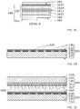
- FIG 2A schematically illustrates an assembly 100 comprising a growth substrate 101 supporting a structure 160 comprising a layer of semi-polar nitride 162.
- figure 2B shows an enlargement of area A of this assembly 100.
- the growth substrate 101 comprises a crystalline layer 130 comprising a plurality of grooves 131 or parallel trenches. They are preferably organized in the form of a network, preferably periodic. Each groove 131 defines at least two opposed inclined facets 132, 133 each forming a band. These bands are continuous or discontinuous in the length direction. At least one 132 of the two opposite facets 132, 133 has a ⁇ 111 ⁇ crystal orientation. Thus, the crystalline layer 130 is chosen so as to present, after etching, facets of ⁇ 111 ⁇ orientation.
- the growth substrate 101 has a semiconductor-on-insulator type structure.
- the crystalline layer 130 overcomes a stop layer 120 (here an insulating layer) supported by a support substrate 110.
- the growth substrate 101 is a silicon on insulator SOI substrate (acronym for "silicon on insulator).
- the growth substrate 101 is of the silicon-on-sapphire (SOS) type.
- the crystalline layer 130 is then a layer based on silicon surmounting a layer of sapphire and separated from the latter by a dielectric layer usually of SiO2.
- the growth substrate 101 can be solid or “bulk” according to English terminology.
- these substrates have the advantage that the crystalline layer 130 has a very small thickness.
- the epitaxial growth takes place from a very restricted surface which reduces the dislocations in the epitaxial layer.
- the performance of the device fabricated from the nitride layer is therefore improved.
- the crystalline layer 130 has an upper face which in this example is covered by a mask 140 having served, during a prior step not shown, for opening the grooves 131 in the crystalline layer 130.
- the mask 140 is for example made by depositing or growing a layer of silicon oxide (SiO2) or silicon nitride (SiN).
- this growth substrate 101 can also comprise a second mask 147 shaped to mask the facets 133 of the crystalline layer 130 which are opposite to the facets 132 having the crystal orientation ⁇ 111 ⁇ .
- the nitride-based structure 160 has crystallites 161 that extend from the crystalline layer 130 and up to the semi-polar layer 162 of nitride.
- these crystallites 161 have grown by epitaxial growth from the facets 132 presenting the crystal orientation ⁇ 111 ⁇ . Adjacent crystallites then coalesce to form the continuous semi-polar nitride layer 162.
- the contact surface between the nitride-based structure 160 and the growth substrate 101 is limited to the contact surface between the crystallites 161 and the facets 132 having the crystal orientation ⁇ 111 ⁇ .
- This contact surface is small compared to the size of the semi-polar layer 162 of nitride and in particular to the surface of its lower face 163 facing the growth substrate 101.
- the surface of the growth substrate 101 which retains the semi-polar layer 162, typically a thumbnail is very weak in front of the surface of this semi-polar layer.
- these facets 132 of small dimensions make it possible to reduce the surface from which the epitaxial growth is initiated and therefore to limit the number of dislocations generated. which propagate to the surface of the epitaxial semi-polar layer 162.
- the lower face 163 is referred to as the first face.
- the first face we also note the presence of a void in the space 168 between the first face 163 of the semi-polar layer 162 of nitride and the growth substrate 101.
- the semi-polar nitride layer 162 is made at least in part of a nitride (N) obtained from at least one of gallium (Ga), indium (In) and aluminum (Al ). According to one example, it is based on gallium nitride (GaN) or is made of GaN.
- Fig. 2C shows an enlargement of zone B of the semi-polar layer 162 of nitride to show there the dopings carried out within this layer in order to form layers of opposite polarity.
- This figure also illustrates stacks of layers forming quantum wells in this example.
- the stack is subsequently referenced 1622-1624. It may include layers other than layers 1622 to 1624. For example, it may include optional buffer layer 1621 and/or optional electrical contact layer 1625 as will be described later.
- the emissive layer 1623 comprises for example or is constituted by a stack of one or more emissive layers each forming a quantum well, for example based on GaN, InN, InGaN, AIGaN, AIN, AlInGaN, GaP, AIGaP, AlInGaP, or of a combination of one or more of these materials.
- the emissive layer 1623 can be a layer of intrinsic gallium nitride, that is to say not intentionally doped, for example with a concentration of residual donors of between 1015 and 1018 atoms/cm3, for example l order of 1017 atoms/cm3.
- the lower face of the emissive layer 1623 is in contact with the upper face of the 1622 layer, and the upper face of the emissive layer 1623 is in contact with the underside of layer 1624.
- the 2D figure schematically illustrates a control circuit 200, preferably it is an integrated circuit.
- the control circuit 200 is formed in and on a semiconductor substrate 210, for example a silicon substrate.
- the control circuit 200 comprises, on the side of its front face 212, for each of the LEDs of the device, a connection pad 220 intended to be electrically connected to the LED, typically to one of the electrodes (anode or cathode) of this last LED, so as to be able to control a current flowing in the LED and/or apply a voltage to the terminals of the LED.
- connection pads 220 are metal pads.
- the control circuit comprises for example, for each LED, connected to a connection pad 220, an elementary control cell comprising one or more transistors, making it possible to control the current flowing in the LED and/or a voltage applied to the terminals of the LEDs.
- the control circuit 200 is for example produced in CMOS technology.
- the connection pads 220 can be laterally surrounded by a region 230 made of a dielectric material, for example silicon oxide, so that the control circuit 200 has a substantially planar front face 212 comprising an alternation of regions electrically conductive and insulating regions.
- the contact on the electrodes of the LEDs (cathodes or anodes) not connected to the connection pads 220 can be made collectively, for example in a peripheral region of the control circuit 200, via one or more contact pads. connection (not visible in the figure) of the control circuit 200.
- the figure 2E illustrates a step during which the assembly 100 comprising the semi-polar layer 162 of nitride is attached to the control circuit 200. More specifically, the upper face 164 of the semi-polar layer 160 nitride, also referred to as the second face, is attached to the front face 212 of the control circuit 200. For this, the assembly 100 can be turned over, then attached to the control circuit 200, so as to bring the second face 164 of the assembly 100 into contact with the front face 212 of the control circuit 200. During this step, the active stack 1622-1624 of the semi-polar layer 160 of nitride is fixed (bonded) to the control circuit 200.
- the fixing of the nitride layer 162 comprising the active stack 1622-1624 on the control circuit 200 can be obtained by direct molecular bonding between the two surfaces brought into contact.
- the fixing of the two surfaces can be carried out by thermocompression, eutectic bonding, or by any another suitable fastening method.
- connection pads 220 provision is made to form on at least one of the faces 164, 212 intended to be in contact, an electrically conductive layer.
- the figure 2F illustrates a step after the postponing step of the figure 2E , during which the growth substrate 101 of the assembly 100 is removed so as to leave on the control circuit 200 the semi-polar structure 160 of nitride comprising the crystallites 161 and the semi-polar layer 162 of nitride.
- the removal of the growth substrate 101 is obtained by exerting a mechanical action.
- an action can be exerted which generates a shear force between the growth substrate 101 and the semi-polar structure 160 of nitride.
- the contact surface between the growth substrate 101 and the semi-polar structure 160 of nitride is small since it is limited to the contact surface between the crystallites 161 and the facets 132 having the ⁇ 111 ⁇ crystal orientation. This separation therefore takes place in a perfectly controlled manner.
- This method therefore offers a particularly effective solution for transferring a semi-polar layer of nitride onto a control circuit in an inexpensive and reproducible manner.
- the fracture can be initiated by one of the edges of the plate forming the assembly 100, for example using a blunt tool.
- Many processes can be used to initiate or complete this invoice.
- the figure 2G illustrates the stack obtained at the end of the step of removing the growth substrate 101.
- the figure 2H illustrates the result obtained after a crystallite removal step 161.
- This step leaves the semi-polar layer 162 of nitride in place.
- this step comprises planarization, for example by chemical mechanical polishing (CMP).
- CMP chemical mechanical polishing
- the removal of the crystallites 161 can also be carried out chemically.
- the Figure 2I illustrates a step of forming trenches 170 inside the semi-polar layer 162 of nitride to delimit islands 165 or mesas each forming or intended to form a micro-LED.
- the reference 165 will be used both to designate an LED and to designate an island forming or intended to form an LED.
- the trenches form two networks which intersect, preferably at 90°, to define the islands.
- an island is defined between four parallel trenches two by two.
- Each LED or island formed in the stack 1622-1624 is laterally surrounded by a trench 170.
- These trenches 170 are for example formed by etching from the second face 164 of the semi-polar layer 162 of nitride.
- These islands 165 are for example formed by lithography and etching, which offers, with conventional microelectronics techniques, positioning precision very high.
- the assembly 100 and the control circuit 200 can be respectively formed on plates of large dimensions. These plates can example have a diameter or a diagonal of 200 or even 300 millimeters. They present the classic sizes of the plates (wafer) usually used for CMOS technologies.
- the semi-polar layers of nitride used to form the LEDs have much lower performances (in terms of luminescence radiative efficiency for example) in the blue wavelength range. In the green wavelength range this performance is usually much lower. In the red wavelength range, the conventional methods do not make it possible to achieve acceptable performance.
- the semi-polar layer of nitride forming the micro LED of the optoelectronic device obtained with the method according to the invention has very few defects, in particular few dislocations at the level of the coalescence joints between crystallites. These coalescence joints correspond to zones 51 referenced in the Figure 7A which will be described in detail later.
- the method presented above has the advantage of making it possible to obtain micro LEDs of very small size and formed from a semi-polar layer of nitride having a very high quality.
- the screen obtained can thus have a very small pixel pitch.
- micro-LEDs can emit in the red and green wavelengths with improved quality.
- the figures 3A to 3F illustrate a more detailed example of a process for producing optoelectronic devices from the assembly of the control circuit 200 and the semi-polar layer 162 of nitride.
- the first step of this process consists in providing an assembly illustrated in figure 2H and comprising the semi-polar layer 162 of nitride transferred onto the control circuit 200.
- this front face being typically formed by the face of the metallic layer 240: the metallic layer 1625, the layer 1624 of nitride doped with a first doping (typically a P-type doping), the emissive layer 1623 comprising the multiple quantum wells, the layer 1622 of nitride doped with a second doping (typically N-type doping).
- a first doping typically a P-type doping
- the emissive layer 1623 comprising the multiple quantum wells
- the layer 1622 of nitride doped with a second doping typically N-type doping
- the stack 1622-1624 does not illustrate the buffer layer 1621 of nitride.
- This buffer layer 1621 may indeed have been removed during the removal of the crystallites 161 or during a step subsequent to this removal.
- it can be plasma etched. The stopping of this etching can be triggered for the detection of the exposure of the layer 1622 (N-doped for example).
- the Figure 3B illustrates the step of etching the trenches 170 in the active stack 1622-1624, from its upper face 166, for example by lithography then etching, so as to delimit the plurality of LEDs 165.
- Each LED 165 corresponds to an island formed in the stack 162 and laterally surrounded by a trench 170.
- the island may have a circular perimeter or any other shape, for example polygonal (square or rectangle for example).
- the trenches 170 extend vertically over the entire height of the stack 162.
- each LED 165 comprises a vertical stack comprising, in order from the upper face of the metal layer 1625, a portion of the layer of nitride 1624, corresponding to the anode of the LED in this example, a portion of the emissive layer 1623, and a portion of the nitride layer 1622, corresponding to the cathode of the LED in this example.
- the trenches 170 can be aligned with marks previously formed on the control circuit 200.
- each LED 165 is located, in vertical projection, facing a single connection pad 220 of the control circuit 200.
- the trenches 170 are located, in vertical projection, opposite the insulating regions 230 of the upper face of the control circuit 200.
- the metal layer 240 serves as an etching stop layer during the making of the trenches 170 in the active pile 1622-1624.
- the Fig. 3C illustrates a subsequent step of removing, for example by etching, portions of the metal layers 1625 and 240 located at the bottom of the trenches 170, so as to extend the trenches 170 to the insulating regions 230 of the upper face of the control circuit 200.
- the anodes (regions 1625) of the different LEDs 165 are electrically isolated from each other by the trenches 170, and each LED 165 has its anode connected to the underlying metal pad 220 via the portions of metal layers 1625 and 240 remaining between the LED and the pad 220. This allows individual control of the LEDs by the control circuit 200.
- the 3d figure illustrates a subsequent step of depositing, on the flanks of the LEDs 165, an insulating passivation layer 174, for example of silicon oxide.
- the layer 174 is for example deposited on the entire upper surface of the assembly by a conformal deposition technique, then removed only on the upper face of the LEDs 165 and at the bottom of the trenches 170, for example by anisotropic etching.
- the Figure 3E illustrates a stage after the stage of the 3d figure , during which the trenches 170 are filled with an insulating material 176, for example silicon oxide.
- an insulating material 176 for example silicon oxide.
- a layer of silicon oxide thick enough to fill the trenches 170 is deposited over the entire upper surface of the assembly, then a planarization step, for example chemical mechanical polishing (CMP), is carried out. works to remove the silicon oxide on the upper surface of the LEDs 165.
- CMP chemical mechanical polishing
- the upper face 166 of the device is substantially planar and comprises an alternation of insulating regions 174, 176 and nitride regions 1622.
- the step of filling the trenches 170 ( Figure 3E ) and the LED edge passivation step ( 3d figure ) can be combined.
- the Figure 3E also illustrates a step subsequent to the filling of the trenches 170 with the insulating material 176, during which one or more metallizations 178 are formed on the upper face 166 of the device, in contact with the cathode regions 1622 of the LEDs 165.
- the cathode regions of the LEDs 165 are all connected to the same metallization 178.
- the metallization 178 comes into contact, on each of the LEDs 165, with a peripheral part of the upper face of the cathode region 1622 of the LED.
- a central part of the LED is on the other hand not covered by the metal grid 178, so as to allow the passage of the light emitted by the LED.
- the display device is intended to be observed from the side of its upper face 166.
- the metal grid 178 can be connected to the control circuit 200, for example via one or several vias (not shown) formed in the active stack 1622-1624 or in the insulating material 176 filling the trenches 170, for example in a peripheral region of the device.
- the figure 3F illustrates a step subsequent to the deposition of the metallizations 178, during which an insulating layer 180, for example of silicon oxide, is deposited over substantially the entire upper surface of the device, to protect the metallizations 178 and the visible portions of the gallium nitride layer 162.
- the insulating layer 180 can be planarized so as to obtain a display device having a substantially planar upper surface.
- the deposition of the metallic layers 1625 and 240 on the control circuit 200 and on the active stack 1622-1624 prior to the transfer of the active stack 1622-1624 onto the control circuit 200 has several advantages.
- layers 1625 and 240 make it possible to improve the quality of bonding between the two structures. Indeed, although possible, the direct gluing of the upper face (in the orientation of the Figure 1A ) of the nitride layer 1624 on the front surface 212 of the control circuit 200 (comprising an alternation of insulating regions 230 and metallic regions 220) is relatively difficult to achieve.
- layer 1625 can advantageously be chosen to achieve good ohmic contact with nitride layer 1624.
- the material of metal pads 220 of control circuit 200 for example copper or aluminum, may not be suitable for making such an ohmic contact.
- the layers 240 and/or 1625 can comprise a reflective metal for the light emitted by the LEDs 165, so as to increase the emission efficiency and avoid losses of light in the control circuit 200.
- the layer 240 and/or the layer 1625 can be chosen so as to prevent the metal of the connection pads 220 of the control circuit 200, for example copper, from diffusing towards the gallium nitride layer 1624, this which could in particular degrade the quality of the ohmic contact with the layer of gallium nitride 1624.
- each of the layers 240 and 1625 can be a single layer or a stack of one or more layers of different metals making it possible to perform all or part of the aforementioned functions.
- layer 240 comprises an upper layer of a metal of the same nature as upper layer 1625, this metal being chosen to obtain good bonding between the two structures during the stage of the transfer figure illustrated in figure 2E , for example a metal from the group comprising Ti, Ni, Pt, Sn, Au, Ag, Al, Pd, W, Pb, Cu, AuSn, TiSn , NiSn or an alloy of all or part of these materials.
- the stack formed by the layers 240 and 1625 may further comprise one or more layers made of metals suitable for reflecting the light emitted by the LEDs, for example money.
- the stack formed by the layers 240 and 1625 may comprise one or more layers adapted to form a barrier to the diffusion of metals such as copper or silver included in the stack 240/1625 and/or in the pads metal 220, for example layers of TaN, TiN, WN, TiW, or a combination of all or part of these materials.
- the layer 240 and/or the layer 1625 can however be absent.
- at least one of the layers 240 and 1625 is provided, preferably the layer 1625 formed on the side of the active stack 1622-1624 of LEDs.
- This assembly 100 comprises the growth substrate 101 surmounted by a semi-polar structure 160 of nitride.
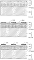
- One step, shown in figure 4A comprises the provision of a stack comprising successively from a support substrate 110: a stop layer 120, a crystalline layer 130, a first masking layer 140 and a second masking layer 145.
- support substrate 110 is silicon.
- Stop layer 120 is an SiO2 layer and crystal layer 130 is a silicon layer.
- the stack 110, 120, 130 preferably forms an elaborate substrate of the silicon-on-insulator (SOI) type, in which the layer 130 constitutes the layer usually designated top Si. As already indicated above, this stack can also be of the type silicon on sapphire, wherein the crystalline layer 130 is a layer of silicon.
- SOI silicon-on-insulator
- the orientation of the superficial crystalline layer 130 of the substrate typically made of silicon, presents a shift in orientation of the crystalline plane (001) of 7° towards [110] so as to then obtain an epitaxial layer of GaN with an orientation (10 -11)
- the first masking layer 140 is a hard mask, for example made of SiO2 or silicon nitride (SiN). This hard mask 140 has for example a thickness of 50 nanometers. This hard mask 140 is covered with a second masking layer 145 typically made or based on resin.
- grooves 131 are then etched in the crystalline layer 130. These grooves 131 are recessed patterns, and thus form trenches.
- parallel strips 141 are produced in the masking layer 140.
- This structuring of the masking layer 140 is carried out in a conventional manner by lithography and etching through the layer 145 forming a resin mask.
- the step of structuring the resin mask 145 and the step of etching the masking layer 140 to form the hard mask are illustrated in figure 4B and 4C .
- the hard mask thus forms parallel bands 141 covering the crystalline layer 130 and leaving exposed other parallel bands of this crystalline layer 130.
- the parallel strips 141 are oriented in a predetermined crystalline direction of the crystalline layer 130.
- the crystalline layer 130 has an internal face facing an upper face 121 of the stop layer 120 and an external face opposite the internal face, said outer face also being referred to as the upper surface.
- the direction of orientation of the parallel strips 141 must correspond to a direction common to the plane of the external face of the crystalline layer 130 and to the plane ⁇ 111> which it is desired to reveal by chemical etching. This direction is a ⁇ 110> type direction.
- the bands 141 are parallel to the intersection between the plane of the upper surface of the crystalline layer 130 and the plane ⁇ 111>.
- the crystalline layer 130 is then chemically etched, using for example KOH (potassium hydroxide) or even tetra-methyl ammonium hydroxide (TMAH).
- KOH potassium hydroxide
- TMAH tetra-methyl ammonium hydroxide
- the grooves 131 thus formed by etching are parallel to the strips 141.
- These grooves 131 define parallel grooves oriented along the direction common to the plane of the external face of the crystalline layer 130 and to the ⁇ 111> plane.
- the etching stops automatically when the stop layer 120 is reached.
- the fact of precisely controlling the depth of the grooves 131 and of obtaining thin trenches makes it possible to greatly reduce the surface from which the crystallites 161 will form. This greatly reduces the number of generated dislocations that propagate to the surface of the semi-polar layer.
- the semi-polar layer 162 formed after coalescence of the crystallites then has a greatly reduced number of dislocations.
- the LEDs formed in this layer then exhibit significantly improved performance.
- melt-back etching takes place randomly on the surface of the crystalline layer 130, a reduction in the surface of the facets 132 makes it possible to considerably reduce or even eliminate the risk of this phenomenon appearing. It will be recalled that the melt-back phenomenon comes from the strong reactivity between the silicon and the GaN and leads to untimely etching of the silicon by the gallium.
- the height e130 of the facet 132 depends on the depth of the groove 131. Facet height 132 and depth of the groove 131 are measured perpendicular to the plane in which the different layers 110, 120, 130 mainly extend i.e. according to the vertical on the figures 4A to 4G .
- the grooves 131 therefore preferably have a flat bottom 121 . This bottom is formed by the upper face 121 of the barrier layer 120.
- the results in terms of reduction of the melt-back etching phenomenon are particularly significant.
- the method makes it possible to obtain semi-polar layers 162 of flat nitride and of more uniform thickness.
- the present invention also applies in the case where the crystalline layer does not overcome a stop layer 120 and forms for example a massive substrate.
- the crystalline layer 130 is made of silicon and the layer of nitride which it is desired to grow by epitaxy is GaN
- This buffer layer 146 can be deposited on the entire upper surface of the growth substrate 101, as illustrated in Figure 4E .
- the facets 132 are formed by or are covered by the buffer layer 146.
- a mask 147 is then formed, configured to cover the entire upper face of the growth substrate 101 with the exception of the orientation facets 132 ⁇ 111 ⁇ . This mask 147 is illustrated on the Figure 4E .
- this masking step is carried out in such a way that the facets 133 of ⁇ 111 ⁇ orientation opposite the facets 132 having a crystalline ⁇ 111 ⁇ orientation are masked.
- the production of this mask 147 typically comprises the deposition of a material comprising at least one of: silicon oxide (SiO2), silicon nitride (SiN), titanium nitride (TiN).
- the deposition of this mask 147 is an angular deposition carried out so that the entire upper surface of the crystalline substrate 130 is masked, with the exception of said facets 132 which have a ⁇ 111 ⁇ crystal orientation.
- the angle of inclination of the deposit means that a part of the groove 131, corresponding to the facets 132, is not exposed and therefore does not therefore receive the deposited material.
- This step is accomplished with the aid of standard equipment known as an ion beam sputter (IBS) in which the deposition angle can be adjusted.
- IBS ion beam sputter
- This deposit with an inclined angle can also be obtained by the technique known as "Electron beam physical vapor deposition” (EBPVD), meaning in French physical deposition in the gas phase by electron beam, in which a vacuum target anode is bombarded by an electron beam.
- EBPVD Electron beam physical vapor deposition
- the crystallites 161 which are then grown from these facets 132 of ⁇ 111 ⁇ orientation are then all of a substantially equal size, except for the uncertainty on the thickness variation e130 of the crystalline layer 130 , greatly facilitating coalescence and obtaining flat semi-polar surfaces 162 over the entire extent of a substrate as illustrated in the figure 4G .
- AlN layer 146 is grown by epitaxy and directly in contact with facets 132 of ⁇ 111 ⁇ orientation of crystalline layer 130. Then, from layer 146, nitride layer 162 is grown by example of GaN.
- the dimensions of the facets 132 of ⁇ 111 ⁇ orientation obtained from the crystalline layer 130 are preferably within a range of values ranging from 20 nm to 2 ⁇ m which corresponds to a range of thicknesses e130 of the crystalline layer 130 of l order of 10 nm to 1 ⁇ m depending on the crystalline orientation of the starting surface.
- the repetition periods of the bands 131 of the mask 140 are preferably included in a range of values ranging from 2 to 10 ⁇ m.
- an additional step is carried out after the step of obtaining the plurality of parallel grooves and before the step of epitaxial growth of the crystalline layer.
- This additional step includes making a plurality of parallel trenches that extend in a direction that has been rotated relative to the main direction in which the parallel grooves 360 extend.
- the grooves 131 are discontinuous.
- the trenches are turned, relative to the grooves 131, by an angle which is greater than 40° and which is preferably between 50° and 90°, this angle is measured in a plane parallel to the plane main in which extends the support substrate 110.
- the trenches thus interrupt the continuous grooves 131 so as to form a matrix of individual facets each having a crystal orientation ⁇ 111 ⁇ .
- the material then grows only from said individual facets which have a crystal orientation ⁇ 111 ⁇ and which form said matrix.
- the trenches and the grooves 131 each having a bottom, the bottom of the trenches being at the same depth or below the bottom of the grooves 131.
- the formation of the trenches, inclined with respect to the grooves 131, makes it possible to reduce the available surface areas of facets exhibiting a ⁇ 111 ⁇ crystal orientation.
- This optional but advantageous embodiment thus allows an even greater reduction in the footprint used for epitaxial growth and thus a reduction in defects during epitaxial growth generated at the GaN/AlN/Si or AlN/Si interface while imposing growth in the proper +c direction.
- Masking layer 140 is made of SiO2. It has a thickness of 50 nanometers. It is deposited directly in contact with the crystalline layer 130. It is produced by ion beam sputtering (IBS).
- the crystalline layer 130 is made of crystalline silicon. It has a thickness of 150 nanometers.
- the stop layer 120 is a layer of SiO2. It has a thickness of 500 nanometers.
- Support substrate 110 is made of silicon.
- the bands 141 are located along the [110] direction. They are defined by standard photolithography with a period of 5 ⁇ m. For example the strips 141 have a width of 2.5 micrometers and the openings between the strips 141 also have a width of 2.5 micrometers.
- the mask 140 made here in SiO2, is etched using an inductively coupled plasma (ICP).
- ICP inductively coupled plasma
- the sample is then cleaned for 30 seconds in a buffered etching oxide (BOE) solution to remove native oxide, an oxide that often prevents KOH from attacking silicon.
- BOE buffered etching oxide
- the substrate is then exposed to wet etching using KOH, revealing the opposing 132 (111) and 133 (11 1) facets.
- these facets 132, 133 have an inclination of 48° and 60°, respectively, with respect to the top surface of Si (6° off (001) top Si).
- the etching would have stopped automatically once a V-shaped groove was fully formed.
- a buffer layer 146 of AlN 50 nm thick is deposited by epitaxy, at 1210° C. by MOVPE (organometallic vapor phase epitaxy).
- MOVPE organometallic vapor phase epitaxy
- the second mask 147 is an SiO2 mask. It is deposited using equipment of the IBS type and with an angle of inclination which makes it possible to leave exposed the facets 132 inclined at 60° in AIN, that is to say where the growth of GaN must be initiated.
- the same MOVPE reactor as that used previously for the deposition of the buffer layer 146 of AlN is used for the selective growth of the semi-polar layer 162 of GaN.
- the precursors are trimethylgallium (TMGa) and ammonia (NH3).
- the growth process can be divided into two stages.
- a first step comprises the growth of crystallites 161 or GaN pyramids. This step is carried out for example at a temperature of 1090° C.
- the pressure can be of the order of 300 Torr.
- the ratio V / III of the flow rate of the gases injected into the reactor can be 1500.
- a second step aims to achieve the coalescence of crystallites 161.
- the growth continues at the same temperature but with a lower pressure (100 Torr) and with a lower V / III ratio (650).
- this process makes it possible to obtain a semi-polar layer. This makes it possible to greatly reduce the effects of polarization, in particular the quantum confined Stark effect in the quantum wells of LED heterostructures, associated with the semi-polar material.
- the epitaxy of quantum well heterostructures on bulk structured silicon and on structured SOI makes it possible to grow layers free of constraints or subjected to little constraint during coalescence.
- the epitaxy of heterostructures with quantum wells makes it possible to generate fewer dislocations which allows better radiative efficiency of the micro-LEDs.
- the layers obtained indeed have average dislocation densities ranging from a few 10E6 (for so-called Aspect Ratio Trapping growth techniques) to a few 10E7 (on standard SOI).
- the figures 5A and 5B are cathodoluminescence images of a GaN layer in which each black point corresponds to an emerging dislocation. The dislocations are confined along zones 51 forming lines corresponding to the coalescence zones of the bands. Zones 51 thus correspond to the coalescence joints. Zones 52 between these lines of dislocations have very low dislocation densities.
- micro-LEDs in these areas 52 with low or even zero defects is an important advantage which can be exploited to increase their radiative efficiency, in particular for long wavelengths.
- An example of judicious exploitation of these zones 52 with a very low defect density will be described in detail later with reference to the figures 7A and 7B .
- the epitaxy of heterostructures with quantum wells makes it possible to have a contact or adhesion surface between the epitaxial semi-polar structure 160 and the weaker growth substrate 101 .
- This contact surface is even smaller when the growth substrate 101 comprises a stop layer 120 limiting the depth of the grooves 131 and therefore the surface of the growth facets 132. It is then possible to adjust the conditions so that the adherence of the semi-polar structure 160 is sufficient to allow an execution control of the process, in particular during epitaxial growth, while facilitating the separation of this semi-polar structure 160 with respect to its growth substrate 101.
- the detachment is for example possible to provide for the detachment to be triggered solely by annealing. Alternatively, provision can be made for this detachment to be favored by the annealing. Provision can be made for this detachment to be entirely carried out in part and preferably entirely by the application of a mechanical stress or by ultrasound as has been described with reference to the figure 2F .
- FIGS. 5C and 5D are scanning electron microscope images of a section of an assembly comprising an epitaxial semi-polar structure 160 resting on its growth substrate 101.
- areas 51 and 52 are referenced.
- Regions 53, 54, 55 are also referenced. These regions 53, 54, 55 come into play in the adhesion of the semi-polar structure 160 to its growth substrate 101.
- the region 53 corresponds to the surface of the facets 132 from which the epitaxy is initiated.
- Region 54 corresponds to an "empty" space which does not allow retention of the semi-polar structure 160 on its growth substrate 101.
- Region 55 corresponds to the surface of the interface between the semi-polar structure 160 and the upper face 121 of stop layer 120, typically a layer of SiO2. This interface participates very little or does not participate in the adhesion of the semi-polar structure 160 to its growth substrate 101. It appears that the surface of the region 53 is very small compared to the other regions 54, 55.
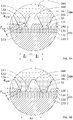
- the figures 6A and 6B schematically illustrate the interface between the semi-polar structure 160 and a growth substrate 101 of the SOI type. These figures make it possible to highlight the parameters which influence the adhesion between the semi-polar structure 160 and its growth substrate 101, and consequently the force which must be applied to detach these two sets 160, 101.
- the ratio P1/F132, respectively P2/F132 contributes significantly to the control of the retention of the semi-polar structure 160 with respect to its growth substrate 101.
- the higher this ratio the lower the retention and the growth substrate 101 can then be detached easily.
- the epitaxy pressure is less than 300 Torrs.
- epitaxy is equal to 100 Torrs.
- this ratio is less than or equal to 2000. Preferably it is less than 1000, advantageously of the order of 650.
- the epitaxy temperature is greater than 1050°C, and preferably the epitaxy is greater than 1100°C.
- a higher temperature makes it possible to increase the mobility of the Ga atoms deposited on the surface, avoiding in particular their accumulation on the upper face 121 of the stop layer 120, which otherwise could cause the layer 160 to adhere to the layer of stop 120 and therefore make its subsequent detachment more difficult.
- the parameter relating to the roughness of the stop layer 120 is also preferable to consider the parameter relating to the roughness of the stop layer 120.
- a smooth, slightly rough material will be preferred in order to limit the deposit on this surface and thus limit the adhesion of the layer.
- epitaxied on this stop layer 120 Preferably, a material allowing selective growth which has a slightly rough surface state such as an oxide will thus be chosen for the stop layer 120.
- SiO2 is a good candidate.
- the stop layer is that which makes up the SOI, therefore most often a layer of SiO2. Its roughness is then that of the Si/SiO2 thermal or Si/SiO2 interface deposited.
- This width "I1” is referenced in Figure 6A ) of the etched zone between two mesa formed by the crystalline layer 130 bearing the facets 132.
- This width I1 must be large enough relative to the width I2 of the mesa (this width “I2” is referenced in Figure 6A ).
- the ratio e I2/I1 ⁇ 20%, preferably e ⁇ 10%.
- Shading effects can also be used to avoid the growth of the semi-polar facet 132 under the pyramid.
- MBE Molecular Beam Epitaxy
- MOVPE Metal Organic Chemical Vapor Deposition
- the defects which occur during epitaxial growth are concentrated in narrow zones 51.
- large areas 52 are defect-free or have a very low defect rate.
- These zones 51 and 52, illustrated in the photos of the figures 5A and 5B are also schematically illustrated in Figure 7A .
- the defect concentration zones 51 are periodically distributed in the semi-polar nitride layer. This period P51 is closely linked to the width of the bands 141 of the hard mask 140 and the width of the grooves 131 etched in the crystalline layer 130 of the growth substrate 101.
- control circuit 200 is configured so that the electrical connection pads 220 are a function of this period P51, so that the majority and preferably all of the zones 52 with a low fault content are located in line with a single electrical connection pad 220. Thus the same zone 52 with low contents is not in contact with two pads 220 of electrical connection.
- the period of the crystallites 161 and therefore the period of the defect concentration zones 51 and the distribution of the electrical connection pads 220 are adapted to achieve this.
- the electrical connection pads 220, at least some of them and preferably all of the pads 220, are periodically distributed over the control circuit 200, according to a period P220.
- P51 X*P220, with X between 0.8 and 1.2, preferably X is between 0.9 and 1.1, preferably X is between 0.95 and 1, 05.
- the period P51 preferably comprises the width of a zone 51 added to the width of a zone 52.
- P51 represents both the distribution period of the zones 51 and of the zones 52.
- the widths of these zones 51, 52 are preferably measured along a direction parallel to the plane of the first and second faces 163, 164 of the epitaxial layer and perpendicular to the main direction of extension of the grooves 131 or strips 141.
- the zones 51 of high concentration of dislocations are located in line with the regions 230 of insulating material 230 separating the adjacent pads 220. More generally, the semi-polar structure 160 and the step of opening the trenches 170 serving to isolate each LED 165 are configured so that the zones 51 are located directly above the trenches 170. Thus, when the step of opening the trenches 170, the zones 51 with a high defect density are eliminated. The LEDs 165 are for their part formed in the zones 52 having low or zero defect densities. The quality of the optoelectronic device is thereby further improved. To implement this embodiment, the distribution, location and size of the areas 51, 52 and of the electrical connection pads 220 will be adapted.
- the zones 51 have mean dislocation densities D51 greater than at least K1 times the mean dislocation densities D52 of the zones 52, with K1>to 10 and preferably K1>to 100.
- the zones 51 substantially perpendicular to the main faces of the semi-polar layer 162 of nitride.
- D51 corresponds to a minimum density observed for these areas 51 in layer 162 and D52 corresponds to a maximum density observed for these areas 52 in this same layer 162.
- D51 corresponds to an average density observed for these areas 51 in layer 162 and D52 corresponds to an average density observed for these zones 52 in this same layer 162.
- positioning marks carried by the control circuit 200 are taken as a reference.
- the proposed method proves to be particularly interesting in the field of microscreens, for example for augmented reality or reality applications. mixed, in the field of ultra high definition (UHD), or even in the field of projectors.
- UHD ultra high definition
Landscapes
- Led Devices (AREA)
Applications Claiming Priority (1)
| Application Number | Priority Date | Filing Date | Title |
|---|---|---|---|
| FR2013978A FR3118306B1 (fr) | 2020-12-22 | 2020-12-22 | Procédé de réalisation d’un dispositif optoélectronique comportant des LED à base de nitrure |
Publications (2)
| Publication Number | Publication Date |
|---|---|
| EP4020604A1 true EP4020604A1 (de) | 2022-06-29 |
| EP4020604B1 EP4020604B1 (de) | 2023-08-30 |
Family
ID=74592262
Family Applications (1)
| Application Number | Title | Priority Date | Filing Date |
|---|---|---|---|
| EP21216425.5A Active EP4020604B1 (de) | 2020-12-22 | 2021-12-21 | Verfahren zur herstellung einer optoelektronischen vorrichtung umfassend gruppe iii nitrid-basierten mikro-leuchtdioden |
Country Status (4)
| Country | Link |
|---|---|
| US (1) | US12080824B2 (de) |
| EP (1) | EP4020604B1 (de) |
| CN (1) | CN114664981A (de) |
| FR (1) | FR3118306B1 (de) |
Families Citing this family (2)
| Publication number | Priority date | Publication date | Assignee | Title |
|---|---|---|---|---|
| WO2022021230A1 (zh) * | 2020-07-30 | 2022-02-03 | 重庆康佳光电技术研究院有限公司 | 衬底结构、片上结构及片上结构的制作方法 |
| CN118899316A (zh) * | 2023-05-04 | 2024-11-05 | 无锡晶湛半导体有限公司 | 一种复合衬底及其制作方法、一种半导体结构 |
Citations (4)
| Publication number | Priority date | Publication date | Assignee | Title |
|---|---|---|---|---|
| US20120276722A1 (en) * | 2011-04-27 | 2012-11-01 | Jen-Inn Chyi | Method for growing semipolar nitride |
| FR3044464A1 (fr) * | 2015-11-30 | 2017-06-02 | Commissariat Energie Atomique | Procede permettant d'obtenir sur un substrat cristallin une couche semi-polaire de nitrure |
| WO2017194845A1 (fr) | 2016-05-13 | 2017-11-16 | Commissariat A L'energie Atomique Et Aux Energies Alternatives | Procédé de fabrication d'un dispositif optoélectronique comportant une pluralité de diodes au nitrure de gallium |
| EP3624192A1 (de) * | 2018-09-13 | 2020-03-18 | Commissariat à l'Energie Atomique et aux Energies Alternatives | Herstellungsverfahren einer optoelektronischen vorrichtung, die eine vielzahl von dioden umfasst |
Family Cites Families (4)
| Publication number | Priority date | Publication date | Assignee | Title |
|---|---|---|---|---|
| WO2010065163A2 (en) * | 2008-06-05 | 2010-06-10 | Soraa, Inc. | Highly polarized white light source by combining blue led on semipolar or nonpolar gan with yellow led on semipolar or nonpolar gan |
| DE102010011895B4 (de) * | 2010-03-18 | 2013-07-25 | Freiberger Compound Materials Gmbh | Verfahren zur Herstellung eines semipolaren Gruppe III-Nitrid-Kristalls, Substrat, freistehendes semipolares Substrat und Verwendung der Substrate |
| GB2526078A (en) * | 2014-05-07 | 2015-11-18 | Infiniled Ltd | Methods and apparatus for improving micro-LED devices |
| FR3037711A1 (fr) * | 2015-06-18 | 2016-12-23 | Commissariat Energie Atomique | Procede permettant d'obtenir sur un substrat cristallin une couche semi-polaire de nitrure obtenu avec l'un au moins parmi les materiaux suivants : gallium (ga), indium (in) et aluminium (al) |
-
2020
- 2020-12-22 FR FR2013978A patent/FR3118306B1/fr active Active
-
2021
- 2021-12-21 EP EP21216425.5A patent/EP4020604B1/de active Active
- 2021-12-22 CN CN202111583739.6A patent/CN114664981A/zh active Pending
- 2021-12-22 US US17/645,523 patent/US12080824B2/en active Active
Patent Citations (5)
| Publication number | Priority date | Publication date | Assignee | Title |
|---|---|---|---|---|
| US20120276722A1 (en) * | 2011-04-27 | 2012-11-01 | Jen-Inn Chyi | Method for growing semipolar nitride |
| FR3044464A1 (fr) * | 2015-11-30 | 2017-06-02 | Commissariat Energie Atomique | Procede permettant d'obtenir sur un substrat cristallin une couche semi-polaire de nitrure |
| WO2017194845A1 (fr) | 2016-05-13 | 2017-11-16 | Commissariat A L'energie Atomique Et Aux Energies Alternatives | Procédé de fabrication d'un dispositif optoélectronique comportant une pluralité de diodes au nitrure de gallium |
| US20190131343A1 (en) | 2016-05-13 | 2019-05-02 | Commissariat à I'énergie atomique et aux énergies alternatives | Method for producing an optoelectronic device comprising a plurality of gallium nitride diodes |
| EP3624192A1 (de) * | 2018-09-13 | 2020-03-18 | Commissariat à l'Energie Atomique et aux Energies Alternatives | Herstellungsverfahren einer optoelektronischen vorrichtung, die eine vielzahl von dioden umfasst |
Non-Patent Citations (1)
| Title |
|---|
| RAMI MANTACH, J. APPL. PHYS., vol. 125, 2019, pages 035703 |
Also Published As
| Publication number | Publication date |
|---|---|
| FR3118306B1 (fr) | 2023-05-05 |
| CN114664981A (zh) | 2022-06-24 |
| US20220199853A1 (en) | 2022-06-23 |
| EP4020604B1 (de) | 2023-08-30 |
| FR3118306A1 (fr) | 2022-06-24 |
| US12080824B2 (en) | 2024-09-03 |
Similar Documents
| Publication | Publication Date | Title |
|---|---|---|
| EP3782193B1 (de) | Herstellungsverfahren einer optoelektronischen vorrichtung mit diodenmatrix | |
| EP3646383B1 (de) | Optoelektronische vorrichtung mit dreidimensionalen halbleiterstrukturen in axialer anordnung | |
| EP3455882B1 (de) | Verfahren zur herstellung einer optoelektronischen vorrichtung mit mehreren galliumnitriddioden | |
| FR2818010A1 (fr) | Procede de realisation d'une couche mince impliquant l'introduction d'especes gazeuses | |
| EP3893281A1 (de) | Lichtemittierende und/oder lichtempfangende diodenarray-vorrichtung | |
| EP3624192A1 (de) | Herstellungsverfahren einer optoelektronischen vorrichtung, die eine vielzahl von dioden umfasst | |
| EP3987574B1 (de) | Verfahren zur herstellung von nitrid-kacheln zur herstellung einer elektronischen oder optoelektronischen vorrichtung | |
| EP3891813B1 (de) | Mehrfarbige elektrolumineszierende anzeigevorrichtung und verfahren zur herstellung einer solchen vorrichtung | |
| EP4020604B1 (de) | Verfahren zur herstellung einer optoelektronischen vorrichtung umfassend gruppe iii nitrid-basierten mikro-leuchtdioden | |
| EP3384521B1 (de) | Verfahren zur herstellung einer halbpolaren nitridschicht auf einem kristallinen substrat | |
| EP4362101B1 (de) | Diodenmatrixwachstumssubstrat mit mesas mit verschiedenen porenbildungsebenen | |
| EP3732725A1 (de) | Optoelektronische vorrichtung mit einer matrix aus dreidimensionalen dioden | |
| FR3061357A1 (fr) | Procede de realisation d’un dispositif optoelectronique comportant une etape de gravure de la face arriere du substrat de croissance | |
| EP3594997A1 (de) | Herstellungsverfahren von mindestens einer halbleiterstruktur, die eine abscheidungsphase gegenüber dem wachstumssubstrat umfasst | |
| EP4020525A1 (de) | Verfahren zur herstellung einer nitridschicht | |
| EP3853882B1 (de) | Verfahren zur herstellung einer elektronischen vorrichtung | |
| EP4268269A1 (de) | Verfahren zur herstellung von vertikalen bauteilen aus iii-n-materialien | |
| EP4102579A1 (de) | Verfahren zur herstellung eines substrats mit einer relaxierten inganschicht und so erhaltenes substrat für die wiederaufnahme des wachstums einer led-struktur | |
| EP4391064B1 (de) | Verfahren zur herstellung von mikro-leds und resultierende struktur mit mikro-leds | |
| WO2024126599A1 (fr) | Procédé de préparation d'un empilement en vue d'un collage | |
| FR3124892A1 (fr) | Procede de realisation de diodes electroluminescentes | |
| EP4174912A1 (de) | Verfahren zum vertikalen wachstum eines iii-v-materials | |
| EP4383338A1 (de) | Verfahren zur herstellung einer optoelektronischen vorrichtung mit einer led und einer photodiode |
Legal Events
| Date | Code | Title | Description |
|---|---|---|---|
| PUAI | Public reference made under article 153(3) epc to a published international application that has entered the european phase |
Free format text: ORIGINAL CODE: 0009012 |
|
| STAA | Information on the status of an ep patent application or granted ep patent |
Free format text: STATUS: REQUEST FOR EXAMINATION WAS MADE |
|
| 17P | Request for examination filed |
Effective date: 20211221 |
|
| AK | Designated contracting states |
Kind code of ref document: A1 Designated state(s): AL AT BE BG CH CY CZ DE DK EE ES FI FR GB GR HR HU IE IS IT LI LT LU LV MC MK MT NL NO PL PT RO RS SE SI SK SM TR |
|
| GRAP | Despatch of communication of intention to grant a patent |
Free format text: ORIGINAL CODE: EPIDOSNIGR1 |
|
| STAA | Information on the status of an ep patent application or granted ep patent |
Free format text: STATUS: GRANT OF PATENT IS INTENDED |
|
| RIC1 | Information provided on ipc code assigned before grant |
Ipc: H01L 25/16 20060101ALN20221103BHEP Ipc: H01L 33/12 20100101ALN20221103BHEP Ipc: H01L 27/15 20060101ALI20221103BHEP Ipc: H01L 33/16 20100101ALI20221103BHEP Ipc: H01L 33/00 20100101AFI20221103BHEP |
|
| INTG | Intention to grant announced |
Effective date: 20221124 |
|
| GRAJ | Information related to disapproval of communication of intention to grant by the applicant or resumption of examination proceedings by the epo deleted |
Free format text: ORIGINAL CODE: EPIDOSDIGR1 |
|
| STAA | Information on the status of an ep patent application or granted ep patent |
Free format text: STATUS: REQUEST FOR EXAMINATION WAS MADE |
|
| GRAP | Despatch of communication of intention to grant a patent |
Free format text: ORIGINAL CODE: EPIDOSNIGR1 |
|
| STAA | Information on the status of an ep patent application or granted ep patent |
Free format text: STATUS: GRANT OF PATENT IS INTENDED |
|
| INTC | Intention to grant announced (deleted) | ||
| RIC1 | Information provided on ipc code assigned before grant |
Ipc: H01L 25/16 20060101ALN20230322BHEP Ipc: H01L 33/12 20100101ALN20230322BHEP Ipc: H01L 27/15 20060101ALI20230322BHEP Ipc: H01L 33/16 20100101ALI20230322BHEP Ipc: H01L 33/00 20100101AFI20230322BHEP |
|
| INTG | Intention to grant announced |
Effective date: 20230404 |
|
| GRAS | Grant fee paid |
Free format text: ORIGINAL CODE: EPIDOSNIGR3 |
|
| GRAA | (expected) grant |
Free format text: ORIGINAL CODE: 0009210 |
|
| STAA | Information on the status of an ep patent application or granted ep patent |
Free format text: STATUS: THE PATENT HAS BEEN GRANTED |
|
| AK | Designated contracting states |
Kind code of ref document: B1 Designated state(s): AL AT BE BG CH CY CZ DE DK EE ES FI FR GB GR HR HU IE IS IT LI LT LU LV MC MK MT NL NO PL PT RO RS SE SI SK SM TR |
|
| REG | Reference to a national code |
Ref country code: GB Ref legal event code: FG4D Free format text: NOT ENGLISH |
|
| REG | Reference to a national code |
Ref country code: CH Ref legal event code: EP |
|
| REG | Reference to a national code |
Ref country code: DE Ref legal event code: R096 Ref document number: 602021004729 Country of ref document: DE |
|
| REG | Reference to a national code |
Ref country code: IE Ref legal event code: FG4D Free format text: LANGUAGE OF EP DOCUMENT: FRENCH |
|
| REG | Reference to a national code |
Ref country code: LT Ref legal event code: MG9D |
|
| REG | Reference to a national code |
Ref country code: NL Ref legal event code: MP Effective date: 20230830 |
|
| REG | Reference to a national code |
Ref country code: AT Ref legal event code: MK05 Ref document number: 1606573 Country of ref document: AT Kind code of ref document: T Effective date: 20230830 |
|
| PG25 | Lapsed in a contracting state [announced via postgrant information from national office to epo] |
Ref country code: GR Free format text: LAPSE BECAUSE OF FAILURE TO SUBMIT A TRANSLATION OF THE DESCRIPTION OR TO PAY THE FEE WITHIN THE PRESCRIBED TIME-LIMIT Effective date: 20231201 |
|
| PG25 | Lapsed in a contracting state [announced via postgrant information from national office to epo] |
Ref country code: IS Free format text: LAPSE BECAUSE OF FAILURE TO SUBMIT A TRANSLATION OF THE DESCRIPTION OR TO PAY THE FEE WITHIN THE PRESCRIBED TIME-LIMIT Effective date: 20231230 |
|
| PG25 | Lapsed in a contracting state [announced via postgrant information from national office to epo] |
Ref country code: SE Free format text: LAPSE BECAUSE OF FAILURE TO SUBMIT A TRANSLATION OF THE DESCRIPTION OR TO PAY THE FEE WITHIN THE PRESCRIBED TIME-LIMIT Effective date: 20230830 Ref country code: RS Free format text: LAPSE BECAUSE OF FAILURE TO SUBMIT A TRANSLATION OF THE DESCRIPTION OR TO PAY THE FEE WITHIN THE PRESCRIBED TIME-LIMIT Effective date: 20230830 Ref country code: NO Free format text: LAPSE BECAUSE OF FAILURE TO SUBMIT A TRANSLATION OF THE DESCRIPTION OR TO PAY THE FEE WITHIN THE PRESCRIBED TIME-LIMIT Effective date: 20231130 Ref country code: LV Free format text: LAPSE BECAUSE OF FAILURE TO SUBMIT A TRANSLATION OF THE DESCRIPTION OR TO PAY THE FEE WITHIN THE PRESCRIBED TIME-LIMIT Effective date: 20230830 Ref country code: LT Free format text: LAPSE BECAUSE OF FAILURE TO SUBMIT A TRANSLATION OF THE DESCRIPTION OR TO PAY THE FEE WITHIN THE PRESCRIBED TIME-LIMIT Effective date: 20230830 Ref country code: IS Free format text: LAPSE BECAUSE OF FAILURE TO SUBMIT A TRANSLATION OF THE DESCRIPTION OR TO PAY THE FEE WITHIN THE PRESCRIBED TIME-LIMIT Effective date: 20231230 Ref country code: HR Free format text: LAPSE BECAUSE OF FAILURE TO SUBMIT A TRANSLATION OF THE DESCRIPTION OR TO PAY THE FEE WITHIN THE PRESCRIBED TIME-LIMIT Effective date: 20230830 Ref country code: GR Free format text: LAPSE BECAUSE OF FAILURE TO SUBMIT A TRANSLATION OF THE DESCRIPTION OR TO PAY THE FEE WITHIN THE PRESCRIBED TIME-LIMIT Effective date: 20231201 Ref country code: FI Free format text: LAPSE BECAUSE OF FAILURE TO SUBMIT A TRANSLATION OF THE DESCRIPTION OR TO PAY THE FEE WITHIN THE PRESCRIBED TIME-LIMIT Effective date: 20230830 Ref country code: AT Free format text: LAPSE BECAUSE OF FAILURE TO SUBMIT A TRANSLATION OF THE DESCRIPTION OR TO PAY THE FEE WITHIN THE PRESCRIBED TIME-LIMIT Effective date: 20230830 |
|
| PG25 | Lapsed in a contracting state [announced via postgrant information from national office to epo] |
Ref country code: PL Free format text: LAPSE BECAUSE OF FAILURE TO SUBMIT A TRANSLATION OF THE DESCRIPTION OR TO PAY THE FEE WITHIN THE PRESCRIBED TIME-LIMIT Effective date: 20230830 Ref country code: NL Free format text: LAPSE BECAUSE OF FAILURE TO SUBMIT A TRANSLATION OF THE DESCRIPTION OR TO PAY THE FEE WITHIN THE PRESCRIBED TIME-LIMIT Effective date: 20230830 |
|
| PG25 | Lapsed in a contracting state [announced via postgrant information from national office to epo] |
Ref country code: ES Free format text: LAPSE BECAUSE OF FAILURE TO SUBMIT A TRANSLATION OF THE DESCRIPTION OR TO PAY THE FEE WITHIN THE PRESCRIBED TIME-LIMIT Effective date: 20230830 |
|
| PG25 | Lapsed in a contracting state [announced via postgrant information from national office to epo] |
Ref country code: SM Free format text: LAPSE BECAUSE OF FAILURE TO SUBMIT A TRANSLATION OF THE DESCRIPTION OR TO PAY THE FEE WITHIN THE PRESCRIBED TIME-LIMIT Effective date: 20230830 Ref country code: RO Free format text: LAPSE BECAUSE OF FAILURE TO SUBMIT A TRANSLATION OF THE DESCRIPTION OR TO PAY THE FEE WITHIN THE PRESCRIBED TIME-LIMIT Effective date: 20230830 Ref country code: ES Free format text: LAPSE BECAUSE OF FAILURE TO SUBMIT A TRANSLATION OF THE DESCRIPTION OR TO PAY THE FEE WITHIN THE PRESCRIBED TIME-LIMIT Effective date: 20230830 Ref country code: EE Free format text: LAPSE BECAUSE OF FAILURE TO SUBMIT A TRANSLATION OF THE DESCRIPTION OR TO PAY THE FEE WITHIN THE PRESCRIBED TIME-LIMIT Effective date: 20230830 Ref country code: DK Free format text: LAPSE BECAUSE OF FAILURE TO SUBMIT A TRANSLATION OF THE DESCRIPTION OR TO PAY THE FEE WITHIN THE PRESCRIBED TIME-LIMIT Effective date: 20230830 Ref country code: CZ Free format text: LAPSE BECAUSE OF FAILURE TO SUBMIT A TRANSLATION OF THE DESCRIPTION OR TO PAY THE FEE WITHIN THE PRESCRIBED TIME-LIMIT Effective date: 20230830 Ref country code: SK Free format text: LAPSE BECAUSE OF FAILURE TO SUBMIT A TRANSLATION OF THE DESCRIPTION OR TO PAY THE FEE WITHIN THE PRESCRIBED TIME-LIMIT Effective date: 20230830 Ref country code: PT Free format text: LAPSE BECAUSE OF FAILURE TO SUBMIT A TRANSLATION OF THE DESCRIPTION OR TO PAY THE FEE WITHIN THE PRESCRIBED TIME-LIMIT Effective date: 20240102 |
|
| PG25 | Lapsed in a contracting state [announced via postgrant information from national office to epo] |
Ref country code: IT Free format text: LAPSE BECAUSE OF FAILURE TO SUBMIT A TRANSLATION OF THE DESCRIPTION OR TO PAY THE FEE WITHIN THE PRESCRIBED TIME-LIMIT Effective date: 20230830 |
|
| REG | Reference to a national code |
Ref country code: DE Ref legal event code: R097 Ref document number: 602021004729 Country of ref document: DE |
|
| PLBE | No opposition filed within time limit |
Free format text: ORIGINAL CODE: 0009261 |
|
| STAA | Information on the status of an ep patent application or granted ep patent |
Free format text: STATUS: NO OPPOSITION FILED WITHIN TIME LIMIT |
|
| PG25 | Lapsed in a contracting state [announced via postgrant information from national office to epo] |
Ref country code: SI Free format text: LAPSE BECAUSE OF FAILURE TO SUBMIT A TRANSLATION OF THE DESCRIPTION OR TO PAY THE FEE WITHIN THE PRESCRIBED TIME-LIMIT Effective date: 20230830 |
|
| 26N | No opposition filed |
Effective date: 20240603 |
|
| PG25 | Lapsed in a contracting state [announced via postgrant information from national office to epo] |
Ref country code: LU Free format text: LAPSE BECAUSE OF NON-PAYMENT OF DUE FEES Effective date: 20231221 |
|
| PG25 | Lapsed in a contracting state [announced via postgrant information from national office to epo] |
Ref country code: MC Free format text: LAPSE BECAUSE OF FAILURE TO SUBMIT A TRANSLATION OF THE DESCRIPTION OR TO PAY THE FEE WITHIN THE PRESCRIBED TIME-LIMIT Effective date: 20230830 |
|
| REG | Reference to a national code |
Ref country code: BE Ref legal event code: MM Effective date: 20231231 |
|
| PG25 | Lapsed in a contracting state [announced via postgrant information from national office to epo] |
Ref country code: MC Free format text: LAPSE BECAUSE OF FAILURE TO SUBMIT A TRANSLATION OF THE DESCRIPTION OR TO PAY THE FEE WITHIN THE PRESCRIBED TIME-LIMIT Effective date: 20230830 Ref country code: LU Free format text: LAPSE BECAUSE OF NON-PAYMENT OF DUE FEES Effective date: 20231221 |
|
| REG | Reference to a national code |
Ref country code: IE Ref legal event code: MM4A |
|
| PG25 | Lapsed in a contracting state [announced via postgrant information from national office to epo] |
Ref country code: IE Free format text: LAPSE BECAUSE OF NON-PAYMENT OF DUE FEES Effective date: 20231221 |
|
| PG25 | Lapsed in a contracting state [announced via postgrant information from national office to epo] |
Ref country code: BE Free format text: LAPSE BECAUSE OF NON-PAYMENT OF DUE FEES Effective date: 20231231 |
|
| PG25 | Lapsed in a contracting state [announced via postgrant information from national office to epo] |
Ref country code: IE Free format text: LAPSE BECAUSE OF NON-PAYMENT OF DUE FEES Effective date: 20231221 Ref country code: BE Free format text: LAPSE BECAUSE OF NON-PAYMENT OF DUE FEES Effective date: 20231231 |
|
| PG25 | Lapsed in a contracting state [announced via postgrant information from national office to epo] |
Ref country code: BG Free format text: LAPSE BECAUSE OF FAILURE TO SUBMIT A TRANSLATION OF THE DESCRIPTION OR TO PAY THE FEE WITHIN THE PRESCRIBED TIME-LIMIT Effective date: 20230830 |
|
| REG | Reference to a national code |
Ref country code: DE Ref legal event code: R079 Ref document number: 602021004729 Country of ref document: DE Free format text: PREVIOUS MAIN CLASS: H01L0033000000 Ipc: H10H0020000000 |
|
| PG25 | Lapsed in a contracting state [announced via postgrant information from national office to epo] |
Ref country code: BG Free format text: LAPSE BECAUSE OF FAILURE TO SUBMIT A TRANSLATION OF THE DESCRIPTION OR TO PAY THE FEE WITHIN THE PRESCRIBED TIME-LIMIT Effective date: 20230830 |
|
| PG25 | Lapsed in a contracting state [announced via postgrant information from national office to epo] |
Ref country code: CY Free format text: LAPSE BECAUSE OF FAILURE TO SUBMIT A TRANSLATION OF THE DESCRIPTION OR TO PAY THE FEE WITHIN THE PRESCRIBED TIME-LIMIT; INVALID AB INITIO Effective date: 20211221 |
|
| REG | Reference to a national code |
Ref country code: CH Ref legal event code: PL |
|
| PG25 | Lapsed in a contracting state [announced via postgrant information from national office to epo] |
Ref country code: CH Free format text: LAPSE BECAUSE OF NON-PAYMENT OF DUE FEES Effective date: 20241231 |
|
| PG25 | Lapsed in a contracting state [announced via postgrant information from national office to epo] |
Ref country code: TR Free format text: LAPSE BECAUSE OF FAILURE TO SUBMIT A TRANSLATION OF THE DESCRIPTION OR TO PAY THE FEE WITHIN THE PRESCRIBED TIME-LIMIT Effective date: 20230830 |
|
| PGFP | Annual fee paid to national office [announced via postgrant information from national office to epo] |
Ref country code: GB Payment date: 20251229 Year of fee payment: 5 |
|
| PGFP | Annual fee paid to national office [announced via postgrant information from national office to epo] |
Ref country code: FR Payment date: 20251222 Year of fee payment: 5 |
|
| PGFP | Annual fee paid to national office [announced via postgrant information from national office to epo] |
Ref country code: DE Payment date: 20251222 Year of fee payment: 5 |