EP3602405B1 - Rfid-system zur befestigung an geweben und verfahren zum digitalisieren von geweben - Google Patents
Rfid-system zur befestigung an geweben und verfahren zum digitalisieren von geweben Download PDFInfo
- Publication number
- EP3602405B1 EP3602405B1 EP18718511.1A EP18718511A EP3602405B1 EP 3602405 B1 EP3602405 B1 EP 3602405B1 EP 18718511 A EP18718511 A EP 18718511A EP 3602405 B1 EP3602405 B1 EP 3602405B1
- Authority
- EP
- European Patent Office
- Prior art keywords
- layer
- fabric
- dielectric
- rfid system
- foil
- Prior art date
- Legal status (The legal status is an assumption and is not a legal conclusion. Google has not performed a legal analysis and makes no representation as to the accuracy of the status listed.)
- Active
Links
Images



Classifications
-
- G—PHYSICS
- G06—COMPUTING OR CALCULATING; COUNTING
- G06K—GRAPHICAL DATA READING; PRESENTATION OF DATA; RECORD CARRIERS; HANDLING RECORD CARRIERS
- G06K19/00—Record carriers for use with machines and with at least a part designed to carry digital markings
- G06K19/02—Record carriers for use with machines and with at least a part designed to carry digital markings characterised by the selection of materials, e.g. to avoid wear during transport through the machine
- G06K19/027—Record carriers for use with machines and with at least a part designed to carry digital markings characterised by the selection of materials, e.g. to avoid wear during transport through the machine the material being suitable for use as a textile, e.g. woven-based RFID-like labels designed for attachment to laundry items
-
- G—PHYSICS
- G06—COMPUTING OR CALCULATING; COUNTING
- G06K—GRAPHICAL DATA READING; PRESENTATION OF DATA; RECORD CARRIERS; HANDLING RECORD CARRIERS
- G06K19/00—Record carriers for use with machines and with at least a part designed to carry digital markings
- G06K19/02—Record carriers for use with machines and with at least a part designed to carry digital markings characterised by the selection of materials, e.g. to avoid wear during transport through the machine
- G06K19/025—Record carriers for use with machines and with at least a part designed to carry digital markings characterised by the selection of materials, e.g. to avoid wear during transport through the machine the material being flexible or adapted for folding, e.g. paper or paper-like materials used in luggage labels, identification tags, forms or identification documents carrying RFIDs
-
- G—PHYSICS
- G06—COMPUTING OR CALCULATING; COUNTING
- G06K—GRAPHICAL DATA READING; PRESENTATION OF DATA; RECORD CARRIERS; HANDLING RECORD CARRIERS
- G06K19/00—Record carriers for use with machines and with at least a part designed to carry digital markings
- G06K19/06—Record carriers for use with machines and with at least a part designed to carry digital markings characterised by the kind of the digital marking, e.g. shape, nature, code
- G06K19/067—Record carriers with conductive marks, printed circuits or semiconductor circuit elements, e.g. credit or identity cards also with resonating or responding marks without active components
- G06K19/07—Record carriers with conductive marks, printed circuits or semiconductor circuit elements, e.g. credit or identity cards also with resonating or responding marks without active components with integrated circuit chips
- G06K19/0723—Record carriers with conductive marks, printed circuits or semiconductor circuit elements, e.g. credit or identity cards also with resonating or responding marks without active components with integrated circuit chips the record carrier comprising an arrangement for non-contact communication, e.g. wireless communication circuits on transponder cards, non-contact smart cards or RFIDs
-
- G—PHYSICS
- G06—COMPUTING OR CALCULATING; COUNTING
- G06K—GRAPHICAL DATA READING; PRESENTATION OF DATA; RECORD CARRIERS; HANDLING RECORD CARRIERS
- G06K19/00—Record carriers for use with machines and with at least a part designed to carry digital markings
- G06K19/06—Record carriers for use with machines and with at least a part designed to carry digital markings characterised by the kind of the digital marking, e.g. shape, nature, code
- G06K19/067—Record carriers with conductive marks, printed circuits or semiconductor circuit elements, e.g. credit or identity cards also with resonating or responding marks without active components
- G06K19/07—Record carriers with conductive marks, printed circuits or semiconductor circuit elements, e.g. credit or identity cards also with resonating or responding marks without active components with integrated circuit chips
- G06K19/077—Constructional details, e.g. mounting of circuits in the carrier
- G06K19/0772—Physical layout of the record carrier
- G06K19/07728—Physical layout of the record carrier the record carrier comprising means for protection against impact or bending, e.g. protective shells or stress-absorbing layers around the integrated circuit
-
- G—PHYSICS
- G06—COMPUTING OR CALCULATING; COUNTING
- G06K—GRAPHICAL DATA READING; PRESENTATION OF DATA; RECORD CARRIERS; HANDLING RECORD CARRIERS
- G06K19/00—Record carriers for use with machines and with at least a part designed to carry digital markings
- G06K19/06—Record carriers for use with machines and with at least a part designed to carry digital markings characterised by the kind of the digital marking, e.g. shape, nature, code
- G06K19/067—Record carriers with conductive marks, printed circuits or semiconductor circuit elements, e.g. credit or identity cards also with resonating or responding marks without active components
- G06K19/07—Record carriers with conductive marks, printed circuits or semiconductor circuit elements, e.g. credit or identity cards also with resonating or responding marks without active components with integrated circuit chips
- G06K19/077—Constructional details, e.g. mounting of circuits in the carrier
- G06K19/07749—Constructional details, e.g. mounting of circuits in the carrier the record carrier being capable of non-contact communication, e.g. constructional details of the antenna of a non-contact smart card
- G06K19/07758—Constructional details, e.g. mounting of circuits in the carrier the record carrier being capable of non-contact communication, e.g. constructional details of the antenna of a non-contact smart card arrangements for adhering the record carrier to further objects or living beings, functioning as an identification tag
- G06K19/07762—Constructional details, e.g. mounting of circuits in the carrier the record carrier being capable of non-contact communication, e.g. constructional details of the antenna of a non-contact smart card arrangements for adhering the record carrier to further objects or living beings, functioning as an identification tag the adhering arrangement making the record carrier wearable, e.g. having the form of a ring, watch, glove or bracelet
-
- G—PHYSICS
- G06—COMPUTING OR CALCULATING; COUNTING
- G06K—GRAPHICAL DATA READING; PRESENTATION OF DATA; RECORD CARRIERS; HANDLING RECORD CARRIERS
- G06K19/00—Record carriers for use with machines and with at least a part designed to carry digital markings
- G06K19/06—Record carriers for use with machines and with at least a part designed to carry digital markings characterised by the kind of the digital marking, e.g. shape, nature, code
- G06K19/067—Record carriers with conductive marks, printed circuits or semiconductor circuit elements, e.g. credit or identity cards also with resonating or responding marks without active components
- G06K19/07—Record carriers with conductive marks, printed circuits or semiconductor circuit elements, e.g. credit or identity cards also with resonating or responding marks without active components with integrated circuit chips
- G06K19/077—Constructional details, e.g. mounting of circuits in the carrier
- G06K19/07749—Constructional details, e.g. mounting of circuits in the carrier the record carrier being capable of non-contact communication, e.g. constructional details of the antenna of a non-contact smart card
- G06K19/07773—Antenna details
- G06K19/07786—Antenna details the antenna being of the HF type, such as a dipole
-
- G—PHYSICS
- G06—COMPUTING OR CALCULATING; COUNTING
- G06K—GRAPHICAL DATA READING; PRESENTATION OF DATA; RECORD CARRIERS; HANDLING RECORD CARRIERS
- G06K19/00—Record carriers for use with machines and with at least a part designed to carry digital markings
- G06K19/06—Record carriers for use with machines and with at least a part designed to carry digital markings characterised by the kind of the digital marking, e.g. shape, nature, code
- G06K19/067—Record carriers with conductive marks, printed circuits or semiconductor circuit elements, e.g. credit or identity cards also with resonating or responding marks without active components
- G06K19/07—Record carriers with conductive marks, printed circuits or semiconductor circuit elements, e.g. credit or identity cards also with resonating or responding marks without active components with integrated circuit chips
- G06K19/077—Constructional details, e.g. mounting of circuits in the carrier
- G06K19/07749—Constructional details, e.g. mounting of circuits in the carrier the record carrier being capable of non-contact communication, e.g. constructional details of the antenna of a non-contact smart card
Definitions
- the present invention refers to the field of electronic devices, with reference to the field of transmission and reception of data operating in radiofrequency and, more particularly, to the sector of TAGs operating in RFID technology.
- the present invention deals with RFID communication devices preferably applied or realized on rigid or semi-rigid supports, with particular reference to textile supports.
- the present invention intends to improve and refine on an invention described by the same applicant in the patent application n. IT 102015000055504 of 25/192015 .
- the present invention also has among others the purpose of describing a method and an innovative electronic system, suitable for being made, or solidarily fixed to a rigid or semi-rigid support, in particular with reference to certain types of textile supports suitable for the purpose, which will be the object of some preferred embodiments hereinafter described.
- radio frequency devices are taken into consideration.
- this technology uses an electromagnetic signal having a standardized frequency, from 125 KHz to 5.8 GHz (for example 13.56 MHz in the NFC coding), to exchange information from a reader device to a tag device in a contactless manner. Since the tag device is generally without its own power supply and is therefore powered by the carrier coming from the reader, it is obvious that the energetic coupling of the two devices is fundamental.
- the problem is treated from the point of view of the coupling of fields between the two devices, rather than from the point of view of antennas and electromagnetic fields.
- NFC technology is therefore commonly used for short-range contactless communications based on standard radio frequency identification (RFID) using magnetic field induction to enable communication between electronic devices, including mobile wireless communication devices.
- RFID radio frequency identification
- Such short-range communications are usually used by portable communication devices to replace Wi-Fi or Bluetooth solutions for payment and purchase services, for electronic keys, for device identification or configuration services or for sharing of information.
- NFC devices are mounted on plastic supports made of polymer (the most used are PET and PU).
- the variants currently present in this solution provide either the replacement of the plastic support with a paper support, or the assembly on polymeric supports and then the coupling to a fabric (for example, the coupled tags, as in the case of smart labels).
- the existing NFC devices to date are made by printing or coupling a spiral-shaped conductive layer on a polymer (or different support).
- the antenna In order to work, the antenna must be dimensioned correctly to obtain an inductance capable of reacting to the transmission wavelength (i.e. 13.6MHz in this case). As a consequence, conductive loops are generated and all the measurements are calculated.
- the coil composition by which the electronic circuit is printed and the positioning of the microchip by welding or gluing make the whole device extremely fragile and vulnerable.
- the breaking or tampering of only one of the turns, as well as the detachment of the chip, involve the inoperability of the entire NFC system, consequently its delicacy implies the renunciation of use in various areas.
- a further object of the invention is to describe electronic devices for reliable rigid or semi-rigid supports.
- Still another object of the previous invention which is also found in the present improvement invention, is the realization of electronic devices for rigid or semi-rigid supports which allow the extension of the field of application of said type of devices.
- one and more relevant objects of the invention are to describe electronic devices for rigid or semi-rigid supports suitable for solving the problems of the device described by the applicant, previously improving the method of realization thereof.
- a further object of the present invention is therefore to describe a method or process for manufacturing electronic devices for rigid or semi-rigid supports which allows to solve the above-mentioned problems of the prior art and which brings further advantages for application to such devices.
- a fundamental object of the present invention is to describe a method which maintains the advantages described by the applicant above and rather considerably improves the characteristics as well as providing other advantages.
- said innovative device comprises at least one support on which it is made, said support being a rigid or semi-rigid surface, and even more preferably a fabric suitable for the purpose; said device further comprises at least one thermoadhesive dielectric layer with at least preferably a smooth and particularly innovative face, said electronic device comprises at least one shaped aluminum foil, a substantially rigid electric module and a thermoadhesive closing thermal dielectric layer, in a particularly preferred basic form of embodiment of the present invention.
- said shaped aluminum foil is made with a geometry that has been innovatively carefully designed to allow an optimized reflection of the electromagnetic field.
- the currently proposed foil (both in the previous patent and in the current one) has a 1.5 mm slit which stops substantially in the middle of the foil. This slit.
- the field wave is practically completely refracted on the entire panel if not at the point where the slit has been made.
- the lines of the magnetic field are redistributed along the slit. At the top of the slit, (due to the known physics rules that are not here cited) the field reverses its direction. This means that at that point, the magnetic field passes through the barrier of the foil.
- the magnetic field emitted by the reader activates the antenna of the module that starts to transmit. If there were no slit, the waves would not be able to cross the module and therefore it would not activate as passive.
- this electromagnetic field not only activates the rigid module but it has been verified that the signal composed of the data transmitted by the module and the initial magnetic field refracted by the plate reach the reader antenna (e.g. smartphones) amplified allowing the reading of the contents of the memory of the rigid module, which otherwise would not be possible given the reduced dimensions of the antenna of the rigid module. Therefore, advantageously compared to traditional amplification systems, in particular for UHF RFID and/or NFC RFID tags, it is possible to obtain the reading of said module without the use of conductive loops which have all the known disadvantages, such as extreme fragility and short duration.
- the present invention advantageously allows to realize a UHF and/or NFC RFID system of reduced dimensions and much more solid than those existing up to now.
- the foil preferably will be made with sides of length suitable for the chosen application, substantially it is a basic dimension 32 x 35 mm. (Innovatively in the invention of improvement, 20 x 20 mm foils were also created (MODEL 5 and 6 described below) but also foils of 8 mm x 32 mm or foils of 100 x 100 mm for use in industrial laundries with large reader.
- the sizing derives from tests that have been carried out to obtain a constant reading with readers of even the lowest range and is not considered to be limiting for the scope of protection of the present invention.
- the slit has been created up to approximately half of one of the long sides in a horizontal extension of the foil to have a centered design, which advantageously gives good operating results.
- the standard test foil is substantially approximately 1.5 mm x 17.5 mm.
- a thickness suitable for the purpose had to be about 30 microns (ranging substantially from 2.5 to 200 microns).
- the device does not work because the permeability to the field is too low: so the minimum measurement to be taken is about 4-5 microns. Thicknesses that are too high instead cause a considerable stiffening of the textile structure. For example, an amplification of the signal was also detected with 2 coins of 20 cents which means thicknesses of 2 mm.
- Said foil therefore, in a particularly advantageous way, will be able not only to block the transmission in radio-frequency, but also to amplify its effectiveness in terms, for example, of increased reading distance, increased reading area, as well as compatibility with various types of commercial readers which to date is not possible in the field.
- the micro antenna present that is the antenna made on the rigid device, (which will be defined as module in the description of the figures) is a 3 x 3 mm antenna on multiple layers sized to transmit at a frequency of 13.56 MHz and to create sufficient impedance for generate the potential difference capable of feeding the chip with the memory comprised therein. Given the small size, however, only the 3 x 3 antenna would not allow communication with readers (hence the amplification that will not be repeated).
- the current dimensions are approximately (32 x 35 x 0.014) mm - Slit of (1.5 x 17.5) mm, all dimensioned on the antenna; dimensioning made with the less performing antennas on the market to be able to face even the worst cases).
- TAG RFIDs are known in the art in particular UHF, suitable to be applied to clothing products in particular flexible
- the document US2016/0019452 against which claim 1 is delimited in particular describes a UHF RFID tag that is particularly robust, suitable for the purpose that can remain in the garment also during the washing and other work phases, in particular a tag is described that combines a hybrid-slot loop antenna structure with an area conductor particularly large in the form of a metal sheet.
- the described panel is by all effects a dipole antenna: it is here discussed the realization of a UHF tag suitable for being inserted in a fabric (in which an amplifying dipole antenna and a rigid UHF electronic component (hitachi im5-pk2525) is used. According the descriptions and the various models built it is noted that the device is obtained in any case between two strata of non thermosealable polymer.
- the amplification of the inductive signal generated by an RFID antenna can be achieved by inductively coupling antennas sized to respond to a known frequency (13.56 MHz in case of NFC coding) but with dimensions increased. This occurs for both dipole antennas (in the case of UHF RFID) and in the case of "Loop" antennas.
- a known frequency 13.56 MHz in case of NFC coding
- the frequency 13.56 MHz while increasing the efficiency and the functionality of the tag, it does not solve the problem of the fragility and reliability of the conductive traces or of the resistance of the wire with which this "loop" is made. Consequently, this solution is never exploited in the electronic field on fabrics.
- document EP 1 605 397 in particular describes a method for obtaining printed aluminum dipole antennas with special geometries capable of amplifying the signal of a Tag IC.
- This device is made of polymeric supports, and no reference is made to fabrics or the like. This is generally defined as an IC Chip that is not welded on the geometry of the antennas presented.
- This patent has the purpose of presenting a series of geometries for antennas on which the electronic die is welded.
- This is a traditional UHF plastic tag.
- Such tags as known can be used to track products remotely. In this constructive conformation, the tags are not suitable to be applied to the fabrics because of their low mechanical resistance.
- this document describes a method for constructing a wireless IC tag, in particular this tag being UHF and created inside a silicone system containing two antennas suitable for signal amplification, it is indicated that the product is waterproof, therefore suitable to be used on fabric
- the construction technique provides the protection of the device inside a thick layer of silicone that reduces flexibility by increasing the resistance to creases, besides of protecting from water.
- the process or method for digitalizing fabrics is a fundamental part of obtaining a plurality of advantageous characteristics which characterize the innovative fabric memory system described hereinafter.
- the same principle of reflection of the magnetic field is advantageously used, for the reasons described above.
- the advantage of direct application of a metal foil on a fabric, or the application following the laying of a dielectric and water-repellent polymeric material provide a multilevel structure which improves the overall characteristics of the device. itself or, in a particularly advantageous manner, confer greater resistance to breakage of the metallic reflecting screen on the fabric.
- the substrate created by the base dielectric layer which is fixed on the fabric on one side and leaves a smooth surface on which we place the sheet, improves the adhesion of the metal layer on the fabric, thus decreasing the humidity that passes through the barrier created by the layers, increasing the life time of the device.
- the present invention of improvement comprising a manufacturing method and relative system/device and one or more variants of the process and system/device and in an innovative way comprises the use of polyester fabrics which must have certain characteristics, namely degree of elongation substantially null or null, it has been verified that this characteristic is extremely relevant, since the fabric is the only mechanical element able to keep the innovative electronic device in shape.
- the material chosen as the base in this case the fabric, must have at least the characteristics indicated above to give advantageously support and structural solidity to the electronic device, whereby the fabric will be part of the process in some particularly innovative variants subject of the present patent of improvement.
- the innovative process object of the present invention advantageously comprises the application of a dielectric element layer, the type of materials preferably used fall within the group of the thermoadhesive or thermoplastic polyurethanes (TPU), and in an even more particular and innovative way, said dielectric layer is fixed on the base (or preferably on the fabric) exclusively by hot application with heat press, this because it has been verified that by applying the device to a t-shirt, for example, when the garment is washed and subsequently ironed due to the TPU numerous wrinkles or folds are created in the area where the device is fixed, using instead hot pressing this problem decreases significantly.
- TPU thermoadhesive or thermoplastic polyurethanes
- the dielectric layer could be applied, for example, with:
- thermoadhesive polymeric materials even non-polyurethane based, such as PVC, with thickness of, for example, 25 microns, provided they have sufficient thickness to ensure adhesion and remain floating with respect to the fabric, may be suitable for the purpose.
- this category of materials will be, in the present patent of improvement, always applied with a specific thickness, both to give structure and to waterproof the device.
- any polymeric material may be suitable for the purpose, here reference is made to those considered most advantageous, without detracting from the scope of protection of the present invention.
- the TPUs of interest herein have among the features useful to the present invention, which previously had not been specified, the fact of having at least one side with the glue which succeeds in penetrating into the fabric, making it well adherent and a substantially smooth layer which remains facing the side opposite the fabric.
- said smooth side allows a slight sliding (in the order of microns) of the foil on the dielectric element, this improves the response to possible bending of the device leaving reassembly margins between the elements, thus reducing, in a particularly advantageous way, the breakings of the device. Furthermore, this also reduces the wrinkle effect on the surface of the fabric from the outer side, this by applying a TPU with the characteristics indicated above and with a particular thickness (indicated above); the TPU chosen is an optimal compromise between flexibility and resistance.
- the closing dielectric layer which here preferably is always made of TPU, and even more preferably, is an element of TPU with a thickness of c.a. of 250 micron (with a range from 25 to 250 microns), is applied by means of a thermo-press, since other techniques described in the previous patent do not guarantee the mechanical seal of the rigid electronic module in the assigned position, which results in non-functional and useless techniques
- a dielectric element having a surface preferably lower than the surface of the closing dielectric element has been realized for the present device of the relative system and relative method; the reduction of the surface can be achieved in any manner suitable for the purpose, for example by conferring to the base dielectric element a shape with a particular shape, for example of a "butterfly" type (as will be shown hereinafter in the figures); substantially irrespective of the shape, the geometry of the base element must advantageously allow free spaces between the fabric and the upper dielectric closing layer, so that the upper closure layer can also be welded onto the fabric, advantageously increasing the seal.
- the rigidity of the module is reduced and even further advantageously, by virtue of said welding, the areas of possible water infiltration are reduced to a minimum, so that the waterproofing of the electronic part is increased.
- the method and device described by the present invention comprise an innovative variant in which the dielectric element is made of kapton having a thickness preferably ranging from 25 to 50 microns; in this case on the side between kapton element and fabric an empty space is created, the kapton is therefore not glued to the fabric; subsequently the foil is applied, on it the at least one rigid electronic module and finally the closing layer, preferably made of TPU (the details will be described below with reference to the attached figures); it will be the TPU closure layer that will encapsulate every other element giving compactness to the device.
- the flexibility of the innovative electronic device is much greater than the flexibility of the basic electronic device.
- a variant of the present process and of the relative device comprises the coupling of the aluminum foil layer to the base TPU layer, or basic dielectric layer by punching both elements together before application on the layer of fabric that serves as a base.
- the part of the manufacturing process of the innovative electronic device is split off from the direct application on the fabric during construction; whereby an assembly is substantially provided comprising at least a layer of base dielectric material, a foil and corresponding electronic module and the dielectric covering layer.
- Said assembly can advantageously be applied to a fabric having the characteristics suitable for the purpose in a second step of the process.
- Having inventories of innovative assemblies or electronic devices in a preferred pre-packaged variant allows to considerably reduce processing times for customers who supply a fabric on which the devices are simply applied, instead of making them one by one on the fabric; yet, given that often the fabrics are printed, colored and/or customized at the customer's request, if the devices are already pre-packaged, the processing time when the order arrives are reduced only to the personalization of the fabric and to the subsequent application of the electronic device.
- the fabrics used must have at least the characteristics of zero or substantially zero elongation and resistance to working at high temperatures - substantially up to 200 degrees centigrade.
- the textile memory system is completed by applying the electronic device with thermo-pressing e.g. at 150 - 160°C for 15 - 20 seconds. Or preferably with ultrasound for about 4 seconds of application.
- the semi-finished products are prepared on a line and are assembled only when the printed fabrics arrive in the company reducing the overall production time.
- the entire production process is speeded up as the times of the various heat press operations are saved (about 60 seconds if all the steps are added) which in the innovative version are reduced to only 1 (for a total of 20 seconds).
- model 1 there is represented the basic model of the memory system 1 for fabrics described by the present invention in view from the top and exploded; in particular, said system comprises at least one fabric layer 2, a layer of dielectric element 3, here shaped preferably in a "butterfly" shape, a foil 4 comprising a slit 5, at least one rigid electronic module 6 and at least one upper dielectric layer closing 7.
- this procedure for the system of model of type 1 comprises at least the steps of:
- the ultrasonic system is advantageous because it lowers the overall working temperature of the processing and accelerates the time (4 seconds at room temperature).
- system 1 (and all the following systems so realized) will be assembled by stitching, or by other methods explained below, from the side of the closing layer TPU 7, for which the system 1 "visually” (and all other forms of realization) are mounted on the "reverse side” with respect to the figures.
- the fabric 2 can advantageously be printed with any logo or pattern of the receiving fabric in such a way as to be practically invisible.
- the system 1 is made directly on the base fabric 2, and a fabric edge 2 is obtained which exceeds the area of realization of the electronic device D of 5 mm in order to allow the subsequent stitching on a garment or other textile support.
- FIG. 2 model 2 there is shown a second particularly preferred embodiment of the fabric memory system 10 described by the present invention.
- the system 10 further comprises, placed above the closing dielectric layer 7, a further layer 80 of heat-sealable biadhesive material to make the system 10 adhere to a fabric T on which it is subsequently applied.
- the innovative process for digitalizing the fabrics comprises at least the steps of:
- thermostabilized PET film is used with a detaching material since the material, being adhesive on one side, must maintain the glue but at the same time adhere to the fabric of the fabric memory system.
- the remaining "solid" glue is active only when the system is thermowelded to the garment (typically at 150-160°C for 15 - 20 seconds).
- the layer 80 is completely melted allowing the adhesion of the system, for example, on a t-shirt in a solid manner. It should be noted that it is not possible to directly realize the system on a jersey, generally because the fabric of the t-shirts is substantially elastic and does not guarantee the mechanical structure which the device requires.
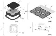
- Figures 3a and 3b show a variant of the embodiment of figure 2a, 2b , or a further particularly preferred embodiment of the fabric memory system 100 described by the present invention.
- the system comprises a "crown" 800 of material suitable for welding the fabric memory system 100 to the head to which it will be destined.
- the layer of thermo-sealing material 800 does not remain positioned under the system 100, but rather forms a crown around the area of installation of the system; the system 100 is fixed to the heat-sealing material layer in turn by means of heat pressing with a temperature range from 100 to 150°C for a period of from 1 to 15 seconds or through ultrasound for an application time from 1 to 12 seconds .
- thermowelded crown which creates a polyurethane layer along the junction with considerable technical and aesthetic improvement.
- the innovative process for digitalizing the fabrics comprises at least the steps of:
- the surface of the fabric 2 remains completely inscribed in the crown 800, the crown 800 (as shown above) remains overlapped by 2.5 mm from the edge of the inner perimeter on the assembly and remains overlapped by 2.5 mm from the external perimeter on the support (whereby said crown 800 remains partially overlapped on the system 100 and partially superimposed on the fabric or support T.
- Figures 4a and 4b show a further particularly preferred embodiment of the fabric memory system 101 described by the present invention; in particular, in this variant, in a particularly advantageous way, the fabric memory system comprises a Lyner 102 instead of a fabric base layer 2, or in this case a film (thickness from 80 microns to 4/5 mm, for example PET) which will be coupled to the dielectric base layer 3 to provide structural support to enable the finished system 101 to be moved.
- the fabric memory system comprises a Lyner 102 instead of a fabric base layer 2, or in this case a film (thickness from 80 microns to 4/5 mm, for example PET) which will be coupled to the dielectric base layer 3 to provide structural support to enable the finished system 101 to be moved.
- the innovative process for digitalizing the fabric described by the present invention comprises at least the steps of:
- both starting coils have equal widths (in this case 50 cm wide reels have been used but the process can be extended to coils even much longer (even 3 meters).
- this operation can be done either by heat press or by heated rollers which couple the melting materials.
- the TPU used is made of a multilayer of polyurethanes with different chemical structures and constructions. Each layer is designed to optimize adhesion with the underlying products.
- the first layers are mainly melting and are usually activated at a temperature around at 80 degrees .. More in detail, the first immediately adheres to the fabric, the second melts at a slightly higher temperature up to the 5th layer that melts at 135°C.
- the upper layers are slightly thicker from 12 to 18 microns and are composed in this way: polyurethane base layer with high temperature resistance, polyurethane layer with the desired color always resistant to temperatures and protective layer also resistant to temperature.
- the concept is analogous to the closing layer 7.
- the melting layers are able to penetrate into the base 3 because the temperature softens the upper layers of this layer and “merges” together the fused layers of the closure 7 with the base 3.
- the waterproofing occurs due to the saturation of the gluing layers inside the fabric and due to the solid conformation of the non-melting states.
- the TPU in order to extrude the TPU there is always need of a PET support to give it a "shape". This supporting film can then be mounted on the TPU or removed to allow further processing.
- the TPU of the base in most of the preferred embodiments is without PET film to eliminate the phase of elimination of the film itself (impossible in the automation phase but to be done by hand).
- the PET layer applied to the finished manufacturing process is applied as protection, and then the final customer will remove it.
- thermo-bi-adhesive layer 80 model 2
- the crown thermo-welding 800 model 3
- this innovative process can be carried out also by reversing the assembly order of the system; that is, it is possible to start from the upper dielectric closing layer, then positioning the rigid module 6 and gluing it (gluing phase) to the aluminum plate 4. Finally, the base TPU layer 3 is coupled.
- the heat press which is normally used has a fixed part in heat-resistant neoprene capable of compressing even 5 -6 mm and a movable part activated by a pneumatic cylinder on which a rigid metal or ceramic material plane is installed. which is heated to the desired temperature. Pressure, temperature, cycle time can be adjusted and, if necessary, also the response of the fixed plane by replacing the neoprene with a less elastic one and therefore less compressible.
- a further variant to the innovative process described herein includes, in particular, the steps of:
- both starting coils have equal widths (in this case 50 cm wide reels have been used, but the process can be extended to coils even much longer (even from 3 meters).
- this operation can be performed either by heat press or by heated rollers which couple the melt materials.
- the fabric may also be in a coil at this stage and the parts of the fabric may be subsequently cut by laser; or it is possible to place the semi-finished products on already cut pieces.
- thermoadhesive in order to make them adhere to the supports with models 2 or 3.
- FIGS 5a and 5b show a further particularly preferred embodiment of the fabric memory system 110 described by the present invention; in particular in this variant, in a particularly advantageous manner, the fabric memory system 110 in this case comprises a base dielectric layer 310 made of kapton, for example of 25 microns or, preferably, of 50 microns.
- the kapton advantageously has the capacity to replace the fabric layer 2 as a supporting structure, since it has characteristics suitable for supporting the system.
- the base fabric 202 can also have any degree of elasticity, that is, significant, so that it is not equal to 0 or substantially zero.
- the innovative process for digitalizing the fabrics described by the present invention comprises at least the steps of:
- the adhesion on the fabric takes place through the TPU overlap of the closing layer, that is, the closing TPU layer 7 has a larger surface than the surfaces of the underlying layers, whereby the surplus surface part is used to fix the system on the fabric of destination.
- the semi-finished product does not adhere to the target fabric.
- thermoadhesive to make the system adhere to the supports, i.e. fabrics T, as described by models 2 and 3.
- two systems 200, 220 comprising a device D, formed here by a base layer 3, foil 4, module 6 and layer of closure of reduced dimensions with respect to the supporting fabric layer 2.
- the electronic area is only 25 x 25 mm compared to a 52 x 55 fabric.
- Cutting can be done by computerized laser. This is advantageous because it is possible to realize not only an "electronic” component but also ornamental solutions printed and with particular geometries.
- the rest is fabric 2 without electronic parts and is lighter and more flexible.
- thermo-sealing solution similar to model 2 or with a thermo-sealing solution similar to model 3.
- figure 8a, b, c, d, (model 8) are represented the steps of the process for the digitalization of the innovative fabrics for the realization in this case of a particularly preferred embodiment, wherein the fabric memory system 300 described by the present invention is achieved by modifying some processing steps.
- a semi-finished product is advantageously comprising at least the base dielectric layer 3 and the aluminum foil 4.
- the module 6 is positioned at a later time.
- this semi-finished product makes it possible to avoid having to handle the aluminum foil autonomously, a factor which (as previously described) causes problems, since the foil is very thin, so fragile and difficult to handle and difficult, to be positioned, the semi-finished product thus made simplifies the movement of the foil 4.
- the base layer TPU 3 can be coupled to a layer or film 103 which is used only to move the various semi-finished parts during processing. On the contrary it would be impossible to transport them because they are not mechanically structured enough to be manipulated accurately.
- the layer 3 of base TPU and the aluminum foil 4 should not "stick” to each other, but only adhere to one another (bonding the two layers would lose the advantage of having a smooth side of the base TPU 3).
- the dies can have cutting footsteps at different heights. This allows the two materials to be etched with different shapes. Removing the scraps from the base TPU 3 and the aluminum foil 4. To remove these scraps, re-roll the roll of TPU and the scrap aluminum, so it is rolled up. only the discarded part, the foils will have their own geometry with a slit, while the base dielectric 3 (for example of a butterfly shape) will have a preferably a formed shape, maintaining a lower surface with respect to the closing dielectric layer 7.
- the film or layer 103 connected to the base layer 3 of support on the other hand, will remain intact, it is not cut to allow the assembly to be dragged.
- a variant provides for obtaining the same result by crossing the base TPU assembly 3/aluminum foil 4 under two different lasers.
- the metals i.e. the aluminum foil in this case
- fiber lasers that operate at a light frequency which does not affect the basic TPU dielectric layer 3.
Landscapes
- Engineering & Computer Science (AREA)
- Physics & Mathematics (AREA)
- General Physics & Mathematics (AREA)
- Theoretical Computer Science (AREA)
- Computer Hardware Design (AREA)
- Microelectronics & Electronic Packaging (AREA)
- Computer Networks & Wireless Communication (AREA)
- Textile Engineering (AREA)
- Laminated Bodies (AREA)
- Laser Beam Processing (AREA)
- Reinforced Plastic Materials (AREA)
- Treatments For Attaching Organic Compounds To Fibrous Goods (AREA)
Claims (6)
- Ein RFID-System (1; 10; 100), das zur Befestigung an Textilien konfiguriert ist, wobei das RFID-System (1; 10; 100) mindestens eine Vorrichtung (D) umfasst, wobei die Vorrichtung (D) Folgendes umfasst:- mindestens eine dielektrische Basisschicht (3);- mindestens eine dielektrische Abdeckschicht (7);- eine leitfähige Folie (4) mit mindestens einem Schlitz (5), wobei die Folie zwischen der mindestens einen dielektrischen Basisschicht (3) und der mindestens einen dielektrischen Abdeckschicht (7) angeordnet ist;- mindestens ein starres elektronisches Modul (6), das eine Antenne umfasst;wobei das RFID-System (1; 10; 100) dadurch gekennzeichnet ist, dass:- das RFID-System (1; 10; 100) ein HF- und/oder ein NFC-RFID-System ist,- das mindestens eine starre elektronische Modul (6), das die Antenne umfasst, zwischen der leitfähigen Folie (4) und der mindestens einen dielektrischen Abdeckschicht (7) angeordnet ist, wobei die Antenne Abmessungen aufweist, die so gewählt sind, dass sie auf den Schlitz (5) passt,- die Vorrichtung (D) mindestens eine Textilschicht (2) umfasst, die die Vorrichtung (D) strukturell unterstützt und auf der Außenseite der mindestens einen dielektrischen Basisschicht (3) angeordnet ist,- der Schlitz (5) länglich und in der Mitte der Folie angeordnet ist, um die Verteilung der magnetischen Feldlinien zu ermöglichen, wodurch die Richtung des magnetischen Feldes umgekehrt wird, wobei das magnetische Feld die leitfähige Folie (4) durch den Schlitz (5) durchquert, wodurch das elektronische Modul (6) aktiviert wird und ein Signal, das von diesem Modul (6) ausgestrahlt wird, verstärkt wird,- die mindestens eine dielektrische Basisschicht (3), das Modul (6), die Folie (4), die mindestens eine dielektrische Abdeckschicht (7) und die Textilschicht (2) miteinander verbunden sind.
- Das RFID-System (1; 10; 100) gemäß Anspruch 1, wobei die mindestens eine dielektrische Basisschicht (3) ein thermoplastisches Polymer oder ein thermoadhäsives Material (TPU) ist, mit mindestens einer Seite, die mit Klebstoff versehen ist, um in die mindestens eine Textilschicht (2) einzudringen, wodurch die Haftung verbessert wird, und in mindestens eine glatte Schicht, um Mikrobewegungen der leitfähigen Folie (4) auf der mindestens einen dielektrischen Basisschicht (3) zu ermöglichen, wodurch die Reaktion des RFID-Systems (1; 10; 100) auf Biegung verbessert wird.
- Das RFID-System (101) gemäß Anspruch 1, wobei die mindestens eine dielektrische Basisschicht (310) aus Kapton besteht, um die Flexibilität des RFID-Systems und die Feuchtigkeitsbeständigkeit des RFID-Systems zu erhöhen, wobei die mindestens eine dielektrische Basisschicht (310) so konfiguriert ist, dass sie als Trägerstruktur für das RFID-System (110) dient, wobei die mindestens eine Textilschicht (202) einen beliebigen Elastizitätsgrad aufweist, der ungleich 0 ist.
- Das RFID-System (1; 300) gemäß den vorhergehenden Ansprüchen, wobei das System (300) ein Halbfertigprodukt umfasst, das die mindestens eine dielektrische Basisschicht (3) und die leitfähige Folie (4) umfasst, wobei die leitfähige Folie (4) eine Aluminiumfolie ist, wodurch die Handhabung der leitfähigen Folie (4) vereinfacht wird.
- Verfahren zur Herstellung eines RFID-Systems (1; 10; 100) gemäß einem der vorhergehenden Ansprüche, wobei das Verfahren mindestens die folgenden Schritte umfasst:- Bildung einer Textilschicht (2) durch Beschichten eines Gewebes oder durch Bearbeiten eines Gewebewbandes, wobei die Textilschicht (2) eine größere Fläche als die Vorrichtung (D) aufweist, um das anschließende Nähen auf ein Empfangsgewebe (T) zu ermöglichen;- Vorformung einer dielektrischen Basisschicht (3) aus thermoadhäsiven oder thermoplastischen Polyurethanen (TPU) mittels Laserschneiden oder mechanischem Schneiden;- Anwenden einer heißen Heißpressung auf die vorgeformte dielektrische Basisschicht (3) für 15 Sekunden bei 55 °C;- Anwenden eines Ultraschallsystems auf die vorgeformte dielektrische Basisschicht (3) für 4 Sekunden bei Raumtemperatur, um die Gesamttemperatur und die Betriebszeiten zu senken;- Vorformung einer Aluminiumfolie (4) mittels Stanzens, Laserschneidens oder mechanischem Schneiden;- Positionieren der vorgeformten Folie (4) und Zentrieren auf der vorgeformten dielektrischen Basisschicht (3) mit einem numerischen Steuerungssystem oder einem Pick- and-Place-System.- Verkleben durch Anbringen eines Klebepunkts, um ein starres elektronisches Modul (6) an der Aluminiumfolie (4) mit einer speziellen Maschine für das Verkleben und Fixieren durch Klebung zu befestigen;- Positionieren des starren elektronischen Moduls (6) mittels eines Pick-and-Place-Systems;- Vorformung einer zweiten dielektrischen Schicht aus TPU, wobei die zweite dielektrische Schicht eine dielektrische Abdeckschicht (7) ist, mittels Stanzens, Laserschneidens oder mechanischem Schneiden;- Positionieren und Wärmeversiegeln der vorgeformten dielektrischen Abdeckschicht (7) bei 155 °C für 15 Sekunden;- Montieren des RFID-Systems (1; 10; 100) durch Nähen;- Formen einer Seite der dielektrischen Abdeckschicht (7) aus TPU;- Drucken der Textilschicht (2) mit einem Logo oder einem Fantasiebild.
- Das Verfahren zur Herstellung eines RFID-Systems (1; 10; 100; 101; 110; 200; 220; 300) gemäß Anspruch 5, wobei das Verfahren die folgenden Schritte umfasst:- Durchführen von Laserschneiden der Folie am Ende des Verfahrens sowohl für die dielektrische Basisschicht (3) als auch für die dielektrische Abdeckschicht (7), wodurch die gleiche Geometrie für die dielektrische Basisschicht (3) und die dielektrische Abdeckschicht (7) erhalten wird, ohne die Funktion des RFID-Systems (1; 10; 100; 101; 110; 200; 220; 300) zu verändern.
Priority Applications (1)
| Application Number | Priority Date | Filing Date | Title |
|---|---|---|---|
| EP23152588.2A EP4221440B1 (de) | 2017-03-23 | 2018-03-22 | Rfid-system zur befestigung an gewebe und verfahren zur digitalisierung von gewebe |
Applications Claiming Priority (2)
| Application Number | Priority Date | Filing Date | Title |
|---|---|---|---|
| IT102017000032017A IT201700032017A1 (it) | 2017-03-23 | 2017-03-23 | Sistema di memoria per tessuti e procedimento per la digitalizzazione di tessuti |
| PCT/IB2018/051944 WO2018172976A1 (en) | 2017-03-23 | 2018-03-22 | Rfid system suitable for being attached to fabrics and method for the digitalization of fabrics |
Related Child Applications (2)
| Application Number | Title | Priority Date | Filing Date |
|---|---|---|---|
| EP23152588.2A Division EP4221440B1 (de) | 2017-03-23 | 2018-03-22 | Rfid-system zur befestigung an gewebe und verfahren zur digitalisierung von gewebe |
| EP23152588.2A Division-Into EP4221440B1 (de) | 2017-03-23 | 2018-03-22 | Rfid-system zur befestigung an gewebe und verfahren zur digitalisierung von gewebe |
Publications (3)
| Publication Number | Publication Date |
|---|---|
| EP3602405A1 EP3602405A1 (de) | 2020-02-05 |
| EP3602405C0 EP3602405C0 (de) | 2025-01-08 |
| EP3602405B1 true EP3602405B1 (de) | 2025-01-08 |
Family
ID=59700002
Family Applications (2)
| Application Number | Title | Priority Date | Filing Date |
|---|---|---|---|
| EP23152588.2A Active EP4221440B1 (de) | 2017-03-23 | 2018-03-22 | Rfid-system zur befestigung an gewebe und verfahren zur digitalisierung von gewebe |
| EP18718511.1A Active EP3602405B1 (de) | 2017-03-23 | 2018-03-22 | Rfid-system zur befestigung an geweben und verfahren zum digitalisieren von geweben |
Family Applications Before (1)
| Application Number | Title | Priority Date | Filing Date |
|---|---|---|---|
| EP23152588.2A Active EP4221440B1 (de) | 2017-03-23 | 2018-03-22 | Rfid-system zur befestigung an gewebe und verfahren zur digitalisierung von gewebe |
Country Status (6)
| Country | Link |
|---|---|
| US (1) | US11663434B2 (de) |
| EP (2) | EP4221440B1 (de) |
| ES (2) | ES3059149T3 (de) |
| IT (1) | IT201700032017A1 (de) |
| PL (2) | PL4221440T3 (de) |
| WO (1) | WO2018172976A1 (de) |
Families Citing this family (24)
| Publication number | Priority date | Publication date | Assignee | Title |
|---|---|---|---|---|
| WO2015145422A1 (en) | 2014-03-26 | 2015-10-01 | Scr Engineers Ltd | Livestock location system |
| US11071279B2 (en) | 2014-09-05 | 2021-07-27 | Intervet Inc. | Method and system for tracking health in animal populations |
| US10986817B2 (en) | 2014-09-05 | 2021-04-27 | Intervet Inc. | Method and system for tracking health in animal populations |
| US11832584B2 (en) | 2018-04-22 | 2023-12-05 | Vence, Corp. | Livestock management system and method |
| FR3086837B1 (fr) | 2018-10-03 | 2021-06-18 | Allflex Europe | Pince pour la manipulation d’un dispositif d’identification d’un animal et/ou de prelevement d’un tissu d’un animal comprenant des moyens de maintien a moyens d’actionnement deportes |
| CN112911927B (zh) | 2018-10-10 | 2023-06-27 | 世亚工程设备有限公司 | 牲畜干乳方法和装置 |
| AU2019428657B2 (en) | 2019-02-08 | 2025-10-23 | Allflex Australia Pty Ltd | Determining the location of an animal |
| AU2019428246A1 (en) | 2019-02-08 | 2021-08-26 | Allflex Australia Pty Ltd | Electronic animal identification tag reader synchronisation |
| AU2019428486B2 (en) | 2019-02-08 | 2025-10-30 | Allflex Australia Pty Ltd | Electronic animal tag reader |
| EP4021650A4 (de) | 2019-08-28 | 2023-09-06 | SCR Engineers Ltd | Vorrichtungen zur analyse eines fluids |
| IL275518B (en) | 2020-06-18 | 2021-10-31 | Scr Eng Ltd | Animal tag |
| USD990062S1 (en) | 2020-06-18 | 2023-06-20 | S.C.R. (Engineers) Limited | Animal ear tag |
| USD990063S1 (en) | 2020-06-18 | 2023-06-20 | S.C.R. (Engineers) Limited | Animal ear tag |
| IL275812B (en) | 2020-07-01 | 2022-01-01 | Scr Eng Ltd | System and method for placing devices |
| WO2022113062A1 (en) | 2020-11-25 | 2022-06-02 | Scr Engineers Ltd. | A system and method for tracing members of an animal population |
| IL280374B2 (en) | 2021-01-24 | 2023-11-01 | Scr Eng Ltd | System and method for controlling animal marking |
| IL280744A (en) | 2021-02-09 | 2022-09-01 | Scr Eng Ltd | A system and method for determining animal population welfare |
| CA206747S (en) | 2021-04-08 | 2024-12-30 | Chevillot Sas | Tag applicator for animals |
| CA206812S (en) | 2021-04-08 | 2023-04-11 | Chevillot Sas | Tag applicator for animals |
| IL283741A (en) | 2021-06-03 | 2022-07-01 | Scr Eng Ltd | A system and method for estimating greenhouse gas emissions in an environment that houses animals |
| WO2022271156A1 (en) * | 2021-06-22 | 2022-12-29 | The American Tights Company Llc | System and management of coated textiles and method of using the same |
| IT202100028706A1 (it) * | 2021-11-11 | 2023-05-11 | Media Contactless Sagl | Etichetta per abbigliamento, procedimento ed impianto per la sua realizzazione |
| US12402596B2 (en) | 2022-05-03 | 2025-09-02 | S.C.R. (Engineers) Limited | Milk channel and feed inlet coupled thereto, and system and method for conserving wash fluid in a washing process for cleaning a milkmeter system |
| IT202300016167A1 (it) * | 2023-08-01 | 2025-02-01 | Spiderweb Tech Srl | Dispositivo con microchip integrabile a indumenti registrabile/leggibile mediante nfc |
Family Cites Families (6)
| Publication number | Priority date | Publication date | Assignee | Title |
|---|---|---|---|---|
| KR101119991B1 (ko) * | 2003-11-04 | 2012-03-15 | 애버리 데니슨 코포레이션 | 향상된 판독 능력을 가지는 고주파 식별 태그 |
| JP4348282B2 (ja) * | 2004-06-11 | 2009-10-21 | 株式会社日立製作所 | 無線用icタグ、及び無線用icタグの製造方法 |
| JP4815891B2 (ja) * | 2005-06-22 | 2011-11-16 | 株式会社日立製作所 | 無線icタグ及びアンテナの製造方法 |
| JP2013152600A (ja) * | 2012-01-25 | 2013-08-08 | Hitachi Chemical Co Ltd | Rfidタグシステム及びrfidパッケージ |
| US20160148086A1 (en) * | 2013-06-19 | 2016-05-26 | Ross Robert Clarke | Radio Frequency Identification Tag |
| EP3014532B1 (de) * | 2013-06-24 | 2020-09-16 | Avery Dennison Corporation | Waschbare robuste etiketten mit einem grossflächigen antennenleiter |
-
2017
- 2017-03-23 IT IT102017000032017A patent/IT201700032017A1/it unknown
-
2018
- 2018-03-22 ES ES23152588T patent/ES3059149T3/es active Active
- 2018-03-22 PL PL23152588.2T patent/PL4221440T3/pl unknown
- 2018-03-22 ES ES18718511T patent/ES3017986T3/es active Active
- 2018-03-22 PL PL18718511.1T patent/PL3602405T3/pl unknown
- 2018-03-22 WO PCT/IB2018/051944 patent/WO2018172976A1/en not_active Ceased
- 2018-03-22 EP EP23152588.2A patent/EP4221440B1/de active Active
- 2018-03-22 US US16/493,762 patent/US11663434B2/en active Active
- 2018-03-22 EP EP18718511.1A patent/EP3602405B1/de active Active
Also Published As
| Publication number | Publication date |
|---|---|
| EP4221440B1 (de) | 2025-10-22 |
| EP3602405C0 (de) | 2025-01-08 |
| US11663434B2 (en) | 2023-05-30 |
| ES3017986T3 (en) | 2025-05-14 |
| EP4221440C0 (de) | 2025-10-22 |
| EP3602405A1 (de) | 2020-02-05 |
| EP4221440A3 (de) | 2023-11-01 |
| US20210232879A1 (en) | 2021-07-29 |
| PL3602405T3 (pl) | 2025-05-12 |
| PL4221440T3 (pl) | 2026-03-09 |
| ES3059149T3 (en) | 2026-03-19 |
| WO2018172976A1 (en) | 2018-09-27 |
| IT201700032017A1 (it) | 2018-09-23 |
| WO2018172976A4 (en) | 2018-11-22 |
| EP4221440A2 (de) | 2023-08-02 |
Similar Documents
| Publication | Publication Date | Title |
|---|---|---|
| EP3602405B1 (de) | Rfid-system zur befestigung an geweben und verfahren zum digitalisieren von geweben | |
| EP3485428B1 (de) | Mehrschichtige elektronische vorrichtung und verfahren zur herstellung und befestigung der vorrichtung | |
| EP3014532B1 (de) | Waschbare robuste etiketten mit einem grossflächigen antennenleiter | |
| US10198677B2 (en) | RFID tag for printed fabric label and method of making | |
| EP2901374B1 (de) | Verbesserungen an rfid-etiketten-anordnungen und verfahren | |
| EP3874410B1 (de) | Ultraschallgeschweisste etikettensysteme und -verfahren | |
| JP3152962U (ja) | 無線周波の識別フラグ | |
| KR102528891B1 (ko) | 메탈 카드 및 카드 제조 방법 | |
| JP5939831B2 (ja) | Rfidタグ | |
| US20110121084A1 (en) | Microcircuit Card Body Forming a Medium for Two Electronic Labels | |
| KR102391551B1 (ko) | 무선 통신 카드 및 그 제조 방법 | |
| US12333360B2 (en) | RFID system suitable for being attached to fabrics and method for the digitalization of fabrics | |
| KR102783844B1 (ko) | 3d 패턴이 형성된 카드 및 그 제조 방법 | |
| EP4639410A1 (de) | Rfid-system für stoffe | |
| US20160129629A1 (en) | Transferring assembly for transferring a radiofrequency identification device onto an object | |
| CN211653663U (zh) | 一种无源无线射频识别标签 | |
| US12321802B2 (en) | Multilayer electronic device and method for the construction and fixing of the device | |
| KR20120002860A (ko) | 폴리에틸렌을 이용한 알에프아이디 태그 및 그 제조방법 | |
| KR101560630B1 (ko) | Rfid 태그 및 그 태그와 케어라벨의 부착방법 | |
| US20250269610A1 (en) | Thermoadhesive multilayer device for a textile | |
| WO2017145079A1 (en) | Electronic device comprising an rfid tag closed in casing, designed for industrial laundry activities, for tracking of objects or animals | |
| CN113392946A (zh) | 一种无源无线射频识别标签及其制造方法 | |
| KR101552815B1 (ko) | 양면 타입의 무선 통신용 태그 제조 장치 | |
| JP2018200635A (ja) | Icタグ,icタグリールおよび品質表示icタグ | |
| KR20100011210U (ko) | 알 에프 아이 디를 구비한 카드 |
Legal Events
| Date | Code | Title | Description |
|---|---|---|---|
| STAA | Information on the status of an ep patent application or granted ep patent |
Free format text: STATUS: UNKNOWN |
|
| STAA | Information on the status of an ep patent application or granted ep patent |
Free format text: STATUS: THE INTERNATIONAL PUBLICATION HAS BEEN MADE |
|
| PUAI | Public reference made under article 153(3) epc to a published international application that has entered the european phase |
Free format text: ORIGINAL CODE: 0009012 |
|
| STAA | Information on the status of an ep patent application or granted ep patent |
Free format text: STATUS: REQUEST FOR EXAMINATION WAS MADE |
|
| 17P | Request for examination filed |
Effective date: 20190920 |
|
| AK | Designated contracting states |
Kind code of ref document: A1 Designated state(s): AL AT BE BG CH CY CZ DE DK EE ES FI FR GB GR HR HU IE IS IT LI LT LU LV MC MK MT NL NO PL PT RO RS SE SI SK SM TR |
|
| AX | Request for extension of the european patent |
Extension state: BA ME |
|
| DAV | Request for validation of the european patent (deleted) | ||
| DAX | Request for extension of the european patent (deleted) | ||
| STAA | Information on the status of an ep patent application or granted ep patent |
Free format text: STATUS: EXAMINATION IS IN PROGRESS |
|
| 17Q | First examination report despatched |
Effective date: 20210506 |
|
| RAP3 | Party data changed (applicant data changed or rights of an application transferred) |
Owner name: EXTERYO S.R.L. |
|
| RAP1 | Party data changed (applicant data changed or rights of an application transferred) |
Owner name: ME INNOVATION SRL |
|
| GRAP | Despatch of communication of intention to grant a patent |
Free format text: ORIGINAL CODE: EPIDOSNIGR1 |
|
| STAA | Information on the status of an ep patent application or granted ep patent |
Free format text: STATUS: GRANT OF PATENT IS INTENDED |
|
| INTG | Intention to grant announced |
Effective date: 20240731 |
|
| GRAS | Grant fee paid |
Free format text: ORIGINAL CODE: EPIDOSNIGR3 |
|
| GRAA | (expected) grant |
Free format text: ORIGINAL CODE: 0009210 |
|
| STAA | Information on the status of an ep patent application or granted ep patent |
Free format text: STATUS: THE PATENT HAS BEEN GRANTED |
|
| AK | Designated contracting states |
Kind code of ref document: B1 Designated state(s): AL AT BE BG CH CY CZ DE DK EE ES FI FR GB GR HR HU IE IS IT LI LT LU LV MC MK MT NL NO PL PT RO RS SE SI SK SM TR |
|
| REG | Reference to a national code |
Ref country code: GB Ref legal event code: FG4D |
|
| REG | Reference to a national code |
Ref country code: CH Ref legal event code: EP |
|
| REG | Reference to a national code |
Ref country code: DE Ref legal event code: R096 Ref document number: 602018078332 Country of ref document: DE |
|
| REG | Reference to a national code |
Ref country code: IE Ref legal event code: FG4D |
|
| U01 | Request for unitary effect filed |
Effective date: 20250203 |
|
| U07 | Unitary effect registered |
Designated state(s): AT BE BG DE DK EE FI FR IT LT LU LV MT NL PT RO SE SI Effective date: 20250207 |
|
| U20 | Renewal fee for the european patent with unitary effect paid |
Year of fee payment: 8 Effective date: 20250409 |
|
| PG25 | Lapsed in a contracting state [announced via postgrant information from national office to epo] |
Ref country code: RS Free format text: LAPSE BECAUSE OF FAILURE TO SUBMIT A TRANSLATION OF THE DESCRIPTION OR TO PAY THE FEE WITHIN THE PRESCRIBED TIME-LIMIT Effective date: 20250408 |
|
| PGFP | Annual fee paid to national office [announced via postgrant information from national office to epo] |
Ref country code: PL Payment date: 20250321 Year of fee payment: 8 |
|
| PGFP | Annual fee paid to national office [announced via postgrant information from national office to epo] |
Ref country code: ES Payment date: 20250402 Year of fee payment: 8 |
|
| PG25 | Lapsed in a contracting state [announced via postgrant information from national office to epo] |
Ref country code: NO Free format text: LAPSE BECAUSE OF FAILURE TO SUBMIT A TRANSLATION OF THE DESCRIPTION OR TO PAY THE FEE WITHIN THE PRESCRIBED TIME-LIMIT Effective date: 20250408 Ref country code: IS Free format text: LAPSE BECAUSE OF FAILURE TO SUBMIT A TRANSLATION OF THE DESCRIPTION OR TO PAY THE FEE WITHIN THE PRESCRIBED TIME-LIMIT Effective date: 20250508 |
|
| PG25 | Lapsed in a contracting state [announced via postgrant information from national office to epo] |
Ref country code: HR Free format text: LAPSE BECAUSE OF FAILURE TO SUBMIT A TRANSLATION OF THE DESCRIPTION OR TO PAY THE FEE WITHIN THE PRESCRIBED TIME-LIMIT Effective date: 20250108 |
|
| PG25 | Lapsed in a contracting state [announced via postgrant information from national office to epo] |
Ref country code: GR Free format text: LAPSE BECAUSE OF FAILURE TO SUBMIT A TRANSLATION OF THE DESCRIPTION OR TO PAY THE FEE WITHIN THE PRESCRIBED TIME-LIMIT Effective date: 20250409 |
|
| PGFP | Annual fee paid to national office [announced via postgrant information from national office to epo] |
Ref country code: CH Payment date: 20250401 Year of fee payment: 8 |
|
| PG25 | Lapsed in a contracting state [announced via postgrant information from national office to epo] |
Ref country code: SM Free format text: LAPSE BECAUSE OF FAILURE TO SUBMIT A TRANSLATION OF THE DESCRIPTION OR TO PAY THE FEE WITHIN THE PRESCRIBED TIME-LIMIT Effective date: 20250108 |
|
| PG25 | Lapsed in a contracting state [announced via postgrant information from national office to epo] |
Ref country code: MC Free format text: LAPSE BECAUSE OF FAILURE TO SUBMIT A TRANSLATION OF THE DESCRIPTION OR TO PAY THE FEE WITHIN THE PRESCRIBED TIME-LIMIT Effective date: 20250108 |
|
| PG25 | Lapsed in a contracting state [announced via postgrant information from national office to epo] |
Ref country code: CZ Free format text: LAPSE BECAUSE OF FAILURE TO SUBMIT A TRANSLATION OF THE DESCRIPTION OR TO PAY THE FEE WITHIN THE PRESCRIBED TIME-LIMIT Effective date: 20250108 |
|
| PG25 | Lapsed in a contracting state [announced via postgrant information from national office to epo] |
Ref country code: SK Free format text: LAPSE BECAUSE OF FAILURE TO SUBMIT A TRANSLATION OF THE DESCRIPTION OR TO PAY THE FEE WITHIN THE PRESCRIBED TIME-LIMIT Effective date: 20250108 |
|
| PLBE | No opposition filed within time limit |
Free format text: ORIGINAL CODE: 0009261 |
|
| STAA | Information on the status of an ep patent application or granted ep patent |
Free format text: STATUS: NO OPPOSITION FILED WITHIN TIME LIMIT |
|
| REG | Reference to a national code |
Ref country code: CH Ref legal event code: L10 Free format text: ST27 STATUS EVENT CODE: U-0-0-L10-L00 (AS PROVIDED BY THE NATIONAL OFFICE) Effective date: 20251119 |
|
| 26N | No opposition filed |
Effective date: 20251009 |
|
| PG25 | Lapsed in a contracting state [announced via postgrant information from national office to epo] |
Ref country code: IE Free format text: LAPSE BECAUSE OF NON-PAYMENT OF DUE FEES Effective date: 20250322 |
|
| REG | Reference to a national code |
Ref country code: CH Ref legal event code: U11 Free format text: ST27 STATUS EVENT CODE: U-0-0-U10-U11 (AS PROVIDED BY THE NATIONAL OFFICE) Effective date: 20260401 |
|
| PGFP | Annual fee paid to national office [announced via postgrant information from national office to epo] |
Ref country code: GB Payment date: 20260311 Year of fee payment: 9 |
|
| U20 | Renewal fee for the european patent with unitary effect paid |
Year of fee payment: 9 Effective date: 20260311 |
|
| PGFP | Annual fee paid to national office [announced via postgrant information from national office to epo] |
Ref country code: TR Payment date: 20260311 Year of fee payment: 9 |