EP3605162A2 - Couche à faible indice de réfraction et dispositif électronique le comprenant - Google Patents
Couche à faible indice de réfraction et dispositif électronique le comprenant Download PDFInfo
- Publication number
- EP3605162A2 EP3605162A2 EP19188682.9A EP19188682A EP3605162A2 EP 3605162 A2 EP3605162 A2 EP 3605162A2 EP 19188682 A EP19188682 A EP 19188682A EP 3605162 A2 EP3605162 A2 EP 3605162A2
- Authority
- EP
- European Patent Office
- Prior art keywords
- layer
- light
- color conversion
- low refractive
- lrl
- Prior art date
- Legal status (The legal status is an assumption and is not a legal conclusion. Google has not performed a legal analysis and makes no representation as to the accuracy of the status listed.)
- Granted
Links
Images


Classifications
-
- G—PHYSICS
- G02—OPTICS
- G02F—OPTICAL DEVICES OR ARRANGEMENTS FOR THE CONTROL OF LIGHT BY MODIFICATION OF THE OPTICAL PROPERTIES OF THE MEDIA OF THE ELEMENTS INVOLVED THEREIN; NON-LINEAR OPTICS; FREQUENCY-CHANGING OF LIGHT; OPTICAL LOGIC ELEMENTS; OPTICAL ANALOGUE/DIGITAL CONVERTERS
- G02F1/00—Devices or arrangements for the control of the intensity, colour, phase, polarisation or direction of light arriving from an independent light source, e.g. switching, gating or modulating; Non-linear optics
- G02F1/01—Devices or arrangements for the control of the intensity, colour, phase, polarisation or direction of light arriving from an independent light source, e.g. switching, gating or modulating; Non-linear optics for the control of the intensity, phase, polarisation or colour
- G02F1/13—Devices or arrangements for the control of the intensity, colour, phase, polarisation or direction of light arriving from an independent light source, e.g. switching, gating or modulating; Non-linear optics for the control of the intensity, phase, polarisation or colour based on liquid crystals, e.g. single liquid crystal display cells
- G02F1/133—Constructional arrangements; Operation of liquid crystal cells; Circuit arrangements
- G02F1/1333—Constructional arrangements; Manufacturing methods
- G02F1/1335—Structural association of cells with optical devices, e.g. polarisers or reflectors
-
- G—PHYSICS
- G02—OPTICS
- G02B—OPTICAL ELEMENTS, SYSTEMS OR APPARATUS
- G02B5/00—Optical elements other than lenses
- G02B5/20—Filters
- G02B5/201—Filters in the form of arrays
-
- G—PHYSICS
- G02—OPTICS
- G02B—OPTICAL ELEMENTS, SYSTEMS OR APPARATUS
- G02B1/00—Optical elements characterised by the material of which they are made; Optical coatings for optical elements
- G02B1/10—Optical coatings produced by application to, or surface treatment of, optical elements
- G02B1/11—Anti-reflection coatings
-
- G—PHYSICS
- G02—OPTICS
- G02B—OPTICAL ELEMENTS, SYSTEMS OR APPARATUS
- G02B6/00—Light guides; Structural details of arrangements comprising light guides and other optical elements, e.g. couplings
- G02B6/0001—Light guides; Structural details of arrangements comprising light guides and other optical elements, e.g. couplings specially adapted for lighting devices or systems
- G02B6/0011—Light guides; Structural details of arrangements comprising light guides and other optical elements, e.g. couplings specially adapted for lighting devices or systems the light guides being planar or of plate-like form
- G02B6/0033—Means for improving the coupling-out of light from the light guide
- G02B6/005—Means for improving the coupling-out of light from the light guide provided by one optical element, or plurality thereof, placed on the light output side of the light guide
-
- G—PHYSICS
- G02—OPTICS
- G02F—OPTICAL DEVICES OR ARRANGEMENTS FOR THE CONTROL OF LIGHT BY MODIFICATION OF THE OPTICAL PROPERTIES OF THE MEDIA OF THE ELEMENTS INVOLVED THEREIN; NON-LINEAR OPTICS; FREQUENCY-CHANGING OF LIGHT; OPTICAL LOGIC ELEMENTS; OPTICAL ANALOGUE/DIGITAL CONVERTERS
- G02F1/00—Devices or arrangements for the control of the intensity, colour, phase, polarisation or direction of light arriving from an independent light source, e.g. switching, gating or modulating; Non-linear optics
- G02F1/01—Devices or arrangements for the control of the intensity, colour, phase, polarisation or direction of light arriving from an independent light source, e.g. switching, gating or modulating; Non-linear optics for the control of the intensity, phase, polarisation or colour
- G02F1/13—Devices or arrangements for the control of the intensity, colour, phase, polarisation or direction of light arriving from an independent light source, e.g. switching, gating or modulating; Non-linear optics for the control of the intensity, phase, polarisation or colour based on liquid crystals, e.g. single liquid crystal display cells
- G02F1/133—Constructional arrangements; Operation of liquid crystal cells; Circuit arrangements
- G02F1/1333—Constructional arrangements; Manufacturing methods
- G02F1/1335—Structural association of cells with optical devices, e.g. polarisers or reflectors
- G02F1/133528—Polarisers
-
- G—PHYSICS
- G02—OPTICS
- G02F—OPTICAL DEVICES OR ARRANGEMENTS FOR THE CONTROL OF LIGHT BY MODIFICATION OF THE OPTICAL PROPERTIES OF THE MEDIA OF THE ELEMENTS INVOLVED THEREIN; NON-LINEAR OPTICS; FREQUENCY-CHANGING OF LIGHT; OPTICAL LOGIC ELEMENTS; OPTICAL ANALOGUE/DIGITAL CONVERTERS
- G02F1/00—Devices or arrangements for the control of the intensity, colour, phase, polarisation or direction of light arriving from an independent light source, e.g. switching, gating or modulating; Non-linear optics
- G02F1/01—Devices or arrangements for the control of the intensity, colour, phase, polarisation or direction of light arriving from an independent light source, e.g. switching, gating or modulating; Non-linear optics for the control of the intensity, phase, polarisation or colour
- G02F1/13—Devices or arrangements for the control of the intensity, colour, phase, polarisation or direction of light arriving from an independent light source, e.g. switching, gating or modulating; Non-linear optics for the control of the intensity, phase, polarisation or colour based on liquid crystals, e.g. single liquid crystal display cells
- G02F1/133—Constructional arrangements; Operation of liquid crystal cells; Circuit arrangements
- G02F1/1333—Constructional arrangements; Manufacturing methods
- G02F1/1335—Structural association of cells with optical devices, e.g. polarisers or reflectors
- G02F1/1336—Illuminating devices
- G02F1/133602—Direct backlight
- G02F1/133606—Direct backlight including a specially adapted diffusing, scattering or light controlling members
- G02F1/133607—Direct backlight including a specially adapted diffusing, scattering or light controlling members the light controlling member including light directing or refracting elements, e.g. prisms or lenses
-
- G—PHYSICS
- G02—OPTICS
- G02F—OPTICAL DEVICES OR ARRANGEMENTS FOR THE CONTROL OF LIGHT BY MODIFICATION OF THE OPTICAL PROPERTIES OF THE MEDIA OF THE ELEMENTS INVOLVED THEREIN; NON-LINEAR OPTICS; FREQUENCY-CHANGING OF LIGHT; OPTICAL LOGIC ELEMENTS; OPTICAL ANALOGUE/DIGITAL CONVERTERS
- G02F1/00—Devices or arrangements for the control of the intensity, colour, phase, polarisation or direction of light arriving from an independent light source, e.g. switching, gating or modulating; Non-linear optics
- G02F1/01—Devices or arrangements for the control of the intensity, colour, phase, polarisation or direction of light arriving from an independent light source, e.g. switching, gating or modulating; Non-linear optics for the control of the intensity, phase, polarisation or colour
- G02F1/13—Devices or arrangements for the control of the intensity, colour, phase, polarisation or direction of light arriving from an independent light source, e.g. switching, gating or modulating; Non-linear optics for the control of the intensity, phase, polarisation or colour based on liquid crystals, e.g. single liquid crystal display cells
- G02F1/133—Constructional arrangements; Operation of liquid crystal cells; Circuit arrangements
- G02F1/1333—Constructional arrangements; Manufacturing methods
- G02F1/1335—Structural association of cells with optical devices, e.g. polarisers or reflectors
- G02F1/1336—Illuminating devices
- G02F1/133615—Edge-illuminating devices, i.e. illuminating from the side
-
- G—PHYSICS
- G02—OPTICS
- G02F—OPTICAL DEVICES OR ARRANGEMENTS FOR THE CONTROL OF LIGHT BY MODIFICATION OF THE OPTICAL PROPERTIES OF THE MEDIA OF THE ELEMENTS INVOLVED THEREIN; NON-LINEAR OPTICS; FREQUENCY-CHANGING OF LIGHT; OPTICAL LOGIC ELEMENTS; OPTICAL ANALOGUE/DIGITAL CONVERTERS
- G02F1/00—Devices or arrangements for the control of the intensity, colour, phase, polarisation or direction of light arriving from an independent light source, e.g. switching, gating or modulating; Non-linear optics
- G02F1/01—Devices or arrangements for the control of the intensity, colour, phase, polarisation or direction of light arriving from an independent light source, e.g. switching, gating or modulating; Non-linear optics for the control of the intensity, phase, polarisation or colour
- G02F1/13—Devices or arrangements for the control of the intensity, colour, phase, polarisation or direction of light arriving from an independent light source, e.g. switching, gating or modulating; Non-linear optics for the control of the intensity, phase, polarisation or colour based on liquid crystals, e.g. single liquid crystal display cells
- G02F1/133—Constructional arrangements; Operation of liquid crystal cells; Circuit arrangements
- G02F1/1333—Constructional arrangements; Manufacturing methods
- G02F1/1335—Structural association of cells with optical devices, e.g. polarisers or reflectors
- G02F1/1336—Illuminating devices
- G02F1/133617—Illumination with ultraviolet light; Luminescent elements or materials associated to the cell
-
- G—PHYSICS
- G02—OPTICS
- G02F—OPTICAL DEVICES OR ARRANGEMENTS FOR THE CONTROL OF LIGHT BY MODIFICATION OF THE OPTICAL PROPERTIES OF THE MEDIA OF THE ELEMENTS INVOLVED THEREIN; NON-LINEAR OPTICS; FREQUENCY-CHANGING OF LIGHT; OPTICAL LOGIC ELEMENTS; OPTICAL ANALOGUE/DIGITAL CONVERTERS
- G02F1/00—Devices or arrangements for the control of the intensity, colour, phase, polarisation or direction of light arriving from an independent light source, e.g. switching, gating or modulating; Non-linear optics
- G02F1/01—Devices or arrangements for the control of the intensity, colour, phase, polarisation or direction of light arriving from an independent light source, e.g. switching, gating or modulating; Non-linear optics for the control of the intensity, phase, polarisation or colour
- G02F1/13—Devices or arrangements for the control of the intensity, colour, phase, polarisation or direction of light arriving from an independent light source, e.g. switching, gating or modulating; Non-linear optics for the control of the intensity, phase, polarisation or colour based on liquid crystals, e.g. single liquid crystal display cells
- G02F1/133—Constructional arrangements; Operation of liquid crystal cells; Circuit arrangements
- G02F1/1333—Constructional arrangements; Manufacturing methods
- G02F1/1335—Structural association of cells with optical devices, e.g. polarisers or reflectors
- G02F1/1336—Illuminating devices
- G02F1/133621—Illuminating devices providing coloured light
-
- H—ELECTRICITY
- H10—SEMICONDUCTOR DEVICES; ELECTRIC SOLID-STATE DEVICES NOT OTHERWISE PROVIDED FOR
- H10K—ORGANIC ELECTRIC SOLID-STATE DEVICES
- H10K59/00—Integrated devices, or assemblies of multiple devices, comprising at least one organic light-emitting element covered by group H10K50/00
- H10K59/80—Constructional details
- H10K59/875—Arrangements for extracting light from the devices
- H10K59/879—Arrangements for extracting light from the devices comprising refractive means, e.g. lenses
-
- B—PERFORMING OPERATIONS; TRANSPORTING
- B32—LAYERED PRODUCTS
- B32B—LAYERED PRODUCTS, i.e. PRODUCTS BUILT-UP OF STRATA OF FLAT OR NON-FLAT, e.g. CELLULAR OR HONEYCOMB, FORM
- B32B2457/00—Electrical equipment
- B32B2457/20—Displays, e.g. liquid crystal displays, plasma displays
-
- B—PERFORMING OPERATIONS; TRANSPORTING
- B32—LAYERED PRODUCTS
- B32B—LAYERED PRODUCTS, i.e. PRODUCTS BUILT-UP OF STRATA OF FLAT OR NON-FLAT, e.g. CELLULAR OR HONEYCOMB, FORM
- B32B2457/00—Electrical equipment
- B32B2457/20—Displays, e.g. liquid crystal displays, plasma displays
- B32B2457/202—LCD, i.e. liquid crystal displays
-
- B—PERFORMING OPERATIONS; TRANSPORTING
- B32—LAYERED PRODUCTS
- B32B—LAYERED PRODUCTS, i.e. PRODUCTS BUILT-UP OF STRATA OF FLAT OR NON-FLAT, e.g. CELLULAR OR HONEYCOMB, FORM
- B32B2457/00—Electrical equipment
- B32B2457/20—Displays, e.g. liquid crystal displays, plasma displays
- B32B2457/206—Organic displays, e.g. OLED
-
- C—CHEMISTRY; METALLURGY
- C09—DYES; PAINTS; POLISHES; NATURAL RESINS; ADHESIVES; COMPOSITIONS NOT OTHERWISE PROVIDED FOR; APPLICATIONS OF MATERIALS NOT OTHERWISE PROVIDED FOR
- C09K—MATERIALS FOR MISCELLANEOUS APPLICATIONS, NOT PROVIDED FOR ELSEWHERE
- C09K2323/00—Functional layers of liquid crystal optical display excluding electroactive liquid crystal layer characterised by chemical composition
- C09K2323/03—Viewing layer characterised by chemical composition
- C09K2323/031—Polarizer or dye
-
- C—CHEMISTRY; METALLURGY
- C09—DYES; PAINTS; POLISHES; NATURAL RESINS; ADHESIVES; COMPOSITIONS NOT OTHERWISE PROVIDED FOR; APPLICATIONS OF MATERIALS NOT OTHERWISE PROVIDED FOR
- C09K—MATERIALS FOR MISCELLANEOUS APPLICATIONS, NOT PROVIDED FOR ELSEWHERE
- C09K2323/00—Functional layers of liquid crystal optical display excluding electroactive liquid crystal layer characterised by chemical composition
- C09K2323/03—Viewing layer characterised by chemical composition
- C09K2323/033—Silicon compound, e.g. glass or organosilicon
-
- G—PHYSICS
- G02—OPTICS
- G02B—OPTICAL ELEMENTS, SYSTEMS OR APPARATUS
- G02B2207/00—Coding scheme for general features or characteristics of optical elements and systems of subclass G02B, but not including elements and systems which would be classified in G02B6/00 and subgroups
- G02B2207/107—Porous materials, e.g. for reducing the refractive index
-
- G—PHYSICS
- G02—OPTICS
- G02F—OPTICAL DEVICES OR ARRANGEMENTS FOR THE CONTROL OF LIGHT BY MODIFICATION OF THE OPTICAL PROPERTIES OF THE MEDIA OF THE ELEMENTS INVOLVED THEREIN; NON-LINEAR OPTICS; FREQUENCY-CHANGING OF LIGHT; OPTICAL LOGIC ELEMENTS; OPTICAL ANALOGUE/DIGITAL CONVERTERS
- G02F1/00—Devices or arrangements for the control of the intensity, colour, phase, polarisation or direction of light arriving from an independent light source, e.g. switching, gating or modulating; Non-linear optics
- G02F1/01—Devices or arrangements for the control of the intensity, colour, phase, polarisation or direction of light arriving from an independent light source, e.g. switching, gating or modulating; Non-linear optics for the control of the intensity, phase, polarisation or colour
- G02F1/13—Devices or arrangements for the control of the intensity, colour, phase, polarisation or direction of light arriving from an independent light source, e.g. switching, gating or modulating; Non-linear optics for the control of the intensity, phase, polarisation or colour based on liquid crystals, e.g. single liquid crystal display cells
- G02F1/133—Constructional arrangements; Operation of liquid crystal cells; Circuit arrangements
- G02F1/1333—Constructional arrangements; Manufacturing methods
- G02F1/1335—Structural association of cells with optical devices, e.g. polarisers or reflectors
- G02F1/133502—Antiglare, refractive index matching layers
-
- H—ELECTRICITY
- H10—SEMICONDUCTOR DEVICES; ELECTRIC SOLID-STATE DEVICES NOT OTHERWISE PROVIDED FOR
- H10K—ORGANIC ELECTRIC SOLID-STATE DEVICES
- H10K2102/00—Constructional details relating to the organic devices covered by this subclass
- H10K2102/301—Details of OLEDs
- H10K2102/331—Nanoparticles used in non-emissive layers, e.g. in packaging layer
-
- H—ELECTRICITY
- H10—SEMICONDUCTOR DEVICES; ELECTRIC SOLID-STATE DEVICES NOT OTHERWISE PROVIDED FOR
- H10K—ORGANIC ELECTRIC SOLID-STATE DEVICES
- H10K59/00—Integrated devices, or assemblies of multiple devices, comprising at least one organic light-emitting element covered by group H10K50/00
- H10K59/30—Devices specially adapted for multicolour light emission
- H10K59/38—Devices specially adapted for multicolour light emission comprising colour filters or colour changing media [CCM]
Definitions
- the present disclosure herein relates to a low refractive layer and an electronic device including the same, and more particularly, to a low refractive layer including hollow inorganic particles, and an electronic device including the same.
- an optical member employing a low refractive material is utilized, and in order to improve the reliability of the electronic devices, it is desirable to develop an optical member having improved durability while maintaining low refractive properties.
- An aspect according to embodiments of the present disclosure is directed toward a low refractive layer having improved strength while exhibiting good low refractive properties, by optimizing the weight ratio of hollow inorganic particles to a matrix.
- An aspect according to embodiments of the present disclosure is also directed toward an electronic device having improved reliability and optical properties by including a low refractive layer with high strength.
- a low refractive layer includes a plurality of hollow inorganic particles, and a matrix configured to fill a space between the plurality of hollow inorganic particles, wherein a weight ratio of the plurality of hollow inorganic particles to the matrix is 4:6 to 7:3.
- the plurality of hollow inorganic particles may be positioned or embedded in a matrix.
- the matrix may also be called a matrix part. This applies also for the following embodiments.
- each of the plurality of hollow inorganic particles may include a core filled with air and a shell surrounding the core, and the shell may be surface-treated with a coupling agent.
- the shell may include an inorganic layer defining the core, an organic layer surrounding an outer surface of the inorganic layer, and a surface treatment layer on an outer surface of the organic layer and including the coupling agent.
- the coupling agent may include a first end coupled to the organic layer, and a second end coupled to the matrix.
- the first end may be an acrylate group and the second end may be a trihydroxysilyl group.
- the coupling agent may be represented by Formula 1 below.
- n is an integer of 1 to 5.
- the shell may include at least one selected from the group consisting of SiO 2 , MgF 2 , and Fe 3 O 4 .
- the shell may have a thickness of 7 nm to 10 nm.
- each of the plurality of hollow inorganic particles may have an average diameter of 20 nm to 200 nm.
- the matrix may include at least one selected from the group consisting of an acrylic-based polymer, a silicone-based polymer, a urethane-based polymer, and an imide-based polymer.
- the low refractive layer may have a transmittance of 95% or greater at a wavelength of 400 nm to 700 nm and a refractive index of 1.1 to 1.5 at a wavelength of 632 nm.
- an electronic device includes a light source configured to provide a first light, a color converter on the light source, and including a first converter configured to wavelength-convert the first light into a second light and a second converter configured to wavelength-convert the first light into a third light, and a low refractive layer on the light source and on at least one of an upper portion and a lower portion of the color converter, wherein the low refractive layer includes a plurality of hollow inorganic particles and a matrix configured to fill a space between the plurality of hollow inorganic particles, and a weight ratio of the plurality of hollow inorganic particles to the matrix is 4:6 to 7:3.
- each of the plurality of hollow inorganic particles may include a core filled with air and a shell surrounding the core, and the shell may be surface-treated with a coupling agent.
- the first light may be blue light
- the first converter may include a first quantum dot configured to covert the blue light into green light
- the second converter may include a second quantum dot configured to convert the blue light into red light
- the electronic device may further include a display element on the color converter.
- the display element may be a liquid crystal display.
- the light source may include a guide panel, and a light source unit on at least one side of the guide panel, and the low refractive layer may be between the guide panel and the color converter.
- the low refractive layer may be directly on the guide panel.
- the electronic device may further include a barrier layer on at least one of an upper surface and a lower surface of the color converter.
- the color converter may include a plurality of color conversion parts spaced apart from each other on a plane, and the plurality of color conversion parts may have a first color conversion part having the first converter, a second color conversion part having the second converter, and a third color conversion part configured to transmit the first light.
- the color converter may further include a light blocking unit between the first, second and third color conversion parts which are spaced apart from each other.
- the electronic device may further include a reflection layer on at least one of an upper portion and a lower portion of the plurality of color conversion parts, and configured to transmit the first light and reflect the second light and the third light.
- the low refractive layer may be between the reflection layer and the plurality of color conversion parts, and configured to cover the plurality of color conversion parts.
- the reflection layer may be between the low refractive layer and the plurality of color conversion parts, and configured to cover the plurality of color conversion parts.
- the color converter may further include a barrier layer on at least one of an upper portion and a lower portion of the plurality of color conversion parts.
- the barrier layer may be between the low refractive layer and the plurality of color conversion parts, and configured to cover the plurality of color conversion parts.
- the color converter may further include an optical filter layer configured to transmit at least one of the second light and the third light.
- the optical filter layer may include a first optical filter layer on the first color conversion part, and a second optical filter layer on the second color conversion part.
- the first optical filter layer may be configured to transmit green light
- the second optical filter layer may be configured to transmit red light
- the electronic device may further include a first base substrate and a second base substrate on the light source, the second base substrate facing the first base substrate, and a liquid crystal layer between the first base substrate and the second base substrate, wherein the color converter may be between the liquid crystal layer and the second base substrate.
- the low refractive layer may be between the liquid crystal layer and the color converter, or between the color converter and the second base substrate.
- the electronic device may further include a first polarizing layer between the light source and the first base substrate, or between the first base substrate and the liquid crystal layer, and a second polarizing layer between the liquid crystal layer and the second base substrate.
- the light source may include an organic electroluminescence element.
- the color converter may further include a dam configured to separate the plurality of color conversion parts from each other, the dam being between adjacent color conversion parts from among the plurality of color conversion parts.
- the color converter may further include a color filter layer on the plurality of color conversion parts, and the color filter layer may include a plurality of filters configured to emit light of different colors, and a light blocking unit configured to separate the plurality of filters from each other, the light blocking unit being between adjacent filters from among the plurality of filters.
- an electronic device includes a display element, a guide panel on a lower portion of the display element, a light source adjacent to at least one side surface of the guide panel, a color converter between the guide panel and the display element, and a low refractive layer between the guide panel and the color converter, wherein the low refractive layer includes a plurality of hollow inorganic particles and a matrix configured to fill a space between the plurality of hollow inorganic particles, and a weight ratio of the plurality of hollow inorganic particles to the matrix is 4:6 to 7:3.
- the light source may include a light emitting element configured to emit blue light
- the color converter may include a green quantum dot configured to be excited by the blue light to emit green light and a red quantum dot configured to be excited by at least one of the blue light and the green light to emit red light.
- the plurality of hollow inorganic particles may include a core filled with air and a shell defining the core, and the shell may include a surface treatment layer including a coupling agent.
- an element when referred to as being "on,” “connected to,” or “coupled to” another element, it may be directly on, connected to, or coupled to the other element or intervening elements or layers may be present.
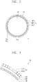
- FIG. 1 is a cross-sectional view of a low refractive layer according to an embodiment of the inventive concept.
- a low refractive layer LRL shown in FIG. 1 may be included in an electronic device DS (see FIG. 7 ) according to an embodiment of the inventive concept to be described later.
- the low refractive layer LRL includes a plurality of hollow inorganic particles HP and a matrix part MX (e.g., a matrix MX).
- the matrix part MX may fill a space between the hollow inorganic particles HP, respectively the hollow inorganic particles HP may be embedded in the matrix part MX.
- the matrix part MX may include a polymer material.
- the matrix part MX may include at least one of an acrylic-based polymer, a silicone-based polymer, a urethane-based polymer, or an imide-based polymer.
- the matrix part MX may include any one polymer material selected from an acrylic-based polymer, a silicone-based polymer, a urethane-based polymer, and an imide-based polymer, or combinations of a plurality of polymer materials selected from the same.
- the matrix part MX may be formed of an acrylic-based resin, a silicone-based resin, a urethane-based resin, and/or an imide-based resin.
- the matrix part MX may be provided by mixing a polymer resin with the hollow inorganic particles HP, and then solidifying the polymer resin in a high-temperature process or in an ultraviolet treatment process.
- the low refractive layer LRL according to an embodiment of the inventive concept includes a plurality of the hollow inorganic particles HP and the matrix part MX, and the weight ratio of the hollow inorganic particles HP to the matrix part MX may be 4:6 to 7:3. That is, when the total weight of the low refractive layer LRL according to an embodiment of the inventive concept is 10 (e.g., 10 parts), the hollow inorganic particles HP may be included in the range of 4 to 7 (e.g., 4 to 7 parts) based on the total weight of the low refractive layer LRL of 10 (e.g., 10 parts). Accordingly, the matrix part MX may be included in the range of 6 to 3 (e.g., 6 to 3 parts) based on the total weight of the low refractive layer LRL of 10 (e.g., 10 parts).
- the refractive index of the low refractive layer LRL is increased so that the optical extraction function of the low refractive layer LRL may be deteriorated in relation to other members.
- the weight of the hollow inorganic particles HP is greater than 7 based on the total weight of the low refractive layer LRL of 10
- the amount of the matrix part MX in the low refractive layer LRL is reduced, therefore, voids and the like (due to insufficient filling between the hollow inorganic particles HP by the matrix part MX) may appear so that the mechanical strength of the low refractive layer LRL may be deteriorated.
- the voids of the low refractive layer LRL may represent a portion that is not filled with the hollow inorganic particles HP or the matrix part MX.
- the hollow inorganic particles HP may be in the form of a core shell.
- FIG. 2 is a cutaway view of a portion of the hollow inorganic particle HP included in the low refractive layer LRL according to an embodiment of the inventive concept.
- FIG. 2 is a drawing for describing the inside of the hollow inorganic particle HP with a portion of the hollow inorganic particle HP being cut away.
- the hollow inorganic particle HP may be, for example, spherical.
- Each of the hollow inorganic particles HP may include a core part (e.g., a core) CR, and a shell part (e.g., a shell) SL surrounding the core part CR.
- the core part CR may be defined or delimited by the shell part SL.
- the shell part SL may be a layer formed of an inorganic material.
- the shell part SL may include at least one of SiO 2 , MgF 2 , or Fe 3 O 4 .
- the hollow inorganic particle HP may be hollow silica.
- the core part CR may be filled with air.
- embodiments of the inventive concept are not limited thereto, and the core part CR in the hollow inorganic particle HP may be filled with a liquid or gas having low refractive properties.
- the shell part SL may be surface-treated with a coupling agent. That is, an outer surface of the shell part SL, i.e., the surface in contact with the matrix part MX, may be treated with the coupling agent.
- FIG. 3 is a cross-sectional view of the hollow inorganic particle HP according to an embodiment of the inventive concept.
- FIG. 4 is a drawing showing a portion of a cross-section of the hollow inorganic particle HP in more detail.
- the shell part SL of the hollow inorganic particle HP may include an inorganic layer IMP, an organic layer OMP, and a surface treatment layer CAP.
- the inorganic layer IMP may define or delimit the core part CR.
- the inorganic layer IMP may include at least one of SiO 2 , MgF 2 , or Fe 3 O 4 .
- the organic layer OMP may surround an outer surface of the inorganic layer IMP.
- the organic layer OMP may be disposed outside of the inorganic layer IMP such that the hollow inorganic particles HP may be dispersed and arranged in the matrix part MX. That is, the organic layer OMP allows the hollow inorganic particles HP to be uniformly dispersed in the matrix part MX without being clustered together.
- the shell part SL of the hollow inorganic particle HP may include the surface treatment layer CAP.
- the surface treatment layer CAP may be disposed on an outer surface of the organic layer OMP.
- the outer surface of the organic layer OMP may be adjacent to the matrix part MX.
- the surface treatment layer CAP may surround the outer surface of the organic layer OMP.
- the surface treatment layer CAP may include a coupling agent CA.
- the surface treatment layer CAP may be a layer formed by coating the organic layer OMP with the coupling agent CA.
- the coupling agent CA may include a first end EG1 coupled to the organic layer OMP, and a second end EG2 coupled to the matrix part MX.
- the first end EG1 may be chemically coupled to the organic layer OMP, and the second end EG2 may be chemically coupled to the matrix part MX.
- the first end EG1 of the coupling agent CA may be an acrylate group, and the second end EG2 may be a trihydroxysilyl group.
- the coupling agent CA may be represented by Formula 1 below.
- n may be an integer of 1 to 5.
- the coupling agent CA may be 2-(trihydroxysilyl)ethyl methacrylate, and/or the like, but embodiments of the inventive concept are not limited thereto.
- the average diameter of the hollow inorganic particles HP may be 20 nm to 200 nm.
- a diameter D HP of the hollow inorganic particles HP may be the outermost diameter of the shell part SL.
- a thickness D SL of the shell part SL may be 7 nm to 10 nm.
- the strength of the hollow inorganic particles HP may be maintained while increasing (e.g., maximizing) the volume of the core part CR.
- the hollow inorganic particles HP may adjust the refractive index of the low refractive layer LRL by filling the core part CR with air, or by including a low refractive material in the core part CR.
- the refractive index of the hollow inorganic particles HP may be 1.0 to 1.3.
- the low refractive layer LRL of an embodiment has a transmittance of 95% or greater in a visible light region having a wavelength range of 400 nm to 700 nm, and a refractive index of 1.1 to 1.5 at a wavelength of 632 nm.
- the low refractive layer LRL of an embodiment of the inventive concept may exhibit improved strength by enhancing (e.g., optimizing) the weight ratio of the hollow inorganic particles HP to the matrix part MX.
- the low refractive layer LRL of an embodiment of the inventive concept may exhibit high mechanical strength by adjusting the weight ratio of the hollow inorganic particles HP to the matrix part MX to be 4:6 to 7:3, and surface-treating the hollow inorganic particles HP with the coupling agent CA so as to increase the coupling force with the matrix part MX and to reduce or minimize void generation.
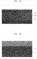
- FIG. 5A and FIG. 5B are images showing a cross-sectional state (e.g., cross-sectional view) of a low refractive layer according to a comparative example and an example respectively.
- a low refractive layer LRL' of the comparative example of FIG. 5A has a weight ratio of hollow inorganic particles to a matrix part of 9:1, and because the matrix part fails to sufficiently fill the space between the hollow inorganic particles, there are many voids VD.
- the low refractive layer LRL of the example of FIG. 5B (e.g., utilizing the same hollow inorganic particles and the same matrix material as the comparative example of FIG. 5A ) has a weight ratio of hollow inorganic particles to a matrix part of 6:4, and there are no voids VD observed as in the comparative example. That is, the low refractive layer LRL of an embodiment of the inventive concept has a desirable (e.g., optimizes the) weight ratio of the hollow inorganic particles HP to the matrix part MX to reduce or minimize void generation, thereby exhibiting improved strength of a film.
- FIG. 6 shows the results of adhesion force values measured by a strength test (e.g., Stud Pull Test) when a low refractive layer according to a Comparative Example and a low refractive layer according to Examples 1 and 2 were respectively utilized.
- Samples utilized in the test were prepared by laminating a glass substrate/a low refraction layer/a siloxane inorganic layer, and the strength of the low refractive layer in the Comparative Example and Examples 1-2 were relatively compared.
- the Comparative Example was prepared by utilizing a low refractive layer in which the ratio of hollow inorganic particles to a matrix part was 9:1, and a shell part of the hollow inorganic particles included only an inorganic layer and an organic layer.
- Example 1 was prepared similarly to the Comparative Example except for utilizing a low refractive layer in which the ratio of hollow inorganic particles to a matrix part was 6:4.
- Example 2 was prepared by utilizing a low refractive layer in which the ratio of hollow inorganic particles to a matrix part was 6:4, and a shell part of the hollow inorganic particles included an inorganic layer, an organic layer, and a surface treatment layer disposed on the outside of the organic layer.
- Example 2 higher adhesion force was observed in Examples 1-2 than in the Comparative Example.
- the average value of adhesion force was about 8.4 MPa, and in Example 1, the average value of adhesion force was about 60.36 MPa.
- the average value of adhesion force was about 79.6 MPa. That is, from the adhesion force values of the Comparative Example and Examples 1-2, it can be confirmed that the low refractive layer of an embodiment of the inventive concept has excellent strength.
- hollow inorganic particles having a surface treatment layer were included to increase the coupling strength between the matrix part and the hollow inorganic particles, so that the adhesion force value was higher when compared with that of Example 1.
- a low refractive layer of an embodiment of the inventive concept enhances (e.g., optimizes) the weight ratio of hollow inorganic particles to a matrix part such that spaces between the hollow inorganic particles are sufficiently filled by the matrix part so as to reduce or minimize void generation.
- the low refractive layer of an embodiment of the inventive concept surface-treats the hollow inorganic particles with a coupling agent so as to increase the coupling force with the matrix part.
- the low refractive layer of an embodiment of the inventive concept exhibited improved internal strength while having a good low refractive index.
- FIG. 7 is an exploded perspective view of an electronic device DS according to an embodiment of the inventive concept.
- the electronic device DS of an embodiment may include various elements, such as a display element (e.g., a display), a touch element, and/or a detection element, activated according to an electric signal.
- the electronic device DS of an embodiment may include a window member WP, a display member DP, and a housing member HAU.
- the electronic device DS includes a display element, and may be a display device providing images.
- the electronic device DS may be a liquid crystal display device or an organic electroluminescence element.
- a first direction axis DR1 to a third direction axis DR3 are shown.
- Direction axes described in the present specification are relative, and for convenience of explanation, the direction of the third direction axis DR3 may be defined as the direction in which an image is provided to a user.
- the terms such as an "upper surface,” an “upper portion,” a “lower surface,” or a “lower portion” refer to the relative position of surfaces or portions along the third direction axis DR3 as shown in FIG. 7 .
- first direction axis DR1 and a second direction axis DR2 cross (e.g., are orthogonal to) each other, and the third direction axis DR3 may be normal with respect to a plane defined by the first direction axis DR1 and the second direction axis DR2.
- the plane defined by the first direction axis DR1 and the second direction axis DR2 may be a display surface on which an image is provided.
- the window member WP may be disposed on the display member DP.
- the window member WP may be made of a material including glass, sapphire, or plastic.
- the window member WP includes a light transmitting region TA, which transmits an image provided from the display member DP, and a light blocking region BA, which is adjacent to the light transmitting region TA and in which an image is not transmitted.
- the light transmitting region TA may be disposed at the center of the electronic device DS on the plane defined by the first direction axis DR1 and the second direction axis DR2.
- the light blocking region BA may be disposed on the periphery of the light transmitting region TA and has a shape of a frame surrounding the light transmitting region TA.
- the window member WP may include only the light transmitting region TA, in which case the light blocking region BA may be omitted.
- the light blocking region BA may be disposed on at least one side of the light transmitting region TA.
- the window member WP may be omitted.
- the display member DP may be disposed on a lower portion (e.g., on the bottom) of the window member WP.
- the display member DP may include a liquid crystal display element or an organic electroluminescence element.
- a surface of the display member DP i.e., the surface on which an image is displayed, is defined as a display surface.
- the display surface includes a display region DA on which an image is displayed, and a non-display region NDA on which an image is not displayed.
- the display region DA may be defined at the center of the display member DP on the plane and may overlap the light transmitting region TA of the window member WP.
- the housing member HAU may be disposed at a lower portion (e.g., on the bottom) of the display member DP to house the display member DP.
- the housing member HAU may be disposed to cover the display member DP such that the upper surface of the display member DP, which is the display surface, is to be exposed.
- the housing member HAU may cover a side surface and the lower surface of the display member DP such that the entire upper surface thereof is to be exposed.
- the housing member HAU may cover a portion of the upper surface as well as the side surface and the lower surface of the display member DP.
- the electronic device DS of an embodiment may include the low refractive layer LRL of an embodiment described with reference to FIGS. 1-6 .
- the electronic device DS of an embodiment may include a light source member, a color conversion member disposed on the light source member, and the low refractive layer LRL of an embodiment disposed between the light source member and the color conversion member.
- the low refractive layer LRL included in the electronic device DS of an embodiment may convert (e.g., redirect) a path of light.
- the low refractive layer LRL may be utilized to extract light in relation to adjacent layers or members.
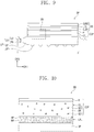
- FIG. 8 is an exploded perspective view of a display member included in an electronic device of an embodiment of the inventive concept.
- FIGS. 9 and 10 are cross-sectional views showing a portion of a display member according to an embodiment of the inventive concept.
- FIG. 9 is a cross-sectional view taken along the line I-I' shown in FIG. 8
- FIG. 10 a cross-sectional view showing the BB region of FIG. 9 .
- the display member DP may include a light source member (e.g., a light source) LP and a display element (e.g., a display) DD.
- the display member DP may include a color conversion member (e.g., a color converter) CCP disposed on the light source member LP and the low refractive layer LRL disposed between the light source member LP and the color conversion member CCP.
- the light source member LP may include a light source unit LU and a guide panel GP.
- the light source unit LU may provide a first light.
- the light source unit LU may include a circuit board PB and a light emitting element LD disposed (e.g., mounted) on the circuit board PB.
- the circuit board PB may provide power to the mounted light emitting element LD.
- the circuit board PB may provide a dimming signal and a driving voltage to the mounted light emitting element LD.
- the circuit board PB may include at least one insulating layer and at least one circuit layer.
- the circuit board PB may be a metal core printed circuit board.
- each light emitting element LD may have a structure in which an n-type semiconductor layer, an active layer, and a p-type semiconductor layer are sequentially laminated.
- Each light emitting element LD may include a light emitting diode for generating light. When the driving voltage is applied, electrons and holes are recombined while moving in the light emitting diode.
- the plurality of light emitting elements LD may emit light of the same wavelength range.
- the light source unit LU may include a plurality of light emitting elements LD for emitting light of different wavelength ranges.
- the light emitting element LD may emit the first light having a central wavelength in a wavelength range of about 440 nm to 460 nm.
- the light emitting element LD may emit blue light.
- the light source member LP may include a guide panel GP.
- the light source unit LU may be disposed on at least one side of the guide panel GP.
- the first light emitted from the light source unit LU may be incident on at least one side of the guide panel GP and provided to the display element DD.
- the blue light emitted from the light emitting element LD is incident on the guide panel GP and transmitted to the color conversion member CCP, and light (of which wavelength has been converted in the color conversion member CCP) may be provided to the display element DD.
- one side of the guide panel GP adjacent to the light source unit LU is shown as having an inclined cross-section toward one side surface adjacent to the light source unit LU, but embodiments of the inventive concept are not limited thereto.
- the guide panel GP may include a material having high light transmittance in the visible light region.
- the guide panel GP may include glass.
- the guide panel GP may be made of a transparent polymer resin, such as polymethyl methacrylate (PMMA).
- PMMA polymethyl methacrylate
- the guide panel GP may have a refractive index of about 1.4 to 1.55.
- the light emitted from the light emitting element LD may be incident on the guide panel GP.
- a light outgoing pattern part e.g., a light outgoing pattern
- the light outgoing pattern part CP is provided on the lower surface of the guide panel GP, and may have a shape convexly protruding toward the housing member HAU (see FIG. 7 ).
- the light outgoing pattern part CP may have a shape of a convex lens protruding toward the housing member HAU, but embodiments of the inventive concept are not limited thereto.
- the light outgoing pattern part CP may be formed of a material having a different refractive index value from that of the guide panel GP.
- the light outgoing pattern part CP may transmit the light emitted from the light source unit LU and incident on one side of the guide panel GP to the other side of the guide panel GP, or may change the direction of light such that the light incident in the direction of the lower surface of the guide panel GP is transmitted in the direction of a light outgoing surface, which is the upper surface of the guide panel GP.
- the light outgoing pattern part CP changes the path of light provided to the lower surface of the guide panel GP such that the light is emitted toward the display element DD.
- the low refractive layer LRL may be disposed on the light source member LP. Referring to FIGS. 8-10 , the low refractive layer LRL may be disposed on the guide panel GP.
- the low refractive layer LRL includes the plurality of hollow inorganic particles HP and the matrix part MX.
- the same contents e.g., the same descriptions
- the weight ratio of the hollow inorganic particles HP to the matrix part MX may be 4:6 to 7:3.
- a surface of the hollow inorganic particles HP, the surface of which is adjacent the matrix part MX may be treated with a coupling agent.
- the low refractive layer LRL may be directly provided on the guide panel GP.
- the low refractive layer LRL may be formed by being coated on the guide panel GP.
- the plurality of the hollow inorganic particles HP are mixed with a polymer resin, which disperses the same (e.g., the plurality of the hollow inorganic particles HP are dispersed in the polymer resin), and provided (e.g., coated) on the guide panel GP, and then the polymer resin is solidified to form the low refractive layer LRL including the plurality of the hollow inorganic particles HP and the matrix part MX.
- Examples of a coating method for forming the low refractive layer LRL include slit coating, spin coating, roll coating, spray coating, and inkjet printing, but a method for providing the low refractive layer LRL is not limited thereto.
- the low refractive layer LRL may be directly provided on the guide panel GP by utilizing various suitable methods such as a transfer method.
- the refractive index of the low refractive layer LRL may be lower than the refractive index of the guide panel GP.
- the refractive index of the low refractive layer LRL may be lower than the refractive index of the color conversion member CCP provided on the low refractive layer LRL.
- the difference in the refractive index of the low refractive layer LRL and the refractive index of the guide panel GP may be 0.2 or greater.
- the low refractive layer LRL may have a refractive index lower than that of the guide panel GP such that light incident on the guide panel GP from the light source unit LU may be effectively transmitted to the other side of the guide panel GP, which is relatively spaced apart from the light source unit LU.
- a capping layer may be further disposed on the low refractive layer LRL.
- the capping layer may be a protection layer for protecting the low refractive layer LRL.
- the capping layer may be an inorganic material layer including at least one inorganic material selected from silicon nitride, silicon oxide, and silicon oxynitride.
- the capping layer may be directly disposed on the low refractive layer LRL.
- the capping layer may be formed of a single layer or a plurality of layers.
- the color conversion member CCP may be disposed on the low refractive layer LRL.
- the color conversion member CCP is disposed between the light source member LP and the display element DD, and may include converters QD1 and QD2 for wavelength-converting (e.g., for converting the wavelength of) the first light provided from the light source unit LU.
- the color conversion member CCP may include the first converter QD1 for wavelength-converting the first light (e.g., having a first wavelength) into a second light (e.g., having a second wavelength) and the second converter QD2 for wavelength-converting the first light into a third light (e.g., having a third wavelength).
- the color conversion member CCP may include a color conversion layer CCL including the first converter QD1 and the second converter QD2 and a barrier layer BL disposed on at least one of the upper surface and the lower surface of the color conversion layer CCL. That is, the barrier layer BL may be disposed on at least one of the upper surface and the lower surface of the color conversion member CCP.
- the barrier layer BL may serve to reduce or prevent penetration of moisture and/or oxygen (hereinafter, referred to as 'moisture/oxygen').
- the barrier layer BL may be disposed on the color conversion layer CCL to prevent or substantially prevent the color conversion layer CCL from being exposed to moisture/oxygen.
- the barrier layer BL may cover the color conversion layer CCL.
- the barrier layer BL may include at least one inorganic layer. That is, the barrier layer BL may include an inorganic material.
- the barrier layer BL may include silicon nitride, aluminum nitride, zirconium nitride, titanium nitride, hafnium nitride, tantalum nitride, silicon oxide, aluminum oxide, titanium oxide, tin oxide, cerium oxide and/or silicon oxynitride, a metal thin film having light transmittance, and/or the like.
- the barrier layer BL may further include an organic film.
- the barrier layer BL may be formed of a single layer or a plurality of layers.
- the color conversion layer CCL may be directly disposed on the low refractive layer LRL.
- the barrier layer BL may be omitted on the lower surface on the color conversion layer CCL.
- the low refractive layer LRL may serve as the barrier layer BL on the lower surface of the color conversion layer CCL.
- the barrier layer BL may cover the color conversion layer CCL on (e.g., the upper surface of) the color conversion layer CCL.
- the color conversion member CCP may include the first converter QD1 for wavelength-converting the first light provided from the light source unit LU into green light and the second converter QD2 for wavelength-converting the first light into red light.
- the first light may be blue light, but is not limited thereto.
- the second converter QD2 may be excited by the second light.
- the first converter QD1 may be (or include) a green quantum dot excited by the blue light, which is the first light, to emit green light, which is the second light.
- the second converter QD2 may be (or include) a red quantum dot excited by at least one of the blue light, which is the first light, and the green light, which is the second light, to emit red light.
- a quantum dot may be a particle for wavelength-converting the light provided from the light source unit LU.
- a quantum dot is a material having a crystal structure of a few nanometers in size, and is composed of hundreds to thousands of atoms. Due to a small size thereof, a quantum dot exhibits a quantum confinement effect in which an energy band gap is increased. When light having a higher energy than the bandgap is incident on a quantum dot, the quantum dot is excited by absorbing the light, and then falls to a ground state by emitting light of a specific wavelength.
- the wavelength of the emitted light has a value corresponding to the band gap.
- the size and composition of a quantum dot is adjusted, light emitting properties caused by the quantum confinement effect may be adjusted.
- the color of emitted light may be changed.
- the particle size of a quantum dot is smaller, light of the shorter wavelength region may be emitted.
- the particle size of a quantum dot for emitting green light may be smaller than the particle size of a quantum dot for emitting red light.
- a quantum dot may be selected from Group II-VI compounds, Group III-V compounds, Group IV-VI compounds, Group IV elements, Group IV compounds, and combinations thereof.
- the Group II-VI compounds may be selected from a binary compound selected from CdSe, CdTe, ZnS, ZnSe, ZnTe, ZnO, HgS, HgSe, HgTe, MgSe, MgS, and mixtures thereof, a ternary compound selected from CdSeS, CdSeTe, CdSTe, ZnSeS, ZnSeTe, ZnSTe, HgSeS, HgSeTe, HgSTe, CdZnS, CdZnSe, CdZnTe, CdHgS, CdHgSe, CdHgTe, HgZnS, HgZnSe, HgZnTe, MgZnSe, MgZnS, and mixtures thereof, and a quaternary compound selected from HgZnTeS, CdZnSeS, CdZnSeTe, CdZnSTe,
- the Group III-V compounds may be selected from a binary compound selected from GaN, GaP, GaAs, GaSb, AlN, AlP, AlAs, AlSb, InN, InP, InAs, InSb, and mixtures thereof, a ternary compound selected from GaNP, GaNAs, GaNSb, GaPAs, GaPSb, AlNP, AlNAs, AlNSb, AlPAs, AlPSb, InNP, InNAs, InNSb, InPAs, InPSb, GaAlNP, and mixtures thereof, and a quaternary compound selected from GaAlNAs, GaAlNSb, GaAlPAs, GaAlPSb, GaInNP, GaInNAs, GaInNSb, GaInPAs, GaInPSb, InAlNP, InAlNAs, InAlNSb, InAlPAs, InAlPSb, and mixtures thereof.
- the Group IV-VI compounds may be selected from a binary compound selected from SnS, SnSe, SnTe, PbS, PbSe, PbTe, and mixtures thereof, a ternary compound selected from SnSeS, SnSeTe, SnSTe, PbSeS, PbSeTe, PbSTe, SnPbS, SnPbSe, SnPbTe, and mixtures thereof, and a quaternary compound selected from SnPbSSe, SnPbSeTe, SnPbSTe, and mixtures thereof.
- the Group IV elements may be selected from Si, Ge, and mixtures thereof.
- the Group IV compounds may be a binary compound selected from SiC, SiGe, and mixtures thereof.
- a binary compound, a ternary compound, or a quaternary compound may be present in a particle in a uniform concentration, or may be present in the same particle in a concentration partially different from each other's. In other words, a binary compound, a ternary compound, or a quaternary compound may be present in a particle in a nonuniform concentration.
- a quantum dot may have a core-shell structure in which a core and a shell surrounding the core are included.
- one quantum dot having a core-shell structure may surround another quantum dot.
- the interface of the core and the shell may have a concentration gradient in which the concentration of an element present in the shell becomes lower toward the center.
- a quantum dot may be a particle having a nanometer scale size.
- the quantum dot may have a full width of half maximum (FWHM) of a light emission wavelength spectrum of about 45 nm or less, for example, about 40 nm or less, or about 30 nm or less, and the color purity and/or color reproducibility may be improved in the above ranges.
- FWHM full width of half maximum
- light emitted through the quantum dot is emitted in all directions so that a wide viewing angle may be realized (e.g., the viewing angle may be improved or widened).
- the form of the quantum dot is not particularly limited as long as it is a form commonly utilized in the art, the quantum dot in the form of spherical, pyramidal, multi-arm, cubic nanoparticles, nanotubes, nanowires, nanofibers, nanoparticles, and/or the like may be utilized.
- the display element DD may be provided with white light.
- light emitted from the light source unit LU, transmitted through the color conversion member CCP, and then provided to the display element DD may be white light. That is, the display element DD may be provided with mixed light of the blue light provided from the light source unit LU, the green light emitted from the first converter QD1, and the red light emitted from the second converter QD2.
- the color conversion member CCP may include the first converter QD1, the second converter QD2, and a base resin BR.
- the base resin BR is a medium in which the first and second converters QD1 and QD2 are dispersed, and may be made of various suitable resin compositions which may be generally referred to as a binder. However, embodiments of the inventive concept are not limited thereto. In the present specification, any suitable medium capable of dispersing and disposing the first and second converters QD1 and QD2 may be referred to as the base resin BR regardless of the name, additional other functions, constituent materials, and/or the like thereof.
- the base resin BR may be a polymer resin.
- the base resin BR may be an acrylic-based resin, a urethane-based resin, a silicone-based resin, an epoxy-based resin, and/or the like.
- the base resin BR may be a transparent resin.
- the display member DP of an embodiment may have improved durability by including the low refractive layer LRL with improved strength of the embodiment described above between the guide panel GP and the color conversion member CCP. That is, the electronic device DS (see FIG. 7 ) including the display member DP of an embodiment has good optical properties and may exhibit improved durability and reliability.
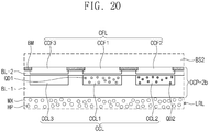
- FIG. 11 shows another embodiment of a display member included in the electronic device DS (see FIG. 7 ) of an embodiment.
- FIG. 12 is a top view showing a portion of a color conversion member included in the display member of FIG. 11 .
- FIG. 13 is a cross-sectional view taken along the line II-II' shown in FIG. 11 .
- FIG. 14 is a cross-sectional view showing the CC region of FIG. 13 .
- FIG. 15 is a cross-sectional view showing another example of a portion included in the display member of FIG. 11 .
- FIG. 15 may be a cross-sectional view of another embodiment corresponding to the CC region of FIG. 14 .
- a display member DP-1 of an embodiment may include a first base substrate BS1 and a second base substrate BS2 facing each other, and a liquid crystal layer LCL disposed between the first base substrate BS1 and the second base substrate BS2. That is, the display member DP-1 of an embodiment includes a display element DD-1 disposed on a light source member LP-1, and the display element DD-1 may be a liquid crystal display element including the liquid crystal layer LCL between the first and second base substrates BS1 and BS2 facing each other.
- the display element DD-1 may include a color conversion member (e.g., a color converter) CCP-1.
- the color conversion member CCP-1 may be disposed on the liquid crystal layer LCL.
- the display element DD-1 may include a first substrate SUB1 relatively adjacent to the light source member LP-1 and a second substrate SUB2 facing the first substrate SUB1 (with the liquid crystal layer LCL interposed therebetween) and including the color conversion member CCP-1.
- the light source member LP-1 may be a backlight unit which provides light to the display element DD-1.
- the light source member LP-1 may be a direct (e.g., direct type) backlight unit or an edge (e.g., edge type) backlight unit, and/or the like, but embodiments of the inventive concept are not limited thereto. Any suitable light source member which provides light to the display element DD-1 may be utilized without limitation.
- the light source member LP-1 may provide a first light to the display element DD-1.
- the light source member LP-1 may provide blue light to the display element DD-1.
- the first substrate SUB1 may include the first base substrate BS1 and a circuit layer CL provided on the first base substrate BS1.
- the first base substrate BS1 may be a member which provides a base surface on which the circuit layer CL is disposed.
- the first base substrate BS1 may be a glass substrate, a metal substrate, a plastic substrate, and/or the like.
- the first base substrate BS1 may be an inorganic layer, an organic layer, or a composite material layer.
- the circuit layer CL is disposed on the first base substrate BS1, and the circuit layer CL may include a plurality of transistors.
- the transistors may each include a control electrode, an input electrode, and an output electrode.
- the circuit layer CL may include a switching transistor, a driving transistor and/or the like to drive the display element DD-1.
- the display element DD-1 may further include a first polarizing layer PL and a second polarizing layer ICP.
- the first polarizing layer PL may be included in the first substrate SUB1. Referring to FIG. 11 and FIG. 13 , in an embodiment, the first polarizing layer PL may be disposed on the lower surface of the first base substrate BS1. However, embodiments of the inventive concept are not limited thereto.
- the first polarizing layer PL may be disposed on an upper portion (e.g., on top) of the first base substrate BS1, and may be disposed between the liquid crystal layer LCL and the first base substrate BS1.
- the first polarizing layer PL may be provided as a separate member, or may include a polarizer formed by coating or deposition.
- the first polarizing layer PL may be formed by coating a material including a dichroic dye and a liquid crystal compound.
- the first polarizing layer PL may include a wire grid polarizer.
- the second substrate SUB2 facing the first substrate SUB1 may include the second base substrate BS2, the color conversion member CCP-1, and the low refractive layer LRL.
- the second substrate SUB2 may further include a reflection layer RP, a planarization layer OC, and the second polarizing layer ICP.
- the second base substrate BS2 may be a member which provides a base surface on which the color conversion member CCP-1 is disposed.
- the second base substrate BS2 may be a glass substrate, a metal substrate, a plastic substrate, and/or the like.
- the second base substrate BS2 may be an inorganic layer, an organic layer, or a composite material layer.
- the color conversion member CCP-1 may include a plurality of color conversion parts (e.g., a plurality of color converters) CCL1, CCL2, and CCL3 spaced apart from each other on a plane.
- the color conversion member CCP-1 may further include a light blocking unit BM disposed between the first to third color conversion parts CCL1, CCL2, and CCL3.
- the plurality of color conversion parts CCL1, CCL2, and CCL3 may be disposed to be spaced apart from each other on the plane defined by the first direction axis DR1 and the second direction axis DR2.
- the first to third color conversion parts CCL1, CCL2, and CCL3, which emit light of different colors, may be disposed side by side while being spaced apart from each other, and in the second direction axis DR2 direction, color conversion parts which emit light of the same color may be disposed side by side while being spaced apart from each other.
- the light blocking unit BM is disposed, and the light blocking unit BM may be a black matrix.
- the light blocking unit BM may include an organic light blocking material or an inorganic shielding material, each including a black pigment and/or a black dye.
- the light blocking unit BM may reduce or prevent a light leakage phenomenon and may distinguish the boundaries between the adjacent color conversion parts CCL1, CCL2, and CCL3.
- the light blocking unit BM may be disposed to overlap the neighboring color conversion parts CCL1, CCL2, and CCL3. That is, on a plane defined by the first direction axis DR1 and the third direction axis DR3, the light blocking unit BM may be disposed such that a portion thereof overlaps the neighboring color conversion parts CCL1, CCL2, and CCL3 in the thickness direction.
- the color conversion member CCP-1 may include the first converter QD1 for absorbing the first light and wavelength-converting the first light into the second light and the second converter QD2 for absorbing the first light and wavelength-converting the first light into the third light.
- the first light may be blue light
- the second light may be green light
- the third light may be red light.
- the first converter QD1 and the second converter QD2 included in the color conversion member CCP-1 may be applied thereto.
- the first converter QD1 may be (or include) a green quantum dot
- the second converter QD2 may be (or include) a red quantum dot.
- the color conversion member CCP-1 may include a first color conversion part (e.g., a first converter) CCL1 including the first converter QD1, a second color conversion part (e.g., a second converter) CCL2 including the second converter QD2, and a third color conversion part (e.g., a third converter) CCL3 for transmitting the first light.
- the first converter QD1 may absorb the first light, which is blue light, and emit green light
- the second converter QD2 may absorb the first light, which is blue light, and emit red light. That is, the first color conversion part CCL1 may be the first light emitting region which emits green light, and the second color conversion part CCL2 may be the second light emitting region which emits red light.
- the third color conversion part CCL3 may not include a color converter.
- the third color conversion part CCL3 may transmit the first light (e.g., first color light) provided from the light source member LP-1. That is, the third color conversion part CCL3 may transmit blue light.
- the third color conversion part CCL3 may be formed of a polymer resin.
- the third color conversion part CCL3 may be an acrylic-based resin, a urethane-based resin, a silicone-based resin, an epoxy-based resin, and/or the like.
- the third color conversion part CCL3 may be formed of a transparent resin, or an opaque (e.g., a white) resin.
- the first to third color conversion parts CCL1, CCL2, and CCL3 may be provided on the second base substrate BS2.
- the first to third color conversion parts CCL1, CCL2, and CCL3 may be patterned and provided on one surface of the second base substrate BS2.
- the first to third color conversion parts CCL1, CCL2, and CCL3 may be provided on the lower surface of the second base substrate BS2.
- the low refractive layer LRL may be provided between the light source member LP-1 and the color conversion member CCP-1.
- the same contents e.g., the same descriptions
- the low refractive layer LRL of the embodiment described with reference to FIGS. 1-6 may be applied thereto.
- the low refractive layer LRL may include the plurality of hollow inorganic particles HP (see FIG. 1 ) and the matrix part MX (see FIG. 1 ) in a weight ratio of 4:6-7:3.
- an outer surface of the hollow inorganic particles HP may be treated with a coupling agent.
- the low refractive layer LRL may be disposed on a lower portion (e.g., on the bottom) of the color conversion member CCP-1 to change the direction of light which is emitted from the color conversion member CCP-1 and direct it toward an upper portion of the display member DP-1.
- the low refractive layer LRL may be disposed on a lower portion of the color conversion member CCP-1 to serve an optical extraction function for reflecting the light emitted from the color conversion member CCP-1 back to proceed in an upper direction of the display member DP-1. Accordingly, the display member DP-1 of an embodiment may exhibit improved durability and increased optical efficiency.
- the low refractive layer LRL may be disposed on an upper portion (e.g., on top) of the color conversion member CCP-1.
- the second substrate SUB2 may further include the reflection layer RP.
- the reflection layer RP may be disposed between the color conversion member CCP-1 and the liquid crystal layer LCL.
- the reflection layer RP may transmit the first light, and may reflect the second and third light.
- the reflection layer RP may be a selective transmissive reflective layer.
- the reflection layer RP may transmit the first light provided from the light source member LP-1, and may reflect the second and third light emitted from the color conversion parts CCL1, CCL2, and CCL3 of the color conversion member CCP-1 and direct them toward a lower portion of the display member DP-1 so as to be emitted in an upper direction of the display member DP-1.
- the reflection layer RP may be a single layer, or a laminate of a plurality of insulating films.
- the reflection layer RP may include a plurality of insulating films (e.g., laminated over one another), so that the range of transmission and reflection wavelengths may be determined depending on the refractive index difference between the laminated layers, the thickness of each of the laminated layers, and the number of laminated layers, and/or the like.
- the reflection layer RP may include a first insulating film and a second insulating film which have different refractive indexes.
- the reflection layer RP may include at least one first insulating film and at least one second insulating film.
- Each of the first insulating film and the second insulating film may be provided in a plurality and alternately laminated.
- an insulating film having a relatively high refractive index a metal oxide material may be utilized.
- an insulating film of a high refractive index may include at least one of SiNx, TiOx, TaOx, HfOx, or ZrOx.
- an insulating film having a relatively low refractive index may include SiOx and/or SiCOx.
- the reflection layer RP may be formed by alternately and repetitively depositing SiNx and SiOx.
- the reflection layer RP may be disposed on a lower portion (e.g., on the bottom) of the low refractive layer LRL.
- the low refractive layer LRL may be disposed between the reflection layer RP and the color conversion parts CCL1, CCL2, and CCL3, and cover the color conversion parts CCL1, CCL2, and CCL3.
- the reflection layer RP may be disposed on an upper portion (e.g., on top) of the low refractive layer LRL.
- a color conversion member CCP-1a, the reflection layer RP, and the low refractive layer LRL may be sequentially disposed on the second base substrate BS2. That is, the reflection layer RP is disposed between the low refractive layer LRL and the color conversion parts CCL1, CCL2, and CCL3, and the reflection layer RP may cover the color conversion parts CCL1, CCL2, and CCL3.
- the color conversion members CCP-1 and CCP-1a may further include optical filter layers FP1 and FP2 disposed on the color conversion layer CCL including the first to third color conversion parts CCL1, CCL2, and CCL3.
- the optical filter layers FP1 and FP2 may be disposed on the color conversion layer CCL including the first to third color conversion parts CCL1, CCL2, and CCL3, and may block the first light and transmit the second and/or third light. That is, the optical filter layers FP1 and FP2 may block blue light, and may transmit green light and red light.
- the optical filter layers FP1 and FP2 may be disposed on the first and second color conversion parts CCL1 and CCL2, and may not be disposed on the third color conversion part CCL3.
- the optical filter layers FP1 and FP2 may be composed of a single layer, or may be a laminate of a plurality of layers.
- the optical filter layers FP1 and FP2 may be a single layer including a material for absorbing blue light, or may have a structure in which an insulating layer of a low refractive index (such as the reflection layer RP) and an insulating layer of a high refractive index are laminated.
- the optical filter layers FP1 and FP2 may include a pigment and/or a dye to block light of a specific wavelength.
- the optical filter layers FP1 and FP2 may be a yellow color filter layer which absorbs blue light in order to block the blue light.
- the optical filter layers FP1 and FP2 may include a first optical filter layer FP1 disposed on the first color conversion part CCL1, and a second optical filter layer FP2 disposed on the second color conversion part CCL2.
- the first optical filter layer FP1 may be a filter layer which blocks blue light and transmits green light.
- the second optical filter layer FP2 may be a filter layer which blocks blue light and transmits red light.
- the second substrate may further include the planarization layer OC.
- the reflection layer RP and/or the low refractive layer LRL may be disposed to surround concave and convex parts of the color conversion parts CCL1, CCL2, and CCL3. That is, in a process of producing the display member DP-1 according to an embodiment, the reflection layer RP and/or the low refractive layer LRL may be provided on the color conversion parts CCL1, CCL2, and CCL3 after the color conversion parts CCL1, CCL2, and CCL3 are disposed.
- the refection layer RP and/or the low refractive layer LRL are disposed along the concave and convex parts of the color conversion parts CCL1, CCL2, and CCL3 to have concave and convex parts corresponding to concave and convex parts of the color conversion layer CCL (including the color conversion parts CCL1, CCL2, and CCL3).
- the planarization layer OC may be disposed on a lower portion (e.g., on the bottom) of the reflection layer RP and/or the low refractive layer LRL.
- the planarization layer OC may be disposed to surround concave and convex parts of the reflection layer RP and the low refractive layer LRL.
- the planarization layer OC may be disposed to fill the concave and convex parts on the lower surface of the reflection layer RP or the low refractive layer LRL to planarize a surface adjacent to the second polarizing layer ICP, which is adjacent to the liquid crystal layer LCL.
- the second polarizing layer ICP may be included in the second substrate SUB2.
- the second polarizing layer ICP may be disposed between the liquid crystal layer LCL and the color conversion member CCP-1.
- the second polarizing layer ICP may be a polarizing layer in the form of an in-cell.
- the second polarizing layer ICP may be formed by coating a material including a dichroic dye and a liquid crystal compound.
- the second polarizing layer ICP may be a wire grid polarizing layer.
- the low refractive layer LRL was described to be disposed on a lower portion (e.g., on the bottom) of the color conversion members CCP-1 and CCP-1a, but embodiments of the inventive concept are not limited thereto.
- the low refractive layer LRL may be disposed on an upper portion (e.g., on top) of the color conversion members CCP-1 and CCP-1a.
- the low refractive layer LRL may be disposed on the upper portion of the color conversion parts CCL1, CCL2, and CCL3 to increase optical efficiency of light emitted to the outside.
- the low refractive layer LRL of the embodiment described above with improved strength is utilized, so that improved durability may be achieved.
- the low refractive layer LRL is included on the upper portion of the color conversion members CCP-1 and CCP-1a to increase optical efficiency in the display member DP-1. That is, the electronic device DS (see FIG. 7 ) including the display member DP-1 of an embodiment has improved durability and reliability and may exhibit high optical efficiency.
- FIG. 16 shows another embodiment of a display member included in the electronic device DS (see FIG. 7 ) of an embodiment.
- FIG. 17 is a cross-sectional view taken along the line III-III' shown in FIG. 16 .
- FIG. 18 is a cross-sectional view showing the EE region of FIG. 17 .
- FIG. 19 and FIG. 20 are cross-sectional views showing another example of a portion included in the display member of FIG. 16 .
- a display member DP-2 of an embodiment may include a light source member (e.g., a light source) LP-2, the low refractive layer LRL provided on the light source member LP-2, and a color conversion member (e.g., a color converter) CCP-2 provided on the low refractive layer LRL.
- the display member DP-2 of an embodiment may include an organic electroluminescence element.
- the light source member LP-2 may include an organic electroluminescence element OEL.
- the display member DP-2 may include the first base substrate BS1, a circuit layer CL-2, and a sealing member TFE.
- the first base substrate BS1 may be a member for providing a base surface on which the organic electroluminescence element OEL is disposed.
- the first base substrate BS1 may be a glass substrate, a metal substrate, a plastic substrate, and/or the like.
- embodiments of the inventive concept are not limited thereto, and the first base substrate BS1 may be an inorganic layer, an organic layer, or a composite material layer.
- the circuit layer CL-2 is disposed on the first base substrate BS1, and the circuit layer CL-2 may include a plurality of transistors.
- the transistors may each include a control electrode, an input electrode, and an output electrode.
- the circuit layer CL-2 may include a switching transistor, a driving transistor and the like to drive the organic electroluminescence element OEL.
- the organic electroluminescence element OEL may be provided on the circuit layer CL-2.
- the organic electroluminescence element OEL may include a first electrode EL1 and a second electrode EL2 facing each other, and a plurality of organic layers disposed between the first electrode EL1 and the second electrode EL2.
- the organic electroluminescence element OEL may include a hole transport region HTR, a light emitting layer EML, and an electron transport region ETR disposed between the first electrode EL1 and the second electrode EL2.
- the organic electroluminescence element OEL may emit the first light.
- the organic electroluminescence element OEL may emit blue light.
- the light emitting layer EML of the organic electroluminescence element OEL may be provided as a common layer on the first base substrate BS1.
- the light emitting layer EML may be patterned and provided (e.g., in the form of a plurality of separated regions).
- the light emitting layer EML may be patterned by being separated (e.g., divided) by a pixel defining layer PDL.
- the light emitting layer EML may be patterned to correspond to each of the first to third color conversion parts CCL1, CCL2, and CCL3.
- the sealing member TFE may be included, and the sealing member TFE may be disposed on the second electrode EL2.
- the sealing member TFE may be directly disposed on the second electrode EL2.
- the sealing member TFE may be a single layer, or a laminate of a plurality of layers.
- the sealing member TFE may be a thin film sealing layer.
- the sealing member TFE protects the organic electroluminescence element OEL.
- the sealing member TFE may cover the organic electroluminescence element OEL.
- the organic electroluminescence element OEL may be sealed by the sealing member TFE.
- the sealing member TFE may include at least one organic film and at least one inorganic film.
- the least one organic film and the at least one inorganic film may be alternately disposed.
- the sealing member TFE may include two inorganic films and an (e.g., one) organic film disposed between the two inorganic films.
- the inorganic film may include an inorganic material such as aluminum oxide and/or silicon nitride, and the organic film may include an acrylate-based organic material.
- the color conversion member CCP-2 may be disposed on the light source member LP-2 including the organic electroluminescence element OEL.
- the low refractive layer LRL may be provided between the light source member LP-2 and the color conversion member CCP-2.
- the same contents e.g., the same descriptions
- the low refractive layer LRL may include the plurality of hollow inorganic particles HP and the matrix part MX in a weight ratio of 4:6-7:3.
- the outer surface of the hollow inorganic particles HP may be treated with a coupling agent.
- the low refractive layer LRL may be disposed on a lower portion (e.g., on the bottom) of the color conversion member CCP-2 to change the direction of light which is emitted from the color conversion member CCP-2 and direct it toward an upper portion of the display member DP-2.
- the low refractive layer LRL may be disposed on a lower portion of the color conversion member CCP-2 to serve an optical extraction function for reflecting the light emitted from the color conversion member CCP-2 back to proceed in an upper direction of the display member DP-2. Accordingly, the display member DP-2 of an embodiment may exhibit improved durability and increased optical efficiency.
- the low refractive layer LRL may be disposed on an upper portion of the color conversion member CCP-2.
- the color conversion member CCP-2 may include the plurality of color conversion parts CCL1, CCL2, and CCL3 spaced apart from each other on a plane.
- the color conversion member CCP-2 may further include the light blocking unit BM disposed between the first to third color conversion parts CCL1, CCL2, and CCL3.
- the light blocking unit BM may be disposed corresponding to the pixel defining layer PDL.
- the color conversion member CCP-2 may include the color conversion layer CCL composed of the plurality of color conversion parts CCL1, CCL2, and CCL3.
- the color conversion parts CCL1, CCL2, and CCL3 and the light blocking unit BM the same description of the color conversion parts CCL1, CCL2, and CCL3 and the light blocking unit BM included in the display member DP and DP-1 of the embodiment described with reference to FIGS. 8-15 may be applied thereto.
- the color conversion member CCP-2 may include the first converter QD1 for absorbing the first light and wavelength-converting the first light into the second light and the second converter QD2 for absorbing the first light and wavelength-converting the first light into the third light.
- the color conversion member CCP-2 may include the first color conversion part CCL1 including the first converter QD1, the second color conversion part CCL2 including the second converter QD2, and the third color conversion part CCL3 for transmitting the first color light.
- the barrier layer BL may further be disposed.
- the barrier layer BL may be disposed on at least one of the upper portion and the lower portion of the color conversion layer CCL included in the color conversion member CCP-2 to prevent or substantially prevent the color conversion layer CCL from being exposed to moisture/oxygen. Also, the barrier layer BL may cover the color conversion layer CCL.
- the barrier layer BL may include at least one inorganic layer.
- the color conversion layer CCL may be directly disposed on the low refractive layer LRL. In this case, on the lower surface of the color conversion layer CCL, the barrier layer BL may be omitted.
- the display member DP-2 of an embodiment may include the second base substrate BS2.
- the second base substrate BS2 faces the first base substrate BS1 and may be a member which provides a base surface on which the color conversion member CCP-2 is disposed.
- the second base substrate BS2 may be a glass substrate, a metal substrate, a plastic substrate, and/or the like.
- embodiments of the inventive concept are not limited thereto, and the second base substrate BS2 may be an inorganic layer, an organic layer, or a composite material layer.
- FIG. 19 is a cross-sectional view showing another example of a portion included in the display member DP-2 of the embodiment of FIG. 16 , which shows another example of a portion corresponding to the EE region of FIG. 17 .
- a color conversion member e.g., a color converter
- CCP-2a a color conversion member
- the color conversion member CCP-2a may also include the light blocking unit BM and a dam part (e.g., a dam) DM between the color conversion parts CCL1, CCL2, and CCL3.
- the dam part DM is disposed to overlap the light blocking unit BM and may be disposed between the color conversion parts CCL1, CCL2, and CCL3.
- the dam part DM may be formed by utilizing a polymer resin.
- the dam part DM may be formed by patterning utilizing an acrylic-based resin, an imide-based resin, and/or the like. After the dam part DM is patterned, spaces between the dam parts DM may be filled with the color conversion parts CCL1, CCL2, and CCL3. The dam part DM may distinguish the neighboring color conversion parts CCL1, CCL2, and CCL3 from each other.
- the optical filter layer FP may be disposed on the first color conversion part CCL1 and the second color conversion part CCL2.
- the optical filter layer FP may block the first light and transmit the second and/or third light. That is, the optical filter layer FP may block blue light and transmit green light and red light.
- the optical filter layers FP1 and FP2 may be disposed on the first and second color conversion parts CCL1 and CCL2, and may not be disposed on the third color conversion part CCL3.
- the optical filter layer FP of the embodiment shown in FIG. 19 may be integrally provided on the first and second color conversion parts CCL1 and CCL2, when compared with the optical filter layers FP1 and FP2 included in the color conversion member CCP-1 of the embodiment described with reference to FIGS. 13 and 14 .
- the optical filter layer FP may be provided to overlap the first color conversion part CCL1, the second color conversion part CCL2, and the light blocking unit BM adjacent thereto.
- embodiments of the inventive concept are not limited thereto.
- the optical filter layer FP may be provided in plurality while being spaced apart from one another on a plane so as to correspond to each of the first color conversion part CCL1, and the second color conversion part CCL2.
- the reflection layer RP may be disposed between the low refractive layer LRL and the color conversion member CCP-2a.
- the same contents as those for the reflection layer RP included in the display member DP-1 of the embodiment described with reference to FIGS. 11-15 may be applied thereto.
- the reflection layer RP disposed on a lower portion of the color conversion member CCP-2a of an embodiment may transmit the first light provided from the light source member LP-2, and may reflect the second and third light.
- the reflection layer RP may be a selective transmissive reflective layer.
- the low refractive layer LRL may be directly disposed on a lower portion of the color conversion parts CCL1, CCL2, and CCL3.
- the low refractive layer LRL may be disposed between the reflection layer RP and the color conversion parts CCL1, CCL2, and CCL3.
- FIG. 20 is a cross-sectional view showing another example of a portion included in the display member DP-2 of the embodiment of FIG. 16 , i.e., showing another example of a portion corresponding to the EE region of FIG. 17 .
- a color conversion member e.g., a color converter
- CCP-2b is disposed on the low refractive layer LRL, and may include the color conversion layer CCL including the plurality of color conversion parts CCL1, CCL2, and CCL3 and a color filter layer CFL disposed on the color conversion layer CCL.
- the color filter layer CFL may include a first filter part (e.g., a first filter) CCF1 overlapping the first color conversion part CCL1, a second filter part (e.g., a second filter) CCF2 overlapping the second color conversion part CCL2, and a third filter part (e.g., a third filter) CCF3 overlapping the third color conversion part CCL3.
- a first filter part e.g., a first filter
- CCF1 overlapping the first color conversion part CCL1
- a second filter part e.g., a second filter
- CCF3 overlapping the third color conversion part CCL3.
- the color filter layer CFL may reduce or prevent reflection caused by external light.
- the color filter layer CFL having the first filter part CCF1, which is a green filter, the second filter part CCF2, which is a red filter, and the third filter part CCF3, which is a blue filter, may transmit light provided from each of the first color conversion part CCL1, the second color conversion part CCL2, and the third color conversion part CCL3, respectively, and block light other than the light provided from a corresponding color conversion part.
- the color conversion member CCP-2a may further include barrier layers BL-1 to BL-2 disposed on the upper portion and the lower portion of the color conversion parts CCL1, CCL2, and CCL3.
- the barrier layers BL-1 to BL-2 may protect the color conversion parts CCL1, CCL2, and CCL3.
- the same contents e.g., the same descriptions
- the barrier layers BL-1 to BL-2 may include at least one inorganic layer.
- a first barrier layer BL-1 may be disposed between the low refractive layer LRL and the color conversion parts CCL1, CCL2, and CCL3, and a second barrier layer BL-2 may be disposed between the color conversion parts CCL1, CCL2, and CCL3 and the color filter layer CFL. At least one of the first barrier layer BL-1 and the second barrier layer BL-2 may be omitted.
- the low refractive layer LRL was described to be disposed on a lower portion of the color conversion members CCP-2, CCP-2a, and CCP-2b, but embodiments of the inventive concept are not limited thereto.
- the low refractive layer LRL may be disposed on an upper portion of the color conversion members CCP-2, CCP-2a, and CCP-2b.
- the low refractive layer LRL may be disposed on the upper portion of the color conversion parts CCL1, CCL2, and CCL3 to increase optical efficiency of light emitted to the outside.
- the low refractive layer LRL of the embodiment described above with improved strength is included, so that improved durability may be achieved.
- the low refractive layer LRL is included on the upper portion or the lower portion of the color conversion members CCP-2, CCP-2a, and CCP-2b to increase optical extraction efficiency. That is, the electronic device DS (see FIG. 7 ) including the display member DP-2 of an embodiment has improved durability and reliability and may exhibit high optical efficiency.
- An electronic device of an embodiment includes a low refractive layer in which the ratio of hollow inorganic particles to a matrix part is enhanced (e.g., optimized), thereby exhibiting reliability (e.g., improved reliability).
- an electronic device of an embodiment includes the low refractive layer in which the ratio of hollow inorganic particles to a matrix part is enhanced (e.g., optimized) in the display member, thereby exhibiting good optical efficiency and high durability.
- a low refractive layer of an embodiment of the inventive concept enhances (e.g., optimizes) the weight ratio of hollow inorganic particles to a matrix part to reduce or minimize the ratio (e.g., amount) of voids inside (e.g., inside the low refractive layer) while maintaining a low refractive index, thereby exhibiting high strength.
- An electronic device of an embodiment includes the low refractive layer in which the ratio of hollow inorganic particles to a matrix part is enhanced (e.g., optimized) to exhibit high optical efficiency and color reproducibility, thereby achieving improved display quality.
Landscapes
- Physics & Mathematics (AREA)
- Nonlinear Science (AREA)
- General Physics & Mathematics (AREA)
- Optics & Photonics (AREA)
- Mathematical Physics (AREA)
- Chemical & Material Sciences (AREA)
- Crystallography & Structural Chemistry (AREA)
- Electroluminescent Light Sources (AREA)
- Liquid Crystal (AREA)
- Planar Illumination Modules (AREA)
- Optical Elements Other Than Lenses (AREA)
- Optical Filters (AREA)
- Polarising Elements (AREA)
- Surface Treatment Of Optical Elements (AREA)
- Inorganic Compounds Of Heavy Metals (AREA)
- Electrochromic Elements, Electrophoresis, Or Variable Reflection Or Absorption Elements (AREA)
- Devices For Indicating Variable Information By Combining Individual Elements (AREA)
Applications Claiming Priority (1)
| Application Number | Priority Date | Filing Date | Title |
|---|---|---|---|
| KR1020180088924A KR102518416B1 (ko) | 2018-07-31 | 2018-07-31 | 저굴절층 및 이를 포함하는 전자 장치 |
Publications (3)
| Publication Number | Publication Date |
|---|---|
| EP3605162A2 true EP3605162A2 (fr) | 2020-02-05 |
| EP3605162A3 EP3605162A3 (fr) | 2020-05-13 |
| EP3605162B1 EP3605162B1 (fr) | 2022-12-14 |
Family
ID=67439128
Family Applications (1)
| Application Number | Title | Priority Date | Filing Date |
|---|---|---|---|
| EP19188682.9A Active EP3605162B1 (fr) | 2018-07-31 | 2019-07-26 | Couche à faible indice de réfraction et dispositif électronique le comprenant |
Country Status (6)
| Country | Link |
|---|---|
| US (1) | US11650363B2 (fr) |
| EP (1) | EP3605162B1 (fr) |
| JP (1) | JP7389581B2 (fr) |
| KR (1) | KR102518416B1 (fr) |
| CN (1) | CN110794489B (fr) |
| TW (1) | TWI835828B (fr) |
Cited By (2)
| Publication number | Priority date | Publication date | Assignee | Title |
|---|---|---|---|---|
| EP3929998A1 (fr) * | 2020-06-23 | 2021-12-29 | Samsung Display Co., Ltd. | Unité de filtre couleur et appareil d'affichage la comportant |
| US12016233B2 (en) | 2020-09-28 | 2024-06-18 | Samsung Display Co., Ltd. | Display device |
Families Citing this family (18)
| Publication number | Priority date | Publication date | Assignee | Title |
|---|---|---|---|---|
| KR102551221B1 (ko) | 2018-09-03 | 2023-07-04 | 삼성디스플레이 주식회사 | 광학 부재 및 이를 포함하는 표시 장치 |
| KR102825491B1 (ko) * | 2019-07-31 | 2025-06-27 | 삼성디스플레이 주식회사 | 표시 장치 |
| KR102787866B1 (ko) * | 2020-03-19 | 2025-04-01 | 삼성디스플레이 주식회사 | 디스플레이 장치 |
| KR102815702B1 (ko) * | 2020-06-05 | 2025-06-04 | 삼성디스플레이 주식회사 | 색 제어 부재 및 이를 포함하는 표시 장치 |
| KR102951882B1 (ko) | 2020-06-09 | 2026-04-14 | 삼성디스플레이 주식회사 | 표시장치 및 이의 제조 방법 |
| KR102867995B1 (ko) | 2020-08-14 | 2025-10-02 | 삼성디스플레이 주식회사 | 디스플레이 장치 |
| KR102731962B1 (ko) * | 2020-09-08 | 2024-11-20 | 동우 화인켐 주식회사 | 적층체, 상기 적층체의 제조방법 및 상기 적층체를 포함하는 화상표시장치 |
| KR20230106602A (ko) * | 2020-10-09 | 2023-07-13 | 오티아이 루미오닉스 인크. | 낮은 지수 코팅 및 방사선 수정 층을 포함하는 디바이스 |
| CN112382733A (zh) * | 2020-11-16 | 2021-02-19 | 京东方科技集团股份有限公司 | 一种柔性显示面板、柔性显示装置以及制作方法 |
| CN112820837B (zh) * | 2021-01-05 | 2022-09-09 | 武汉华星光电半导体显示技术有限公司 | 一种显示面板 |
| WO2022186034A1 (fr) * | 2021-03-01 | 2022-09-09 | 日本化薬株式会社 | Composition de résine pour couper la lumière bleue à l'aide de particules d'oxyde métallique creuses, et son utilisation |
| JP7121223B1 (ja) * | 2021-03-01 | 2022-08-17 | 日本化薬株式会社 | 金属酸化物中空粒子を用いたブルーライトカット用樹脂組成物及びその用途 |
| KR20220129721A (ko) * | 2021-03-16 | 2022-09-26 | 삼성디스플레이 주식회사 | 수지 조성물, 이를 이용한 표시 장치 |
| CN115207196B (zh) * | 2021-04-12 | 2025-10-24 | 群创光电股份有限公司 | 显示面板 |
| CN113174230B (zh) * | 2021-04-23 | 2022-10-11 | 山东理工大学 | 一种用于布料激光焊接的硅溶胶树脂及其制备方法和应用 |
| KR20230012132A (ko) * | 2021-07-14 | 2023-01-26 | 삼성디스플레이 주식회사 | 표시 장치 |
| KR102707559B1 (ko) * | 2021-09-30 | 2024-09-20 | 삼성디스플레이 주식회사 | 잉크 조성물 및 상기 잉크 조성물로 제조된 층을 포함하는 디스플레이 장치 |
| JP2023069198A (ja) * | 2021-11-05 | 2023-05-18 | 信越化学工業株式会社 | 波長変換体及びそれを用いた波長変換材料 |
Family Cites Families (59)
| Publication number | Priority date | Publication date | Assignee | Title |
|---|---|---|---|---|
| WO2006030823A1 (fr) | 2004-09-15 | 2006-03-23 | Dai Nippon Printing Co., Ltd. | Feuille de controle d'un angle de visualisation et ecran |
| JP2006299248A (ja) | 2005-03-22 | 2006-11-02 | Fuji Photo Film Co Ltd | 無機微粒子含有組成物、光学フィルム、反射防止フィルム、それを用いた偏光板および表示装置 |
| US7691459B2 (en) * | 2005-03-22 | 2010-04-06 | Fujifilm Corporation | Inorganic fine particle-containing composition, optical film, antireflection film and polarizing film, and polarizing plate and display device using the same |
| JP4946016B2 (ja) * | 2005-11-25 | 2012-06-06 | 富士ゼロックス株式会社 | 多色表示用光学組成物、光学素子、及び光学素子の表示方法 |
| US20080199667A1 (en) * | 2007-02-16 | 2008-08-21 | Samsung Electronics Co., Ltd. | Magnetic field controlled active reflector and magnetic display panel comprising the active reflector |
| JP2009108262A (ja) | 2007-10-31 | 2009-05-21 | Nof Corp | 含フッ素硬化性塗液及びそれを用いた減反射材 |
| KR20090086192A (ko) * | 2009-07-22 | 2009-08-11 | 주식회사 나노브릭 | 광결정성을 이용한 표시 방법 및 장치 |
| KR101678649B1 (ko) | 2010-09-27 | 2016-11-23 | 삼성디스플레이 주식회사 | 표시 장치 및 이의 제조 방법 |
| EP2638321B1 (fr) * | 2010-11-10 | 2019-05-08 | Nanosys, Inc. | Films constitués de points quantiques, dispositifs d'éclairage et procédés d'éclairage |
| JP5693944B2 (ja) * | 2010-12-22 | 2015-04-01 | 旭化成ケミカルズ株式会社 | 成膜性を有する有機−無機複合体及びその製造方法 |
| JP5987693B2 (ja) | 2011-01-20 | 2016-09-07 | 日油株式会社 | 透過率向上フィルム |
| KR101952463B1 (ko) | 2011-02-21 | 2019-02-26 | 아사히 가세이 케미칼즈 가부시키가이샤 | 유기 무기 복합체를 포함하는 코팅재, 유기 무기 복합막 및 반사 방지 부재 |
| KR101200408B1 (ko) * | 2011-02-25 | 2012-11-12 | 경북대학교 산학협력단 | 형광체를 이용한 액정 디스플레이 |
| CN107085255B (zh) | 2011-07-21 | 2021-01-01 | 佳能株式会社 | 光学部件及其制备方法 |
| JP2015026418A (ja) | 2011-11-18 | 2015-02-05 | シャープ株式会社 | 有機エレクトロルミネッセンス表示装置およびそれを用いた電子機器、並びに、有機エレクトロルミネッセンス表示装置の製造方法 |
| JP2013235141A (ja) | 2012-05-09 | 2013-11-21 | Sharp Corp | カラー液晶表示装置 |
| US8921841B2 (en) | 2012-05-09 | 2014-12-30 | Samsung Corning Precision Materials Co., Ltd. | Porous glass substrate for displays and method of manufacturing the same |
| KR101602470B1 (ko) | 2012-05-09 | 2016-03-10 | 코닝정밀소재 주식회사 | 디스플레이용 다공성 유리 기판 및 그 제조방법 |
| KR20130140462A (ko) * | 2012-06-14 | 2013-12-24 | 삼성디스플레이 주식회사 | 포토루미네슨스 표시 장치 |
| JPWO2014024379A1 (ja) * | 2012-08-10 | 2016-07-25 | パナソニックIpマネジメント株式会社 | メソポーラスシリカ微粒子、メソポーラスシリカ微粒子の製造方法、メソポーラスシリカ微粒子含有組成物、メソポーラスシリカ微粒子含有成形物及び有機エレクトロルミネッセンス素子 |
| JP6081736B2 (ja) | 2012-08-21 | 2017-02-15 | 株式会社タムロン | 反射防止膜、光学素子及び反射防止膜の製造方法。 |
| KR20140038692A (ko) | 2012-09-21 | 2014-03-31 | 포항공과대학교 산학협력단 | 색변환 엘리먼트 및 그 제조방법 |
| US9209230B2 (en) | 2012-12-21 | 2015-12-08 | Samsung Electronics Co., Ltd | Optical films for reducing color shift and organic light-emitting display apparatuses employing the same |
| KR101616918B1 (ko) | 2013-05-31 | 2016-04-29 | 제일모직주식회사 | 색 변화 저감용 광학 필름 및 이를 채용한 유기 발광 표시 장치 |
| JP2015022072A (ja) | 2013-07-17 | 2015-02-02 | シャープ株式会社 | 硬化性組成物及び波長変換基板 |
| TWI574055B (zh) | 2013-08-14 | 2017-03-11 | 鴻海精密工業股份有限公司 | 顯示面板 |
| WO2015054493A1 (fr) | 2013-10-09 | 2015-04-16 | Nanocomposix, Inc. | Particules encapsulées |
| JP6571403B2 (ja) * | 2014-06-30 | 2019-09-04 | 三星電子株式会社Samsung Electronics Co.,Ltd. | シリカ膜、光学部材および偏光部材 |
| CN106537608B (zh) * | 2014-07-28 | 2020-04-10 | 亮锐控股有限公司 | 具有改进的量子效率的二氧化硅涂敷的量子点 |
| KR102224083B1 (ko) * | 2014-09-12 | 2021-03-10 | 삼성디스플레이 주식회사 | 표시 장치 및 그 제조 방법 |
| JP2016070949A (ja) * | 2014-09-26 | 2016-05-09 | 株式会社ジャパンディスプレイ | 表示装置 |
| JP6159385B2 (ja) | 2014-12-31 | 2017-07-05 | 三星エスディアイ株式会社SAMSUNG SDI Co., LTD. | 液晶表示装置用モジュール及びこれを含む液晶表示装置 |
| KR20160084009A (ko) | 2015-01-03 | 2016-07-13 | (주)이노큐디 | 저굴절 확산 코팅층이 추가된 프리즘 복합 퀀텀닷 시트 |
| KR102019707B1 (ko) * | 2015-01-08 | 2019-09-09 | 세키스이가세이힝코교가부시키가이샤 | 중공 입자, 그 제조 방법, 그 용도 및 마이크로 캡슐 입자의 제조 방법 |
| EP3053874B1 (fr) | 2015-02-04 | 2017-11-22 | LG Electronics Inc. | Élément de conversion de lumière, unité de rétroéclairage et dispositif d'affichage comprenant celui-ci |
| CN106033798B (zh) * | 2015-03-09 | 2017-11-14 | 广东阿格蕾雅光电材料有限公司 | 有机电致发光器件 |
| US10670776B2 (en) * | 2015-03-20 | 2020-06-02 | Dai Nippon Printing Co., Ltd. | Antireflection film, display device in which said antireflection film is used, and method for selecting antireflection film |
| JP6575100B2 (ja) * | 2015-03-25 | 2019-09-18 | 大日本印刷株式会社 | 導光部材、面光源装置及び表示装置 |
| KR102367759B1 (ko) | 2015-06-12 | 2022-02-28 | 삼성전자주식회사 | 백 라이트 유닛 및 이를 포함하는 디스플레이 장치 |
| KR20170014755A (ko) * | 2015-07-31 | 2017-02-08 | 삼성전자주식회사 | 디스플레이 패널 및 이를 포함하는 디스플레이 장치 |
| JP6872330B2 (ja) | 2015-09-28 | 2021-05-19 | 日東電工株式会社 | 光学部材、ならびに、該光学部材を用いた偏光板のセットおよび液晶表示装置 |
| JP2017078747A (ja) | 2015-10-19 | 2017-04-27 | 凸版印刷株式会社 | 光学バリアフィルム及び色変換フィルム |
| KR101738509B1 (ko) | 2015-10-21 | 2017-06-09 | 한국생산기술연구원 | 유무기 하이브리드 안료 입자 및 이를 포함하는 안료-염료 복합체 및 이들의 제조방법 |
| KR101871552B1 (ko) | 2015-11-16 | 2018-06-27 | 삼성에스디아이 주식회사 | 디스플레이 시인성 개선용 광학필름, 이를 포함하는 편광판, 이를 포함하는 액정표시장치용 모듈 및 이를 포함하는 액정표시장치 |
| EP3199984A1 (fr) | 2016-02-01 | 2017-08-02 | Canon Kabushiki Kaisha | Film antireflet, élément optique et procédé de fabrication d'élément optique |
| CN108474870A (zh) | 2016-03-09 | 2018-08-31 | 株式会社Lg化学 | 抗反射膜 |
| KR102494541B1 (ko) | 2016-10-14 | 2023-02-01 | 삼성디스플레이 주식회사 | 표시 장치 및 그 제조방법 |
| KR102533078B1 (ko) | 2017-06-16 | 2023-05-16 | 삼성디스플레이 주식회사 | 광학 부재 및 이를 포함하는 표시 장치 |
| JP6967909B2 (ja) | 2017-08-08 | 2021-11-17 | 三星電子株式会社Samsung Electronics Co., Ltd. | 光学部材、偏光部材および塗布溶液 |
| WO2019031786A1 (fr) | 2017-08-08 | 2019-02-14 | Samsung Electronics Co., Ltd. | Élément optique, élément de polarisation et dispositif d'affichage |
| KR102416572B1 (ko) | 2017-08-23 | 2022-07-04 | 삼성디스플레이 주식회사 | 표시 장치 |
| US10678091B2 (en) | 2017-10-25 | 2020-06-09 | Samsung Display Co., Ltd. | Color conversion element and display device including the same |
| US10901130B2 (en) | 2017-11-01 | 2021-01-26 | Samsung Sdi Co., Ltd. | Optical film, polarizing plate including the optical film, and liquid crystal display apparatus including the polarizing plate |
| KR20190049419A (ko) | 2017-11-01 | 2019-05-09 | 삼성에스디아이 주식회사 | 명암비 개선 광학 필름, 이를 포함하는 편광판 및 이를 포함하는 액정표시장치 |
| KR102533686B1 (ko) | 2018-01-18 | 2023-05-17 | 삼성디스플레이 주식회사 | 표시 장치 및 그 제조 방법 |
| KR20190118220A (ko) | 2018-04-09 | 2019-10-18 | 삼성디스플레이 주식회사 | 백라이트 유닛, 백라이트를 포함하는 표시 장치 및 이의 제조 방법 |
| KR102568654B1 (ko) | 2018-04-10 | 2023-08-23 | 삼성디스플레이 주식회사 | 백라이트 유닛, 백라이트 유닛을 포함하는 표시 장치 및 표시 장치를 제조하는 방법 |
| KR102555999B1 (ko) | 2018-07-23 | 2023-07-14 | 삼성디스플레이 주식회사 | 표시 장치 |
| KR102663262B1 (ko) * | 2019-08-19 | 2024-05-08 | 삼성디스플레이 주식회사 | 표시 장치 |
-
2018
- 2018-07-31 KR KR1020180088924A patent/KR102518416B1/ko active Active
-
2019
- 2019-07-01 US US16/459,105 patent/US11650363B2/en active Active
- 2019-07-26 EP EP19188682.9A patent/EP3605162B1/fr active Active
- 2019-07-30 TW TW108126864A patent/TWI835828B/zh active
- 2019-07-31 JP JP2019141253A patent/JP7389581B2/ja active Active
- 2019-07-31 CN CN201910698252.9A patent/CN110794489B/zh active Active
Cited By (4)
| Publication number | Priority date | Publication date | Assignee | Title |
|---|---|---|---|---|
| EP3929998A1 (fr) * | 2020-06-23 | 2021-12-29 | Samsung Display Co., Ltd. | Unité de filtre couleur et appareil d'affichage la comportant |
| US11943988B2 (en) | 2020-06-23 | 2024-03-26 | Samsung Display Co., Ltd. | Color filter unit and display apparatus having the same |
| US12016233B2 (en) | 2020-09-28 | 2024-06-18 | Samsung Display Co., Ltd. | Display device |
| EP3982416B1 (fr) * | 2020-09-28 | 2026-03-18 | Samsung Display Co., Ltd. | Dispositif d'affichage |
Also Published As
| Publication number | Publication date |
|---|---|
| JP2020021074A (ja) | 2020-02-06 |
| KR102518416B1 (ko) | 2023-04-06 |
| KR20200014450A (ko) | 2020-02-11 |
| CN110794489A (zh) | 2020-02-14 |
| TW202017205A (zh) | 2020-05-01 |
| US11650363B2 (en) | 2023-05-16 |
| TWI835828B (zh) | 2024-03-21 |
| EP3605162B1 (fr) | 2022-12-14 |
| EP3605162A3 (fr) | 2020-05-13 |
| US20200041709A1 (en) | 2020-02-06 |
| CN110794489B (zh) | 2023-07-11 |
| JP7389581B2 (ja) | 2023-11-30 |
Similar Documents
| Publication | Publication Date | Title |
|---|---|---|
| EP3605162B1 (fr) | Couche à faible indice de réfraction et dispositif électronique le comprenant | |
| US11614654B2 (en) | Optical member and display device including the same | |
| US11609371B2 (en) | Electronic device | |
| US12114528B2 (en) | Display panel with reduced external reflection and improved light efficiency | |
| US20200381484A1 (en) | Display device | |
| EP3474068B1 (fr) | Panneau d'affichage à cristaux liquides et dispositif d'affichage à cristaux liquides le comprenant | |
| US12464924B2 (en) | Display panel and color filter substrate | |
| US11016331B2 (en) | Display panel and method for fabricating the same | |
| CN220340436U (zh) | 光学构件和显示面板 | |
| EP3893284A1 (fr) | Panneau d'affichage | |
| US20210343795A1 (en) | Display apparatus and method of fabricating the same | |
| US12596206B2 (en) | Electronic device | |
| EP4626196A1 (fr) | Dispositif d'affichage et dispositif d'affichage en mosaïque | |
| US12581799B2 (en) | Light control member and display device including the same |
Legal Events
| Date | Code | Title | Description |
|---|---|---|---|
| PUAI | Public reference made under article 153(3) epc to a published international application that has entered the european phase |
Free format text: ORIGINAL CODE: 0009012 |
|
| STAA | Information on the status of an ep patent application or granted ep patent |
Free format text: STATUS: THE APPLICATION HAS BEEN PUBLISHED |
|
| AK | Designated contracting states |
Kind code of ref document: A2 Designated state(s): AL AT BE BG CH CY CZ DE DK EE ES FI FR GB GR HR HU IE IS IT LI LT LU LV MC MK MT NL NO PL PT RO RS SE SI SK SM TR |
|
| AX | Request for extension of the european patent |
Extension state: BA ME |
|
| PUAL | Search report despatched |
Free format text: ORIGINAL CODE: 0009013 |
|
| AK | Designated contracting states |
Kind code of ref document: A3 Designated state(s): AL AT BE BG CH CY CZ DE DK EE ES FI FR GB GR HR HU IE IS IT LI LT LU LV MC MK MT NL NO PL PT RO RS SE SI SK SM TR |
|
| AX | Request for extension of the european patent |
Extension state: BA ME |
|
| RIC1 | Information provided on ipc code assigned before grant |
Ipc: H01L 27/32 20060101ALI20200408BHEP Ipc: G02B 5/20 20060101AFI20200408BHEP |
|
| STAA | Information on the status of an ep patent application or granted ep patent |
Free format text: STATUS: REQUEST FOR EXAMINATION WAS MADE |
|
| 17P | Request for examination filed |
Effective date: 20201105 |
|
| RBV | Designated contracting states (corrected) |
Designated state(s): AL AT BE BG CH CY CZ DE DK EE ES FI FR GB GR HR HU IE IS IT LI LT LU LV MC MK MT NL NO PL PT RO RS SE SI SK SM TR |
|
| GRAP | Despatch of communication of intention to grant a patent |
Free format text: ORIGINAL CODE: EPIDOSNIGR1 |
|
| STAA | Information on the status of an ep patent application or granted ep patent |
Free format text: STATUS: GRANT OF PATENT IS INTENDED |
|
| INTG | Intention to grant announced |
Effective date: 20220721 |
|
| GRAS | Grant fee paid |
Free format text: ORIGINAL CODE: EPIDOSNIGR3 |
|
| GRAA | (expected) grant |
Free format text: ORIGINAL CODE: 0009210 |
|
| STAA | Information on the status of an ep patent application or granted ep patent |
Free format text: STATUS: THE PATENT HAS BEEN GRANTED |
|
| AK | Designated contracting states |
Kind code of ref document: B1 Designated state(s): AL AT BE BG CH CY CZ DE DK EE ES FI FR GB GR HR HU IE IS IT LI LT LU LV MC MK MT NL NO PL PT RO RS SE SI SK SM TR |
|
| REG | Reference to a national code |
Ref country code: GB Ref legal event code: FG4D |
|
| REG | Reference to a national code |
Ref country code: CH Ref legal event code: EP |
|
| REG | Reference to a national code |
Ref country code: IE Ref legal event code: FG4D |
|
| REG | Reference to a national code |
Ref country code: DE Ref legal event code: R096 Ref document number: 602019023090 Country of ref document: DE |
|
| REG | Reference to a national code |
Ref country code: AT Ref legal event code: REF Ref document number: 1538022 Country of ref document: AT Kind code of ref document: T Effective date: 20230115 |
|
| REG | Reference to a national code |
Ref country code: LT Ref legal event code: MG9D |
|
| REG | Reference to a national code |
Ref country code: NL Ref legal event code: MP Effective date: 20221214 |
|
| PG25 | Lapsed in a contracting state [announced via postgrant information from national office to epo] |
Ref country code: SE Free format text: LAPSE BECAUSE OF FAILURE TO SUBMIT A TRANSLATION OF THE DESCRIPTION OR TO PAY THE FEE WITHIN THE PRESCRIBED TIME-LIMIT Effective date: 20221214 Ref country code: NO Free format text: LAPSE BECAUSE OF FAILURE TO SUBMIT A TRANSLATION OF THE DESCRIPTION OR TO PAY THE FEE WITHIN THE PRESCRIBED TIME-LIMIT Effective date: 20230314 Ref country code: LT Free format text: LAPSE BECAUSE OF FAILURE TO SUBMIT A TRANSLATION OF THE DESCRIPTION OR TO PAY THE FEE WITHIN THE PRESCRIBED TIME-LIMIT Effective date: 20221214 Ref country code: FI Free format text: LAPSE BECAUSE OF FAILURE TO SUBMIT A TRANSLATION OF THE DESCRIPTION OR TO PAY THE FEE WITHIN THE PRESCRIBED TIME-LIMIT Effective date: 20221214 |
|
| REG | Reference to a national code |
Ref country code: AT Ref legal event code: MK05 Ref document number: 1538022 Country of ref document: AT Kind code of ref document: T Effective date: 20221214 |
|
| PG25 | Lapsed in a contracting state [announced via postgrant information from national office to epo] |
Ref country code: RS Free format text: LAPSE BECAUSE OF FAILURE TO SUBMIT A TRANSLATION OF THE DESCRIPTION OR TO PAY THE FEE WITHIN THE PRESCRIBED TIME-LIMIT Effective date: 20221214 Ref country code: LV Free format text: LAPSE BECAUSE OF FAILURE TO SUBMIT A TRANSLATION OF THE DESCRIPTION OR TO PAY THE FEE WITHIN THE PRESCRIBED TIME-LIMIT Effective date: 20221214 Ref country code: HR Free format text: LAPSE BECAUSE OF FAILURE TO SUBMIT A TRANSLATION OF THE DESCRIPTION OR TO PAY THE FEE WITHIN THE PRESCRIBED TIME-LIMIT Effective date: 20221214 Ref country code: GR Free format text: LAPSE BECAUSE OF FAILURE TO SUBMIT A TRANSLATION OF THE DESCRIPTION OR TO PAY THE FEE WITHIN THE PRESCRIBED TIME-LIMIT Effective date: 20230315 |
|
| P01 | Opt-out of the competence of the unified patent court (upc) registered |
Effective date: 20230516 |
|
| PG25 | Lapsed in a contracting state [announced via postgrant information from national office to epo] |
Ref country code: NL Free format text: LAPSE BECAUSE OF FAILURE TO SUBMIT A TRANSLATION OF THE DESCRIPTION OR TO PAY THE FEE WITHIN THE PRESCRIBED TIME-LIMIT Effective date: 20221214 |
|
| PG25 | Lapsed in a contracting state [announced via postgrant information from national office to epo] |
Ref country code: SM Free format text: LAPSE BECAUSE OF FAILURE TO SUBMIT A TRANSLATION OF THE DESCRIPTION OR TO PAY THE FEE WITHIN THE PRESCRIBED TIME-LIMIT Effective date: 20221214 Ref country code: RO Free format text: LAPSE BECAUSE OF FAILURE TO SUBMIT A TRANSLATION OF THE DESCRIPTION OR TO PAY THE FEE WITHIN THE PRESCRIBED TIME-LIMIT Effective date: 20221214 Ref country code: PT Free format text: LAPSE BECAUSE OF FAILURE TO SUBMIT A TRANSLATION OF THE DESCRIPTION OR TO PAY THE FEE WITHIN THE PRESCRIBED TIME-LIMIT Effective date: 20230414 Ref country code: ES Free format text: LAPSE BECAUSE OF FAILURE TO SUBMIT A TRANSLATION OF THE DESCRIPTION OR TO PAY THE FEE WITHIN THE PRESCRIBED TIME-LIMIT Effective date: 20221214 Ref country code: EE Free format text: LAPSE BECAUSE OF FAILURE TO SUBMIT A TRANSLATION OF THE DESCRIPTION OR TO PAY THE FEE WITHIN THE PRESCRIBED TIME-LIMIT Effective date: 20221214 Ref country code: CZ Free format text: LAPSE BECAUSE OF FAILURE TO SUBMIT A TRANSLATION OF THE DESCRIPTION OR TO PAY THE FEE WITHIN THE PRESCRIBED TIME-LIMIT Effective date: 20221214 Ref country code: AT Free format text: LAPSE BECAUSE OF FAILURE TO SUBMIT A TRANSLATION OF THE DESCRIPTION OR TO PAY THE FEE WITHIN THE PRESCRIBED TIME-LIMIT Effective date: 20221214 |
|
| PG25 | Lapsed in a contracting state [announced via postgrant information from national office to epo] |
Ref country code: SK Free format text: LAPSE BECAUSE OF FAILURE TO SUBMIT A TRANSLATION OF THE DESCRIPTION OR TO PAY THE FEE WITHIN THE PRESCRIBED TIME-LIMIT Effective date: 20221214 Ref country code: PL Free format text: LAPSE BECAUSE OF FAILURE TO SUBMIT A TRANSLATION OF THE DESCRIPTION OR TO PAY THE FEE WITHIN THE PRESCRIBED TIME-LIMIT Effective date: 20221214 Ref country code: IS Free format text: LAPSE BECAUSE OF FAILURE TO SUBMIT A TRANSLATION OF THE DESCRIPTION OR TO PAY THE FEE WITHIN THE PRESCRIBED TIME-LIMIT Effective date: 20230414 Ref country code: AL Free format text: LAPSE BECAUSE OF FAILURE TO SUBMIT A TRANSLATION OF THE DESCRIPTION OR TO PAY THE FEE WITHIN THE PRESCRIBED TIME-LIMIT Effective date: 20221214 |
|
| REG | Reference to a national code |
Ref country code: DE Ref legal event code: R097 Ref document number: 602019023090 Country of ref document: DE |
|
| PLBE | No opposition filed within time limit |
Free format text: ORIGINAL CODE: 0009261 |
|
| STAA | Information on the status of an ep patent application or granted ep patent |
Free format text: STATUS: NO OPPOSITION FILED WITHIN TIME LIMIT |
|
| PG25 | Lapsed in a contracting state [announced via postgrant information from national office to epo] |
Ref country code: DK Free format text: LAPSE BECAUSE OF FAILURE TO SUBMIT A TRANSLATION OF THE DESCRIPTION OR TO PAY THE FEE WITHIN THE PRESCRIBED TIME-LIMIT Effective date: 20221214 |
|
| 26N | No opposition filed |
Effective date: 20230915 |
|
| PG25 | Lapsed in a contracting state [announced via postgrant information from national office to epo] |
Ref country code: SI Free format text: LAPSE BECAUSE OF FAILURE TO SUBMIT A TRANSLATION OF THE DESCRIPTION OR TO PAY THE FEE WITHIN THE PRESCRIBED TIME-LIMIT Effective date: 20221214 |
|
| PG25 | Lapsed in a contracting state [announced via postgrant information from national office to epo] |
Ref country code: MC Free format text: LAPSE BECAUSE OF FAILURE TO SUBMIT A TRANSLATION OF THE DESCRIPTION OR TO PAY THE FEE WITHIN THE PRESCRIBED TIME-LIMIT Effective date: 20221214 |
|
| PG25 | Lapsed in a contracting state [announced via postgrant information from national office to epo] |
Ref country code: MC Free format text: LAPSE BECAUSE OF FAILURE TO SUBMIT A TRANSLATION OF THE DESCRIPTION OR TO PAY THE FEE WITHIN THE PRESCRIBED TIME-LIMIT Effective date: 20221214 |
|
| REG | Reference to a national code |
Ref country code: CH Ref legal event code: PL |
|
| REG | Reference to a national code |
Ref country code: BE Ref legal event code: MM Effective date: 20230731 |
|
| PG25 | Lapsed in a contracting state [announced via postgrant information from national office to epo] |
Ref country code: LU Free format text: LAPSE BECAUSE OF NON-PAYMENT OF DUE FEES Effective date: 20230726 |
|
| PG25 | Lapsed in a contracting state [announced via postgrant information from national office to epo] |
Ref country code: LU Free format text: LAPSE BECAUSE OF NON-PAYMENT OF DUE FEES Effective date: 20230726 |
|
| REG | Reference to a national code |
Ref country code: IE Ref legal event code: MM4A |
|
| PG25 | Lapsed in a contracting state [announced via postgrant information from national office to epo] |
Ref country code: CH Free format text: LAPSE BECAUSE OF NON-PAYMENT OF DUE FEES Effective date: 20230731 |
|
| PG25 | Lapsed in a contracting state [announced via postgrant information from national office to epo] |
Ref country code: IT Free format text: LAPSE BECAUSE OF FAILURE TO SUBMIT A TRANSLATION OF THE DESCRIPTION OR TO PAY THE FEE WITHIN THE PRESCRIBED TIME-LIMIT Effective date: 20221214 Ref country code: BE Free format text: LAPSE BECAUSE OF NON-PAYMENT OF DUE FEES Effective date: 20230731 |
|
| PG25 | Lapsed in a contracting state [announced via postgrant information from national office to epo] |
Ref country code: IE Free format text: LAPSE BECAUSE OF NON-PAYMENT OF DUE FEES Effective date: 20230726 |
|
| PG25 | Lapsed in a contracting state [announced via postgrant information from national office to epo] |
Ref country code: IE Free format text: LAPSE BECAUSE OF NON-PAYMENT OF DUE FEES Effective date: 20230726 |
|
| PG25 | Lapsed in a contracting state [announced via postgrant information from national office to epo] |
Ref country code: BG Free format text: LAPSE BECAUSE OF FAILURE TO SUBMIT A TRANSLATION OF THE DESCRIPTION OR TO PAY THE FEE WITHIN THE PRESCRIBED TIME-LIMIT Effective date: 20221214 |
|
| PG25 | Lapsed in a contracting state [announced via postgrant information from national office to epo] |
Ref country code: BG Free format text: LAPSE BECAUSE OF FAILURE TO SUBMIT A TRANSLATION OF THE DESCRIPTION OR TO PAY THE FEE WITHIN THE PRESCRIBED TIME-LIMIT Effective date: 20221214 |
|
| PGFP | Annual fee paid to national office [announced via postgrant information from national office to epo] |
Ref country code: GB Payment date: 20250624 Year of fee payment: 7 |
|
| PGFP | Annual fee paid to national office [announced via postgrant information from national office to epo] |
Ref country code: FR Payment date: 20250624 Year of fee payment: 7 |
|
| PG25 | Lapsed in a contracting state [announced via postgrant information from national office to epo] |
Ref country code: CY Free format text: LAPSE BECAUSE OF FAILURE TO SUBMIT A TRANSLATION OF THE DESCRIPTION OR TO PAY THE FEE WITHIN THE PRESCRIBED TIME-LIMIT; INVALID AB INITIO Effective date: 20190726 |
|
| PG25 | Lapsed in a contracting state [announced via postgrant information from national office to epo] |
Ref country code: HU Free format text: LAPSE BECAUSE OF FAILURE TO SUBMIT A TRANSLATION OF THE DESCRIPTION OR TO PAY THE FEE WITHIN THE PRESCRIBED TIME-LIMIT; INVALID AB INITIO Effective date: 20190726 |
|
| PGFP | Annual fee paid to national office [announced via postgrant information from national office to epo] |
Ref country code: DE Payment date: 20250624 Year of fee payment: 7 |
|
| PG25 | Lapsed in a contracting state [announced via postgrant information from national office to epo] |
Ref country code: TR Free format text: LAPSE BECAUSE OF FAILURE TO SUBMIT A TRANSLATION OF THE DESCRIPTION OR TO PAY THE FEE WITHIN THE PRESCRIBED TIME-LIMIT Effective date: 20221214 |