EP3605821B1 - Onduleur direct autoguidé et procédé de commande pour l'onduleur direct autoguidé - Google Patents
Onduleur direct autoguidé et procédé de commande pour l'onduleur direct autoguidé Download PDFInfo
- Publication number
- EP3605821B1 EP3605821B1 EP19178714.2A EP19178714A EP3605821B1 EP 3605821 B1 EP3605821 B1 EP 3605821B1 EP 19178714 A EP19178714 A EP 19178714A EP 3605821 B1 EP3605821 B1 EP 3605821B1
- Authority
- EP
- European Patent Office
- Prior art keywords
- converter
- switches
- self
- load current
- direct converter
- Prior art date
- Legal status (The legal status is an assumption and is not a legal conclusion. Google has not performed a legal analysis and makes no representation as to the accuracy of the status listed.)
- Active
Links
Images

Classifications
-
- H—ELECTRICITY
- H02—GENERATION; CONVERSION OR DISTRIBUTION OF ELECTRIC POWER
- H02M—APPARATUS FOR CONVERSION BETWEEN AC AND AC, BETWEEN AC AND DC, OR BETWEEN DC AND DC, AND FOR USE WITH MAINS OR SIMILAR POWER SUPPLY SYSTEMS; CONVERSION OF DC OR AC INPUT POWER INTO SURGE OUTPUT POWER; CONTROL OR REGULATION THEREOF
- H02M5/00—Conversion of AC power input into AC power output, e.g. for change of voltage, for change of frequency, for change of number of phases
- H02M5/02—Conversion of AC power input into AC power output, e.g. for change of voltage, for change of frequency, for change of number of phases without intermediate conversion into DC
- H02M5/04—Conversion of AC power input into AC power output, e.g. for change of voltage, for change of frequency, for change of number of phases without intermediate conversion into DC by static converters
- H02M5/22—Conversion of AC power input into AC power output, e.g. for change of voltage, for change of frequency, for change of number of phases without intermediate conversion into DC by static converters using discharge tubes with control electrode or semiconductor devices with control electrode
- H02M5/275—Conversion of AC power input into AC power output, e.g. for change of voltage, for change of frequency, for change of number of phases without intermediate conversion into DC by static converters using discharge tubes with control electrode or semiconductor devices with control electrode using devices of a triode or transistor type requiring continuous application of a control signal
- H02M5/293—Conversion of AC power input into AC power output, e.g. for change of voltage, for change of frequency, for change of number of phases without intermediate conversion into DC by static converters using discharge tubes with control electrode or semiconductor devices with control electrode using devices of a triode or transistor type requiring continuous application of a control signal using semiconductor devices only
-
- H—ELECTRICITY
- H02—GENERATION; CONVERSION OR DISTRIBUTION OF ELECTRIC POWER
- H02M—APPARATUS FOR CONVERSION BETWEEN AC AND AC, BETWEEN AC AND DC, OR BETWEEN DC AND DC, AND FOR USE WITH MAINS OR SIMILAR POWER SUPPLY SYSTEMS; CONVERSION OF DC OR AC INPUT POWER INTO SURGE OUTPUT POWER; CONTROL OR REGULATION THEREOF
- H02M5/00—Conversion of AC power input into AC power output, e.g. for change of voltage, for change of frequency, for change of number of phases
- H02M5/02—Conversion of AC power input into AC power output, e.g. for change of voltage, for change of frequency, for change of number of phases without intermediate conversion into DC
- H02M5/04—Conversion of AC power input into AC power output, e.g. for change of voltage, for change of frequency, for change of number of phases without intermediate conversion into DC by static converters
- H02M5/22—Conversion of AC power input into AC power output, e.g. for change of voltage, for change of frequency, for change of number of phases without intermediate conversion into DC by static converters using discharge tubes with control electrode or semiconductor devices with control electrode
- H02M5/275—Conversion of AC power input into AC power output, e.g. for change of voltage, for change of frequency, for change of number of phases without intermediate conversion into DC by static converters using discharge tubes with control electrode or semiconductor devices with control electrode using devices of a triode or transistor type requiring continuous application of a control signal
- H02M5/297—Conversion of AC power input into AC power output, e.g. for change of voltage, for change of frequency, for change of number of phases without intermediate conversion into DC by static converters using discharge tubes with control electrode or semiconductor devices with control electrode using devices of a triode or transistor type requiring continuous application of a control signal for conversion of frequency
Definitions
- the invention relates to self-commutated cycloconverters, also called matrix converters.
- the invention deals in particular with control methods for controlling self-commutated cycloconverters, for example when implementing a current-based 4-level commutation.
- power converters Devices for converting or controlling electrical energy are called power converters.
- power converter valves are used, which change the current, voltage, frequency and/or number of phases from the network to the load side in a controllable manner.
- a special class of power converters are converters that convert direct current into direct current or alternating current into alternating current.
- Cycloconverters can be used to generate a multi-phase output-side or load-side AC voltage that differs in frequency and voltage value from the input-side or mains-side AC voltage, i.e. converters which, in contrast to intermediate circuit converters, convert AC voltage or AC current directly into one another without During the conversion process, energy must be stored or buffered in a DC voltage intermediate circuit.
- a cycloconverter can do without an energy-storing intermediate circuit with correspondingly complex and expensive intermediate circuit elements.
- the flow of current in cycloconverters can be bidirectional, so that cycloconverters can be fed back and a division into "mains side” and "load side” results mainly from the application.
- Cycloconverters in turn, can be divided into externally controlled and self-controlled cycloconverters.
- Externally controlled cycloconverters basically have a line-commutated reversing converter for each input and output phase pair, which can be operated together as a trapeze converter or as a control converter, depending on the selected external control method.
- self-commutated cycloconverters or "matrix converters” have as an essential element a switching matrix of bidirectional switching elements, mostly semiconductor switching elements, which can ensure current flow in both directions when switched on, but current in when switched off block both directions. This enables a self-commutated cycloconverter to carry out forced commutation of the current from one branch to another.
- the pamphlets U.S. 2005/0281066 A1 and US 2015/0085552 A1 each disclose 4-stage commutation schemes for matrix converters in which the commutation delay is fixed.
- the pamphlet DE 100 57 785 A1 discloses a pulse width modulated control method for matrix converters, in which the commutation sequences are deliberately interchanged as a function of the input voltage determined.
- One of the objects of the invention is to find solutions for driving self-commutated cycloconverters that allow dynamic adaptation of continuous ideal drive signals for commutation of bidirectional switching elements of a self-commutated cycloconverter.
- a self-commutated cycloconverter also called a matrix converter, includes a switching matrix made up of a plurality of converter valves.
- Each of the power converter valves has a bidirectional switching element having two switches and a valve control device.
- the valve control devices each have a commutation control device and two gate drivers coupled to the commutation control device.
- the commutation control device is designed to receive pulse width modulated control signals and to generate idealized gate signals on the basis thereof.
- the gate drivers are designed to delay the idealized gate signals received from the commutation control device as a function of load current-dependent (negative or positive) delay setpoints and to output them as delay-adapted gate signals to gate connections of the switches of the bidirectional switching element.
- a control method for a self-commutated cycloconverter which has a switching matrix made up of a plurality of converter valves, each with a bidirectional switching element having two switches, and a valve control device, comprises the steps of generating pulse-width-modulated control signals for each of the converter valves, the generation, by the valve control device each of the converter valves, from idealized gate signals on the basis of the pulse-width modulated control signal for the respective converter valve, the determination of load current-dependent (negative or positive) delay setpoints on the basis of the instantaneous load current through the converter branches of the cycloconverter, and the time delay of the idealized gate signals depending on the load current-dependent delay setpoints for formation delay-adapted gate signals for gate connections of the switches of the bidirectional switching element.
- Another exemplary control method for a self-commutated cycloconverter which has a switching matrix made up of a plurality of converter valves, each with a bidirectional switching element having two switches, and a valve control device, includes the steps of determining load-current-dependent (negative or positive) deceleration setpoints on the basis of the instantaneous load current through the converter branches of the cycloconverter, the generation of pulse width modulated control signals for each of the converter valves, the time delay of the pulse width modulated control signals as a function of the load current-dependent delay setpoints to form delay-adapted control signals, and the generation, by the valve control device of each of the converter valves, of gate signals for gate connections of the switches of the bidirectional switching element on the Basis of the delay-adapted control signal for the respective converter valve.
- an electric drive system comprises a self-commutated cycloconverter according to the first aspect of the invention, an electrical machine coupled to the output phases of the self-commutated cycloconverter, in particular a three-phase AC motor or a single-phase AC or DC machine, and a machine coupled to the input phases of the self-commutated cycloconverter Line voltage filter coupled to the cycloconverter.
- An essential idea of the invention consists in pulse width modulated gate signals for driving the switches of the bidirectional switching elements of a matrix converter dynamically adaptively, so that the switch-on and switch-off edges of the switches are offset by a variable period of time in relation to one another, depending on the amount of the commanded load current.
- a particular advantage of the solutions according to the invention is that such a commutation strategy makes it possible to effectively avoid short circuits on the network side and overvoltages on the load side. Furthermore, with dynamically adaptive gate signal shifts, continuous pulse width modulation methods can be used, which make it possible to dispense with specially designed filter elements, even for higher power ranges.
- the pulse width modulated control signals can be generated on the basis of a continuous pulse width modulation method, in particular a space vector modulation method or a continuous undershoot method.
- the cycloconverter can furthermore have a delay control device coupled to the gate drivers. This can receive instantaneous measured values for electrical operating parameters of the cycloconverter and, depending on the instantaneous measured values for the electrical operating parameters, calculate the load-current-dependent setpoint deceleration values.
- the instantaneous measured values for electrical operating parameters can include the direction of the load current flow and the magnitude of the instantaneous load current in the individual converter branches of the cycloconverter.
- the switches of the bidirectional switching element can include semiconductor switches connected in anti-series, each with a freewheeling diode connected in anti-parallel, in particular IGBT switches or MOSFET switches and specifically SiC MOSFET switches.
- the generation of pulse-width-modulated control signals can take place on the basis of a continuous pulse-width modulation method, in particular a space vector modulation method or a continuous undershooting method.
- the load current-dependent setpoint delay values can be determined on the basis of instantaneous measured values for the direction of the load current flow and the amount of the instantaneous load current in the individual converter branches of the cycloconverter.
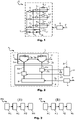
- the self-commutated cycloconverter 10 or also “matrix converter” has a switching matrix of converter valves S 11 to S 33 .
- the self-commutated cycloconverter 10 is a three-phase cycloconverter that converts three input phases U, V, and W into three output phases L1, L2, and L3.
- filter elements for vibration damping and buffering can be used between the respective input phases U, V and W, for example intermediate circuit capacitors C 12 , C 13 and C 23 .
- conventional filter elements for mains voltage filtering eg LC filters
- a three-phase motor can be connected to the three output phases L1, L2 and L3, so that the self-commutated cycloconverter 10 can be used together with the three-phase motor in an electrical drive system.
- a single-phase two-wire application can also be used, for example with a single-phase AC or DC machine as the load or with a single-phase network connected via an LC filter (e.g. as an island network or in parallel operation). In the latter case, one of the current-injected phases can remain free, i.e. not be connected to the two-wire application.
- converter valve S ij shows an exemplary configuration of one of the converter valves S 11 to S 33 (in 2 generally referred to as converter valve S ij ).
- the power converter valves S ij can have bidirectional switching elements 1, which can ensure current flow in both directions when switched on, but block current in both directions when switched off.
- bidirectional switching element 1 which have a bidirectional current flow (input current Ie and output current Io or vice versa) in the switched-on state and a bidirectional reverse blocking capability in the switched-off state.
- IGBT switches insulated gate electrodes
- Antiparallel diodes 3a and 3b can be connected across the respective IGBT switches 2a and 2b, respectively, which can either be implemented as separate components or can be integrated into the respective switch 2a or 2b.
- MOSFETs metal-oxide-semiconductor field-effect transistor switches
- IGBT switches 2a or 2b can be implemented, for example, based on silicon carbide (SiC MOSFETs).
- a bidirectional switching element can also be implemented as two anti-parallel connected thyristors, anti-parallel connected IGBTs with reverse blocking capability and switchable backwards or MOSFETs with reverse blocking capability and switchable backwards, each with a common gate connection or control connection. In these cases it may be necessary to provide a separate isolation circuit for each of the individual switches 2a or 2b.
- a converter control device 5 is provided for controlling the switches 2a, 2b of each of the converter valves S ij of the self-commutated cycloconverter 10, which generates pulse-width-modulated control signals X from analog setpoint signals P for the operation of the cycloconverter 10.
- a separate amplitude and phase-matched control signal X ij is generated for each of the power converter valves S ij of the cycloconverter 10 .
- the schematic block diagram of an exemplary power converter valve S ij of the self-commutated cycloconverter 10 of 2 1 also shows a valve control device 4 which is assigned to the respective bidirectional switching element 1.
- the valve control device 4 comprises, on the one hand, a commutation control device 6 and, on the other hand, two gate drivers 7a and 7b, one gate driver per switch 2a and 2b.
- 4-step commutation which inserts fixed delay times or dead times between the individual switching on and off processes of the switches of the bidirectional switching elements of a self-commutated cycloconverter in order to avoid load current interruptions and voltage peaks avoid.
- the valve control device 4 uses a state-dependent switch-on and switch-off delay, which can be dynamically adjusted based on a current amount of the load current.
- the commutation control device 6 is designed to receive the control signal X ij as an input signal from the converter control unit 5 and to use it to generate idealized gate signals for gate drivers 7a and 7b of the two switches 2a and 2b.
- the gate drivers 7a and 7b are in turn coupled to a delay control device 8 of the self-commutated cycloconverter 10, which receives instantaneous measured values for electrical operating parameters Z of the cycloconverter and, depending on the measured values obtained for the electrical operating parameters Z, transmits setpoint delay values Za or Eg calculated.
- the measured values for electrical operating parameters Z include, in particular, the direction of the load current flow and the magnitude of the instantaneous load current.
- the load currents in the respective converter branches can be measured and the deceleration setpoints Za or Zb can be formed on the one hand depending on the characteristics of the technology used of the switches 2a or 2b and on the other hand proportional to the instantaneous amount of the load current in the respective converter branch.
- the delay setpoints Za and Zb are fed to the gate drivers 7a and 7b, respectively, which generate delay-adapted gate signals Xa and Xb in dependence on the delay setpoints Za and Zb and the idealized gate signals received from the commutation controller 6.
- Delay matched gate signals Xa and Xb are used to drive the Switches 2a and 2b are applied to the respective gate terminals of switches 2a and 2b.
- the idealized gate signals Xa and Xb can be time-delayed such that it is on the current-impressing Page can come to no load current interruptions. At the same time branch short circuits on the voltage impressed side are avoided.
- 3(A) and (B) show schematic flowcharts of control methods MA and MB for a self-commutated cycloconverter.
- the control method MA and MB can, for example, for the control of the self-commutated cycloconverter 10 of 1 be used.
- the control method MA of 3(A) will be associated with 4 explained in more detail.
- 4 1 illustrates a timing diagram for drive signals of bidirectional switching elements, for example the bidirectional switching elements 1 of FIG 2 , to visualize the functioning of the control method MA of 3(A) .
- the activation method MA firstly comprises generating pulse-width-modulated control signals X ij for each of the converter valves S ij .
- the valve control device 4 of each of the converter valves S ij then generates idealized gate signals on the basis of the pulse-width-modulated control signal X ij for the respective converter valve S ij .
- load current-dependent setpoint deceleration values Za and Zb are determined in step M3, for example by a deceleration control device 8. These deceleration reference values are based on the measured instantaneous load current through the converter branches of the cycloconverter 10.
- step M4 the idealized gate signals are time-delayed as a function of the load-current-dependent setpoint delay values Za, Zb in order to form delay-adapted gate signals Xa, Xb, which can be applied to the gate connections of the switches 2a and 2b of the bidirectional switching element 1. How the delay-matched gate signals Xa, Xb can be formed in detail will be discussed in connection with FIG 4 explained below as an example.
- the signals shown are 2-bit signal curves over time for controlling switches, in which a switch is either switched on (signal value "1") or switched off (signal value "0").
- the signal curves each represent digital control signals for the gates of switches of bidirectional switching elements.
- the idealized control signals X1 and X2 for the theoretical ideal commutation of two back-to-back bidirectional switching elements 1 of different converter branches are shown in the top two signal curves marked as “base”. Up to a first point in time identified by the left dashed vertical line, the bidirectional switching element controlled by the control signal X2 is switched on, while the bidirectional switching element controlled by the control signal X1 is switched off. In the case of a theoretically ideal commutation, the switched-on bidirectional switching element would be switched off at exactly the same time as the switched-off bidirectional switching element is switched on. In the case of a further commutation at a second point in time identified by the dashed vertical line on the right, the process would then take place in reverse.
- the control signals X1 and X2 represent, for example, signal specifications according to a continuous pulse width modulation method.
- the commutation process is divided into four stages, between which locking periods are provided. Depending on requirements, the locking time periods can be dynamically adaptive or predetermined.
- the two following signal curve groups from the signal curves Xa1, Xb1, Xa2 and Xb2 each refer to cases of different load current directions in the converter branches - in the middle signal curve group the load current is positive (i>0), in the lower signal curve group the load current is negative (i ⁇ 0). It should be noted, however, that the properties "positive” and “negative” are only to be considered in relation to each other and are only used in the following explanations for the linguistically simpler differentiation of the two case groups.
- the current transfer occurs from the current-carrying converter branch "2", i.e. from the freewheeling diode 3b of the switch 2b, to the converter branch "1", i.e. to the switch 2a.
- the control signal Xb2 for the switch 2b of the current-carrying converter branch "2" is initially set to 0 in a first stage. Thereafter, a first branch locking period E1 is awaited before the control signal Xa1 for the switch 2a of the converter branch "1" which takes over the current is set to 1.
- a second branch locking time period is awaited, which corresponds to the time period T1+T2, before the control signal Xa2 for the switch 2a of the current-carrying converter branch "2" has been awaited. is set to 0.
- a third branch locking period E2 is then awaited before the control signal Xb1 for the switch 2a of the current-taking converter branch "1" is set to 1.
- the second branch locking time period between the switch-on edges of the two switches 2a and 2b of converter branch "1" thus defines the time period within which a minimum overlapping of the branch current flows can take place during the transition from one current-carrying converter branch to the next, so that during the commutation process even with real switch behavior and inductive commutation always on uninterrupted load current can flow. Therefore, the second arm lock period is set depending on the load current in the inverter arm "2". For example, the time spans T1 and T2 can be set dynamically in proportion to the magnitude of the load current.
- the periods of time T1 and T2 are mapped in the deceleration setpoint values Za and Zb generated by the deceleration control device 8 .
- deceleration is not meant exclusively as achievable by positive deceleration setpoints Za and Zb.
- the concept of delay should include both a negative and a positive time shift of signal edges.
- time periods T1 and T2 may be of the same length, in particular when the two switches 2a and 2b of the bidirectional switching element 1 are essentially of the same design and have similar characteristics. However, it can also be possible to choose the lengths of time T1 and T2 to be different.
- the first and third branch locking periods E1 and E2 can be set as constant based on characteristics of the switching elements, so that regardless of the direction of the current (i>0 or i ⁇ 0), branch locking is possible both with capacitive commutation and with commutation of a switch of the current-carrying converter branch to the freewheeling diode of the following Inverter branch is guaranteed. As a result, short circuits between the bridges on the voltage-impressed side ("mains side”) can be ruled out.
- the first and third branch locking periods E1 and E2 can be chosen to be of different lengths, depending on the polarity of the applied voltage and/or commutation stage.
- the branch locking times E1 and E2 ensure that, regardless of the direction of the load current, short circuits on the voltage-independent side of the cycloconverter can be ruled out, both with capacitive commutation and with commutation from a switch to the associated anti-parallel freewheeling diode of the downstream converter branch.
- the relative assignment of edges to each other is essential for the control of the cycloconverter. It follows from this that it can alternatively also be possible to use the continuous modulation signals before the output of a pulse width modulated signal with a positive or negative signal corresponding to the time to be delayed apply delay value. For example, in the case of a rising sawtooth signal in a continuous undershoot method, the continuous comparison or reference threshold value can be reduced by an amount corresponding to the time to be delayed, resulting in an edge that is earlier than the edge of an "idealized" signal. As a consequence, the same result of dynamically adapted branch locking time periods for the gate signals of the switching elements of the cycloconverter can be achieved by an adaptive delay of the pulse width modulated control signals.
- the control method MB of 3(B) therefore includes in step M3 a determination of load-current-dependent deceleration setpoints Za, Zb on the basis of the instantaneous load current through the converter branches of the cycloconverter 10. If in step M1 pulse-width-modulated control signals X ij have been generated for each of the converter valves S ij , these control signals X ij are then delayed in time in step M5 as a function of the load current-dependent deceleration setpoints Za, Zb to form delay-adapted control signals.
- gate signals for gate connections of the switches 2a, 2b of the bidirectional switching element 1 are then generated in the control method MB in step M6 by the valve control device 4 of each of the converter valves S ij .
- the dynamically adaptive delay setpoints in the adaptation of the gate signals make it possible advantageously to implement a continuous pulse width modulation method such as a space vector modulation, a sinusoidal pulse width modulation, a Schörner-Hanning pulse width modulation, a continuous undershoot method or a third harmonic injection method.
- a continuous pulse width modulation method such as a space vector modulation, a sinusoidal pulse width modulation, a Schörner-Hanning pulse width modulation, a continuous undershoot method or a third harmonic injection method.
- the delay to be adjusted depending on the state can be determined on the basis of the measured load currents in the converter branches and the theoretically ideal control signals of the continuous pulse width modulation can be delayed synchronously.
- figure 5 represents a general function block structure for the control of a self-commutated cycloconverter 10 with integrated valve control devices 4
- the converter control device 5 can have, for example, a calculation unit 5a for calculating analog phase and amplitude values V ij , which are modulated onto a carrier signal generated by a carrier frequency generator 9 in a comparator unit 5b.
- the carrier frequency generator 9 can generate descending sawtooth carrier signals, ascending sawtooth carrier signals or triangular carrier signals of the desired modulation frequency.
- the comparator unit 5b then outputs the control signals X ij for the individual valve control devices 4 integrated into the converter valves S ij of the self-commutated cycloconverter 10, which in turn are divided into two gate signals Xa and Xb, taking into account the deceleration setpoint values generated by the deceleration control device 8.
- the deceleration control device 8 can, in particular, receive the measured values of the electrical operating parameters Z required for determining the deceleration setpoint values from a load current measuring device 8a of the cycloconverter 10 .
- the integrated valve control devices 4 can each be implemented on a field programmable gate array (FPGA) or an application-specific integrated circuit (ASIC), for example.
- the self-commutated cycloconverters described above can advantageously implement a bidirectional current flow from the network to the load side and vice versa.
- Self-commutated cycloconverters offer the possibility of adjusting a power factor and improving the quality of the waveforms.
- Self-commutated cycloconverters also have a compact and cost-efficient design and offer good electromagnetic compatibility. Based on their specific properties, in addition to the possible uses for motor control, there are also application options as step-down converters and within combined circuit architectures for energy supply capable of peak loads.
Landscapes
- Engineering & Computer Science (AREA)
- Power Engineering (AREA)
- Ac-Ac Conversion (AREA)
Claims (9)
- Convertisseur direct à commutation automatique (10), comprenant :une matrice de commutation composée de plusieurs valves de convertisseur (Sij) qui présentent chacune un élément de commutation bidirectionnel (1) présentant deux commutateurs (2a, 2b),caractérisé en ce que les valves de convertisseur (Sij) présentent chacune un moyen de commande de valve (4), les moyens de commande de valve (4) présentant chacun :un dispositif de commande de commutation (6) qui est conçu pour recevoir des signaux de commande modulés en largeur d'impulsion (Xij) et pour générer des signaux de grille idéalisés sur la base de ceux-ci ; etdeux pilotes de grille (7a ; 7b) qui sont couplés au dispositif de commande de commutation (6) et qui sont conçus pour décaler dans le temps, en fonction de valeurs de consigne de retard négatives ou positives (Za ; Zb) dépendantes du courant de charge, les signaux de grille idéalisés reçus par le dispositif de commande de commutation (6) et pour les délivrer en tant que signaux de grille (Xa ; Xb) adaptés au retard à des connexions de grille des commutateurs (2a ; 2b) de l'élément de commutation bidirectionnel (1) .
- Convertisseur direct (10) selon la revendication 1, dans lequel les signaux de commande modulés en largeur d'impulsion (Xij) sont générés sur la base d'un procédé de modulation de largeur d'impulsion continue.
- Convertisseur direct (10) selon la revendication 2, dans lequel le procédé de modulation de largeur d'impulsion continue comprend un procédé de modulation par vecteur spatial ou un procédé de sous-oscillation continue.
- Convertisseur direct (10) selon l'une des revendications 1 à 3, présentant en outre :
un moyen de commande de retard (8) couplé aux pilotes de grille (7a, 7b), qui reçoit des valeurs de mesure instantanées de paramètres de fonctionnement électriques (Z) du convertisseur direct (10) et calcule les valeurs de consigne de retard (Za ; Zb) dépendantes du courant de charge en fonction des valeurs de mesure instantanées des paramètres de fonctionnement électriques (Z). - Convertisseur direct (10) selon la revendication 4, dans lequel les valeurs de mesure instantanées des paramètres de fonctionnement électriques (Z) comprennent la direction du flux de courant de charge et le montant du courant de charge instantané dans les différentes branches de convertisseur du convertisseur direct (10).
- Convertisseur direct (10) selon l'une des revendications 1 à 5, dans lequel les commutateurs (2a ; 2b) de l'élément de commutation bidirectionnel comprennent des commutateurs à semi-conducteurs montés en anti-série avec des diodes de roue libre (3a ; 3b) montées chaque fois en antiparallèle.
- Convertisseur direct (10) selon la revendication 6, dans lequel les commutateurs à semi-conducteurs montés en anti-série comprennent des commutateurs IGBT ou des commutateurs MOSFET, en particulier des commutateurs MOSFET SiC.
- Procédé de commande (MA) pour un convertisseur direct à commutation automatique (10) comprenant une matrice de commutation composée de plusieurs valves de convertisseur (Sij) qui présentent chacune un élément de commutation bidirectionnel (1) présentant deux commutateurs (2a, 2b) et un moyen de commande de valve (4), caractérisé en ce que le procédé de commande (M) comprend les étapes consistant à :générer (M1) des signaux de commande modulés en largeur d'impulsion (Xij) pour chacune des valves de convertisseur (Sij) ;générer (M2), par le moyen de commande de valve (4) de chacune des valves de convertisseur (Sij), des signaux de grille idéalisés sur la base du signal de commande modulé en largeur d'impulsion (Xij) pour la valve de convertisseur respective (Sij) ;déterminer (M3) des valeurs de consigne de retard négatives ou positives dépendantes du courant de charge (Za ; Zb) sur la base du courant de charge instantané à travers les branches de convertisseur du convertisseur direct (10) ; etdécaler dans le temps (M4) les signaux de grille idéalisés en fonction des valeurs de consigne de retard dépendantes du courant de charge (Za ; Zb) pour former des signaux de grille adaptés au retard (Xa ; Xb) pour des connexions de grille des commutateurs (2a ; 2b) de l'élément de commutation bidirectionnel (1).
- Système d'entraînement électrique, comprenant :un convertisseur direct à commutation automatique (10) selon l'une des revendications 1 à 7 ;une machine électrique connectée aux phases de sortie (L1 ; L2 ; L3) ; etun filtre de tension réseau qui est couplé aux phases d'entrée (U ; V ; W) du convertisseur direct à commutation automatique (10).
Applications Claiming Priority (1)
| Application Number | Priority Date | Filing Date | Title |
|---|---|---|---|
| DE102018006120.6A DE102018006120A1 (de) | 2018-08-02 | 2018-08-02 | Selbstgeführter Direktumrichter und Ansteuerverfahren für selbstgeführten Direktumrichter |
Publications (2)
| Publication Number | Publication Date |
|---|---|
| EP3605821A1 EP3605821A1 (fr) | 2020-02-05 |
| EP3605821B1 true EP3605821B1 (fr) | 2022-05-18 |
Family
ID=66776198
Family Applications (1)
| Application Number | Title | Priority Date | Filing Date |
|---|---|---|---|
| EP19178714.2A Active EP3605821B1 (fr) | 2018-08-02 | 2019-06-06 | Onduleur direct autoguidé et procédé de commande pour l'onduleur direct autoguidé |
Country Status (2)
| Country | Link |
|---|---|
| EP (1) | EP3605821B1 (fr) |
| DE (1) | DE102018006120A1 (fr) |
Families Citing this family (3)
| Publication number | Priority date | Publication date | Assignee | Title |
|---|---|---|---|---|
| GB2591768B (en) * | 2020-02-05 | 2023-01-04 | Sprint Electric Ltd | Bidirectional switch control |
| CN112202355B (zh) * | 2020-09-09 | 2024-03-15 | 惠州志顺电子实业有限公司 | 逆变器控制方法、控制装置、逆变器装置以及存储介质 |
| US20250260254A1 (en) * | 2024-02-14 | 2025-08-14 | Qualcomm Incorporated | Power supply circuit having back-to-back transistors with separate gate control and/or separate current sensing |
Family Cites Families (4)
| Publication number | Priority date | Publication date | Assignee | Title |
|---|---|---|---|---|
| US5892677A (en) * | 1997-06-02 | 1999-04-06 | Reliance Electric Industrial Company | Adaptive overlapping communication control of modular AC-AC converter and integration with device module of multiple AC-AC switches |
| DE10057785A1 (de) * | 2000-11-22 | 2002-06-06 | Siemens Ag | Verfahren zur Steuerung eines Matrixumrichters |
| GB0208600D0 (en) * | 2002-04-15 | 2002-05-22 | Nottingham University | Power converter |
| JP5839014B2 (ja) * | 2013-09-26 | 2016-01-06 | 株式会社安川電機 | マトリクスコンバータ |
-
2018
- 2018-08-02 DE DE102018006120.6A patent/DE102018006120A1/de active Pending
-
2019
- 2019-06-06 EP EP19178714.2A patent/EP3605821B1/fr active Active
Also Published As
| Publication number | Publication date |
|---|---|
| EP3605821A1 (fr) | 2020-02-05 |
| DE102018006120A1 (de) | 2020-02-06 |
Similar Documents
| Publication | Publication Date | Title |
|---|---|---|
| EP2537239B1 (fr) | Onduleur à découpage à 3 étages avec réseau de délestage | |
| EP2737618B1 (fr) | Système de convertisseur électrique | |
| EP0660498B1 (fr) | Dispositif et méthode pour la transformation de courant alternatif triphasé en courant continu | |
| DE112008001796B4 (de) | Wechselrichtersystem und Steuerverfahren | |
| WO2007115893A1 (fr) | Onduleur à faible encombrement avec pertes de commutation réduites et durée de vie accrue | |
| EP3211784A1 (fr) | Sous-module double pour un convertisseur de frequence multipoints modulaire et convertisseur de frequence multipoints modulaire en etant dote | |
| EP2709257A2 (fr) | Circuit de convertisseur de courant et procédé de commande du circuit de convertisseur de courant | |
| EP3605821B1 (fr) | Onduleur direct autoguidé et procédé de commande pour l'onduleur direct autoguidé | |
| WO2012122978A2 (fr) | Convertisseur pour un moteur électrique et procédé de commande d'un disjoncteur | |
| EP2992595A1 (fr) | Ensemble mutateur à mutateurs multi-étages câblés en parallèle et son procédé de commande | |
| DE102017115639A1 (de) | Reduzierung des Rippelstroms bei Schaltvorgängen einer Brückenschaltung | |
| WO2009156021A1 (fr) | Circuit transformateur de tension et onduleur | |
| EP2741934A1 (fr) | Procédé et circuit pour le fonctionnement multiphasé d'un moteur électrique | |
| DE102004023299B4 (de) | Steuerverfahren und Schaltungsanordnung für einen Gleichrichter | |
| EP2732544A1 (fr) | Procédé de régulation d'une tension au point milieu | |
| EP1137160B1 (fr) | Circuit convertisseur de puissance | |
| EP3095178A1 (fr) | Convertisseur de puissance modulaire comprenant des sous-modules, lesquels fonctionnent en mode linéaire | |
| WO2010088979A1 (fr) | Procédé de régulation d'un convertisseur côté réseau à commutation automatique dans un convertisseur indirect de tension | |
| DE102007040166B4 (de) | Motorsteuerungsvorrichtung | |
| EP2928055B1 (fr) | Convertisseur de courant modulaire et procédé de production d'une tension de sortie sinusoïdale à harmoniques réduites | |
| EP4545348A1 (fr) | Réseau de traction pour un véhicule automobile | |
| DE102013215992A1 (de) | Dreiphasige Mehrpunkt-Stromrichteranordnung als AC/AC-Umrichter | |
| WO2013023981A1 (fr) | Procédé et dispositif de commande d'un circuit convertisseur | |
| DE10246526B4 (de) | Verfahren zur Ansteuerung eines Matrixumrichters | |
| WO2016092091A1 (fr) | Élément multiple pour convertisseurs à base d'éléments |
Legal Events
| Date | Code | Title | Description |
|---|---|---|---|
| PUAI | Public reference made under article 153(3) epc to a published international application that has entered the european phase |
Free format text: ORIGINAL CODE: 0009012 |
|
| STAA | Information on the status of an ep patent application or granted ep patent |
Free format text: STATUS: THE APPLICATION HAS BEEN PUBLISHED |
|
| AK | Designated contracting states |
Kind code of ref document: A1 Designated state(s): AL AT BE BG CH CY CZ DE DK EE ES FI FR GB GR HR HU IE IS IT LI LT LU LV MC MK MT NL NO PL PT RO RS SE SI SK SM TR |
|
| AX | Request for extension of the european patent |
Extension state: BA ME |
|
| STAA | Information on the status of an ep patent application or granted ep patent |
Free format text: STATUS: REQUEST FOR EXAMINATION WAS MADE |
|
| 17P | Request for examination filed |
Effective date: 20200421 |
|
| RBV | Designated contracting states (corrected) |
Designated state(s): AL AT BE BG CH CY CZ DE DK EE ES FI FR GB GR HR HU IE IS IT LI LT LU LV MC MK MT NL NO PL PT RO RS SE SI SK SM TR |
|
| GRAP | Despatch of communication of intention to grant a patent |
Free format text: ORIGINAL CODE: EPIDOSNIGR1 |
|
| STAA | Information on the status of an ep patent application or granted ep patent |
Free format text: STATUS: GRANT OF PATENT IS INTENDED |
|
| INTG | Intention to grant announced |
Effective date: 20220110 |
|
| GRAS | Grant fee paid |
Free format text: ORIGINAL CODE: EPIDOSNIGR3 |
|
| GRAA | (expected) grant |
Free format text: ORIGINAL CODE: 0009210 |
|
| STAA | Information on the status of an ep patent application or granted ep patent |
Free format text: STATUS: THE PATENT HAS BEEN GRANTED |
|
| AK | Designated contracting states |
Kind code of ref document: B1 Designated state(s): AL AT BE BG CH CY CZ DE DK EE ES FI FR GB GR HR HU IE IS IT LI LT LU LV MC MK MT NL NO PL PT RO RS SE SI SK SM TR |
|
| REG | Reference to a national code |
Ref country code: GB Ref legal event code: FG4D Free format text: NOT ENGLISH |
|
| REG | Reference to a national code |
Ref country code: CH Ref legal event code: EP |
|
| REG | Reference to a national code |
Ref country code: IE Ref legal event code: FG4D Free format text: LANGUAGE OF EP DOCUMENT: GERMAN |
|
| REG | Reference to a national code |
Ref country code: DE Ref legal event code: R096 Ref document number: 502019004394 Country of ref document: DE |
|
| REG | Reference to a national code |
Ref country code: AT Ref legal event code: REF Ref document number: 1493716 Country of ref document: AT Kind code of ref document: T Effective date: 20220615 |
|
| REG | Reference to a national code |
Ref country code: LT Ref legal event code: MG9D |
|
| REG | Reference to a national code |
Ref country code: NL Ref legal event code: MP Effective date: 20220518 |
|
| PG25 | Lapsed in a contracting state [announced via postgrant information from national office to epo] |
Ref country code: SE Free format text: LAPSE BECAUSE OF FAILURE TO SUBMIT A TRANSLATION OF THE DESCRIPTION OR TO PAY THE FEE WITHIN THE PRESCRIBED TIME-LIMIT Effective date: 20220518 Ref country code: PT Free format text: LAPSE BECAUSE OF FAILURE TO SUBMIT A TRANSLATION OF THE DESCRIPTION OR TO PAY THE FEE WITHIN THE PRESCRIBED TIME-LIMIT Effective date: 20220919 Ref country code: NO Free format text: LAPSE BECAUSE OF FAILURE TO SUBMIT A TRANSLATION OF THE DESCRIPTION OR TO PAY THE FEE WITHIN THE PRESCRIBED TIME-LIMIT Effective date: 20220818 Ref country code: NL Free format text: LAPSE BECAUSE OF FAILURE TO SUBMIT A TRANSLATION OF THE DESCRIPTION OR TO PAY THE FEE WITHIN THE PRESCRIBED TIME-LIMIT Effective date: 20220518 Ref country code: LT Free format text: LAPSE BECAUSE OF FAILURE TO SUBMIT A TRANSLATION OF THE DESCRIPTION OR TO PAY THE FEE WITHIN THE PRESCRIBED TIME-LIMIT Effective date: 20220518 Ref country code: HR Free format text: LAPSE BECAUSE OF FAILURE TO SUBMIT A TRANSLATION OF THE DESCRIPTION OR TO PAY THE FEE WITHIN THE PRESCRIBED TIME-LIMIT Effective date: 20220518 Ref country code: GR Free format text: LAPSE BECAUSE OF FAILURE TO SUBMIT A TRANSLATION OF THE DESCRIPTION OR TO PAY THE FEE WITHIN THE PRESCRIBED TIME-LIMIT Effective date: 20220819 Ref country code: FI Free format text: LAPSE BECAUSE OF FAILURE TO SUBMIT A TRANSLATION OF THE DESCRIPTION OR TO PAY THE FEE WITHIN THE PRESCRIBED TIME-LIMIT Effective date: 20220518 Ref country code: ES Free format text: LAPSE BECAUSE OF FAILURE TO SUBMIT A TRANSLATION OF THE DESCRIPTION OR TO PAY THE FEE WITHIN THE PRESCRIBED TIME-LIMIT Effective date: 20220518 Ref country code: BG Free format text: LAPSE BECAUSE OF FAILURE TO SUBMIT A TRANSLATION OF THE DESCRIPTION OR TO PAY THE FEE WITHIN THE PRESCRIBED TIME-LIMIT Effective date: 20220818 |
|
| PG25 | Lapsed in a contracting state [announced via postgrant information from national office to epo] |
Ref country code: RS Free format text: LAPSE BECAUSE OF FAILURE TO SUBMIT A TRANSLATION OF THE DESCRIPTION OR TO PAY THE FEE WITHIN THE PRESCRIBED TIME-LIMIT Effective date: 20220518 Ref country code: PL Free format text: LAPSE BECAUSE OF FAILURE TO SUBMIT A TRANSLATION OF THE DESCRIPTION OR TO PAY THE FEE WITHIN THE PRESCRIBED TIME-LIMIT Effective date: 20220518 Ref country code: LV Free format text: LAPSE BECAUSE OF FAILURE TO SUBMIT A TRANSLATION OF THE DESCRIPTION OR TO PAY THE FEE WITHIN THE PRESCRIBED TIME-LIMIT Effective date: 20220518 Ref country code: IS Free format text: LAPSE BECAUSE OF FAILURE TO SUBMIT A TRANSLATION OF THE DESCRIPTION OR TO PAY THE FEE WITHIN THE PRESCRIBED TIME-LIMIT Effective date: 20220918 |
|
| PG25 | Lapsed in a contracting state [announced via postgrant information from national office to epo] |
Ref country code: SM Free format text: LAPSE BECAUSE OF FAILURE TO SUBMIT A TRANSLATION OF THE DESCRIPTION OR TO PAY THE FEE WITHIN THE PRESCRIBED TIME-LIMIT Effective date: 20220518 Ref country code: SK Free format text: LAPSE BECAUSE OF FAILURE TO SUBMIT A TRANSLATION OF THE DESCRIPTION OR TO PAY THE FEE WITHIN THE PRESCRIBED TIME-LIMIT Effective date: 20220518 Ref country code: RO Free format text: LAPSE BECAUSE OF FAILURE TO SUBMIT A TRANSLATION OF THE DESCRIPTION OR TO PAY THE FEE WITHIN THE PRESCRIBED TIME-LIMIT Effective date: 20220518 Ref country code: EE Free format text: LAPSE BECAUSE OF FAILURE TO SUBMIT A TRANSLATION OF THE DESCRIPTION OR TO PAY THE FEE WITHIN THE PRESCRIBED TIME-LIMIT Effective date: 20220518 Ref country code: DK Free format text: LAPSE BECAUSE OF FAILURE TO SUBMIT A TRANSLATION OF THE DESCRIPTION OR TO PAY THE FEE WITHIN THE PRESCRIBED TIME-LIMIT Effective date: 20220518 Ref country code: CZ Free format text: LAPSE BECAUSE OF FAILURE TO SUBMIT A TRANSLATION OF THE DESCRIPTION OR TO PAY THE FEE WITHIN THE PRESCRIBED TIME-LIMIT Effective date: 20220518 |
|
| REG | Reference to a national code |
Ref country code: CH Ref legal event code: PL |
|
| REG | Reference to a national code |
Ref country code: BE Ref legal event code: MM Effective date: 20220630 |
|
| REG | Reference to a national code |
Ref country code: DE Ref legal event code: R097 Ref document number: 502019004394 Country of ref document: DE |
|
| PG25 | Lapsed in a contracting state [announced via postgrant information from national office to epo] |
Ref country code: MC Free format text: LAPSE BECAUSE OF FAILURE TO SUBMIT A TRANSLATION OF THE DESCRIPTION OR TO PAY THE FEE WITHIN THE PRESCRIBED TIME-LIMIT Effective date: 20220518 |
|
| PLBE | No opposition filed within time limit |
Free format text: ORIGINAL CODE: 0009261 |
|
| STAA | Information on the status of an ep patent application or granted ep patent |
Free format text: STATUS: NO OPPOSITION FILED WITHIN TIME LIMIT |
|
| PG25 | Lapsed in a contracting state [announced via postgrant information from national office to epo] |
Ref country code: AL Free format text: LAPSE BECAUSE OF FAILURE TO SUBMIT A TRANSLATION OF THE DESCRIPTION OR TO PAY THE FEE WITHIN THE PRESCRIBED TIME-LIMIT Effective date: 20220518 |
|
| 26N | No opposition filed |
Effective date: 20230221 |
|
| PG25 | Lapsed in a contracting state [announced via postgrant information from national office to epo] |
Ref country code: LU Free format text: LAPSE BECAUSE OF NON-PAYMENT OF DUE FEES Effective date: 20220606 Ref country code: LI Free format text: LAPSE BECAUSE OF NON-PAYMENT OF DUE FEES Effective date: 20220630 Ref country code: IE Free format text: LAPSE BECAUSE OF NON-PAYMENT OF DUE FEES Effective date: 20220606 Ref country code: FR Free format text: LAPSE BECAUSE OF NON-PAYMENT OF DUE FEES Effective date: 20220718 Ref country code: CH Free format text: LAPSE BECAUSE OF NON-PAYMENT OF DUE FEES Effective date: 20220630 |
|
| PG25 | Lapsed in a contracting state [announced via postgrant information from national office to epo] |
Ref country code: SI Free format text: LAPSE BECAUSE OF FAILURE TO SUBMIT A TRANSLATION OF THE DESCRIPTION OR TO PAY THE FEE WITHIN THE PRESCRIBED TIME-LIMIT Effective date: 20220518 Ref country code: BE Free format text: LAPSE BECAUSE OF NON-PAYMENT OF DUE FEES Effective date: 20220630 |
|
| P01 | Opt-out of the competence of the unified patent court (upc) registered |
Effective date: 20230510 |
|
| PG25 | Lapsed in a contracting state [announced via postgrant information from national office to epo] |
Ref country code: IT Free format text: LAPSE BECAUSE OF FAILURE TO SUBMIT A TRANSLATION OF THE DESCRIPTION OR TO PAY THE FEE WITHIN THE PRESCRIBED TIME-LIMIT Effective date: 20220518 |
|
| GBPC | Gb: european patent ceased through non-payment of renewal fee |
Effective date: 20230606 |
|
| PG25 | Lapsed in a contracting state [announced via postgrant information from national office to epo] |
Ref country code: MK Free format text: LAPSE BECAUSE OF FAILURE TO SUBMIT A TRANSLATION OF THE DESCRIPTION OR TO PAY THE FEE WITHIN THE PRESCRIBED TIME-LIMIT Effective date: 20220511 Ref country code: CY Free format text: LAPSE BECAUSE OF FAILURE TO SUBMIT A TRANSLATION OF THE DESCRIPTION OR TO PAY THE FEE WITHIN THE PRESCRIBED TIME-LIMIT Effective date: 20220511 Ref country code: GB Free format text: LAPSE BECAUSE OF NON-PAYMENT OF DUE FEES Effective date: 20230606 |
|
| PG25 | Lapsed in a contracting state [announced via postgrant information from national office to epo] |
Ref country code: HU Free format text: LAPSE BECAUSE OF FAILURE TO SUBMIT A TRANSLATION OF THE DESCRIPTION OR TO PAY THE FEE WITHIN THE PRESCRIBED TIME-LIMIT; INVALID AB INITIO Effective date: 20190606 |
|
| PG25 | Lapsed in a contracting state [announced via postgrant information from national office to epo] |
Ref country code: MT Free format text: LAPSE BECAUSE OF FAILURE TO SUBMIT A TRANSLATION OF THE DESCRIPTION OR TO PAY THE FEE WITHIN THE PRESCRIBED TIME-LIMIT Effective date: 20220511 |
|
| PG25 | Lapsed in a contracting state [announced via postgrant information from national office to epo] |
Ref country code: BG Free format text: LAPSE BECAUSE OF FAILURE TO SUBMIT A TRANSLATION OF THE DESCRIPTION OR TO PAY THE FEE WITHIN THE PRESCRIBED TIME-LIMIT Effective date: 20220518 |
|
| PG25 | Lapsed in a contracting state [announced via postgrant information from national office to epo] |
Ref country code: BG Free format text: LAPSE BECAUSE OF FAILURE TO SUBMIT A TRANSLATION OF THE DESCRIPTION OR TO PAY THE FEE WITHIN THE PRESCRIBED TIME-LIMIT Effective date: 20220518 |
|
| REG | Reference to a national code |
Ref country code: AT Ref legal event code: MM01 Ref document number: 1493716 Country of ref document: AT Kind code of ref document: T Effective date: 20240606 |
|
| PGFP | Annual fee paid to national office [announced via postgrant information from national office to epo] |
Ref country code: DE Payment date: 20250630 Year of fee payment: 7 |
|
| PG25 | Lapsed in a contracting state [announced via postgrant information from national office to epo] |
Ref country code: AT Free format text: LAPSE BECAUSE OF NON-PAYMENT OF DUE FEES Effective date: 20240606 |
|
| PG25 | Lapsed in a contracting state [announced via postgrant information from national office to epo] |
Ref country code: TR Free format text: LAPSE BECAUSE OF FAILURE TO SUBMIT A TRANSLATION OF THE DESCRIPTION OR TO PAY THE FEE WITHIN THE PRESCRIBED TIME-LIMIT Effective date: 20220518 |
|
| PGFP | Annual fee paid to national office [announced via postgrant information from national office to epo] |
Ref country code: AT Payment date: 20260410 Year of fee payment: 5 |