EP3607619B1 - Système de connecteur enfichable - Google Patents
Système de connecteur enfichable Download PDFInfo
- Publication number
- EP3607619B1 EP3607619B1 EP18716207.8A EP18716207A EP3607619B1 EP 3607619 B1 EP3607619 B1 EP 3607619B1 EP 18716207 A EP18716207 A EP 18716207A EP 3607619 B1 EP3607619 B1 EP 3607619B1
- Authority
- EP
- European Patent Office
- Prior art keywords
- connector
- electrical
- plug
- contact
- circuit board
- Prior art date
- Legal status (The legal status is an assumption and is not a legal conclusion. Google has not performed a legal analysis and makes no representation as to the accuracy of the status listed.)
- Active
Links
Images


Classifications
-
- H—ELECTRICITY
- H01—ELECTRIC ELEMENTS
- H01R—ELECTRICALLY-CONDUCTIVE CONNECTIONS; STRUCTURAL ASSOCIATIONS OF A PLURALITY OF MUTUALLY-INSULATED ELECTRICAL CONNECTING ELEMENTS; COUPLING DEVICES; CURRENT COLLECTORS
- H01R13/00—Details of coupling devices of the kinds covered by groups H01R12/70 or H01R24/00 - H01R33/00
- H01R13/66—Structural association with built-in electrical component
- H01R13/665—Structural association with built-in electrical component with built-in electronic circuit
- H01R13/6658—Structural association with built-in electrical component with built-in electronic circuit on printed circuit board
-
- H—ELECTRICITY
- H01—ELECTRIC ELEMENTS
- H01R—ELECTRICALLY-CONDUCTIVE CONNECTIONS; STRUCTURAL ASSOCIATIONS OF A PLURALITY OF MUTUALLY-INSULATED ELECTRICAL CONNECTING ELEMENTS; COUPLING DEVICES; CURRENT COLLECTORS
- H01R13/00—Details of coupling devices of the kinds covered by groups H01R12/70 or H01R24/00 - H01R33/00
- H01R13/648—Protective earth or shield arrangements on coupling devices, e.g. anti-static shielding
- H01R13/658—High frequency shielding arrangements, e.g. against EMI [Electro-Magnetic Interference] or EMP [Electro-Magnetic Pulse]
- H01R13/6581—Shield structure
-
- H—ELECTRICITY
- H01—ELECTRIC ELEMENTS
- H01R—ELECTRICALLY-CONDUCTIVE CONNECTIONS; STRUCTURAL ASSOCIATIONS OF A PLURALITY OF MUTUALLY-INSULATED ELECTRICAL CONNECTING ELEMENTS; COUPLING DEVICES; CURRENT COLLECTORS
- H01R29/00—Coupling parts for selective co-operation with a counterpart in different ways to establish different circuits, e.g. for voltage selection, for series-parallel selection, programmable connectors
-
- H—ELECTRICITY
- H01—ELECTRIC ELEMENTS
- H01R—ELECTRICALLY-CONDUCTIVE CONNECTIONS; STRUCTURAL ASSOCIATIONS OF A PLURALITY OF MUTUALLY-INSULATED ELECTRICAL CONNECTING ELEMENTS; COUPLING DEVICES; CURRENT COLLECTORS
- H01R13/00—Details of coupling devices of the kinds covered by groups H01R12/70 or H01R24/00 - H01R33/00
- H01R13/648—Protective earth or shield arrangements on coupling devices, e.g. anti-static shielding
- H01R13/658—High frequency shielding arrangements, e.g. against EMI [Electro-Magnetic Interference] or EMP [Electro-Magnetic Pulse]
- H01R13/6591—Specific features or arrangements of connection of shield to conductive members
- H01R13/65912—Specific features or arrangements of connection of shield to conductive members for shielded multiconductor cable
Definitions
- the invention relates to a connector system having an electrical connector for connection to at least one electrical line and an electrical circuit.
- Plug connectors for separating and connecting lines are well known and are used in various forms, especially in electrical engineering.
- a connector can be a plug, a socket, a coupling or an adapter.
- the plug connector can be used to connect to at least one cable and / or to at least one printed circuit board (also called “printed circuit board”, PCB).
- PCB printed circuit board
- cables can be replaced quickly and easily, in contrast to other system components.
- Such an exchange can be necessary for many reasons, for example because of damage or a system change or system expansion.
- cables laid in a motor vehicle are usually only in partial areas, e.g. B. in the area of connectors, accessible without major disassembly effort.
- the object of the present invention is to provide an improved connector system in which the interconnection can be adapted even more easily than with the current state of the art.
- the connector system according to the invention has an electrical connector for connection to at least one electrical line and an electrical circuit.
- the electrical circuit preferably has at least one electrical component.
- An electrical line is to be understood as any device for transporting or transmitting electrical energy for data transmission and / or for electrical supply.
- the electrical line is preferably an electrical cable consisting of a combination of several individual lines.
- An electrical cable generally has a ground conductor or outer conductor and one or more signal conductors in the form of inner conductors.
- the electrical line is an electrical line of an electrical device, a further plug connector or an electrical line on a circuit board, for example a microstrip line or a connection point to a microstrip line.
- ground conductor can be understood to mean any electrical conductor that carries a ground potential or some other reference potential.
- signal conductor can be understood to mean any conductor for the transmission of electrical data signals and / or electrical supply signals.
- the plug connector can preferably have a housing for receiving the at least one electrical line, for example for receiving an electrical cable.
- a single cable can be received by the housing.
- it can be advantageous to provide means for sealing and / or for intercepting forces that act on the cable, which are well known from the prior art.
- the housing can be an electrically conductive housing, for example consisting of a metal, or preferably an electrically non-conductive housing, for example consisting of a plastic.
- a mixed form is also possible.
- the use of a plastic housing is usually simpler in terms of production technology and, depending on the place of use, can also offer advantages from an electrical engineering point of view due to the insulating properties.
- the electrical connector further comprises at least one input-side contact that can be connected to a signal conductor of the electrical line (e.g. a cable inner conductor of an electrical cable), and at least one output-side contact that can be electrically connected to a connector inner conductor.
- a signal conductor of the electrical line e.g. a cable inner conductor of an electrical cable
- the input-side contact of the connector to which the electrical conductor is connected or at which the at least one cable with the at least one inner conductor is received and the output-side contact of the connector are therefore fundamentally, i.e. without further measures and configurations described below, not electrically connected to each other.
- the at least one input-side contact and the at least one output-side contact are spatially separated from one another.
- the two contacts can be opposite, i. H. be arranged in a line or axis.
- the mutually facing ends of the input-side contacts and the output-side contacts are arranged in two mutually opposite, preferably parallel, planes.
- a single-pole connector or a multi-pole connector is used. That is to say, provision can be made to provide one input-side contact and one output-side contact or more than one input-side contact and more than one output-side contact.
- two to twenty input-side contacts particularly preferably three to ten input-side contacts and very particularly preferably up to four input-side contacts, are provided in each case.
- the number of contacts on the output side is preferably designed analogously.
- the number of signal conductors or cable inner conductors and input-side contacts or the number of plug-in connector inner conductors and output-side contacts can also differ. It can e.g. B. several signal conductors or cable inner conductors are brought together on the same input-side contact.
- the electrical connector also has means for shielding, which can be electrically connected to a ground conductor of the at least one electrical line (for example an outer conductor of the at least one cable).
- the plug connector has a receptacle for the electrical circuit and a closure element for closing an access opening of the receptacle.
- the receptacle is preferably arranged in such a way that it spatially separates or separates the at least one input-side contact and the at least one output-side contact is located between the at least one input-side contact and the at least one output-side contact.
- the electrical circuit has contact points in order to contact at least one input-side contact and at least one output-side contact when the electrical circuit is inserted into the receptacle. Furthermore, the electrical circuit has a transmission option from the at least one input-side contact to the at least one output-side contact.
- the transmission options can be designed individually for each line or for each signal conductor or for each contact or for each signal to be transmitted.
- the electrical circuit can be inserted between the at least one input-side contact and the at least one output-side contact that a contact point or contact points of an input-side contact surface of the electrical circuit contact the at least one input-side contact and a contact point or contact points of a contact surface of the electrical circuit on the output side (which preferably runs parallel to the contact surface on the input side and is oriented in the opposite direction) contact the at least one contact on the output side.
- the electrical circuit as a circuit board, preferably as a two-sided circuit board (with two circuit board layers) or as a multi-layer circuit board with more than two circuit board layers, as a multi-chip module, as a system-in-package, as System-on-chip and / or is designed as an integrated circuit.
- the electrical circuit can be designed as a printed circuit board with one or more printed circuit board layers.
- microchips can also be provided for the formation of the electrical circuit to arrange several microchips in the manner of a so-called "multi-chip module” one above the other and / or next to one another in a common chip housing ("package"), the microchips within the chip Housing among each other and / or are connected to the contact points of the chip housing or the electrical circuit via so-called bond wires - or by some other known connection technology.
- the electrical circuit can also be designed as a "system-in-package", wherein one or more microchips are arranged together with at least one further electrical component (e.g. together with coupling capacitors) within a common chip housing and are connected by bonding wires (or in any other way) are connected to one another and / or to the contact points of the electrical circuit.
- a further electrical component e.g. together with coupling capacitors
- a so-called "system-on-chip” or a conventional microchip or a single application-specific integrated circuit can also be provided in a chip housing with contact points arranged on the chip housing in order to implement the electrical circuit.
- the electrical circuit in particular a multilayer printed circuit board, can preferably have a metallization on at least one surface, preferably on all surfaces facing outwards.
- the connector system according to the invention enables the use of a modular connector which, by inserting a specific electrical circuit, eg. B. a circuit board with a desired electronics, for example, shows signal-improving properties.
- the functions of the connector can thus be defined by various types of electrical circuits.
- the connector and the electrical line connected to the connector can be produced in an identical manner for a large number of applications. Only the electrical circuits have to be individually adapted to the specific application variant. Furthermore, the installation or assembly of the electrical circuit is easily possible. In this way, an end user could even decide on the variant to be installed or simply change the variant, for example an expansion of functions.
- the electrical circuit that can be inserted into the receptacle is only used once by the manufacturer, thereby defining the functionality of the connector or the cable connected to it.
- the connector system described can be used particularly advantageously in the automotive sector. Components can be modified quickly and inexpensively without having to intervene in the adjacent electronics or replacing an entire cable, circuit board and / or device, e.g. B. a control unit would be required.
- the connector system according to the invention can also be used in the manner of an adapter or adapter plug.
- the electrical circuit can be used as an activation module for extended functions that can be purchased, for example, by an end user.
- the connector system can thus be used to form an access authorization system.
- the electrical circuit when it is inserted into the receptacle, is positioned between the at least one input-side contact and the at least one output-side contact.
- the contacts and / or contact points can (each) all be implemented with the same type of contact or with different types of contact. Any combination is possible.
- the contact points of the electrical circuit and / or the contacts of the connector are flat contacts and / or sliding contacts and / or soldering surfaces (also called “pads") and / or spring contacts (e.g. pogo pins ) and / or plug contacts (male or female) are formed.
- the aforementioned designs of the contact points have proven to be advantageous.
- other contacting options are also possible, for example designs with contact blades and corresponding receptacles for the contact blades, and the like.
- contacts of the connector are designed as spring contacts
- the relaxed length of the springs and / or the distances between the contacts is or are selected such that at least one input-side contact and at least one output-side contact then also make contact when the electrical circuit is not inserted into the receptacle.
- the connector system could therefore at least be used as a basic version even in this state.
- the transmission technology can be optimally adapted to the transmission channel.
- the signal integrity can then e.g. B. be retained on long lines, in particular an adaptation of the electrical circuit to the channel length and / or the channel type, for example the cable length and the cable type, can be provided.
- the electrical circuit can also enable the connector to be rewired.
- the closure element is at least partially formed from an electrically conductive material and the closure element, when it closes the access opening of the receptacle, makes electrical contact with the means for shielding the connector.
- a direct or indirect electrical connection of the closure element with the means for shielding the connector or with the ground conductor of the at least one electrical line or with the outer conductor of the at least one cable can advantageously shield the connector and the electrical circuit, e.g. B. improve a circuit board and possibly other components within the connector.
- the electromagnetic compatibility of the connector system can thus be increased. Contacting that is as large as possible or as complete as possible, and thus also with low resistance, can be advantageous.
- the closure element has at least one contact spring which electrically contacts the means for shielding the plug connector when the closure element closes the access opening of the receptacle.
- a contact spring has proven to be a particularly safe electrical connection. Independent of surface roughness, manufacturing tolerances and mechanical and thermal stress on the connector system during operation, a defined contact option can be guaranteed. By using the contact spring, a large tolerance range can be compensated and a "hole" in the shielding of the connector system can be avoided at all times.
- the closure element is made of plastic with an electrically conductive attachment or (preferably completely) made of metal.
- a conductive attachment is to be understood as meaning, in particular, a sheet metal or a construction which can be attached, for example clipped or glued, to the side of the closure element facing the inside of the connector.
- the conductive attachment can preferably be formed in one piece with a contact spring. It can also be provided that a contact spring is connected in an electrically conductive manner to the conductive attachment or to the metal of the closure element.
- the contact spring can preferably establish an electrically conductive connection between the means for shielding the plug connector and the closure element or the attachment when the closure element is inserted into the access opening.
- the closure element has a seal for sealing the access opening.
- a seal means in particular, a mechanical seal against contamination and / or for protection against the ingress of liquids.
- This can be a rubber-like or foam-like material or the like.
- the closure element can be fixed in the housing of the plug connector and / or in the means for shielding the plug connector and / or in the receptacle in a non-positive and / or cohesive and / or form-fitting manner, preferably clamped and / or screwed and / or can be glued and / or soldered.
- a simple closure element for example in the form of a sheet metal, can be advantageous.
- the electrical circuit in particular a printed circuit board, is designed in one piece with the closure element. It can thus be provided that after the insertion of the electrical circuit or printed circuit board, the electrical circuit or the printed circuit board itself closes the access opening of the receptacle.
- the electrical circuit has a circuit shield and that at least one contact element is provided on the means for shielding the connector and / or on the ground conductor of the at least one electrical line and / or on the closure element and / or on the electrical circuit is or are to electrically contact the circuit shield with the ground conductor of the at least one electrical line when the electrical circuit is inserted into the receptacle.
- circuit shield can also be provided to electrically connect the circuit shield to at least one signal conductor of the at least one electrical line, in particular if a signal conductor carries a defined potential, for example a ground potential, which is suitable for forming a sufficiently good shield.
- a separate shielding of the electrical circuit e.g. B. a shielding of the circuit board in addition to the shielding by the means for shielding the connector, can be advantageous in order to achieve an even better electromagnetic compatibility of the connector system. Even if an electromagnetic leak in the connector that surrounds the electrical circuit should exist, for example due to damage, the sensitive electronics, e.g. B. the electronics of a circuit board, shielded.
- the multilayer printed circuit board or the multilayer printed circuit board can, for example, have a circumferential surface and edge metallization made of metal, preferably copper, to form the circuit shield.
- the circumferential metallization represents a particularly simple and effective way of shielding the multilayer printed circuit board or the multilayer printed circuit board from electromagnetic radiation. Provision is made here to exclude the contact points from the continuous metallization so that they are not in a conductive connection with the circuit shield.
- At least one electrical component is integrated into the electrical circuit, in particular into the printed circuit board, with a thermally conductive layer being formed directly adjacent to at least one of the electrical components, and with the thermally conductive layer being an electrically insulating polymer -Carrier material, in particular synthetic resin and / or epoxy resin, and also comprises aluminum oxide and / or boron nitride.
- a thermally conductive Layer can be provided for cooling electrical components.
- a thermally conductive layer is arranged between two printed circuit boards.
- the thermally conductive layer can, for example, be designed in the form of a foam. Foams are man-made materials with a cellular structure and low density. Almost all plastics are suitable for foaming. Foam-shaped thermally conductive layers can thus be processed particularly easily in a multilayer circuit board, on a circuit board and in / on any electrical circuit and have a favorable effect on the material consumption of the carrier material.
- Synthetic resin provides good electrical insulation and can be further processed in such a way that the thermal conductivity increases.
- synthetic resin is an inexpensive material that can be used with a small number of process steps on an electrical circuit, e.g. B. on a circuit board with electrical components can be applied.
- the electrical circuit can be designed as a printed circuit board and only have conductor tracks and / or vias, whereby the printed circuit board can only be used to make contact between the input-side contacts and the output-side contacts.
- different wiring or assignment of the connector can be made.
- the connector can be converted from a standard version to a so-called "crossover" version by simply exchanging the circuit board.
- the signals transmitted through the plug connector are influenced by electrical components.
- networks consisting of resistors and / or capacitors and / or coils can be set up in order to adapt the signal or signals to be transmitted specifically to the requirements of the system to be used.
- Active electrical circuits can also be provided.
- active and / or passive components of the electrical circuit for impedance-controlled line routing can be provided.
- MOSFETs metal-oxide-semiconductor field effect transistors
- bipolar transistors can also be used as electrical components or components.
- amplifiers and / or equalizers can be implemented in the electrical circuit.
- the printed circuit board or the electrical circuit can also include programmable components such as microprocessors or programmable circuits such as FPGAs (“Field Programmable Gate Arrays”).
- programmable components such as microprocessors or programmable circuits such as FPGAs (“Field Programmable Gate Arrays”).
- the electrical circuit can be designed to recognize a cable length of a connected cable and to automatically adapt the signal strength and impedance based on the recognized cable length.
- voltage levels and / or wave resistances can be adjusted. Provision can also be made to change the frequency of a transmitted signal and / or to linearize or suppress transmitted signals.
- the electrical circuit in particular the printed circuit board, can have any geometry, in particular the contact surfaces.
- the electrical circuit or the printed circuit board preferably has rectangular or round contact surfaces.
- a contact area is to be understood as meaning the areas of the printed circuit board that have the contact points.
- the plug connector is set up for the transmission of electrical signals according to a USB standard, in particular for use in a motor vehicle.
- USB 1.0 or USB 1.1 or USB 2.0 or USB 3.0 or another even higher standard can be provided.
- the connector system can be used to transmit data and / or electrical supply signals.
- the receptacle for the electrical circuit can have a mechanical coding such that only correspondingly mechanically coded electrical circuits, in particular printed circuit boards, can be used and / or such that the electrical circuit, ie e.g. B. a circuit board, can only be used in one orientation.
- a plurality of electrical circuits can also be provided in the connector.
- the plug connection system can also have several receptacles for receiving electrical circuits.
- the electrical circuit has an input-side interface with at least one input-side contact point in order to connect the at least one signal conductor of the at least one electrical line, the electrical circuit having an output-side interface with at least one output-side contact point, and wherein the transmission option is set up in particular at least for impedance control between the input-side interface and the output-side interface, the configuration of the input-side interface deviating from the configuration of the output-side interface.
- a different design of the interfaces can be implemented in particular by the respective arrangement of the contact points relative to one another, for example a respective center-to-center distance ("pitch"), the geometric shape of the interfaces or the contact points, the type of contact and / or the contact material being.
- a respective center-to-center distance pitch
- the geometric shape of the interfaces or the contact points the type of contact and / or the contact material being.
- the input-side interface and the output-side interface of the electrical circuit each form a contact surface which runs or is arranged orthogonally to the longitudinal axis of the connector.
- the longitudinal axis of the connector is preferably also the plug-in direction of the connector for connection to a second connector.
- the longitudinal axis can also run along a feed axis of the electrical line.
- the electrical line can, however, also be fed in at any desired angle, in particular at right angles, to the longitudinal axis.
- the contact surfaces of the two interfaces run orthogonally to the longitudinal axis of the connector, the contact surfaces can be connected particularly easily to the at least one signal conductor of the at least one electrical line and at least one connector inner conductor of the connector.
- the electrical connection can also provide a particularly high transmission quality, which can be particularly advantageous for high-frequency technology.
- the electrical connector is designed in two parts, wherein the receptacle for the electrical circuit is arranged on a first part of the connector or a second part of the connector and wherein the first part of the connector is materially bonded to the second part of the connector, is positively and / or non-positively connectable.
- the two parts of the connector are preferably clipped together.
- the replacement element for replacing the electronics or the functionality of the connector can thus be an electrical circuit and / or a part of the connector with an electrical circuit.
- a two-part design of the connector can be advantageous because in this case too, the electrical circuit can be easily replaced by replacing a part, e.g. B. the first part, the connector can be done.
- the first part of the connector can be the part of the connector for connecting to the electrical line or the part of the connector for making contact with a second connector.
- the two parts of the connector can be pushed and / or plugged onto one another and / or one inside the other.
- the receptacle for the electrical circuit is arranged on the first part or the second part of the connector in such a way that the electrical circuit is positioned between the first part of the connector and the second part of the connector when the two parts of the connector are connected to each other.
- the inclusion of the electrical circuit can also be within a part, e.g. B. the first part of the connector can be arranged such that it is not located at the junction with the second part of the connector.
- the receptacle for the electrical circuit is preferably arranged on the first part of the connector at the front or on its end face, as a result of which electrical contact with the other part of the connector can be made particularly easily.
- the electrical circuit can also be divided between the two parts.
- the electrical circuit can be designed in two parts, wherein in particular a first part of the electrical circuit can be accommodated in the first part of the plug connector and a second part of the electrical circuit can be accommodated in the second part of the plug connector.
- the input-side contact points of the input-side interface have a first pitch and the output-side contact points of the output-side interface have a second pitch.
- the invention can then advantageously be used to avoid a conventional fan-out area within a plug connector and to adapt the input-side interface and the output-side interface in an impedance-controlled manner.
- a narrow cable interface or a narrow cable interface can be fanned out to form a wider plug interface.
- the fan-out areas known from the prior art can, as is known, cause interference points in the transmission path, which is particularly disadvantageous for the transmission of high-frequency signals.
- the electrical circuit makes it easy to achieve that the two interfaces have the same impedance.
- a printed circuit board can be provided, for example, whose microstrip lines and vias and possibly further electrical components compensate for the capacitive behavior of the transition from the respective inner conductors or signal conductors.
- the circuit can thus provide a reflection-free pitch change.
- the input-side interface is designed according to a first connector standard and the output-side interface is designed according to a second connector standard.
- a plug connector standard means a basic design of a plug connector, in particular an interface of the plug connector. This can be standardized shapes (e.g. a standardized RJ plug connection) or in-house developments or individual shapes.
- the transmission option is set up to allow reflection-free signal transmission between the at least one electrical line and a second electrical connector and / or between the at least one electrical line and one of the two parts of the connector and / or to provide at least between the input-side interface and the output-side interface.
- the electrical circuit can thus be optimally designed in order to ensure high-frequency signal transmission.
- the at least one signal conductor is designed as part of a further printed circuit board and the at least one signal conductor of the further printed circuit board is connected to the at least one input-side contact point via at least one contact line.
- the connector is designed as a printed circuit board connector and is therefore not to be connected to a cable but to a further printed circuit board on the input side
- corresponding contact lines can be used that can be soldered onto or in the further printed circuit board, for example.
- the contact lines can be provided in particular for contacting the signal conductors of electrical lines of the further circuit board, but also for contacting a ground conductor of the further circuit board.
- the transmission option is set up to match different signal propagation times between the signal conductors of the further printed circuit board and the input-side contact points, in particular due to different lengths of the contact lines.
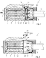
- FIG. 1 a section through a connector system 1 is shown.
- the connector system 1 has an electrical connector 2 and an electrical circuit 3, which is designed as a printed circuit board 3 in the exemplary embodiment.
- the connector 2 also has a longitudinal axis L, which runs along a plug-in direction, indicated in the figure by a double arrow.
- any electrical circuit can in principle be provided, for example in the form of a multi-chip module, a system-in-package, a system-on-chip and / or any integrated circuit, e.g. B. also a single microchip or ASIC.
- the invention is described in the exemplary embodiment using a printed circuit board 3, but this can be understood as a "black box" for any electrical circuit.
- the connector 2 has a housing 4, which in the present embodiment is made of a non-conductive material, for. B. is formed from a plastic.
- the housing 4 serves, among other things, to accommodate an electrical line 5, which in the exemplary embodiment is designed as a cable 5 that is held in the housing 4 of the plug connector 2 via a holding device 6.
- the cable 5 is an electrically shielded cable 5 with a ground conductor which is designed as an outer conductor 7, in particular as a braided shield 7, which is electrically conductively connected to a means for shielding 8 of the connector 2.
- the outer conductor 7 carries a defined electrical potential, in particular a ground potential, which is suitable for forming a shield.
- the braided shield 7 is clamped between the shielding means 8 and the housing 4 of the connector 2.
- the means for shielding 8 preferably extends completely around the inner regions of the connector 2 in order to shield the connector 2 completely electromagnetically.
- signal conductors 10 which in the exemplary embodiment are designed as inner cable conductors 10 of cable 5, are electrically connected at their ends facing circuit board 3 to contacts 9 on the input side.
- the connector 2 has contacts 11 on the output side, which are electrically connected to connector inner conductors 12.
- three contacts 9, 11 are provided in each case. The number can be arbitrary in the present case.
- the plug connector 2 has a receptacle 13 for the printed circuit board 3, which is designed as a slot-shaped recess 13 between the input-side contacts 9 and the output-side contacts 11.
- the receptacle 13 has an access opening 14 through which the circuit board 3 can be inserted.
- a closure element 15 is provided to close the access opening 14.
- the circuit board 3 has contact points 16, which in the present case are designed as flat contacts 16 or soldering areas which, in the case of the circuit board 3 used (as shown), make contact with the input-side contacts 9 and the output-side contacts 11.
- the circuit board 3 used is positioned between the input-side contacts 9 and the output-side contacts 11.
- the contacts 9, 11 of the plug connector 2 are designed as spring contacts 9, 11 in the present case.
- the circuit board 3 has conductor tracks, plated-through holes (not shown here) and electrical components 17 or electrical components. In this way, an individual transmission option from the input-side contacts 9 to the output-side contacts 11 can be guaranteed.
- the transmission options are diverse. Thus, for example, signal amplifications, impedance adjustments, linearizations up to an automatic adjustment with regard to the currently installed cable length and programmable circuits can be provided. It can also be provided that the printed circuit board 3 only has conductor tracks and / or plated-through holes, which enables a variable and quickly exchangeable assignment or rewiring of the plug connector 2.
- the housing 4 of the plug connector 2 optionally has a mechanical coding, by means of which the plug connector 2, which in the present case is designed as a plug, can be plugged into a socket (not shown), for example.
- the connector 2 can basically be a plug, a socket, a coupling or an adapter.
- the connector 2 can also be used as a printed circuit board connector or be accommodated in a device housing.
- the connector 2 can have contact sleeves 18 in its front area, which are electrically connected to the connector inner conductors 12.
- the closure element 15 is preferably formed essentially from plastic or from a non-conductive material and has an electrically conductive attachment 19 in the form of a contact spring attachment 19.
- the attachment 19 makes electrical contact with the shielding means 8 of the connector 2 and thus ensures a closed electromagnetic shielding.
- the closure element 15 comprises a seal 20 for mechanically sealing the access opening 14.
- a contact element 21 is also provided on the closure element 15, which, in the manner of an additional contact spring, electrically connects the electrically conductive attachment 19 of the closure element 15 to a circuit shield, in this case a circuit board shield 22 in the form of a metallized surface of the circuit board 3. Furthermore, a further contact element 23 of a similar design is provided at the lower end of the receptacle 13, which contact element also makes contact with the circuit board shielding 22 of the circuit board 3. In principle, electrical contacting of the shields 8, 19, 22 on all sides and over a large area is advantageous.
- one or all of the contact elements 21, 23 can also be provided on the circuit board 3 or on the circuit board shield 22.
- a printed circuit board shield 22 can also be implemented without necessarily providing electrical contact with the attachment 19 via the contact element.
- the circuit board 3 and in particular its sectional structure is shown only as an example and in a highly abstracted manner.
- the circuit board 3 can be a one-sided circuit board, a two-sided circuit board or a multilayer circuit board 3 with more than two circuit board layers.
- a circuit board 3 with two circuit board layers 26 is described later in FIG Figure 11 shown enlarged.
- the illustrated connector system 1 can advantageously be set up for the transmission of electrical signals according to a USB standard.
- FIG 2 is that in Figure 1 illustrated connector system 1 is shown again, wherein the circuit board 3 has been removed. Furthermore, the closure element 15 is not inserted into the access opening 14.
- the input-side contacts 9 and the output-side contacts 11 do not make electrical contact when the printed circuit board 3 is removed. This is a constructively preferable solution, since the implementation of such an arrangement is easy to handle. It can also be advantageous, by removing the printed circuit board 3, to effect a reliable galvanic separation of circuits within the plug connector 2. It can also be understood as in the context of the invention to provide a printed circuit board 3, which only ensures reliable galvanic separation between some or all of the contacts 9, 11.
- the printed circuit board 3 would accordingly have a transfer option or a transfer function of zero between at least one input-side contact 9 and at least one output-side contact 11.
- the circuit board 3 can thus also serve as a securing element - either in the inserted or removed state, depending on the design.
- the relaxed length of the springs when the contacts 9, 11 are designed as springs or the distances between the contacts 9, 11 are selected such that the input-side contacts 9 and the output-side contacts 11 themselves contact one another if the printed circuit board 3 is not inserted.
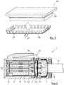
- FIG 3 is the closure element 15 of the Figures 1 and 2 enlarged and shown in a spatial representation.
- the closure element 15 is essentially formed from a non-conductive material and comprises the seal 20 already described.
- the conductive attachment 19 is preferably formed from a sheet metal and pushed or placed onto the closure element 15. Lateral contact springs 24 are provided, thereby ensuring reliable electrical contact with the outer conductor 7 of the cable 5 or with the means for shielding 8 of the connector 2 can be guaranteed even when large tolerances are to be compensated.
- the contact springs 24 are preferably arranged in a ring around the closure element 15. In a simplified design, however, a single contact or a single contact spring 24 can also be sufficient.
- closure element 15 is formed in a simplified embodiment as a sheet metal element or completely from metal.
- the closure element 15 is positively and non-positively connected to the means for shielding 8 of the plug connector 2 by, for example, a screw connection.
- the closure element 15 is preferably arranged set back in the inserted state in the housing 4 of the plug connector 2.
- a coplanar design or a design in which the closure element 15 protrudes from the housing 4 is also possible (see e.g. Figure 1 ), possible.
- FIG Figure 5 A third embodiment of a connector system 1 according to the invention is shown in FIG Figure 5 shown.
- the connector 2 is designed as a coupling.
- the contact sleeve or the contact sleeves 18 of the front area of the plug connector 2 is or are arranged in the embodiment in relation to the circuit board 3 in such a way that a corresponding plug is able to make direct contact with the output-side contact points 16 of the circuit board 3.
- the output-side contact 11 is formed by the corresponding plug, which can be viewed as a component of the present connector system 1.
- the corresponding plug makes contact with the at least one output-side contact 11 of the plug connector 2.
- the output-side contacts 11 and the plug connector inner conductors 12 would be formed in one piece with the contact sleeves 18.
- FIG. 6 to 8 Simplified circuit diagrams are shown to show three exemplary variants of the connector system 1 or to show examples of the various transmission options from the at least one input-side contact 9 to the at least one output-side contact 11.
- the input-side contact 9 of the connector 2 with the cable inner conductors 10 and the output-side contact 11 of the connector 2 with the connector inner conductors 12 and the printed circuit board 3 are shown in each case.
- the electrical contacting of the contacts 9, 11 of the connector 2 and the contact points 16 of the printed circuit board 3 are only shown very schematically.
- circuit board 3 functions only for the forwarding or direct contacting of the cable inner conductors 10 with the plug connector inner conductors 12.
- the circuit board 3 can only have vias for this purpose.
- the circuit board 3 and the transmission option then function as a so-called "dummy" element.
- Figure 7 is one of the Figure 6 A similar embodiment is shown, in which the printed circuit board 3 once again only serves to make contact between the cable inner conductors 10 and the connector inner conductors 12, without providing any further influencing of the signals. However, in this embodiment it is a "crossover" connection, ie a cross-connection of signals and thus one of the Figure 6 different connector assignment.
- the plug connection 2 can thus be functionally changed.
- Figure 8 shows a further embodiment in which an electronics 25 of the circuit board 3 - shown as a "black box” - electrically influences one or more or all of the signals when they are passed on from the input-side contacts 9 to the output-side contacts 11.
- the invention can also be used to avoid or replace a conventional fan-out area within a plug connector or to adapt an input-side interface 30 and an output-side interface 31 in an impedance-controlled manner.
- the so-called pitch i. H. a center-to-center distance of the contacts 9, 11 or contact points 16 can be modified.
- the cable inner conductors 10 are fanned out, d. H. the pitch is expanded in order to achieve the correct proportions for the connector.
- Such a fanning out can be clearly seen in FIGS. 1, 2, 4 and 5.
- the cable inner conductors 10 are usually fanned out so that their ends assume a position such that each end of a cable inner conductor 10 is assigned a corresponding end of a connector inner conductor 12 and the ends assigned to one another run coaxially to one another.
- any number of unbundling options for the input-side and output-side interfaces (“interfaces”) 30, 31 are possible.
- Any pin assignments or plug connector standards can be adapted with the electrical circuit or printed circuit board 3, with impedance control being possible at the same time by appropriate circuit components of the electrical circuit or printed circuit board 3. For example, it is possible to switch from a transmission type or "stranding" with a star quad to a parallel transmission type ("parallel pair").
- Figure 9 shows a further example of different interfaces 30, 31 on the input side and on the output side, each with a different pitch.
- the output-side interface 31 therefore has greater distances between the individual cores or connector inner conductors 12.
- a fan-out area which, however, causes faults in the transmission path.
- both interfaces 30, 31 can have the same impedance (e.g. 90 ohms differential).
- a circuit board 3 can be provided, it being possible to first make direct contact with the circuit board 3 from both sides with the respective interface dimensions.
- a suitable design of the microstrip lines and vias of the circuit board 3 can then compensate for the capacitive behavior of the transition from the respective inner conductors 10, 12 to the circuit board 3.
- a reflection-free pitch change is preferably provided.
- the receptacle 13 for the circuit board 3 is not shown for the sake of simplicity.
- the printed circuit board 3 can, however, be inserted into the plug connector 2 as described above.
- connector 2 is the Figure 9 shown as a printed circuit board connector. As shown, the connector 2 is not connected on the input side to a cable 5, but to a further printed circuit board 32. A plurality of electrical lines 5 or signal conductors 10 of the further printed circuit board 32 can be contacted with corresponding contact lines 33. Contact can also be made with a ground conductor of the further printed circuit board 32, if necessary, by means of at least one contact line 33.
- the contact lines 33 connect the signal conductors 10 to the contact points 16 of the printed circuit board 3 or to the contacts 9 on the input side.
- an electrical circuit By using an electrical circuit according to the invention, a transition between an input-side interface 30 and an output-side interface 31 that is optimally suitable for high-frequency technology can be provided, with differences between the interfaces 30, 31 that would have a negative effect on the signal transmission, such as, in particular, different line lengths , Center-to-center distances or relative positioning of the contacts, geometry or size the individual contacts and the type of material of the individual contacts, through which the correspondingly designed electrical circuit can be electrically balanced or adapted.
- Figure 11 shows a schematic sectional view of a circuit board 3 in an optional configuration as a circuit board 3, as this could be used for the present invention. It can also be a multilayer printed circuit board.
- the circuit board 3 according to Figure 11 comprises a full circumferential metallization 22 made of copper, which forms the circuit board shield 22, on its surfaces or side faces.
- the metallization 22 is cut out around the contact points 16 so as not to short-circuit the contact points 16 to the shield.
- circuit board layers 26 which are connected by means of contacts 27 and are spaced apart from one another, are arranged within the metallization 22.
- the circuit board layers 26 of the circuit board 3 are connected to the contact points 16 via plated-through holes 28.
- Electrical components 17 are preferably arranged in each case on the inwardly directed sides of the circuit board layers 26.
- the plated-through holes 28 and contacts 27 can also be formed in one piece.
- a thermally conductive layer 29 can be formed between the circuit board layers 26 and the electrical components 17 surrounding or immediately adjacent or adjoining.
- the distance between the circuit board layers 26 can depend, among other things, on the level and / or operating voltage of the electrical components 17 and on the electrical insulation capacity of the thermally conductive layer 29.
- the thermally conductive layer 29 can comprise epoxy resin. Due to the low thermal conductivity of epoxy resin, the thermally conductive layer 29 can also be enriched with boron nitride and / or aluminum oxide. Accordingly, the required thickness of the thermally conductive layer 29 can largely depend on its composition.
- epoxy resin instead of epoxy resin, synthetic resin can also be used accordingly. This is also particularly suitable.
- a connector 2 of the above-described embodiments of Figures 1, 2 and 4 to 10 also be designed in two parts.
Landscapes
- Engineering & Computer Science (AREA)
- Microelectronics & Electronic Packaging (AREA)
- Details Of Connecting Devices For Male And Female Coupling (AREA)
Claims (12)
- Système de connecteur (1) avec un connecteur électrique (2) pour la connexion d'au moins une ligne électrique (5), ainsi qu'avec un circuit électrique (3), dans lequel le connecteur électrique (2) comporte- au moins un contact d'entrée (9), pouvant être relié électriquement à une ligne de signal (10) de la ligne électrique (5),- au moins un contact de sortie (11), pouvant être relié électriquement à une ligne interne (12) du connecteur,- des moyens de blindage (8) pouvant être reliés électriquement à une ligne de masse (7) de ladite au moins une ligne électrique (5),- un logement (13) pour le circuit électrique (3), et- un élément de fermeture (15) pour la fermeture d'une ouverture d'accès (14) au logement (13), dans lequel le circuit électrique (3) comporte en outre des points de contact (16), pour relier au moins un contact d'entrée (9) avec au moins un contact de sortie (11), lorsque le circuit électrique (3) est disposé dans le logement (13), dans lequel le circuit électrique (3) est pourvu d'une possibilité de transmission dudit au moins un contact d'entrée (9) vers ledit au moins un contact de sortie (11),caractérisé, en ce que
l'élément de fermeture (15) est formé au moins en partie en un matériau conducteur de l'électricité et en ce que, lorsque l'élément de fermeture (15) ferme l'ouverture d'accès (14) au logement (13), il est en contact électrique avec les moyens de blindage (8) du connecteur (2). - Système de connecteur (1) selon la revendication 1,
caractérisé, en ce que
le circuit électrique (3) est réalisé sous la forme d'un circuit imprimé, de préférence un circuit imprimé double face, ou sous la forme d'un circuit imprimé multicouche avec plus de deux couches de circuit imprimé (26), d'un module à puces multiples, d'un système en boîtier, d'un système sur puce et/ou d'un circuit intégré. - Système de connecteur (1) selon l'une des revendications 1 ou 2,
caractérisé, en ce que
le circuit électrique (3), lorsqu'il est disposé dans le logement (13), est positionné entre ledit au moins un contact d'entrée (9) et ledit au moins un contact de sortie (11). - Système de connecteur (1) selon l'une des revendications 1, 2 ou 3,
caractérisé, en ce que
les points de contact (16) du circuit électrique (3) et/ou les contacts (9, 11) du connecteur (2) sont réalisés sous la forme de contacts plats et/ou de contacts à glissement et/ou de surfaces à braser et/ou de contacts à ressort et/ou de contacts enfichables. - Système de connecteur (1) selon l'une des revendications 1 à 4,
caractérisé, en ce que
si les contacts (9, 11) du connecteur (2) sont réalisés sous la forme de contacts à ressort, la longueur détendue des ressorts et/ou les distances entre les contacts (9, 11) est ou sont choisies de sorte que ledit au moins un contact d'entrée (9) et ledit au moins un contact de sortie (11) sont également en contact lorsque le circuit électrique (3) n'est pas présent dans le logement (13). - Système de connecteur (1) selon l'une des revendications 1 à 5,
caractérisé, en ce que
l'élément de fermeture (15) comporte au moins un ressort de contact (21) le mettant en contact électrique avec les moyens de blindage (8) du connecteur (2), lorsque l'élément de fermeture (15) ferme l'ouverture d'accès (14) au logement (13). - Système de connecteur (1) selon l'une des revendications 1 à 6,
caractérisé, en ce que
l'élément de fermeture (15) est réalisé en matière plastique avec une pièce rapportée (19) conductrice de l'électricité ou en métal. - Système de connecteur (1) selon l'une des revendications 1 à 7,
caractérisé, en ce que
l'élément de fermeture (15) comporte un joint (20) pour assurer l'étanchéité de l'ouverture d'accès (14). - Système de connecteur (1) selon l'une des revendications 1 à 8,
caractérisé, en ce que
l'élément de fermeture (15) peut être fixé par friction et/ou par liaison de matière et/ou par engagement positif dans un corps (4) du connecteur (2) et/ou dans le moyen de blindage (8) du connecteur (2) et/ou dans le logement (13), de préférence par coincement et/ou vissage et/ou collage et/ou brasage. - Système de connecteur (1) selon l'une des revendications 1 à 9,
caractérisé, en ce que
le circuit électrique (3) comporte un blindage de circuit (22), et en ce qu'au moins un élément de contact (21, 23) est ou sont prévus sur le moyen de blindage (8) du connecteur (2) et/ou sur la ligne de masse (7) de ladite au moins une ligne électrique (5) et/ou sur l'élément de fermeture (15) et/ou sur le circuit électrique (3), pour relier électriquement le blindage de circuit (22) et la ligne de masse (7) de ladite au moins une ligne électrique (5), lorsque le circuit électrique (3) est disposé dans le logement (13). - Système de connecteur (1) selon l'une des revendications 1 à 10,
caractérisé, en ce que
au moins un composant électrique (17) est intégré dans le circuit électrique (3), notamment dans le circuit imprimé, une couche conductrice de la chaleur (29) étant formée à proximité immédiate d'au moins un des composants électriques (17), et la couche conductrice de la chaleur (29) comportant un matériau support polymère isolant électriquement, notamment une résine synthétique et/ou une résine époxy et comportant en outre de l'oxyde d'aluminium et/ou du nitrure de bore. - Système de connecteur (1) selon l'une des revendications 1 à 11,
caractérisé, en ce que
le circuit électrique (3) comporte une interface d'entrée (30) avec au moins un point de contact d'entrée (16), afin de connecter ladite au moins une ligne de signal (10) de ladite au moins une ligne électrique (5), et le circuit électrique (3) comprenant une interface de sortie (31) avec au moins un point de contact de sortie (16), la possibilité de transmission étant prévue en particulier au moins pour le contrôle de l'impédance entre l'interface d'entrée (30) et l'interface de sortie (31), la conception de l'interface d'entrée (30) étant différente de la conception de l'interface de sortie (31).
Applications Claiming Priority (2)
| Application Number | Priority Date | Filing Date | Title |
|---|---|---|---|
| DE102017107248.9A DE102017107248A1 (de) | 2017-04-04 | 2017-04-04 | Steckverbindersystem |
| PCT/EP2018/058491 WO2018185102A1 (fr) | 2017-04-04 | 2018-04-03 | Système de connecteur enfichable |
Publications (2)
| Publication Number | Publication Date |
|---|---|
| EP3607619A1 EP3607619A1 (fr) | 2020-02-12 |
| EP3607619B1 true EP3607619B1 (fr) | 2021-08-04 |
Family
ID=61911584
Family Applications (1)
| Application Number | Title | Priority Date | Filing Date |
|---|---|---|---|
| EP18716207.8A Active EP3607619B1 (fr) | 2017-04-04 | 2018-04-03 | Système de connecteur enfichable |
Country Status (5)
| Country | Link |
|---|---|
| US (1) | US10840650B2 (fr) |
| EP (1) | EP3607619B1 (fr) |
| CN (1) | CN110476306B (fr) |
| DE (1) | DE102017107248A1 (fr) |
| WO (1) | WO2018185102A1 (fr) |
Cited By (2)
| Publication number | Priority date | Publication date | Assignee | Title |
|---|---|---|---|---|
| EP4546577A1 (fr) * | 2023-10-28 | 2025-04-30 | Harting International Innovation AG | Connexion capacitive à fiche |
| GB2639040A (en) * | 2024-03-08 | 2025-09-10 | Harting Int Innovation Ag | Capacitive plug connection |
Families Citing this family (4)
| Publication number | Priority date | Publication date | Assignee | Title |
|---|---|---|---|---|
| DE102017107251A1 (de) * | 2017-04-04 | 2018-10-04 | Rosenberger Hochfrequenztechnik Gmbh & Co. Kg | Elektrischer Steckverbinder mit einer elektrischen Schaltung |
| BE1026802B1 (de) * | 2018-11-26 | 2020-06-25 | Phoenix Contact Gmbh & Co | Steckverbinder |
| JP6866887B2 (ja) * | 2018-12-28 | 2021-04-28 | 株式会社オートネットワーク技術研究所 | 端子付き電線、端子モジュールおよびコネクタ |
| DE102020110237B4 (de) * | 2020-04-15 | 2021-11-18 | Md Elektronik Gmbh | Steckverbinderanordnung und verfahren zur herstellung einer steckverbinderanordnung |
Family Cites Families (26)
| Publication number | Priority date | Publication date | Assignee | Title |
|---|---|---|---|---|
| US4602429A (en) * | 1984-01-06 | 1986-07-29 | Burndy Corporation | Method and apparatus for assembling electrical connectors |
| JPH01134884A (ja) * | 1987-11-20 | 1989-05-26 | Nec Corp | Dteコネクタ |
| US5314346A (en) * | 1992-12-18 | 1994-05-24 | International Business Machines Corporation | Flexible circuit applique patch customization for generic programmable cable assemblies |
| US5442170B1 (en) * | 1994-04-15 | 1996-11-05 | Snap On Tech Inc | Programmable cable adaptor for connecting different automobile computers to diagnostic equipment |
| US5683261A (en) * | 1994-05-19 | 1997-11-04 | Spx Corporation | Removable coupling module for mechanically multiplexing conductors |
| JPH08293363A (ja) * | 1995-04-20 | 1996-11-05 | Nec Eng Ltd | 接続変換コネクタ |
| US5955703A (en) | 1996-02-28 | 1999-09-21 | Methode Electronics, Inc. | Circuitized electrical cable and method of assembling same |
| TW347153U (en) | 1997-10-16 | 1998-12-01 | Speed Tech Corp | Improved structure for socket of electron connector |
| JP2001143833A (ja) * | 1999-11-11 | 2001-05-25 | Yazaki Corp | 接続変換コネクタ |
| US6685505B1 (en) * | 2002-09-06 | 2004-02-03 | Hon Hai Precision Ind. Co., Ltd. | Electrical connector assembly having ground member |
| JP4266372B2 (ja) * | 2005-06-01 | 2009-05-20 | 日本航空電子工業株式会社 | コネクタ |
| CN201204330Y (zh) * | 2008-04-02 | 2009-03-04 | 富士康(昆山)电脑接插件有限公司 | 电连接器 |
| CN201197023Y (zh) * | 2008-04-08 | 2009-02-18 | 富士康(昆山)电脑接插件有限公司 | 电子卡连接器 |
| US7775833B1 (en) | 2008-06-27 | 2010-08-17 | Williams Pyro, Inc. | High speed intelligent cable |
| US7841902B2 (en) * | 2008-09-09 | 2010-11-30 | Hon Hai Precision Ind. Co., Ltd. | Electrical connector system with magnetic module |
| TWM363716U (en) * | 2008-12-22 | 2009-08-21 | nai-qian Zhang | A connection device with built-in digital TV turner |
| US7850492B1 (en) * | 2009-11-03 | 2010-12-14 | Panduit Corp. | Communication connector with improved crosstalk compensation |
| US8641452B2 (en) * | 2011-03-22 | 2014-02-04 | Panduit Corp. | Communication jack having an insulating element connecting a spring element and a spring end of a contact element |
| US9136647B2 (en) * | 2012-06-01 | 2015-09-15 | Panduit Corp. | Communication connector with crosstalk compensation |
| CN204696372U (zh) * | 2014-05-26 | 2015-10-07 | 富士康(昆山)电脑接插件有限公司 | 插座连接器 |
| JP5829311B1 (ja) * | 2014-06-18 | 2015-12-09 | ファナック株式会社 | ガス容器の密閉性を推定可能なガスレーザ発振器 |
| CN105789963B (zh) * | 2014-12-22 | 2018-06-01 | 富士康(昆山)电脑接插件有限公司 | Rj45插座连接器 |
| US9774111B2 (en) * | 2015-06-09 | 2017-09-26 | Molex, Llc | Cable connector assembly with multi-layered circuit board |
| CN106299890B (zh) * | 2015-06-09 | 2018-11-16 | 东莞莫仕连接器有限公司 | 线缆连接器 |
| CN105811138A (zh) * | 2016-05-11 | 2016-07-27 | 亳州联滔电子有限公司 | Usb插头 |
| CN205670612U (zh) * | 2016-06-15 | 2016-11-02 | 合肥京东方光电科技有限公司 | 一种电路转接装置 |
-
2017
- 2017-04-04 DE DE102017107248.9A patent/DE102017107248A1/de active Granted
-
2018
- 2018-04-03 EP EP18716207.8A patent/EP3607619B1/fr active Active
- 2018-04-03 US US16/497,898 patent/US10840650B2/en active Active
- 2018-04-03 CN CN201880022761.3A patent/CN110476306B/zh active Active
- 2018-04-03 WO PCT/EP2018/058491 patent/WO2018185102A1/fr not_active Ceased
Cited By (2)
| Publication number | Priority date | Publication date | Assignee | Title |
|---|---|---|---|---|
| EP4546577A1 (fr) * | 2023-10-28 | 2025-04-30 | Harting International Innovation AG | Connexion capacitive à fiche |
| GB2639040A (en) * | 2024-03-08 | 2025-09-10 | Harting Int Innovation Ag | Capacitive plug connection |
Also Published As
| Publication number | Publication date |
|---|---|
| CN110476306B (zh) | 2021-03-16 |
| EP3607619A1 (fr) | 2020-02-12 |
| WO2018185102A1 (fr) | 2018-10-11 |
| CN110476306A (zh) | 2019-11-19 |
| US10840650B2 (en) | 2020-11-17 |
| US20200106219A1 (en) | 2020-04-02 |
| DE102017107248A1 (de) | 2018-10-04 |
Similar Documents
| Publication | Publication Date | Title |
|---|---|---|
| EP3607619B1 (fr) | Système de connecteur enfichable | |
| EP3607618B1 (fr) | Connecteur enfichable électrique comprenant un circuit électrique | |
| DE69112669T2 (de) | Koppler zwischen einer Koaxialübertragungsleitung und einer Streifenleitung. | |
| DE3752310T2 (de) | Elektrische Steckverbinder | |
| EP3170229B1 (fr) | Connecteur et composant et utilisation du connecteur | |
| EP2695249B1 (fr) | Système de mise à la masse à action avancée au moyen d'un élément ressort | |
| EP3207640B1 (fr) | Connecteur enfichable pour la transmission capacitive de données | |
| EP3355419B1 (fr) | Connecteur enfichable destiné à relier un conducteur d'onde à au moins un conducteur électrique | |
| DE102012022747A1 (de) | Kontaktaugenfeder als Potenzialausgleichsleiterstück | |
| EP2510586A1 (fr) | Connecteur en relief et carte de circuits imprimés multicouche | |
| EP3163688B1 (fr) | Élément de connexion destiné à connecter un premier câble de données à un second câble de données et ligne de données comportant un tel élément de connexion. | |
| DE102020115922A1 (de) | Steckverbinder und Steckverbinderadapter zur mehrfachen symmetrischen Signalübertragung | |
| EP2595461B1 (fr) | Agencement doté d'une plaquette et d'un élément de connexion | |
| EP1997194B1 (fr) | Connecteur pour la transmission de données et les télécommunications | |
| EP3485540B1 (fr) | Câble muni d'un adaptateur | |
| DE102020119282B4 (de) | Kontaktvorrichtung | |
| EP3216089B1 (fr) | Interface électrique | |
| DE102014226888B4 (de) | Koppelvorrichtung zur kontaktfreien Übertragung von Datensignalen sowie Verfahren zur Übertragung von Datensignalen | |
| DE102013200635B4 (de) | Vorrichtung zur Aufnahme von Elektronikbauteilen | |
| WO2020048890A1 (fr) | Dispositif de distribution électrique, procédé de montage et système de transmission de signaux | |
| DE102015214258B4 (de) | Verbindermodul | |
| EP3382822B1 (fr) | Dispositif d'accouplement enfichable, procédé et utilisation | |
| EP3448135B1 (fr) | Fiche, douille enfichable et système de raccord correspondant | |
| DE19651800B4 (de) | Leitungs-Steckverbindung | |
| WO2022106553A1 (fr) | Connexion électrique enfichable, connecteur électrique et système de transmission de données |
Legal Events
| Date | Code | Title | Description |
|---|---|---|---|
| STAA | Information on the status of an ep patent application or granted ep patent |
Free format text: STATUS: UNKNOWN |
|
| STAA | Information on the status of an ep patent application or granted ep patent |
Free format text: STATUS: THE INTERNATIONAL PUBLICATION HAS BEEN MADE |
|
| PUAI | Public reference made under article 153(3) epc to a published international application that has entered the european phase |
Free format text: ORIGINAL CODE: 0009012 |
|
| STAA | Information on the status of an ep patent application or granted ep patent |
Free format text: STATUS: REQUEST FOR EXAMINATION WAS MADE |
|
| 17P | Request for examination filed |
Effective date: 20191022 |
|
| AK | Designated contracting states |
Kind code of ref document: A1 Designated state(s): AL AT BE BG CH CY CZ DE DK EE ES FI FR GB GR HR HU IE IS IT LI LT LU LV MC MK MT NL NO PL PT RO RS SE SI SK SM TR |
|
| AX | Request for extension of the european patent |
Extension state: BA ME |
|
| DAV | Request for validation of the european patent (deleted) | ||
| DAX | Request for extension of the european patent (deleted) | ||
| GRAP | Despatch of communication of intention to grant a patent |
Free format text: ORIGINAL CODE: EPIDOSNIGR1 |
|
| STAA | Information on the status of an ep patent application or granted ep patent |
Free format text: STATUS: GRANT OF PATENT IS INTENDED |
|
| INTG | Intention to grant announced |
Effective date: 20210412 |
|
| GRAS | Grant fee paid |
Free format text: ORIGINAL CODE: EPIDOSNIGR3 |
|
| GRAA | (expected) grant |
Free format text: ORIGINAL CODE: 0009210 |
|
| STAA | Information on the status of an ep patent application or granted ep patent |
Free format text: STATUS: THE PATENT HAS BEEN GRANTED |
|
| AK | Designated contracting states |
Kind code of ref document: B1 Designated state(s): AL AT BE BG CH CY CZ DE DK EE ES FI FR GB GR HR HU IE IS IT LI LT LU LV MC MK MT NL NO PL PT RO RS SE SI SK SM TR |
|
| REG | Reference to a national code |
Ref country code: GB Ref legal event code: FG4D Free format text: NOT ENGLISH |
|
| REG | Reference to a national code |
Ref country code: AT Ref legal event code: REF Ref document number: 1417970 Country of ref document: AT Kind code of ref document: T Effective date: 20210815 |
|
| REG | Reference to a national code |
Ref country code: CH Ref legal event code: EP |
|
| REG | Reference to a national code |
Ref country code: DE Ref legal event code: R096 Ref document number: 502018006422 Country of ref document: DE |
|
| REG | Reference to a national code |
Ref country code: IE Ref legal event code: FG4D Free format text: LANGUAGE OF EP DOCUMENT: GERMAN |
|
| REG | Reference to a national code |
Ref country code: SE Ref legal event code: TRGR |
|
| REG | Reference to a national code |
Ref country code: LT Ref legal event code: MG9D |
|
| REG | Reference to a national code |
Ref country code: NL Ref legal event code: MP Effective date: 20210804 |
|
| PG25 | Lapsed in a contracting state [announced via postgrant information from national office to epo] |
Ref country code: RS Free format text: LAPSE BECAUSE OF FAILURE TO SUBMIT A TRANSLATION OF THE DESCRIPTION OR TO PAY THE FEE WITHIN THE PRESCRIBED TIME-LIMIT Effective date: 20210804 Ref country code: ES Free format text: LAPSE BECAUSE OF FAILURE TO SUBMIT A TRANSLATION OF THE DESCRIPTION OR TO PAY THE FEE WITHIN THE PRESCRIBED TIME-LIMIT Effective date: 20210804 Ref country code: FI Free format text: LAPSE BECAUSE OF FAILURE TO SUBMIT A TRANSLATION OF THE DESCRIPTION OR TO PAY THE FEE WITHIN THE PRESCRIBED TIME-LIMIT Effective date: 20210804 Ref country code: HR Free format text: LAPSE BECAUSE OF FAILURE TO SUBMIT A TRANSLATION OF THE DESCRIPTION OR TO PAY THE FEE WITHIN THE PRESCRIBED TIME-LIMIT Effective date: 20210804 Ref country code: PT Free format text: LAPSE BECAUSE OF FAILURE TO SUBMIT A TRANSLATION OF THE DESCRIPTION OR TO PAY THE FEE WITHIN THE PRESCRIBED TIME-LIMIT Effective date: 20211206 Ref country code: NO Free format text: LAPSE BECAUSE OF FAILURE TO SUBMIT A TRANSLATION OF THE DESCRIPTION OR TO PAY THE FEE WITHIN THE PRESCRIBED TIME-LIMIT Effective date: 20211104 Ref country code: BG Free format text: LAPSE BECAUSE OF FAILURE TO SUBMIT A TRANSLATION OF THE DESCRIPTION OR TO PAY THE FEE WITHIN THE PRESCRIBED TIME-LIMIT Effective date: 20211104 Ref country code: LT Free format text: LAPSE BECAUSE OF FAILURE TO SUBMIT A TRANSLATION OF THE DESCRIPTION OR TO PAY THE FEE WITHIN THE PRESCRIBED TIME-LIMIT Effective date: 20210804 |
|
| PG25 | Lapsed in a contracting state [announced via postgrant information from national office to epo] |
Ref country code: PL Free format text: LAPSE BECAUSE OF FAILURE TO SUBMIT A TRANSLATION OF THE DESCRIPTION OR TO PAY THE FEE WITHIN THE PRESCRIBED TIME-LIMIT Effective date: 20210804 Ref country code: LV Free format text: LAPSE BECAUSE OF FAILURE TO SUBMIT A TRANSLATION OF THE DESCRIPTION OR TO PAY THE FEE WITHIN THE PRESCRIBED TIME-LIMIT Effective date: 20210804 Ref country code: GR Free format text: LAPSE BECAUSE OF FAILURE TO SUBMIT A TRANSLATION OF THE DESCRIPTION OR TO PAY THE FEE WITHIN THE PRESCRIBED TIME-LIMIT Effective date: 20211105 |
|
| PG25 | Lapsed in a contracting state [announced via postgrant information from national office to epo] |
Ref country code: NL Free format text: LAPSE BECAUSE OF FAILURE TO SUBMIT A TRANSLATION OF THE DESCRIPTION OR TO PAY THE FEE WITHIN THE PRESCRIBED TIME-LIMIT Effective date: 20210804 |
|
| PG25 | Lapsed in a contracting state [announced via postgrant information from national office to epo] |
Ref country code: DK Free format text: LAPSE BECAUSE OF FAILURE TO SUBMIT A TRANSLATION OF THE DESCRIPTION OR TO PAY THE FEE WITHIN THE PRESCRIBED TIME-LIMIT Effective date: 20210804 |
|
| REG | Reference to a national code |
Ref country code: DE Ref legal event code: R097 Ref document number: 502018006422 Country of ref document: DE |
|
| PG25 | Lapsed in a contracting state [announced via postgrant information from national office to epo] |
Ref country code: SM Free format text: LAPSE BECAUSE OF FAILURE TO SUBMIT A TRANSLATION OF THE DESCRIPTION OR TO PAY THE FEE WITHIN THE PRESCRIBED TIME-LIMIT Effective date: 20210804 Ref country code: SK Free format text: LAPSE BECAUSE OF FAILURE TO SUBMIT A TRANSLATION OF THE DESCRIPTION OR TO PAY THE FEE WITHIN THE PRESCRIBED TIME-LIMIT Effective date: 20210804 Ref country code: RO Free format text: LAPSE BECAUSE OF FAILURE TO SUBMIT A TRANSLATION OF THE DESCRIPTION OR TO PAY THE FEE WITHIN THE PRESCRIBED TIME-LIMIT Effective date: 20210804 Ref country code: EE Free format text: LAPSE BECAUSE OF FAILURE TO SUBMIT A TRANSLATION OF THE DESCRIPTION OR TO PAY THE FEE WITHIN THE PRESCRIBED TIME-LIMIT Effective date: 20210804 Ref country code: CZ Free format text: LAPSE BECAUSE OF FAILURE TO SUBMIT A TRANSLATION OF THE DESCRIPTION OR TO PAY THE FEE WITHIN THE PRESCRIBED TIME-LIMIT Effective date: 20210804 Ref country code: AL Free format text: LAPSE BECAUSE OF FAILURE TO SUBMIT A TRANSLATION OF THE DESCRIPTION OR TO PAY THE FEE WITHIN THE PRESCRIBED TIME-LIMIT Effective date: 20210804 |
|
| PLBE | No opposition filed within time limit |
Free format text: ORIGINAL CODE: 0009261 |
|
| STAA | Information on the status of an ep patent application or granted ep patent |
Free format text: STATUS: NO OPPOSITION FILED WITHIN TIME LIMIT |
|
| 26N | No opposition filed |
Effective date: 20220506 |
|
| PG25 | Lapsed in a contracting state [announced via postgrant information from national office to epo] |
Ref country code: SI Free format text: LAPSE BECAUSE OF FAILURE TO SUBMIT A TRANSLATION OF THE DESCRIPTION OR TO PAY THE FEE WITHIN THE PRESCRIBED TIME-LIMIT Effective date: 20210804 |
|
| REG | Reference to a national code |
Ref country code: CH Ref legal event code: PL |
|
| REG | Reference to a national code |
Ref country code: BE Ref legal event code: MM Effective date: 20220430 |
|
| PG25 | Lapsed in a contracting state [announced via postgrant information from national office to epo] |
Ref country code: MC Free format text: LAPSE BECAUSE OF FAILURE TO SUBMIT A TRANSLATION OF THE DESCRIPTION OR TO PAY THE FEE WITHIN THE PRESCRIBED TIME-LIMIT Effective date: 20210804 Ref country code: LU Free format text: LAPSE BECAUSE OF NON-PAYMENT OF DUE FEES Effective date: 20220403 Ref country code: LI Free format text: LAPSE BECAUSE OF NON-PAYMENT OF DUE FEES Effective date: 20220430 Ref country code: CH Free format text: LAPSE BECAUSE OF NON-PAYMENT OF DUE FEES Effective date: 20220430 |
|
| PG25 | Lapsed in a contracting state [announced via postgrant information from national office to epo] |
Ref country code: BE Free format text: LAPSE BECAUSE OF NON-PAYMENT OF DUE FEES Effective date: 20220430 |
|
| PG25 | Lapsed in a contracting state [announced via postgrant information from national office to epo] |
Ref country code: IE Free format text: LAPSE BECAUSE OF NON-PAYMENT OF DUE FEES Effective date: 20220403 |
|
| P01 | Opt-out of the competence of the unified patent court (upc) registered |
Effective date: 20230515 |
|
| PG25 | Lapsed in a contracting state [announced via postgrant information from national office to epo] |
Ref country code: MK Free format text: LAPSE BECAUSE OF FAILURE TO SUBMIT A TRANSLATION OF THE DESCRIPTION OR TO PAY THE FEE WITHIN THE PRESCRIBED TIME-LIMIT Effective date: 20210804 Ref country code: CY Free format text: LAPSE BECAUSE OF FAILURE TO SUBMIT A TRANSLATION OF THE DESCRIPTION OR TO PAY THE FEE WITHIN THE PRESCRIBED TIME-LIMIT Effective date: 20210804 |
|
| PG25 | Lapsed in a contracting state [announced via postgrant information from national office to epo] |
Ref country code: HU Free format text: LAPSE BECAUSE OF FAILURE TO SUBMIT A TRANSLATION OF THE DESCRIPTION OR TO PAY THE FEE WITHIN THE PRESCRIBED TIME-LIMIT; INVALID AB INITIO Effective date: 20180403 |
|
| REG | Reference to a national code |
Ref country code: AT Ref legal event code: MM01 Ref document number: 1417970 Country of ref document: AT Kind code of ref document: T Effective date: 20230403 |
|
| PG25 | Lapsed in a contracting state [announced via postgrant information from national office to epo] |
Ref country code: TR Free format text: LAPSE BECAUSE OF FAILURE TO SUBMIT A TRANSLATION OF THE DESCRIPTION OR TO PAY THE FEE WITHIN THE PRESCRIBED TIME-LIMIT Effective date: 20210804 |
|
| PG25 | Lapsed in a contracting state [announced via postgrant information from national office to epo] |
Ref country code: AT Free format text: LAPSE BECAUSE OF NON-PAYMENT OF DUE FEES Effective date: 20230403 |
|
| PG25 | Lapsed in a contracting state [announced via postgrant information from national office to epo] |
Ref country code: AT Free format text: LAPSE BECAUSE OF NON-PAYMENT OF DUE FEES Effective date: 20230403 |
|
| PG25 | Lapsed in a contracting state [announced via postgrant information from national office to epo] |
Ref country code: MT Free format text: LAPSE BECAUSE OF FAILURE TO SUBMIT A TRANSLATION OF THE DESCRIPTION OR TO PAY THE FEE WITHIN THE PRESCRIBED TIME-LIMIT Effective date: 20210804 |
|
| PGFP | Annual fee paid to national office [announced via postgrant information from national office to epo] |
Ref country code: DE Payment date: 20250428 Year of fee payment: 8 |
|
| PGFP | Annual fee paid to national office [announced via postgrant information from national office to epo] |
Ref country code: IT Payment date: 20250422 Year of fee payment: 8 |
|
| PGFP | Annual fee paid to national office [announced via postgrant information from national office to epo] |
Ref country code: FR Payment date: 20250424 Year of fee payment: 8 |
|
| PGFP | Annual fee paid to national office [announced via postgrant information from national office to epo] |
Ref country code: SE Payment date: 20250424 Year of fee payment: 8 |
|
| PGFP | Annual fee paid to national office [announced via postgrant information from national office to epo] |
Ref country code: GB Payment date: 20260325 Year of fee payment: 9 |
|
| PGFP | Annual fee paid to national office [announced via postgrant information from national office to epo] |
Ref country code: AT Payment date: 20260410 Year of fee payment: 5 |