EP3207640B1 - Connecteur enfichable pour la transmission capacitive de données - Google Patents
Connecteur enfichable pour la transmission capacitive de données Download PDFInfo
- Publication number
- EP3207640B1 EP3207640B1 EP15793714.5A EP15793714A EP3207640B1 EP 3207640 B1 EP3207640 B1 EP 3207640B1 EP 15793714 A EP15793714 A EP 15793714A EP 3207640 B1 EP3207640 B1 EP 3207640B1
- Authority
- EP
- European Patent Office
- Prior art keywords
- plug connector
- signal transmission
- connector
- transmission means
- insulating body
- Prior art date
- Legal status (The legal status is an assumption and is not a legal conclusion. Google has not performed a legal analysis and makes no representation as to the accuracy of the status listed.)
- Active
Links
Images







Classifications
-
- H—ELECTRICITY
- H04—ELECTRIC COMMUNICATION TECHNIQUE
- H04B—TRANSMISSION
- H04B5/00—Near-field transmission systems, e.g. inductive or capacitive transmission systems
- H04B5/20—Near-field transmission systems, e.g. inductive or capacitive transmission systems characterised by the transmission technique; characterised by the transmission medium
- H04B5/22—Capacitive coupling
-
- H—ELECTRICITY
- H01—ELECTRIC ELEMENTS
- H01R—ELECTRICALLY-CONDUCTIVE CONNECTIONS; STRUCTURAL ASSOCIATIONS OF A PLURALITY OF MUTUALLY-INSULATED ELECTRICAL CONNECTING ELEMENTS; COUPLING DEVICES; CURRENT COLLECTORS
- H01R24/00—Two-part coupling devices, or either of their cooperating parts, characterised by their overall structure
- H01R24/38—Two-part coupling devices, or either of their cooperating parts, characterised by their overall structure having concentrically or coaxially arranged contacts
- H01R24/40—Two-part coupling devices, or either of their cooperating parts, characterised by their overall structure having concentrically or coaxially arranged contacts specially adapted for high frequency
- H01R24/42—Two-part coupling devices, or either of their cooperating parts, characterised by their overall structure having concentrically or coaxially arranged contacts specially adapted for high frequency comprising impedance matching means or electrical components, e.g. filters or switches
-
- H—ELECTRICITY
- H01—ELECTRIC ELEMENTS
- H01R—ELECTRICALLY-CONDUCTIVE CONNECTIONS; STRUCTURAL ASSOCIATIONS OF A PLURALITY OF MUTUALLY-INSULATED ELECTRICAL CONNECTING ELEMENTS; COUPLING DEVICES; CURRENT COLLECTORS
- H01R13/00—Details of coupling devices of the kinds covered by groups H01R12/70 or H01R24/00 - H01R33/00
- H01R13/646—Details of coupling devices of the kinds covered by groups H01R12/70 or H01R24/00 - H01R33/00 specially adapted for high-frequency, e.g. structures providing an impedance match or phase match
- H01R13/6461—Means for preventing cross-talk
- H01R13/6464—Means for preventing cross-talk by adding capacitive elements
- H01R13/6466—Means for preventing cross-talk by adding capacitive elements on substrates, e.g. printed circuit boards [PCB]
-
- H—ELECTRICITY
- H04—ELECTRIC COMMUNICATION TECHNIQUE
- H04B—TRANSMISSION
- H04B5/00—Near-field transmission systems, e.g. inductive or capacitive transmission systems
- H04B5/70—Near-field transmission systems, e.g. inductive or capacitive transmission systems specially adapted for specific purposes
-
- H—ELECTRICITY
- H04—ELECTRIC COMMUNICATION TECHNIQUE
- H04B—TRANSMISSION
- H04B5/00—Near-field transmission systems, e.g. inductive or capacitive transmission systems
- H04B5/70—Near-field transmission systems, e.g. inductive or capacitive transmission systems specially adapted for specific purposes
- H04B5/72—Near-field transmission systems, e.g. inductive or capacitive transmission systems specially adapted for specific purposes for local intradevice communication
Definitions
- the invention is based on a connector according to the preamble of independent claim 1.
- the invention also relates to a system comprising a connector and a mating connector.
- Such connectors transmit signals and / or data without the respective signal transmission means being in direct contact with one another.
- Such systems consisting of connectors and mating connectors are used in particular when many mating cycles are to be achieved.
- the signal-transmitting elements are not subject to wear.
- the DE 10 2010 045 742 A1 shows a coupling with means, here coils, for the inductive transmission of data signals.
- the document EP 1 206 012 A1 describes a connector comprising a plug element and a socket element which can be detachably connected to the plug element, for connecting a transmission line to at least one sensor. So that when the plug element and socket element are connected to one another, moisture, dust or dirt particles and aggressive substances penetrating between the plug element and the socket element and aggressive substances do not impair the signal transmission between the plug element and the socket element EP 1 206 012A1 before that the connector has means for realizing a contactless signal transmission between the plug element and the socket element. In particular, inductive, capacitive or optical signal transmission is intended.
- a plug connection according to DE 197 19 730 C1 For a potentially explosive area for energy and data transmission by means of electrical quantities in a bus system, a primary part designed as a transmitter and a secondary part and limiting devices for electrical quantities to be transmitted have.
- the limiter devices are arranged in the primary part and are designed to limit the electrical quantities to be transmitted to the secondary part to values permissible for the respective type of protection.
- the object of the invention is to propose a connector that shows good performance in a wide frequency range and at the same time has a compact design.
- a multi-core cable with at least two or more individual conductors can be connected to the connector according to the invention.
- the connector has at least one signal transmission means, which for contactless signal transmission is provided.
- non-contact signal transmission means that the signal transmission means of a plug connector and a matching mating connector do not physically touch each other.
- Contactless could also mean that there is simply no electrically conductive connection between the signal transmission means.
- the plug connector has a microchip which is connected on the one hand to the signal transmission means or to the signal transmission means and on the other hand can be electrically connected to the individual conductors of the connected cable.
- the signal transmission means are ring capacitors and / or plate capacitors. This enables a space-saving design. In addition, the twist between connector and mating connector is not relevant due to such signal transmission means. The signals are always transmitted equally well.
- the microchip is an active microchip.
- the microchip requires a power supply that is fed, for example, by the incoming conductor. But there can also be a separate power supply, for example a battery, in the connector be provided.
- the microchip can process and forward incoming signals using a so-called multiplexing method. As a result, a large number of incoming conductors and associated signals can be forwarded by only one signal transmission element.
- an inductive signal transmission means is assigned to each incoming conductor. With a multi-core cable, a connector would be very complex.
- the microchip is also able to adapt the transmission power of the signal transmission means, depending on the distance between the connector and the mating connector. This means that it is not necessary to maintain an exact distance between the connector and mating connector.
- the active microchip makes it possible to cover a wide frequency range from binary signals up to high data transfer rates in the megabit range or the associated frequencies.
- the connector has two signal transmission means.
- One signal transmission means is provided for sending the signals arriving at the connector via the connected cable.
- the other signal transmission means is provided for receiving the signals coming in from the mating connector. Thanks to the active microchip, the connector proposed here requires only two signal transmission means, which enables a simple and compact construction of the connector.
- One signal transmission means is designed as a ring capacitor and the other signal transmission means as a circular capacitor plate. This geometry allows the signal transmission means to be plugged into the end face of the connector.
- the ring capacitor and the circular capacitor plate preferably have an equally large surface area.
- the transmission and reception function of the connector according to the invention is thereby optimized.
- the connector according to the invention is insensitive to interference since the signals and / or data are not transmitted by radio.
- the plug connector has a plug connector housing, the end faces of which form a plug side and a connection side.
- the signal transmission means are advantageously completely enclosed by the plug-in side of the housing.
- the signal transmission means or the capacitors described above are arranged on the front side of the connector facing the direction of insertion and are covered there with a plastic material. This is achieved, for example, by an injection molding process. This protects the signal transmission means from environmental influences. This enables the connector to be used in dirty and harsh environments. When unplugged, the individual connector is longitudinally watertight and fulfills protection class IP6x.
- the signal transmission means is preferably aligned on the plug side parallel to the end face of the connector. This enables connectors and mating connectors to optimally exchange signals and data.
- the plug connector has an insulating body which has at least one conductor channel which is electrically connected on one side to the microchip and on the other side can be electrically connected to a conductor of the connected cable.
- the at least one conductor channel is preferably produced using MID technology.
- the number of conductor channels is preferably matched to the number of incoming conductors of the multi-core cable and the signal transmission means. As a rule, several such conductor channels are therefore provided.
- the MID technology enables a compact design of the connector.
- a spring element preferably a spiral spring, is advantageously arranged in the connector housing in such a way that the spring force of the spring element presses the insulating body axially in the plug-in direction of the connector.
- the spring acts on an end face of the insulating body. The other end of the insulating body is thereby pressed to the plug-in side of the connector housing and fits snugly there. As already described above, this end face also has the signal transmission means.
- the respective signal transmission means are aligned parallel to one another when plugged in.
- the signal and data transmission works best.
- the invention also relates to a system of plug-in connectors and mating plug-in connectors, both of which each have at least one signal transmission means, the respective signal transmission means being aligned parallel to one another when plugged in.
- the signal transmission means are preferably at a distance of 1.1 millimeters (mm) or less from one another when plugged in. This distance enables good signal and data transmission.
- connectors and / or the mating connector of the system are ideally designed like the connector claimed according to the invention.
- Connectors and mating connectors can also be constructed identically.
- connectors and mating connectors are also referred to as connectors.
- the connector and the mating connector are preferably connected to one another via a so-called push-pull connection.
- a push-pull connection is particularly ideal for high-frequency applications because of the high level of vibration protection.
- the hermaphroditic design of the insulating body of the connector and mating connector makes it particularly easy to implement a push-pull connection. It is not necessary to pay attention to a special alignment of the mating faces to each other, within the axis of rotation.
- the connector design proposed here allows high mating tolerances.
- the possibly different distance between the signal transmission means can be compensated for by the active chip.
- a system which is operated with a plug connector according to the invention always has a so-called galvanic isolation, since the signal transmission means of the plug and mating plug or socket have no physical contact.
- the Figure 1 shows a connector 1, which is connected (plugged) with a matching mating connector 2 for signal transmission.
- the connector and mating connector shown here is intended for contactless signal transmission.
- the signal transmission takes place here essentially by capacitive means, whereby inductive components can naturally always play a role. The latter, however, play an insignificant role here, if at all.
- the invention explicitly avoids an antenna function of the signal transmission means, in order to ensure, among other things, that the signals / data are secure against eavesdropping.
- the mating connector 2 consists of an insulating body, a housing 4, a cable outlet 5 and a screw sleeve 6.
- the mating area of the mating connector 2 is sealed by a sealing ring 7.
- the insulating body 3 is permanently moved in the direction of the plug-in area with the aid of a spiral spring 8, which is supported on the cable outlet 5 pressed. This ensures that the end face of the insulating body 3 which is relevant for the signal transport is arranged near the plug-in area of the mating connector 2.
- the screw sleeve 6 is fixed to the housing 4 with the aid of fixing plates 9.
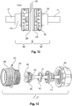
- the Figure 3 shows a perspective exploded view of the connector 1. Identical functional parts are provided with the same reference numerals here as with the mating connector 2.
- the insulating body 3 is pressed in the direction of insertion by a spiral spring 8.
- the housing 4 of the connector 1 has an external thread which interacts with an internal thread of the screw sleeve 6 of the mating connector 2 in such a way that the connectors (connector 1 and mating connector 2) are connected to one another and the end faces of the respective insulating bodies 3 are roughly parallel and in a defined manner Are aligned with each other.
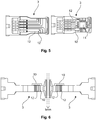
- the Figure 5 shows once the top and once the bottom of the insulating body 3, which is installed in both the connector 1 and the mating connector 2.
- the insulating body 3 has a multiplicity of individual conductor channels 12, which are implemented using MID technology. As a result, the guidance of the channels 12 can be made very flexible, which leads to a small component (insulating body 3).
- Some conductor channels open at a place 11 which is provided for the application of a microchip 10.
- the microchip 10 can process incoming or outgoing data signals as desired.
- the microchip 10 is able to forward the incoming signals using a multiplex method.
- FIGS. 7 to 9 show an alternative embodiment of a connector 1 ', 2' according to the invention.
- Two signal transmission means 13, 14 are introduced into the front of the insulating body 3 '.
- One signal transmission means 13 is ring-shaped and the other signal transmission means 14 is designed as a circular plate.
- Both signal transmission means 13, 14 have the same area dimensions and a connecting element 15 projecting perpendicularly to the basic shape.
- the connecting element 15 is bent to fix the antennas 13, 14 over a fixing surface 16 in the insulating body 3 '.
- the plug 1 ', 2' has a circuit card 17, which in turn has recesses 18.
- the insulating body 3 ' has latching arms 17, which latch in place in the recesses 18 with the insulating body 3' in order to fix the circuit board 17.
- a microchip 10 is applied to the circuit card and is in electrical contact with the signal transmission means 13, 14 and the connected conductors 20.
- the circuit board 17 has so-called solder pads 19, which are provided for the solder connection of the conductor 20 of a (multi-core) cable 21.
- the plug 1 ', 2' has a fixing element 25.
- the fixing element 25 is connected on one side to the printed circuit board 17.
- clamping tabs 24 and a tongue 23 arranged in between are provided on the fixing element, the tongue engaging in a recess 22 in the printed circuit board 17.
- the other side of the fixing element 25 consists of a ring part 26 with fixing arms 27 projecting radially therefrom, which are slightly bent at the ends and pressed against the cable sheath of the connected cable 21 to relieve the cable strain.
- the fixing element also serves to transfer the shield to the connected cable.
- the housing of the connector 1 ', 2' can be designed in different ways.
- the shape of the housing is not relevant to the invention, therefore only the screw part 28 is in Figure 9 shown.
- FIG 10 An elementary component of a third variant of the connector 1 according to the invention can be seen. This is a circular circuit board 29.
- printed circuit boards consist of electrically insulating material with adhering, conductive connections (conductor tracks). Fiber-reinforced plastic is common as an insulating material. The conductor tracks are mostly etched from a thin layer of copper. The components are soldered on so-called soldering pads.
- the first side 29a of the printed circuit board 29 comprises the signal transmission elements which are formed from a copper layer as described above.
- the second side 29b of the circuit board 29 has a mounting location 30 for the microchip 10 already mentioned several times above.
- solder pads 31, clamping points 31 or electrical contacting points 31 for insulation displacement terminals 32 are provided here.
- the insulation displacement contacts 32 are electrically contacted and mechanically fixed.
- FIG 11 the components can be seen that together produce the insulating body of the connector 1.
- a cable manager can be seen, which is essentially formed from a cylindrical plastic part.
- holding channels 34 are provided, into which the conductors 20 of the connected cables 21 can be clamped.
- annular contacting element 35 which has recesses into which insulation displacement clamps 32 are inserted.
- the cable manager 33 has fixing arms 36 with window-like openings which cooperate with fixing webs 37 of the contacting element 35 in such a way that these components 33, 34 are fixed to one another.
- the insulation displacement terminals 32 and associated conductor tracks of the printed circuit board 29 (not shown) establish electrical contact between the conductors 20 and the microchip 10.
- the connector 1 consists of a screw head 40 on the cable side.
- a combined sealing and strain relief element 41 is positioned in the screw head 40.
- a wave spring ring 42 is arranged, which essentially fulfills the same task as the spiral spring 8 described above of the first two exemplary embodiments of the connector 1, 1'.
- a double screw head 43 is provided on the plug side, one thread 44 of which can be connected to the screw head 40.
- the opposite thread 45 is provided for fixing with a mating connector.
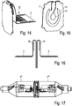
- Figure 14 shows a perspective view of an insulating body 3 of a first embodiment.
- the insulating body 3 is designed as a flexible printed circuit board, which is folded into itself and in this respect in a side view (see Figure 16 ) has a shape that substantially corresponds to a "T".
- solder pads 19 of the insulating body 3 can also be seen.
- Figure 15 shows a partial view of the insulating body 3 from Figure 14 from a different perspective with two signal transmission means 13, 14.
- the signal transmission means 13, 14 are essentially ring-shaped (signal transmission means 13) or circular (signal transmission means 14), the circular signal transmission means 14 being arranged concentrically with the substantially ring-shaped signal transmission means 13.
- the signal transmission means 13, 14 are arranged on the side of the insulating body 3, which in Figure 14 the opposite to the vertically arranged end part in the illustration opposite.
- Figure 16 shows a side view of two mutually arranged insulating bodies 3 of the first embodiment.
- the insulating bodies 3 each have a shape in the side view which essentially corresponds to a "T", the respective insulating body 3 being folded over itself in one half of the sweeping bar of the "T".
- the microchip 10 is arranged in each of these folding areas, and is therefore located opposite the signal transmission means 13, 14.
- Figure 17 is a view of connector 1 '"and mating connector 2'" of the first embodiment.
- Figure 18 is a perspective view of an insulating body 3 'of a second embodiment.
- the insulating body 3 ' is designed as a flexible printed circuit board
- the in Figure 18 Insulating body 3 'shown instead of in example Figure 14 recognizable folded area of the insulating body shown there has an essentially tubular area, on each of which ring-shaped signal transmission means 13 'and 14' are provided.
- Figure 18 shows a perspective view of another insulating body 3 "of the second exemplary embodiment.
- the basic structure of the insulating body 3" essentially corresponds to the insulating body 3 'of FIG Figure 18 is shown, but the signal transmission means 13 ", 14", which are also strip-shaped and bent into rings, are arranged on the inside of the tubular part of the insulating body 3 ", while the signal transmission means 13 ', 14' of the insulating body 3 'extend Figure 18 located on the outside of the tubular area.
- Figure 20 shows a side view of two mutually arranged insulating bodies 3 ', 3 "of the second exemplary embodiment Figure 20 can be seen, the insulating body 3 ', 3 ", which in Figure 18 and 19 are shown for coupling to one another in the form of a male coupling element (see Figure 18 ) and a female coupling element (see Figure 19 ) designed.
- the signal transmission means 13 ', 14' and 13 ", 14" are opposite each other, however, without direct contact being provided.
- the signal transmission means 13', 13", 14 ', 14 " can also each be on the outside or inside of the tubular part of the insulating body 3', 3 "be arranged. If the flexible printed circuit board is sufficiently thin, a reversal can also be made in that the female coupling component carries its signal transmission means on the outside and the male coupling component carries its signal transmission means on the inside.
- Figure 21 shows a view of connector 1 "" and mating connector 2 "" of the second embodiment. For further details, see the Figures 25 , 32 and 33 referred.
- Figures 22 to 24 each show partial views of an insulating body 3 of the first or second embodiment.
- the insulating body 3 which is designed in the form of a flexible printed circuit board, has conductor tracks 46 on both sides, with which overall space savings can be achieved. In order to enable adequate contacting, through holes 47 are provided so that a conductor track 46 is connected to a corresponding conductor track 46 on the opposite side of the insulating body 3.
- Figure 25 shows a perspective view of an insulating body 3 'of the second embodiment with a cable connector 48 attached to it.
- One way of contacting the solder pads 19 with the conductors of the cable is to attach a cable connector, for example an H-Flex SMT connector, to which a corresponding cable connector mating connector can then be coupled, with which the Head of the cable 21 are connected.
- a cable connector for example an H-Flex SMT connector
- Figure 26 shows a perspective view of an insulating body 3 of the first embodiment with attached cable connector 48, 49 with connected cable 21.
- the cable 21 is attached directly or indirectly to the insulating body 3, 3 ', 3 "of the first or second exemplary embodiment, the cable and the insulating body can be cast together in a suitable material, so that a desired sealing of the overall arrangement can be achieved offers protection against the influence of moisture or similar.
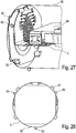
- Figure 27 and Figure 28 are views illustrating an embedding of the insulating body 3 of the first embodiment.
- the insulating body 3 with attached cable connector 48 which is enclosed in a sealing compound 50.
- the insulating body 3 has holding ears 51 which, in the form of embedding, make it possible to fix the end region of the insulating body 3 in the desired manner, in particular in such a way that there is sufficient parallelism with the end face.
- Recesses 2 which can also be recognized, result from the provision of corresponding wall projections in the form through which the end region of the insulating body 3 is pressed against the molding surface.
- the holding ears 51 of the insulating body 3 are also in Figure 28 to recognize.
- bayonet buttons 53 are provided when forming the potting compound.
- FIGS 29, 30 and 31 show perspective views of the connector 1 '"and the mating connector 2'" of the first embodiment.
- the in Figure 29 shown mating connector 2 '"bayonet knobs 53 during the in Figure 30 has shown connector 1 '"on a corresponding projecting part bayonet slots 54, in which the bayonet buttons 53 can engage in order to achieve a fixation of connector 1" and mating connector 2 "" to each other, as shown in Figure 31 is shown.
- Figure 32 and Figure 33 show perspective views of the connector 1 "" and the mating connector 2 "" of the second embodiment.
- the insulating body of the connector 1 '"and the insulating body of the mating connector 2" are each sealed in a suitable manner, the sealing in the case of the connector 1" “having a longitudinal slot, which allows flexibility with regard to deformation to widen the annular area
- the connector 1 "" has an annular projection in the end region which runs around on the inside.
- the mating connector 2 "" has an annular groove 57 at a corresponding point with which the ring projection 56 can be brought into engagement in order to achieve a certain fixation of the connector 1 "" and mating connector 2 "" with one another.
Landscapes
- Engineering & Computer Science (AREA)
- Computer Networks & Wireless Communication (AREA)
- Signal Processing (AREA)
- Details Of Connecting Devices For Male And Female Coupling (AREA)
- Near-Field Transmission Systems (AREA)
Claims (10)
- Connecteur enfichable (1, 1"', 1""), au niveau duquel un câble (21) multiconducteur avec au moins deux conducteurs (20) individuels ou plus peut être raccordé,- dans lequel le connecteur enfichable (1, 1"', 1"") présente sur un côté d'un corps isolant (3) du connecteur enfichable (1, 1"', 1"") deux moyens de transmission de signaux (13, 14, 13', 14', 13", 14") pour la transmission de signaux sans contact,- dans lequel le connecteur enfichable (1, 1"', 1"") présente une micro-puce (10), dans lequel la micro-puce (10) peut être reliée électriquement aux conducteurs (20) individuels et est reliée électriquement aux moyens de transmission de signaux (13, 14, 13', 14', 13", 14"),dans lequel la micro-puce (10) est une micro-puce (10) active, qui est configurée pour traiter et transmettre des signaux entrants selon un procédé de multiplexage,
dans lequel un moyen de transmission de signaux est réalisé en tant que condensateur annulaire (13, 13', 13") et l'autre moyen de transmission de signaux est réalisé en tant que plaque de condensateur circulaire (14, 14', 14"),
dans lequel la plaque de condensateur circulaire (14, 14', 14") est agencée concentriquement avec le condensateur annulaire (13, 13', 13"),
dans lequel le corps isolant (3) présente dans une vue latérale une forme, qui correspond sensiblement à un « T », dans lequel le corps isolant (3) est plié sur lui-même dans une moitié d'une barre transversale du « T », dans lequel la micro-puce (10) est agencée dans cette zone de pliage et ainsi fait face aux moyens de transmission de signaux (13, 14, 13', 14', 13", 14"). - Connecteur enfichable selon la revendication 1,
caractérisé en ce que
le condensateur annulaire (13, 13', 13'') et la plaque de condensateur circulaire (14, 14', 14'') présentent une surface de même taille. - Connecteur enfichable selon l'une quelconque des revendications précédentes,
caractérisé en ce- que le connecteur enfichable (1, 1''', 1'''') présente un boîtier de connecteur enfichable (4), dans lequel un côté enfichage et un côté raccordement sont réalisés au niveau de ses surfaces frontales,- et que les moyens de transmission de signaux (13, 14, 13', 14', 13", 14'') du côté enfichage du boîtier sont entièrement enfermés. - Connecteur enfichable selon l'une quelconque des revendications précédentes,
caractérisé en ce que
le moyen de transmission de signaux (13, 14, 13', 14', 13'', 14'') est orienté côté enfichage parallèlement à la surface frontale du connecteur enfichable (1, 1''', 1''''). - Connecteur enfichable selon l'une quelconque des revendications précédentes,
caractérisé en ce que
le corps isolant (3) présente au moins un canal de conducteurs (12), qui est relié d'un côté électriquement à la micro-puce (10) et peut être relié de l'autre côté électriquement à un conducteur (20) du câble (21) raccordé. - Connecteur enfichable selon la revendication 5,
caractérisé en ce que
l'au moins un canal de conducteurs (12) est fabriqué à l'aide de la technique MID. - Connecteur enfichable selon l'une quelconque des deux revendications précédentes,
caractérisé en ce que
un élément ressort, de préférence un ressort hélicoïdal (8), est agencé dans le boîtier de connecteur enfichable (4) de sorte que la force de ressort de l'élément ressort pousse le corps isolant (3) axialement dans la direction d'enfichage du connecteur enfichable (1, 2). - Système connecteur enfichable (1, 1''', 1'''') et contre-connecteur enfichable (2, 2''', 2''''), qui sont réalisés tous deux respectivement selon l'une quelconque des revendications 1 à 7,
caractérisé en ce que
les moyens de transmission de signaux (13, 14, 13', 14', 13'', 14'') respectifs sont orientés parallèlement l'un à l'autre à l'état enfiché. - Système connecteur enfichable (1, 1''', 1'''') et contre-connecteur enfichable (2, 2''', 2'''') selon la revendication 8,
caractérisé en ce que
les moyens de transmission de signaux (13, 14) à l'état enfiché ont une distance de 1,1 millimètre (mm) ou moins l'un par rapport à l'autre. - Système connecteur enfichable et contre-connecteur enfichable selon l'une quelconque des deux revendications précédentes,
caractérisé en ce que
le connecteur enfichable (1, 1''', 1'''') et le contre connecteur enfichable (2, 2''', 2'''') sont reliés l'un à l'autre par le biais d'un verrouillage push-pull.
Applications Claiming Priority (2)
| Application Number | Priority Date | Filing Date | Title |
|---|---|---|---|
| DE102014115122.4A DE102014115122A1 (de) | 2014-10-17 | 2014-10-17 | Steckverbinder zur kapazitiven Datenübertragung |
| PCT/EP2015/073427 WO2016058946A1 (fr) | 2014-10-17 | 2015-10-09 | Connecteur enfichable pour la transmission capacitive de données |
Publications (2)
| Publication Number | Publication Date |
|---|---|
| EP3207640A1 EP3207640A1 (fr) | 2017-08-23 |
| EP3207640B1 true EP3207640B1 (fr) | 2020-03-11 |
Family
ID=54540011
Family Applications (1)
| Application Number | Title | Priority Date | Filing Date |
|---|---|---|---|
| EP15793714.5A Active EP3207640B1 (fr) | 2014-10-17 | 2015-10-09 | Connecteur enfichable pour la transmission capacitive de données |
Country Status (7)
| Country | Link |
|---|---|
| US (1) | US20170244449A1 (fr) |
| EP (1) | EP3207640B1 (fr) |
| JP (1) | JP2017534200A (fr) |
| KR (1) | KR102454999B1 (fr) |
| CN (1) | CN107078445B (fr) |
| DE (1) | DE102014115122A1 (fr) |
| WO (1) | WO2016058946A1 (fr) |
Families Citing this family (21)
| Publication number | Priority date | Publication date | Assignee | Title |
|---|---|---|---|---|
| AU2015249322B2 (en) | 2014-04-25 | 2020-01-30 | Bayer Healthcare Llc | Syringe with rolling diaphragm |
| JP6731943B2 (ja) | 2015-04-24 | 2020-07-29 | バイエル・ヘルスケア・エルエルシーBayer HealthCare LLC | まくりダイアフラムを有するシリンジ |
| CA3036818C (fr) | 2016-09-16 | 2024-01-09 | Bayer Healthcare Llc | Enveloppe de pression ayant un element de retenue de seringue |
| US11547793B2 (en) | 2016-10-17 | 2023-01-10 | Bayer Healthcare Llc | Fluid injector with syringe engagement mechanism |
| AU2017345167B2 (en) | 2016-10-17 | 2022-12-15 | Bayer Healthcare Llc | Fluid injector with syringe engagement mechanism |
| WO2019055497A1 (fr) | 2017-09-13 | 2019-03-21 | Bayer Healthcare Llc | Capuchon coulissant de seringue pour remplissage et distribution séparés |
| CN107705983B (zh) * | 2017-09-30 | 2019-03-01 | 铜陵兴怡金属材料有限公司 | 一种电容器插拔式连接装置 |
| EP4385541A3 (fr) | 2018-02-19 | 2024-09-11 | Bayer HealthCare LLC | Appareil et procédé de roulement de seringue |
| AU2019340438A1 (en) | 2018-09-11 | 2021-03-04 | Bayer Healthcare Llc | Syringe retention feature for fluid injector system |
| CN109888563B (zh) * | 2019-04-18 | 2021-04-20 | 中国科学院地质与地球物理研究所 | 一种随钻仪器用多芯直插电连接结构 |
| AU2020345829A1 (en) | 2019-09-10 | 2022-03-17 | Bayer Healthcare Llc | Pressure jackets and syringe retention features for angiography fluid injectors |
| IL314250A (en) | 2020-02-21 | 2024-09-01 | Bayer Healthcare Llc | Fluid path connectors for administering medical fluids |
| EP4110452B1 (fr) | 2020-02-28 | 2024-10-16 | Bayer HealthCare LLC | Set de mélange de fluid |
| WO2021188460A1 (fr) | 2020-03-16 | 2021-09-23 | Bayer Healthcare Llc | Appareil d'arrêt pour trajets de fluide d'injecteur d'angiographie |
| CN115697435B (zh) | 2020-06-18 | 2026-03-03 | 拜耳医药保健有限责任公司 | 用于血管造影注入器流体路径的在线气泡悬浮装置 |
| DE102020116344A1 (de) * | 2020-06-22 | 2021-12-23 | Harting Electric Gmbh & Co. Kg | Hochleistungssteckverbindersystem |
| DE102020117030A1 (de) | 2020-06-29 | 2021-12-30 | Ims Connector Systems Gmbh | Elektrischer Steckverbinder |
| KR20240164970A (ko) | 2020-08-11 | 2024-11-21 | 바이엘 헬쓰케어 엘엘씨 | 혈관 조영술 주사기의 피처 |
| EP4255525A2 (fr) | 2020-12-01 | 2023-10-11 | Bayer HealthCare, LLC | Cassette pour la rétention de composants de trajet de fluide pour système d'injecteur de fluide |
| EP4355382A1 (fr) | 2021-06-17 | 2024-04-24 | Bayer Healthcare LLC | Système et procédé de détection de type de fluide dans un tube pour appareil d'injection de fluide |
| CN115347425A (zh) * | 2022-07-20 | 2022-11-15 | 安费诺电子装配(厦门)有限公司 | 一种线缆连接器 |
Citations (3)
| Publication number | Priority date | Publication date | Assignee | Title |
|---|---|---|---|---|
| US5841122A (en) * | 1994-09-13 | 1998-11-24 | Dorma Gmbh + Co. Kg | Security structure with electronic smart card access thereto with transmission of power and data between the smart card and the smart card reader performed capacitively or inductively |
| DE102006019555B3 (de) * | 2006-04-27 | 2007-11-22 | Abb Patent Gmbh | Messumformer |
| DE202008005013U1 (de) * | 2008-04-10 | 2009-08-20 | Weidmüller Interface GmbH & Co. KG | Steckverbinder |
Family Cites Families (8)
| Publication number | Priority date | Publication date | Assignee | Title |
|---|---|---|---|---|
| DE19719730C1 (de) * | 1997-05-09 | 1998-10-22 | Bartec Mestechnik Und Sensorik | Steckverbindung |
| DE10055090A1 (de) * | 2000-11-07 | 2002-05-08 | Conducta Endress & Hauser | Steckverbinder zum Anschluss einer Übertragungsleitung an mindestens einen Sensor |
| GB2404094B (en) * | 2003-07-17 | 2008-01-02 | Thales Plc | Electrical connector |
| US20070206640A1 (en) * | 2005-11-10 | 2007-09-06 | X-Emi, Inc. | Active signal management in cables and other interconnects |
| US8975520B2 (en) * | 2008-07-27 | 2015-03-10 | Steren Electronics International, Llc | Ground loop isolator for a coaxial cable |
| DE102010045742A1 (de) | 2010-09-17 | 2012-03-22 | Harting Electric Gmbh & Co. Kg | Elektrokupplung für Eisenbahnen |
| JP5813462B2 (ja) * | 2011-10-31 | 2015-11-17 | 矢崎総業株式会社 | コネクタ嵌合構造 |
| CN203039130U (zh) * | 2012-12-06 | 2013-07-03 | 上海莫仕连接器有限公司 | 电连接器 |
-
2014
- 2014-10-17 DE DE102014115122.4A patent/DE102014115122A1/de not_active Withdrawn
-
2015
- 2015-10-09 JP JP2017520950A patent/JP2017534200A/ja active Pending
- 2015-10-09 WO PCT/EP2015/073427 patent/WO2016058946A1/fr not_active Ceased
- 2015-10-09 KR KR1020177013198A patent/KR102454999B1/ko active Active
- 2015-10-09 EP EP15793714.5A patent/EP3207640B1/fr active Active
- 2015-10-09 CN CN201580056325.4A patent/CN107078445B/zh active Active
- 2015-10-09 US US15/519,801 patent/US20170244449A1/en not_active Abandoned
Patent Citations (3)
| Publication number | Priority date | Publication date | Assignee | Title |
|---|---|---|---|---|
| US5841122A (en) * | 1994-09-13 | 1998-11-24 | Dorma Gmbh + Co. Kg | Security structure with electronic smart card access thereto with transmission of power and data between the smart card and the smart card reader performed capacitively or inductively |
| DE102006019555B3 (de) * | 2006-04-27 | 2007-11-22 | Abb Patent Gmbh | Messumformer |
| DE202008005013U1 (de) * | 2008-04-10 | 2009-08-20 | Weidmüller Interface GmbH & Co. KG | Steckverbinder |
Also Published As
| Publication number | Publication date |
|---|---|
| CN107078445A (zh) | 2017-08-18 |
| WO2016058946A1 (fr) | 2016-04-21 |
| DE102014115122A1 (de) | 2016-04-21 |
| JP2017534200A (ja) | 2017-11-16 |
| CN107078445B (zh) | 2020-12-25 |
| KR20170066657A (ko) | 2017-06-14 |
| EP3207640A1 (fr) | 2017-08-23 |
| KR102454999B1 (ko) | 2022-10-17 |
| US20170244449A1 (en) | 2017-08-24 |
Similar Documents
| Publication | Publication Date | Title |
|---|---|---|
| EP3207640B1 (fr) | Connecteur enfichable pour la transmission capacitive de données | |
| EP1355386B1 (fr) | Connecteur à fiche rond pour des câbles électriques blindés | |
| DE69214569T2 (de) | Elektrischer Verbinder zur Montage auf eine Leiterplatte | |
| DE102009021594B4 (de) | Elektrischer Steckverbinder und elektrische Steckverbindung sowie Verfahren zum Anschließen der Andern eines mehradrigen Kabels an einen elektrischen Steckverbinder | |
| DE102013108383C5 (de) | Steckverbindermodul | |
| EP3104469B1 (fr) | Connecteur a fiche cylindrique destine a la transmission de donnees a haut debit | |
| DE102008006340A1 (de) | Steckverbindungsanordnung mit aufgeformtem abgeschirmtem Gehäuse | |
| EP2957003B1 (fr) | Adaptateur | |
| DE102019200713B3 (de) | Ethernet-Steckverbinder für ein Kraftfahrzeug und Steckverbinderanordnung mit einem Ethernet-Steckverbinder | |
| EP3607618B1 (fr) | Connecteur enfichable électrique comprenant un circuit électrique | |
| EP3714513A1 (fr) | Connecteur électrique et ensemble de lignes électriques équipée d'un tel connecteur électrique | |
| EP3607619B1 (fr) | Système de connecteur enfichable | |
| WO2018137991A1 (fr) | Connecteur enfichable pour la connexion d'un guide d'ondes à au moins un conducteur électrique | |
| DE102018100557A1 (de) | Leiterplattenanordnung, Verbindungselement und Verfahren zur Montage wenigstens eines Verbindungselements | |
| EP3386033A1 (fr) | Corps isolant d'une unité de connecteur | |
| DE102019121329B4 (de) | Koaxialverbinder | |
| EP2417675B1 (fr) | Boîtier de système à fiches pour câbles multiconducteurs | |
| EP2824775B1 (fr) | Unité isolée de connecteurs à fiche ronds dotée de contacts à fiche disposés de façon symétrique | |
| DE102018104843A1 (de) | Erdungsanschlusselement zur Abschirmung von in Kunststoffgehäusen angeordneten elektrischen Komponenten sowie Verfahren zu seinem Einbau | |
| EP3944430B1 (fr) | Dispositif de connexion | |
| DE102017222809B4 (de) | Elektrischer Steckverbinder und Steckverbindung | |
| DE202017107625U1 (de) | Elektrischer Steckverbinder | |
| EP3949024B1 (fr) | Connecteur enfichable | |
| EP2989694B1 (fr) | Sous-ensemble équipé d'un module électronique et d'une embase destinée à supporter et connecter le module électronique | |
| EP1939987B1 (fr) | Dispositif de contact |
Legal Events
| Date | Code | Title | Description |
|---|---|---|---|
| STAA | Information on the status of an ep patent application or granted ep patent |
Free format text: STATUS: THE INTERNATIONAL PUBLICATION HAS BEEN MADE |
|
| PUAI | Public reference made under article 153(3) epc to a published international application that has entered the european phase |
Free format text: ORIGINAL CODE: 0009012 |
|
| STAA | Information on the status of an ep patent application or granted ep patent |
Free format text: STATUS: REQUEST FOR EXAMINATION WAS MADE |
|
| 17P | Request for examination filed |
Effective date: 20170517 |
|
| AK | Designated contracting states |
Kind code of ref document: A1 Designated state(s): AL AT BE BG CH CY CZ DE DK EE ES FI FR GB GR HR HU IE IS IT LI LT LU LV MC MK MT NL NO PL PT RO RS SE SI SK SM TR |
|
| AX | Request for extension of the european patent |
Extension state: BA ME |
|
| RAP1 | Party data changed (applicant data changed or rights of an application transferred) |
Owner name: HARTING ELECTRONICS GMBH |
|
| DAV | Request for validation of the european patent (deleted) | ||
| DAX | Request for extension of the european patent (deleted) | ||
| STAA | Information on the status of an ep patent application or granted ep patent |
Free format text: STATUS: EXAMINATION IS IN PROGRESS |
|
| 17Q | First examination report despatched |
Effective date: 20190529 |
|
| GRAP | Despatch of communication of intention to grant a patent |
Free format text: ORIGINAL CODE: EPIDOSNIGR1 |
|
| STAA | Information on the status of an ep patent application or granted ep patent |
Free format text: STATUS: GRANT OF PATENT IS INTENDED |
|
| RIC1 | Information provided on ipc code assigned before grant |
Ipc: H01R 24/84 20110101ALN20191203BHEP Ipc: H04B 5/00 20060101AFI20191203BHEP Ipc: H01R 24/42 20110101ALI20191203BHEP |
|
| RIC1 | Information provided on ipc code assigned before grant |
Ipc: H01R 24/84 20110101ALN20191206BHEP Ipc: H04B 5/00 20060101AFI20191206BHEP Ipc: H01R 24/42 20110101ALI20191206BHEP |
|
| INTG | Intention to grant announced |
Effective date: 20200102 |
|
| GRAS | Grant fee paid |
Free format text: ORIGINAL CODE: EPIDOSNIGR3 |
|
| GRAA | (expected) grant |
Free format text: ORIGINAL CODE: 0009210 |
|
| STAA | Information on the status of an ep patent application or granted ep patent |
Free format text: STATUS: THE PATENT HAS BEEN GRANTED |
|
| AK | Designated contracting states |
Kind code of ref document: B1 Designated state(s): AL AT BE BG CH CY CZ DE DK EE ES FI FR GB GR HR HU IE IS IT LI LT LU LV MC MK MT NL NO PL PT RO RS SE SI SK SM TR |
|
| REG | Reference to a national code |
Ref country code: GB Ref legal event code: FG4D Free format text: NOT ENGLISH |
|
| REG | Reference to a national code |
Ref country code: CH Ref legal event code: EP |
|
| REG | Reference to a national code |
Ref country code: AT Ref legal event code: REF Ref document number: 1244448 Country of ref document: AT Kind code of ref document: T Effective date: 20200315 |
|
| REG | Reference to a national code |
Ref country code: DE Ref legal event code: R096 Ref document number: 502015012004 Country of ref document: DE |
|
| REG | Reference to a national code |
Ref country code: IE Ref legal event code: FG4D Free format text: LANGUAGE OF EP DOCUMENT: GERMAN |
|
| PG25 | Lapsed in a contracting state [announced via postgrant information from national office to epo] |
Ref country code: FI Free format text: LAPSE BECAUSE OF FAILURE TO SUBMIT A TRANSLATION OF THE DESCRIPTION OR TO PAY THE FEE WITHIN THE PRESCRIBED TIME-LIMIT Effective date: 20200311 Ref country code: NO Free format text: LAPSE BECAUSE OF FAILURE TO SUBMIT A TRANSLATION OF THE DESCRIPTION OR TO PAY THE FEE WITHIN THE PRESCRIBED TIME-LIMIT Effective date: 20200611 Ref country code: RS Free format text: LAPSE BECAUSE OF FAILURE TO SUBMIT A TRANSLATION OF THE DESCRIPTION OR TO PAY THE FEE WITHIN THE PRESCRIBED TIME-LIMIT Effective date: 20200311 |
|
| REG | Reference to a national code |
Ref country code: NL Ref legal event code: MP Effective date: 20200311 |
|
| PG25 | Lapsed in a contracting state [announced via postgrant information from national office to epo] |
Ref country code: GR Free format text: LAPSE BECAUSE OF FAILURE TO SUBMIT A TRANSLATION OF THE DESCRIPTION OR TO PAY THE FEE WITHIN THE PRESCRIBED TIME-LIMIT Effective date: 20200612 Ref country code: HR Free format text: LAPSE BECAUSE OF FAILURE TO SUBMIT A TRANSLATION OF THE DESCRIPTION OR TO PAY THE FEE WITHIN THE PRESCRIBED TIME-LIMIT Effective date: 20200311 Ref country code: LV Free format text: LAPSE BECAUSE OF FAILURE TO SUBMIT A TRANSLATION OF THE DESCRIPTION OR TO PAY THE FEE WITHIN THE PRESCRIBED TIME-LIMIT Effective date: 20200311 Ref country code: SE Free format text: LAPSE BECAUSE OF FAILURE TO SUBMIT A TRANSLATION OF THE DESCRIPTION OR TO PAY THE FEE WITHIN THE PRESCRIBED TIME-LIMIT Effective date: 20200311 Ref country code: BG Free format text: LAPSE BECAUSE OF FAILURE TO SUBMIT A TRANSLATION OF THE DESCRIPTION OR TO PAY THE FEE WITHIN THE PRESCRIBED TIME-LIMIT Effective date: 20200611 |
|
| REG | Reference to a national code |
Ref country code: LT Ref legal event code: MG4D |
|
| PG25 | Lapsed in a contracting state [announced via postgrant information from national office to epo] |
Ref country code: NL Free format text: LAPSE BECAUSE OF FAILURE TO SUBMIT A TRANSLATION OF THE DESCRIPTION OR TO PAY THE FEE WITHIN THE PRESCRIBED TIME-LIMIT Effective date: 20200311 |
|
| PG25 | Lapsed in a contracting state [announced via postgrant information from national office to epo] |
Ref country code: PT Free format text: LAPSE BECAUSE OF FAILURE TO SUBMIT A TRANSLATION OF THE DESCRIPTION OR TO PAY THE FEE WITHIN THE PRESCRIBED TIME-LIMIT Effective date: 20200805 Ref country code: RO Free format text: LAPSE BECAUSE OF FAILURE TO SUBMIT A TRANSLATION OF THE DESCRIPTION OR TO PAY THE FEE WITHIN THE PRESCRIBED TIME-LIMIT Effective date: 20200311 Ref country code: LT Free format text: LAPSE BECAUSE OF FAILURE TO SUBMIT A TRANSLATION OF THE DESCRIPTION OR TO PAY THE FEE WITHIN THE PRESCRIBED TIME-LIMIT Effective date: 20200311 Ref country code: CZ Free format text: LAPSE BECAUSE OF FAILURE TO SUBMIT A TRANSLATION OF THE DESCRIPTION OR TO PAY THE FEE WITHIN THE PRESCRIBED TIME-LIMIT Effective date: 20200311 Ref country code: SM Free format text: LAPSE BECAUSE OF FAILURE TO SUBMIT A TRANSLATION OF THE DESCRIPTION OR TO PAY THE FEE WITHIN THE PRESCRIBED TIME-LIMIT Effective date: 20200311 Ref country code: EE Free format text: LAPSE BECAUSE OF FAILURE TO SUBMIT A TRANSLATION OF THE DESCRIPTION OR TO PAY THE FEE WITHIN THE PRESCRIBED TIME-LIMIT Effective date: 20200311 Ref country code: SK Free format text: LAPSE BECAUSE OF FAILURE TO SUBMIT A TRANSLATION OF THE DESCRIPTION OR TO PAY THE FEE WITHIN THE PRESCRIBED TIME-LIMIT Effective date: 20200311 Ref country code: IS Free format text: LAPSE BECAUSE OF FAILURE TO SUBMIT A TRANSLATION OF THE DESCRIPTION OR TO PAY THE FEE WITHIN THE PRESCRIBED TIME-LIMIT Effective date: 20200711 |
|
| REG | Reference to a national code |
Ref country code: DE Ref legal event code: R097 Ref document number: 502015012004 Country of ref document: DE |
|
| PLBE | No opposition filed within time limit |
Free format text: ORIGINAL CODE: 0009261 |
|
| STAA | Information on the status of an ep patent application or granted ep patent |
Free format text: STATUS: NO OPPOSITION FILED WITHIN TIME LIMIT |
|
| PG25 | Lapsed in a contracting state [announced via postgrant information from national office to epo] |
Ref country code: ES Free format text: LAPSE BECAUSE OF FAILURE TO SUBMIT A TRANSLATION OF THE DESCRIPTION OR TO PAY THE FEE WITHIN THE PRESCRIBED TIME-LIMIT Effective date: 20200311 Ref country code: IT Free format text: LAPSE BECAUSE OF FAILURE TO SUBMIT A TRANSLATION OF THE DESCRIPTION OR TO PAY THE FEE WITHIN THE PRESCRIBED TIME-LIMIT Effective date: 20200311 Ref country code: DK Free format text: LAPSE BECAUSE OF FAILURE TO SUBMIT A TRANSLATION OF THE DESCRIPTION OR TO PAY THE FEE WITHIN THE PRESCRIBED TIME-LIMIT Effective date: 20200311 |
|
| 26N | No opposition filed |
Effective date: 20201214 |
|
| PG25 | Lapsed in a contracting state [announced via postgrant information from national office to epo] |
Ref country code: PL Free format text: LAPSE BECAUSE OF FAILURE TO SUBMIT A TRANSLATION OF THE DESCRIPTION OR TO PAY THE FEE WITHIN THE PRESCRIBED TIME-LIMIT Effective date: 20200311 Ref country code: SI Free format text: LAPSE BECAUSE OF FAILURE TO SUBMIT A TRANSLATION OF THE DESCRIPTION OR TO PAY THE FEE WITHIN THE PRESCRIBED TIME-LIMIT Effective date: 20200311 |
|
| REG | Reference to a national code |
Ref country code: CH Ref legal event code: PL |
|
| PG25 | Lapsed in a contracting state [announced via postgrant information from national office to epo] |
Ref country code: LU Free format text: LAPSE BECAUSE OF NON-PAYMENT OF DUE FEES Effective date: 20201009 Ref country code: MC Free format text: LAPSE BECAUSE OF FAILURE TO SUBMIT A TRANSLATION OF THE DESCRIPTION OR TO PAY THE FEE WITHIN THE PRESCRIBED TIME-LIMIT Effective date: 20200311 |
|
| REG | Reference to a national code |
Ref country code: BE Ref legal event code: MM Effective date: 20201031 |
|
| PG25 | Lapsed in a contracting state [announced via postgrant information from national office to epo] |
Ref country code: CH Free format text: LAPSE BECAUSE OF NON-PAYMENT OF DUE FEES Effective date: 20201031 Ref country code: BE Free format text: LAPSE BECAUSE OF NON-PAYMENT OF DUE FEES Effective date: 20201031 Ref country code: LI Free format text: LAPSE BECAUSE OF NON-PAYMENT OF DUE FEES Effective date: 20201031 |
|
| PG25 | Lapsed in a contracting state [announced via postgrant information from national office to epo] |
Ref country code: IE Free format text: LAPSE BECAUSE OF NON-PAYMENT OF DUE FEES Effective date: 20201009 |
|
| REG | Reference to a national code |
Ref country code: AT Ref legal event code: MM01 Ref document number: 1244448 Country of ref document: AT Kind code of ref document: T Effective date: 20201009 |
|
| PG25 | Lapsed in a contracting state [announced via postgrant information from national office to epo] |
Ref country code: AT Free format text: LAPSE BECAUSE OF NON-PAYMENT OF DUE FEES Effective date: 20201009 |
|
| PG25 | Lapsed in a contracting state [announced via postgrant information from national office to epo] |
Ref country code: TR Free format text: LAPSE BECAUSE OF FAILURE TO SUBMIT A TRANSLATION OF THE DESCRIPTION OR TO PAY THE FEE WITHIN THE PRESCRIBED TIME-LIMIT Effective date: 20200311 Ref country code: MT Free format text: LAPSE BECAUSE OF FAILURE TO SUBMIT A TRANSLATION OF THE DESCRIPTION OR TO PAY THE FEE WITHIN THE PRESCRIBED TIME-LIMIT Effective date: 20200311 Ref country code: CY Free format text: LAPSE BECAUSE OF FAILURE TO SUBMIT A TRANSLATION OF THE DESCRIPTION OR TO PAY THE FEE WITHIN THE PRESCRIBED TIME-LIMIT Effective date: 20200311 |
|
| PG25 | Lapsed in a contracting state [announced via postgrant information from national office to epo] |
Ref country code: MK Free format text: LAPSE BECAUSE OF FAILURE TO SUBMIT A TRANSLATION OF THE DESCRIPTION OR TO PAY THE FEE WITHIN THE PRESCRIBED TIME-LIMIT Effective date: 20200311 Ref country code: AL Free format text: LAPSE BECAUSE OF FAILURE TO SUBMIT A TRANSLATION OF THE DESCRIPTION OR TO PAY THE FEE WITHIN THE PRESCRIBED TIME-LIMIT Effective date: 20200311 |
|
| P01 | Opt-out of the competence of the unified patent court (upc) registered |
Effective date: 20230603 |
|
| PGFP | Annual fee paid to national office [announced via postgrant information from national office to epo] |
Ref country code: DE Payment date: 20251028 Year of fee payment: 11 |
|
| PGFP | Annual fee paid to national office [announced via postgrant information from national office to epo] |
Ref country code: GB Payment date: 20251021 Year of fee payment: 11 |
|
| PGFP | Annual fee paid to national office [announced via postgrant information from national office to epo] |
Ref country code: FR Payment date: 20251027 Year of fee payment: 11 |