EP3611623A1 - Speichercontroller, der zwei pufferspeicher und eine modusauswahleinheit zur füllung der pufferspeicher enthält - Google Patents
Speichercontroller, der zwei pufferspeicher und eine modusauswahleinheit zur füllung der pufferspeicher enthält Download PDFInfo
- Publication number
- EP3611623A1 EP3611623A1 EP19188499.8A EP19188499A EP3611623A1 EP 3611623 A1 EP3611623 A1 EP 3611623A1 EP 19188499 A EP19188499 A EP 19188499A EP 3611623 A1 EP3611623 A1 EP 3611623A1
- Authority
- EP
- European Patent Office
- Prior art keywords
- buffers
- filling
- data
- locations
- filled
- Prior art date
- Legal status (The legal status is an assumption and is not a legal conclusion. Google has not performed a legal analysis and makes no representation as to the accuracy of the status listed.)
- Granted
Links
Images


Classifications
-
- G—PHYSICS
- G06—COMPUTING OR CALCULATING; COUNTING
- G06F—ELECTRIC DIGITAL DATA PROCESSING
- G06F12/00—Accessing, addressing or allocating within memory systems or architectures
- G06F12/02—Addressing or allocation; Relocation
- G06F12/0215—Addressing or allocation; Relocation with look ahead addressing means
-
- G—PHYSICS
- G06—COMPUTING OR CALCULATING; COUNTING
- G06F—ELECTRIC DIGITAL DATA PROCESSING
- G06F12/00—Accessing, addressing or allocating within memory systems or architectures
- G06F12/02—Addressing or allocation; Relocation
- G06F12/08—Addressing or allocation; Relocation in hierarchically structured memory systems, e.g. virtual memory systems
- G06F12/0802—Addressing of a memory level in which the access to the desired data or data block requires associative addressing means, e.g. caches
- G06F12/0806—Multiuser, multiprocessor or multiprocessing cache systems
-
- G—PHYSICS
- G06—COMPUTING OR CALCULATING; COUNTING
- G06F—ELECTRIC DIGITAL DATA PROCESSING
- G06F13/00—Interconnection of, or transfer of information or other signals between, memories, input/output devices or central processing units
- G06F13/14—Handling requests for interconnection or transfer
- G06F13/16—Handling requests for interconnection or transfer for access to memory bus
-
- G—PHYSICS
- G06—COMPUTING OR CALCULATING; COUNTING
- G06F—ELECTRIC DIGITAL DATA PROCESSING
- G06F12/00—Accessing, addressing or allocating within memory systems or architectures
- G06F12/02—Addressing or allocation; Relocation
- G06F12/06—Addressing a physical block of locations, e.g. base addressing, module addressing, memory dedication
- G06F12/0607—Interleaved addressing
-
- G—PHYSICS
- G11—INFORMATION STORAGE
- G11C—STATIC STORES
- G11C14/00—Digital stores characterised by arrangements of cells having volatile and non-volatile storage properties for back-up when the power is down
-
- G—PHYSICS
- G06—COMPUTING OR CALCULATING; COUNTING
- G06F—ELECTRIC DIGITAL DATA PROCESSING
- G06F12/00—Accessing, addressing or allocating within memory systems or architectures
- G06F12/02—Addressing or allocation; Relocation
- G06F12/0223—User address space allocation, e.g. contiguous or non contiguous base addressing
- G06F12/0284—Multiple user address space allocation, e.g. using different base addresses
-
- G—PHYSICS
- G06—COMPUTING OR CALCULATING; COUNTING
- G06F—ELECTRIC DIGITAL DATA PROCESSING
- G06F12/00—Accessing, addressing or allocating within memory systems or architectures
- G06F12/02—Addressing or allocation; Relocation
- G06F12/08—Addressing or allocation; Relocation in hierarchically structured memory systems, e.g. virtual memory systems
- G06F12/0802—Addressing of a memory level in which the access to the desired data or data block requires associative addressing means, e.g. caches
- G06F12/0862—Addressing of a memory level in which the access to the desired data or data block requires associative addressing means, e.g. caches with prefetch
-
- G—PHYSICS
- G06—COMPUTING OR CALCULATING; COUNTING
- G06F—ELECTRIC DIGITAL DATA PROCESSING
- G06F2212/00—Indexing scheme relating to accessing, addressing or allocation within memory systems or architectures
- G06F2212/60—Details of cache memory
- G06F2212/6026—Prefetching based on access pattern detection, e.g. stride based prefetch
-
- G—PHYSICS
- G06—COMPUTING OR CALCULATING; COUNTING
- G06F—ELECTRIC DIGITAL DATA PROCESSING
- G06F2212/00—Indexing scheme relating to accessing, addressing or allocation within memory systems or architectures
- G06F2212/60—Details of cache memory
- G06F2212/608—Details relating to cache mapping
-
- Y—GENERAL TAGGING OF NEW TECHNOLOGICAL DEVELOPMENTS; GENERAL TAGGING OF CROSS-SECTIONAL TECHNOLOGIES SPANNING OVER SEVERAL SECTIONS OF THE IPC; TECHNICAL SUBJECTS COVERED BY FORMER USPC CROSS-REFERENCE ART COLLECTIONS [XRACs] AND DIGESTS
- Y02—TECHNOLOGIES OR APPLICATIONS FOR MITIGATION OR ADAPTATION AGAINST CLIMATE CHANGE
- Y02D—CLIMATE CHANGE MITIGATION TECHNOLOGIES IN INFORMATION AND COMMUNICATION TECHNOLOGIES [ICT], I.E. INFORMATION AND COMMUNICATION TECHNOLOGIES AIMING AT THE REDUCTION OF THEIR OWN ENERGY USE
- Y02D10/00—Energy efficient computing, e.g. low power processors, power management or thermal management
Definitions
- This description relates generally to electronic circuits, and more particularly to devices for receiving content from memory locations, such as memory controllers.
- a memory controller is generally used between a memory and circuits having access to it, for example in an integrated circuit electronic chip.
- One embodiment overcomes all or part of the drawbacks of known devices for receiving content from memory locations, such as memory controllers.
- one embodiment provides a device comprising two buffers that can be filled with the contents of memory locations, and a selector for a filling mode between simultaneous filling in which said buffers are filled at the same time, and sequential filling in which, during filling each of said buffers, the content of the other is left unchanged.
- the content of each location comprises several data, preferably two data, each of said buffers being configured to be filled simultaneously with said several data.
- the device comprises a circuit for sending one of the data on a bus of the same size as the data.
- the two buffers can be filled with the contents of prime and second locations having alternate addresses, preferably logical.
- the device further comprises two additional buffers which can be filled sequentially with addresses of the respective contents of the first and second memory locations.
- the device is configured so that the sequential filling of said buffers is a filling with the contents of consecutive memory locations.
- Another embodiment provides an electronic chip, comprising a device above.
- Another embodiment provides a method comprising first and second filling of two buffers with contents of memory locations, the first filling being a simultaneous filling in which said buffers are filled at the same time, and the second filling being a sequential filling. in which, during the filling of each of said buffers, the content of the other is left unchanged.
- the content of each location comprises several data, preferably two data, each of said buffers being filled simultaneously with said several data during the first and second refills.
- the method comprises a step of sending one of the data on a bus of the same size as the data.
- the two buffers are filled respectively with first and second locations having alternate addresses, preferably logical.
- the method comprises a step of memorizing in an additional buffer one of the addresses of the first and second locations.
- the method comprises a step of verifying equality between a request address and the address stored in the storage step.
- the presence of a step of reading the content of one of the locations is a function of the result of the step of verifying equality.
- said buffers are filled with the respective contents of consecutive memory locations.
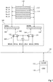
- the figure 1 schematically represents a device, for example an integrated circuit chip, comprising an embodiment of a device 100 for receiving the contents of a memory 110, preferably a memory of the so-called “flash” type, rewritable non-volatile.
- the chip is preferably of the so-called “System on a Chip” or SOC ("System On a Chip”) type.
- SOC type chips are used in particular in embedded or mobile applications, such as mobile telephony, connected objects, household appliances or transport.
- the device 100 is connected, for example connected, to a data bus 120.
- a data processing unit such as a microprocessor 130 (CPU)
- CPU microprocessor
- the bus 120 notably allows the transmission data from memory to the processing unit.
- peripherals not shown, such as sensors, or communication circuits with elements external to the chip, can be connected or connected to the bus 120.
- the link between the device 100 and the bus 120 transmits all the bits in parallel.
- data for example 32 bits.
- the data bus 120 has a size, that is to say a number of bits in parallel, equal to the number of bits of each data.
- the microprocessor 130 comprises, or is connected to, a cache memory 132 (CACHE), or cache memory.
- a cache memory is a memory having for example an access time less than that of the memory 110 and serving as a buffer between the bus 120 and the microprocessor 130.
- the memory 110 comprises a succession of locations 112 and 114.
- the memory locations 112 and 114 follow one another alternately in the order of their addresses, preferably their logical addresses.
- locations 112 and 114 have the same number of bits, preferably 64 bits.
- the addresses are then for example of the form 0x ... 8 for the locations 112, and of the form 0x ... 0 for the locations 114, where "0x" means a hexadecimal notation, and "" represents hexadecimal digits of the address considered.
- the content of each of the locations 112 and 114 corresponds to one or more data.
- each of the locations 112 and 114 contains two data.
- each datum corresponds to 32 bits of low or high weight of the memory location considered.
- the device 100 includes a buffer 102 (BUFA) and a buffer 104 (BUFB).
- buffer is used here to designate a buffer circuit such as a buffer memory, for example a set of flip-flops.
- Each buffer 102, 104 preferably contains the same number of bits as one of the memory locations 112, 114.
- Buffers 102 and 104 can be filled with the respective contents of memory locations 112 and 114.
- buffer 102 is configured or arranged to be filled with the content of a location that can be selected from locations 112.
- buffer 104 is configured or arranged to be filled with the content of a location selectable from locations 114.
- the filling is carried out simultaneously by all the bits of the content of a memory location.
- the filling is then carried out simultaneously with all the data of the content of a memory location.
- the device 100 further comprises a selector 140 for filling mode of the buffers 102 and 104.
- a first filling mode the buffers 102 and 104 are filled simultaneously, that is to say that each buffer 102, 104 is loaded at the same time as the other with the respective content of one of the memory locations 112, 114.
- buffers 102 and 104 are filled sequentially, i.e. during the filling of one of the buffers, the content of the other is left unchanged.
- the selector 140 comprises two multiplexers 152 and 154 controlling the filling of the respective buffers 102 and 104.
- the filling of the buffers 102 and 104 is controlled by respective signals 162 and 164.
- the multiplexers 152 and 154 are controlled by a SEL signal for selecting the filling mode.
- the multiplexers here have inputs I0 and I1 which can be selected according to the high or low state of the multiplexer control signal.
- the inputs I0 and I1, and the low and high levels of the control signals can be exchanged.
- the inputs I1 of the multiplexers 152 and 154 are connected to an application node with the same signal READ_END.
- the inputs I0 of the multiplexers 152 and 154 are for example connected to respective application nodes of different signals READ_ENDA and READ_ENDB.
- the device is preferably configured so that the signals READ_ENDA and READ_ENDB are not emitted simultaneously, as illustrated below.
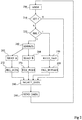
- the figure 2 schematically represents steps of an embodiment of a method implemented by the receiving device 100 of the figure 1 .
- the device 100 receives an ADDR request address, preferably a logical address.
- this address is sent by the microprocessor 130 and / or the cache memory 132 when they need data located in the memory 110 at the request address.
- the ADDR request address can also be issued by any device connected to bus 120, such as a direct memory access device of the DMA ("Direct Memory Access") type.
- the device 100 is preferably connected, for example connected, to an address bus not shown.
- the microprocessor 130 is then connected to the address bus.
- a step 210 (HIT?)
- the device 100 determines whether one of the buffers 102 and 104 already contains the data of the corresponding address in the memory. If this is not the case (output N of block 210), the method goes to step 220.
- step 220 the filling mode is selected between simultaneous filling mode (for example when the SEL signal is at high level '1') and sequential filling mode (for example when the SEL signal is at low level '0 '). If the simultaneous filling mode is selected, the method goes to a step 230. If the sequential filling mode is selected, the method goes to a step 240. The order of steps 210 and 220 can be changed.
- step 230 the contents of locations 112 and 114 are read from memory 110, preferably simultaneously. Preferably, these locations are consecutive and contain the data located at the request address. Preferably, when the reading is finished, an end of reading signal is emitted. This end of reading signal is preferably the READ_END signal for controlling the simultaneous filling of the buffers.
- the method then proceeds to a step 250 (FILL_BUFA & B) of simultaneous filling of the buffers 102 and 104.
- the device 100 selects, between on the one hand the set of locations 112 and on the other hand the set of locations 114, the set which contains the data located at the address of request.
- the device determines for example the fourth bit starting from the least significant (ADDR bit (3), the bits being generally numbered starting from 0). If the ADDR bit (3) is equal to 0, the data contained at the request address is located in one of the locations 112. If the ADDR bit (3) is equal to 1, the data contained at the request address is located in one of the locations 114.
- This example can be adapted for any number of bits of each location 112, 114, for example 32 or 128 bits.
- the content of this location 112 is preferably read in a step 262 (READ_A).
- READ_A an end of reading signal is emitted.
- This signal is preferably the READ_ENDA signal for controlling the filling of the only buffer 102.
- the method proceeds to a step 272 (FILL_BUFA) of filling the buffer 102 with the content of the location 112 considered.
- the content of buffer 104 is left unchanged at this stage.
- the content of this location 114 is preferably read in a step 264 (READ_B).
- READ_B an end of reading signal is emitted.
- This signal is preferably the READ_ENDB signal for controlling the filling of the only buffer 104.
- the method proceeds to a step 274 (FILL_BUFA) of filling the buffer 104 with the content of the location 114 considered. During this time, the content of buffer 102 is not modified.
- step 280 the device 100 determines the position, in buffers 102 and 104, of the data corresponding to the request address. Preferably, four positions are possible: the bits of low weight of buffer 102; the most significant bits of buffer 102; the least significant bits of buffer 104; and the most significant bits of buffer 104.
- a next step 290 the data contained in the buffers 102 and 104 at the position determined in step 280 is sent on the data bus 120.
- the data sent can then be used by the microprocessor 130 and / or the cache memory 132.
- the method preferably resumes at step 200 to receive a new request address.
- step 210 If, at step 210, the data located at the new request address is already in one of the buffers 102 and 104 (output Y of block 210), the method proceeds directly to step 280.
- the signal SEL is modified at a step not shown in the method.
- the loop process thus implemented comprises simultaneous filling of the buffers, and filling of only one of the two buffers and then only the other of the two buffers.
- the method makes it possible to successively send on the bus 120 the data located at various request addresses received in steps 200.
- the locations 112 are located in a first memory bank, and the locations 114 are located in a second memory bank.
- the filling mode selected is sequential filling, for each request address, we read at most one content from only one of the two banks. This reduces energy consumption compared to reading the content of the two banks for each request address.
- the filling mode selected is the simultaneous filling, the two filled buffers make it possible, compared to sequential filling, to save time for example when the processing unit 130 and / or the memory cache 132 need data located at consecutive addresses. It is thus possible to optimize the compromise between the speed of execution and the energy consumption.
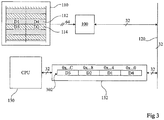
- the figure 3 schematically represents an example of implementation of the method of figure 2 by a chip of the type of that of the figure 1 , when the buffers are filled sequentially.
- the data are 32-bit words
- the data bus 120 is a 32-bit bus
- the locations 112 and 114 of the memory 110 each contain 64 bits
- the cache memory 132 contains locations 302 each containing 128 bit.
- each location 302 of the cache memory can contain four data.
- Each location is for example intended to receive the data located in the memory 110 at respective logical addresses 0x ... 0, 0x ... 4, 0x ... 8, and 0x ... C.
- the microprocessor needs the data located at the logical address 0x ... 4, this data not being present in the cache memory 132. We then fill all of one of the locations 302 of the memory hidden. For this, successive requests are sent to the device 100 so that it successively sends the four corresponding data on the bus 120.
- the first request concerns the address 0x ... 4. This allows the corresponding data D1 to be available as soon as possible for the microprocessor.
- the following requests have successively the addresses 0x ... 8, 0x ... C and 0x..0.
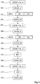
- the figure 4 schematically represents steps of the process of figure 2 in the example of the figure 3 .
- the data D1 located at the request address 0x ... 4 is contained in one of the locations 112.
- This location 112 also contains data D4 located at the address Ox ... 0.
- the method goes through step 262 of reading the content of this location 112 (READ_A), then through step 272 of filling the buffer 102 with this content.
- the buffer 102 then contains the two data D1 and D4.
- the data D1 is sent to the next step 290 (SEND_D1).
- the data D2 located at the request address 0x ... 8 is located in one of the locations 114.
- This location 114 also contains the data D3 located at the address 0x ... C.
- the method goes through step 264 of reading the content of this location 114 (READ_B), then through step 274 of filling the buffer 104 with this content.
- the buffer 104 then contains the two data D2 and D3.
- the data D2 is sent to the next step 290 (SEND_D2).
- step 210 HIT
- step 290 of sending the data item D3 SEND_D3
- step 210 HIT
- step 290 of sending the data D4 SEND_D4.
- the four data D1, D2, D3 and D4 are sent in this order by performing only a step of reading the content of the locations 112 and a step of reading the content of the locations 114. If there was only one the only buffer that can be filled with content from locations 112 and 114, three reading steps would have been necessary.
- the method therefore makes it possible to send contents of the memory faster than with a single buffer.
- we can improve the compromise between speed of execution and energy consumption, compared to a device having an operating mode where two buffers are filled simultaneously and an operating mode where only one of the two buffers can be filled.
- the process is particularly fast for other successions of request addresses than that presented in the example of figures 3 and 4 .
- This advantage exists in particular in the case where the cache memory 132 is omitted and the microprocessor 130 alternately needs data contained in the same location 112 and the same location 114. In this case, once the buffers 102 and 104 are filled, the data is sent on bus 120 without reading the contents of the memory.
- the figure 5 partially and schematically represents a chip comprising an embodiment of a device for receiving the content of memory locations.
- the memory 110 preferably comprises a memory bank 110A (BANKA), in which the locations 112 are located, and a memory bank 110B (BANKB), in which the locations 114 are located.
- BANKA memory bank 110A
- BANKB memory bank 110B
- the bank 110A supplies the content of a memory location to an input I0 of a multiplexer 502.
- the content is supplied after having been selected by its address and read in the memory.
- the bank 110B similarly supplies the content of a memory location to an input I1 of the multiplexer 502.
- the multiplexer 502 is for example controlled by an ADDR signal (3) / 0.
- the ADDR (3) / 0 signal has for example a low level when the simultaneous filling mode is selected.
- the level of the ADDR signal (3) / 0 makes it possible to select the bank which contains the data located at the ADDR request address.
- the signal ADDR (3) / 0 then preferably corresponds to the bit ADDR (3).
- the output of multiplexer 502 is connected to inputs I1 of multiplexers 512, 522 and 524.
- an error correction circuit 532 (ECC) is located between the output of multiplexer 502 and the inputs of multiplexers 512 , 522 and 524.
- the multiplexers 512 and 522 each receive on an input I0 the content of the buffer 102.
- the multiplexer 512 is controlled by the signal READ_END.
- the multiplexer 522 is controlled by the signal READ_ENDA.
- Multiplexer 152 ( figure 1 ) then receives the outputs of the multiplexers 512 and 522.
- the content supplied by the bank 110B is received by an input I1 of a multiplexer 514.
- an error correction circuit 534 (ECC) is located between the output of the bank 110B and the input I1 of the multiplexer 514.
- ECC error correction circuit
- the multiplexers 514 and 524 each receive on an input I0 the content of the buffer 104.
- the multiplexer 514 is controlled by the signal READ_END.
- Multiplexer 524 is controlled by the READ_ENDB signal.
- Multiplexer 154 ( figure 1 ) then receives the outputs of the multiplexers 514 and 524.
- the least significant bits of buffer 102 are connected to an input I00 of a multiplexer 550; the most significant bits of the buffer 102 are connected to an input I01 of the multiplexer 550; the least significant bits of buffer 104 are connected to an input I10 of multiplexer 550; and the most significant bits of the buffer 104 are connected to an input I11 of the multiplexer 550.
- the multiplexer 550 is for example controlled by the ADDR assembly (3: 2) of the third and fourth bits, starting from the least significant, from l 'request address.
- the inputs I00, I01, I10 and I11 are selected according to the respective state '00', '01', '10' and '11' of the ADDR bits (3: 2).
- the output of the multiplexer 550 is connected to the bus 120.
- the links between the banks 110A and 110B, the multiplexers 152, 154, 502, 512, 514, 522 and 524, and the buffers 102 and 104 can transmit all the bits of memory location content in parallel.
- the links between the buffers 102 and 104, the multiplexer 550 and the bus 120 can transmit in parallel all the bits of a data item, preferably 32 bits.
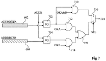
- the figures 6 and 7 schematically represent parts of the receiving device of the figure 5 , allowing the implementation of step 210 (HIT?) of the method of figure 2 .
- the device includes two buffers 602 (ADDRBUFA) and 604 (ADDRBUFB) for storing the request address.
- the request address is received by inputs I1 of multiplexers 612, 614, 622 and 624.
- Multiplexers 612 and 614 receive the content of buffer 602 on inputs I0.
- the outputs of the multiplexers 612 and 614 are connected to the inputs of a multiplexer 632 controlled by the signal SEL.
- Multiplexers 622 and 624 receive the content of buffer 604 on inputs I0.
- the outputs of the multiplexers 622 and 624 are connected to the inputs of a multiplexer 634 controlled by the signal SEL.
- the multiplexers 612 and 622 are controlled respectively by the signals READ_ENDA and READ_ENDB.
- Multiplexers 614 and 624 are controlled together by the signal READ_END.
- the two buffers 602 and 604 are filled with the request address associated with the filling of the buffers 102 and 104 (step 250 of the method of the figure 2 ).
- the buffer 602 or 604 is filled with the request address associated with the filling of the respective buffer 102 or 104 (step 262 or 264).
- the content of the other of the two buffers 602 and 604 is left unchanged.
- the content of buffers 602 and 604 thus corresponds to the request address associated with the filling of buffers 602 and 604.
- the buffer 602 is connected to an input of a circuit 702 (EQ) receiving the request address on another input.
- the circuit 702 is a circuit for verifying equality between the values received on its two inputs. Preferably, the circuit 702 provides a high level when the received values are equal, and a low level when the received values are different.
- the output of circuit 702 is connected to an input of an AND gate 710.
- the AND gate 710 receives an OKA & B signal at another input.
- the output of circuit 702 is also connected to an AND gate 712.
- the AND gate 712 receives an OKA signal at another input.
- Buffer 604 is connected to an input of a circuit 704 (EQ) for checking the equality between two inputs.
- Circuit 704 receives the request address on the other of its two inputs.
- the output of circuit 704 is connected to an input of an AND gate 714.
- the AND gate 714 receives an OKB signal at another input.
- the outputs of AND gates 712 and 714 are connected to the input of an OR gate 720.
- the outputs of OR gate 720 and AND gate 710 are connected to a multiplexer 730.
- Multiplexer 730 is controlled by the signal SEL .
- Multiplexer 730 provides an HIT signal.
- Each of the signals OKA, OKB and OKA & B is activated, for example set to a high level, when validity conditions are met concerning: buffers 102 and 602 for the signal OKA; buffers 104 and 604 for the OKB signal; and these four buffers for the OKA & B signal.
- Such conditions are for example the absence of filling in progress of the buffers concerned, reading in progress of the memory, the presence of a valid datum in the buffers, etc.
- the HIT signal is activated when the data located in the memory at the request address is already in the content of buffers 102 and 104.
- the HIT signal is then used in step 210 (HIT?) Of the method of the figure 2 .
- any circuit making it possible to carry out step 210 of the method of the figure 2 .
- a circuit is configured to memorize in buffers the addresses of the contents filling the buffers. The circuit then determines whether the stored address corresponds to that of a new request.
- step 210 can be omitted.
Landscapes
- Engineering & Computer Science (AREA)
- Theoretical Computer Science (AREA)
- Physics & Mathematics (AREA)
- General Engineering & Computer Science (AREA)
- General Physics & Mathematics (AREA)
- Memory System Of A Hierarchy Structure (AREA)
Applications Claiming Priority (1)
| Application Number | Priority Date | Filing Date | Title |
|---|---|---|---|
| FR1857517A FR3085075A1 (fr) | 2018-08-17 | 2018-08-17 | Controleur memoire |
Publications (2)
| Publication Number | Publication Date |
|---|---|
| EP3611623A1 true EP3611623A1 (de) | 2020-02-19 |
| EP3611623B1 EP3611623B1 (de) | 2023-05-10 |
Family
ID=65201099
Family Applications (1)
| Application Number | Title | Priority Date | Filing Date |
|---|---|---|---|
| EP19188499.8A Active EP3611623B1 (de) | 2018-08-17 | 2019-07-26 | Speichercontroller, der zwei pufferspeicher und eine modusauswahleinheit zur füllung der pufferspeicher enthält |
Country Status (4)
| Country | Link |
|---|---|
| US (1) | US11106582B2 (de) |
| EP (1) | EP3611623B1 (de) |
| CN (2) | CN210072600U (de) |
| FR (1) | FR3085075A1 (de) |
Families Citing this family (2)
| Publication number | Priority date | Publication date | Assignee | Title |
|---|---|---|---|---|
| FR3085075A1 (fr) * | 2018-08-17 | 2020-02-21 | Stmicroelectronics (Grenoble 2) Sas | Controleur memoire |
| CN115244521B (zh) | 2020-05-06 | 2025-07-11 | 阿里巴巴集团控股有限公司 | 用于存储数据的分级方法和系统 |
Citations (1)
| Publication number | Priority date | Publication date | Assignee | Title |
|---|---|---|---|---|
| US20140164713A1 (en) * | 2012-12-09 | 2014-06-12 | Advanced Micro Devices | Bypassing Memory Requests to a Main Memory |
Family Cites Families (9)
| Publication number | Priority date | Publication date | Assignee | Title |
|---|---|---|---|---|
| US5163132A (en) * | 1987-09-24 | 1992-11-10 | Ncr Corporation | Integrated controller using alternately filled and emptied buffers for controlling bi-directional data transfer between a processor and a data storage device |
| GB2222471B (en) * | 1988-08-29 | 1992-12-09 | Mitsubishi Electric Corp | Ic card with switchable bus structure |
| JP4435802B2 (ja) * | 2007-04-11 | 2010-03-24 | 株式会社日立ハイテクノロジーズ | 半導体検査装置 |
| US20120066444A1 (en) * | 2010-09-14 | 2012-03-15 | Advanced Micro Devices, Inc. | Resolution Enhancement of Video Stream Based on Spatial and Temporal Correlation |
| US10339079B2 (en) * | 2014-06-02 | 2019-07-02 | Western Digital Technologies, Inc. | System and method of interleaving data retrieved from first and second buffers |
| US9792965B2 (en) * | 2014-06-17 | 2017-10-17 | Rambus Inc. | Memory module and system supporting parallel and serial access modes |
| US10678459B2 (en) * | 2015-08-06 | 2020-06-09 | Rambus Inc. | High performance, high capacity memory modules and systems |
| FR3085075A1 (fr) * | 2018-08-17 | 2020-02-21 | Stmicroelectronics (Grenoble 2) Sas | Controleur memoire |
| US11048649B2 (en) * | 2018-10-17 | 2021-06-29 | Macronix International Co., Ltd. | Non-sequential page continuous read |
-
2018
- 2018-08-17 FR FR1857517A patent/FR3085075A1/fr not_active Ceased
-
2019
- 2019-07-26 EP EP19188499.8A patent/EP3611623B1/de active Active
- 2019-08-02 US US16/530,049 patent/US11106582B2/en active Active
- 2019-08-16 CN CN201921332849.3U patent/CN210072600U/zh active Active
- 2019-08-16 CN CN201910758944.8A patent/CN110837481B/zh active Active
Patent Citations (1)
| Publication number | Priority date | Publication date | Assignee | Title |
|---|---|---|---|---|
| US20140164713A1 (en) * | 2012-12-09 | 2014-06-12 | Advanced Micro Devices | Bypassing Memory Requests to a Main Memory |
Non-Patent Citations (3)
| Title |
|---|
| HUSSAIN TASSADAQ ED - MCINTOSH-SMITH SIMON ET AL: "A novel hardware support for heterogeneous multi-core memory system", JOURNAL OF PARALLEL AND DISTRIBUTED COMPUTING, ELSEVIER, AMSTERDAM, NL, vol. 106, 16 March 2017 (2017-03-16), pages 31 - 49, XP085008765, ISSN: 0743-7315, DOI: 10.1016/J.JPDC.2017.02.008 * |
| NIMA HONARMAND: "Main memory and DRAM", 2015, pages 1 - 37, XP002791157, Retrieved from the Internet <URL:https://compas.cs.stonybrook.edu/~nhonarmand/courses/sp15/cse502/slides/06-main_mem.pdf> [retrieved on 20190510] * |
| PARK JAEHYUN ET AL: "Prefetch-based dynamic row buffer management for LPDDR2-NVM devices", 2015 IFIP/IEEE INTERNATIONAL CONFERENCE ON VERY LARGE SCALE INTEGRATION (VLSI-SOC), IEEE, 5 October 2015 (2015-10-05), pages 98 - 103, XP032803865, DOI: 10.1109/VLSI-SOC.2015.7314399 * |
Also Published As
| Publication number | Publication date |
|---|---|
| US20200057719A1 (en) | 2020-02-20 |
| CN210072600U (zh) | 2020-02-14 |
| CN110837481A (zh) | 2020-02-25 |
| FR3085075A1 (fr) | 2020-02-21 |
| EP3611623B1 (de) | 2023-05-10 |
| CN110837481B (zh) | 2025-04-04 |
| US11106582B2 (en) | 2021-08-31 |
Similar Documents
| Publication | Publication Date | Title |
|---|---|---|
| FR2667706A1 (fr) | Antememoire hierarchique a circuits integres. | |
| FR2844613A1 (fr) | Systeme pour le transfert rapide des donnees | |
| EP0558125B1 (de) | Neuronaler Prozessor mit verteilten synaptischen Zellen | |
| FR2602070A1 (fr) | Systeme et procede d'acces a une memoire d'ordinateur. | |
| FR2624994A1 (fr) | Systeme de commande de registre intermediaire de traduction | |
| FR2674654A1 (fr) | Systeme de commande de registres partages. | |
| EP0439855B1 (de) | Mikrokontroller zur schnellen Ausführung einer grossen Anzahl von Befehlen, die in Folgen von gleichartigen Befehlen zerlegbar sind | |
| EP1668530A2 (de) | Komponente mit dynamisch umkonfigurierbarer architektur | |
| FR2664719A1 (fr) | Dispositif de controle pour une memoire tampon a partitionnement reconfigurable. | |
| EP0020983A1 (de) | Speichersystem mit einer serienmässigen Speichervorrichtung | |
| EP3611623B1 (de) | Speichercontroller, der zwei pufferspeicher und eine modusauswahleinheit zur füllung der pufferspeicher enthält | |
| FR2486290A1 (fr) | Dispositif de transmission rapide de donnees comportant un circuit de commande a acces direct a la memoire | |
| FR3042050B1 (fr) | Dispositif informatique muni de traitement en memoire et de ports d'acces etroits | |
| FR2634919A1 (fr) | Interface de bus pour microprocesseur | |
| FR2513410A1 (fr) | Microprocesseur et procede pour imbriquer les acces en memoire de ce microprocesseur | |
| EP0392932B1 (de) | Verfahren und Vorrichtung zur Speicherzugriffsbeschleunigung unter Verwendung eines modifizierten LRU-Algorithmus | |
| EP0920157A1 (de) | Verwaltungseinrichtung eines gemeinsamen Pufferspeichers | |
| FR2472232A1 (fr) | Dispositif et procede d'effacement d'antememoire | |
| EP0677934B1 (de) | Verfahren zur Mustererkennung in einer seriellen Übertragung | |
| FR2536884A1 (fr) | Reseau de transfert de donnees entre plusieurs processeurs et une memoire | |
| EP0251861B1 (de) | Speicherverwaltungseinheit | |
| EP3667503A1 (de) | Verwaltungsverfahren des speicherplatzes einer speichervorrichtung und entsprechendes system | |
| EP1248261A2 (de) | Random und schnelles DRAM Speicher Direktzugriffmanagementsverfahren | |
| FR3041796A1 (fr) | Stockage et lecture d'un code d'authentification de message dans une memoire externe | |
| FR2801388A1 (fr) | Procede de commande de memoire dram rapide et controleur adapte |
Legal Events
| Date | Code | Title | Description |
|---|---|---|---|
| PUAI | Public reference made under article 153(3) epc to a published international application that has entered the european phase |
Free format text: ORIGINAL CODE: 0009012 |
|
| STAA | Information on the status of an ep patent application or granted ep patent |
Free format text: STATUS: REQUEST FOR EXAMINATION WAS MADE |
|
| 17P | Request for examination filed |
Effective date: 20190726 |
|
| AK | Designated contracting states |
Kind code of ref document: A1 Designated state(s): AL AT BE BG CH CY CZ DE DK EE ES FI FR GB GR HR HU IE IS IT LI LT LU LV MC MK MT NL NO PL PT RO RS SE SI SK SM TR |
|
| AX | Request for extension of the european patent |
Extension state: BA ME |
|
| STAA | Information on the status of an ep patent application or granted ep patent |
Free format text: STATUS: EXAMINATION IS IN PROGRESS |
|
| 17Q | First examination report despatched |
Effective date: 20210504 |
|
| RIC1 | Information provided on ipc code assigned before grant |
Ipc: G06F 12/0862 20160101ALN20220812BHEP Ipc: G06F 13/16 20060101ALI20220812BHEP Ipc: G06F 12/06 20060101ALI20220812BHEP Ipc: G06F 12/02 20060101AFI20220812BHEP |
|
| RIC1 | Information provided on ipc code assigned before grant |
Ipc: G06F 12/0862 20160101ALN20220922BHEP Ipc: G06F 13/16 20060101ALI20220922BHEP Ipc: G06F 12/06 20060101ALI20220922BHEP Ipc: G06F 12/02 20060101AFI20220922BHEP |
|
| GRAP | Despatch of communication of intention to grant a patent |
Free format text: ORIGINAL CODE: EPIDOSNIGR1 |
|
| STAA | Information on the status of an ep patent application or granted ep patent |
Free format text: STATUS: GRANT OF PATENT IS INTENDED |
|
| INTG | Intention to grant announced |
Effective date: 20221110 |
|
| GRAJ | Information related to disapproval of communication of intention to grant by the applicant or resumption of examination proceedings by the epo deleted |
Free format text: ORIGINAL CODE: EPIDOSDIGR1 |
|
| STAA | Information on the status of an ep patent application or granted ep patent |
Free format text: STATUS: EXAMINATION IS IN PROGRESS |
|
| GRAP | Despatch of communication of intention to grant a patent |
Free format text: ORIGINAL CODE: EPIDOSNIGR1 |
|
| STAA | Information on the status of an ep patent application or granted ep patent |
Free format text: STATUS: GRANT OF PATENT IS INTENDED |
|
| INTC | Intention to grant announced (deleted) | ||
| GRAS | Grant fee paid |
Free format text: ORIGINAL CODE: EPIDOSNIGR3 |
|
| GRAA | (expected) grant |
Free format text: ORIGINAL CODE: 0009210 |
|
| STAA | Information on the status of an ep patent application or granted ep patent |
Free format text: STATUS: THE PATENT HAS BEEN GRANTED |
|
| RIC1 | Information provided on ipc code assigned before grant |
Ipc: G06F 12/0862 20160101ALN20230308BHEP Ipc: G06F 13/16 20060101ALI20230308BHEP Ipc: G06F 12/06 20060101ALI20230308BHEP Ipc: G06F 12/02 20060101AFI20230308BHEP |
|
| INTG | Intention to grant announced |
Effective date: 20230322 |
|
| AK | Designated contracting states |
Kind code of ref document: B1 Designated state(s): AL AT BE BG CH CY CZ DE DK EE ES FI FR GB GR HR HU IE IS IT LI LT LU LV MC MK MT NL NO PL PT RO RS SE SI SK SM TR |
|
| REG | Reference to a national code |
Ref country code: GB Ref legal event code: FG4D Free format text: NOT ENGLISH |
|
| REG | Reference to a national code |
Ref country code: AT Ref legal event code: REF Ref document number: 1567396 Country of ref document: AT Kind code of ref document: T Effective date: 20230515 Ref country code: CH Ref legal event code: EP |
|
| REG | Reference to a national code |
Ref country code: DE Ref legal event code: R096 Ref document number: 602019028622 Country of ref document: DE |
|
| REG | Reference to a national code |
Ref country code: IE Ref legal event code: FG4D Free format text: LANGUAGE OF EP DOCUMENT: FRENCH |
|
| REG | Reference to a national code |
Ref country code: LT Ref legal event code: MG9D |
|
| REG | Reference to a national code |
Ref country code: NL Ref legal event code: MP Effective date: 20230510 |
|
| REG | Reference to a national code |
Ref country code: AT Ref legal event code: MK05 Ref document number: 1567396 Country of ref document: AT Kind code of ref document: T Effective date: 20230510 |
|
| PG25 | Lapsed in a contracting state [announced via postgrant information from national office to epo] |
Ref country code: SE Free format text: LAPSE BECAUSE OF FAILURE TO SUBMIT A TRANSLATION OF THE DESCRIPTION OR TO PAY THE FEE WITHIN THE PRESCRIBED TIME-LIMIT Effective date: 20230510 Ref country code: PT Free format text: LAPSE BECAUSE OF FAILURE TO SUBMIT A TRANSLATION OF THE DESCRIPTION OR TO PAY THE FEE WITHIN THE PRESCRIBED TIME-LIMIT Effective date: 20230911 Ref country code: NO Free format text: LAPSE BECAUSE OF FAILURE TO SUBMIT A TRANSLATION OF THE DESCRIPTION OR TO PAY THE FEE WITHIN THE PRESCRIBED TIME-LIMIT Effective date: 20230810 Ref country code: NL Free format text: LAPSE BECAUSE OF FAILURE TO SUBMIT A TRANSLATION OF THE DESCRIPTION OR TO PAY THE FEE WITHIN THE PRESCRIBED TIME-LIMIT Effective date: 20230510 Ref country code: ES Free format text: LAPSE BECAUSE OF FAILURE TO SUBMIT A TRANSLATION OF THE DESCRIPTION OR TO PAY THE FEE WITHIN THE PRESCRIBED TIME-LIMIT Effective date: 20230510 Ref country code: AT Free format text: LAPSE BECAUSE OF FAILURE TO SUBMIT A TRANSLATION OF THE DESCRIPTION OR TO PAY THE FEE WITHIN THE PRESCRIBED TIME-LIMIT Effective date: 20230510 |
|
| PG25 | Lapsed in a contracting state [announced via postgrant information from national office to epo] |
Ref country code: RS Free format text: LAPSE BECAUSE OF FAILURE TO SUBMIT A TRANSLATION OF THE DESCRIPTION OR TO PAY THE FEE WITHIN THE PRESCRIBED TIME-LIMIT Effective date: 20230510 Ref country code: PL Free format text: LAPSE BECAUSE OF FAILURE TO SUBMIT A TRANSLATION OF THE DESCRIPTION OR TO PAY THE FEE WITHIN THE PRESCRIBED TIME-LIMIT Effective date: 20230510 Ref country code: LV Free format text: LAPSE BECAUSE OF FAILURE TO SUBMIT A TRANSLATION OF THE DESCRIPTION OR TO PAY THE FEE WITHIN THE PRESCRIBED TIME-LIMIT Effective date: 20230510 Ref country code: LT Free format text: LAPSE BECAUSE OF FAILURE TO SUBMIT A TRANSLATION OF THE DESCRIPTION OR TO PAY THE FEE WITHIN THE PRESCRIBED TIME-LIMIT Effective date: 20230510 Ref country code: IS Free format text: LAPSE BECAUSE OF FAILURE TO SUBMIT A TRANSLATION OF THE DESCRIPTION OR TO PAY THE FEE WITHIN THE PRESCRIBED TIME-LIMIT Effective date: 20230910 Ref country code: HR Free format text: LAPSE BECAUSE OF FAILURE TO SUBMIT A TRANSLATION OF THE DESCRIPTION OR TO PAY THE FEE WITHIN THE PRESCRIBED TIME-LIMIT Effective date: 20230510 Ref country code: GR Free format text: LAPSE BECAUSE OF FAILURE TO SUBMIT A TRANSLATION OF THE DESCRIPTION OR TO PAY THE FEE WITHIN THE PRESCRIBED TIME-LIMIT Effective date: 20230811 |
|
| PG25 | Lapsed in a contracting state [announced via postgrant information from national office to epo] |
Ref country code: FI Free format text: LAPSE BECAUSE OF FAILURE TO SUBMIT A TRANSLATION OF THE DESCRIPTION OR TO PAY THE FEE WITHIN THE PRESCRIBED TIME-LIMIT Effective date: 20230510 |
|
| PG25 | Lapsed in a contracting state [announced via postgrant information from national office to epo] |
Ref country code: SK Free format text: LAPSE BECAUSE OF FAILURE TO SUBMIT A TRANSLATION OF THE DESCRIPTION OR TO PAY THE FEE WITHIN THE PRESCRIBED TIME-LIMIT Effective date: 20230510 |
|
| PG25 | Lapsed in a contracting state [announced via postgrant information from national office to epo] |
Ref country code: SM Free format text: LAPSE BECAUSE OF FAILURE TO SUBMIT A TRANSLATION OF THE DESCRIPTION OR TO PAY THE FEE WITHIN THE PRESCRIBED TIME-LIMIT Effective date: 20230510 Ref country code: SK Free format text: LAPSE BECAUSE OF FAILURE TO SUBMIT A TRANSLATION OF THE DESCRIPTION OR TO PAY THE FEE WITHIN THE PRESCRIBED TIME-LIMIT Effective date: 20230510 Ref country code: RO Free format text: LAPSE BECAUSE OF FAILURE TO SUBMIT A TRANSLATION OF THE DESCRIPTION OR TO PAY THE FEE WITHIN THE PRESCRIBED TIME-LIMIT Effective date: 20230510 Ref country code: EE Free format text: LAPSE BECAUSE OF FAILURE TO SUBMIT A TRANSLATION OF THE DESCRIPTION OR TO PAY THE FEE WITHIN THE PRESCRIBED TIME-LIMIT Effective date: 20230510 Ref country code: DK Free format text: LAPSE BECAUSE OF FAILURE TO SUBMIT A TRANSLATION OF THE DESCRIPTION OR TO PAY THE FEE WITHIN THE PRESCRIBED TIME-LIMIT Effective date: 20230510 Ref country code: CZ Free format text: LAPSE BECAUSE OF FAILURE TO SUBMIT A TRANSLATION OF THE DESCRIPTION OR TO PAY THE FEE WITHIN THE PRESCRIBED TIME-LIMIT Effective date: 20230510 |
|
| REG | Reference to a national code |
Ref country code: DE Ref legal event code: R097 Ref document number: 602019028622 Country of ref document: DE |
|
| PG25 | Lapsed in a contracting state [announced via postgrant information from national office to epo] |
Ref country code: MC Free format text: LAPSE BECAUSE OF FAILURE TO SUBMIT A TRANSLATION OF THE DESCRIPTION OR TO PAY THE FEE WITHIN THE PRESCRIBED TIME-LIMIT Effective date: 20230510 |
|
| PG25 | Lapsed in a contracting state [announced via postgrant information from national office to epo] |
Ref country code: MC Free format text: LAPSE BECAUSE OF FAILURE TO SUBMIT A TRANSLATION OF THE DESCRIPTION OR TO PAY THE FEE WITHIN THE PRESCRIBED TIME-LIMIT Effective date: 20230510 |
|
| REG | Reference to a national code |
Ref country code: CH Ref legal event code: PL |
|
| PLBE | No opposition filed within time limit |
Free format text: ORIGINAL CODE: 0009261 |
|
| STAA | Information on the status of an ep patent application or granted ep patent |
Free format text: STATUS: NO OPPOSITION FILED WITHIN TIME LIMIT |
|
| REG | Reference to a national code |
Ref country code: BE Ref legal event code: MM Effective date: 20230731 |
|
| PG25 | Lapsed in a contracting state [announced via postgrant information from national office to epo] |
Ref country code: LU Free format text: LAPSE BECAUSE OF NON-PAYMENT OF DUE FEES Effective date: 20230726 |
|
| PG25 | Lapsed in a contracting state [announced via postgrant information from national office to epo] |
Ref country code: LU Free format text: LAPSE BECAUSE OF NON-PAYMENT OF DUE FEES Effective date: 20230726 |
|
| 26N | No opposition filed |
Effective date: 20240213 |
|
| GBPC | Gb: european patent ceased through non-payment of renewal fee |
Effective date: 20230810 |
|
| REG | Reference to a national code |
Ref country code: IE Ref legal event code: MM4A |
|
| PG25 | Lapsed in a contracting state [announced via postgrant information from national office to epo] |
Ref country code: CH Free format text: LAPSE BECAUSE OF NON-PAYMENT OF DUE FEES Effective date: 20230731 |
|
| PG25 | Lapsed in a contracting state [announced via postgrant information from national office to epo] |
Ref country code: SI Free format text: LAPSE BECAUSE OF FAILURE TO SUBMIT A TRANSLATION OF THE DESCRIPTION OR TO PAY THE FEE WITHIN THE PRESCRIBED TIME-LIMIT Effective date: 20230510 |
|
| PG25 | Lapsed in a contracting state [announced via postgrant information from national office to epo] |
Ref country code: SI Free format text: LAPSE BECAUSE OF FAILURE TO SUBMIT A TRANSLATION OF THE DESCRIPTION OR TO PAY THE FEE WITHIN THE PRESCRIBED TIME-LIMIT Effective date: 20230510 Ref country code: IT Free format text: LAPSE BECAUSE OF FAILURE TO SUBMIT A TRANSLATION OF THE DESCRIPTION OR TO PAY THE FEE WITHIN THE PRESCRIBED TIME-LIMIT Effective date: 20230510 Ref country code: FR Free format text: LAPSE BECAUSE OF NON-PAYMENT OF DUE FEES Effective date: 20230731 Ref country code: BE Free format text: LAPSE BECAUSE OF NON-PAYMENT OF DUE FEES Effective date: 20230731 |
|
| PG25 | Lapsed in a contracting state [announced via postgrant information from national office to epo] |
Ref country code: IE Free format text: LAPSE BECAUSE OF NON-PAYMENT OF DUE FEES Effective date: 20230726 |
|
| PG25 | Lapsed in a contracting state [announced via postgrant information from national office to epo] |
Ref country code: GB Free format text: LAPSE BECAUSE OF NON-PAYMENT OF DUE FEES Effective date: 20230810 |
|
| PG25 | Lapsed in a contracting state [announced via postgrant information from national office to epo] |
Ref country code: IE Free format text: LAPSE BECAUSE OF NON-PAYMENT OF DUE FEES Effective date: 20230726 Ref country code: GB Free format text: LAPSE BECAUSE OF NON-PAYMENT OF DUE FEES Effective date: 20230810 |
|
| PG25 | Lapsed in a contracting state [announced via postgrant information from national office to epo] |
Ref country code: BG Free format text: LAPSE BECAUSE OF FAILURE TO SUBMIT A TRANSLATION OF THE DESCRIPTION OR TO PAY THE FEE WITHIN THE PRESCRIBED TIME-LIMIT Effective date: 20230510 |
|
| PG25 | Lapsed in a contracting state [announced via postgrant information from national office to epo] |
Ref country code: BG Free format text: LAPSE BECAUSE OF FAILURE TO SUBMIT A TRANSLATION OF THE DESCRIPTION OR TO PAY THE FEE WITHIN THE PRESCRIBED TIME-LIMIT Effective date: 20230510 |
|
| PG25 | Lapsed in a contracting state [announced via postgrant information from national office to epo] |
Ref country code: CY Free format text: LAPSE BECAUSE OF FAILURE TO SUBMIT A TRANSLATION OF THE DESCRIPTION OR TO PAY THE FEE WITHIN THE PRESCRIBED TIME-LIMIT; INVALID AB INITIO Effective date: 20190726 |
|
| PG25 | Lapsed in a contracting state [announced via postgrant information from national office to epo] |
Ref country code: HU Free format text: LAPSE BECAUSE OF FAILURE TO SUBMIT A TRANSLATION OF THE DESCRIPTION OR TO PAY THE FEE WITHIN THE PRESCRIBED TIME-LIMIT; INVALID AB INITIO Effective date: 20190726 |
|
| PGFP | Annual fee paid to national office [announced via postgrant information from national office to epo] |
Ref country code: DE Payment date: 20250620 Year of fee payment: 7 |
|
| PG25 | Lapsed in a contracting state [announced via postgrant information from national office to epo] |
Ref country code: TR Free format text: LAPSE BECAUSE OF FAILURE TO SUBMIT A TRANSLATION OF THE DESCRIPTION OR TO PAY THE FEE WITHIN THE PRESCRIBED TIME-LIMIT Effective date: 20230510 |