EP3612877B1 - Jonction de guide d'ondes planaire - Google Patents
Jonction de guide d'ondes planaire Download PDFInfo
- Publication number
- EP3612877B1 EP3612877B1 EP18787064.7A EP18787064A EP3612877B1 EP 3612877 B1 EP3612877 B1 EP 3612877B1 EP 18787064 A EP18787064 A EP 18787064A EP 3612877 B1 EP3612877 B1 EP 3612877B1
- Authority
- EP
- European Patent Office
- Prior art keywords
- waveguide
- section
- segments
- optical
- profile
- Prior art date
- Legal status (The legal status is an assumption and is not a legal conclusion. Google has not performed a legal analysis and makes no representation as to the accuracy of the status listed.)
- Active
Links
Images





Classifications
-
- G—PHYSICS
- G02—OPTICS
- G02B—OPTICAL ELEMENTS, SYSTEMS OR APPARATUS
- G02B6/00—Light guides; Structural details of arrangements comprising light guides and other optical elements, e.g. couplings
- G02B6/10—Light guides; Structural details of arrangements comprising light guides and other optical elements, e.g. couplings of the optical waveguide type
- G02B6/12—Light guides; Structural details of arrangements comprising light guides and other optical elements, e.g. couplings of the optical waveguide type of the integrated circuit kind
- G02B6/122—Basic optical elements, e.g. light-guiding paths
- G02B6/125—Bends, branchings or intersections
-
- G—PHYSICS
- G02—OPTICS
- G02B—OPTICAL ELEMENTS, SYSTEMS OR APPARATUS
- G02B6/00—Light guides; Structural details of arrangements comprising light guides and other optical elements, e.g. couplings
- G02B6/10—Light guides; Structural details of arrangements comprising light guides and other optical elements, e.g. couplings of the optical waveguide type
- G02B6/12—Light guides; Structural details of arrangements comprising light guides and other optical elements, e.g. couplings of the optical waveguide type of the integrated circuit kind
- G02B6/122—Basic optical elements, e.g. light-guiding paths
- G02B6/1228—Tapered waveguides, e.g. integrated spot-size transformers
-
- G—PHYSICS
- G02—OPTICS
- G02B—OPTICAL ELEMENTS, SYSTEMS OR APPARATUS
- G02B6/00—Light guides; Structural details of arrangements comprising light guides and other optical elements, e.g. couplings
- G02B6/10—Light guides; Structural details of arrangements comprising light guides and other optical elements, e.g. couplings of the optical waveguide type
- G02B6/12—Light guides; Structural details of arrangements comprising light guides and other optical elements, e.g. couplings of the optical waveguide type of the integrated circuit kind
- G02B6/126—Light guides; Structural details of arrangements comprising light guides and other optical elements, e.g. couplings of the optical waveguide type of the integrated circuit kind using polarisation effects
-
- G—PHYSICS
- G02—OPTICS
- G02B—OPTICAL ELEMENTS, SYSTEMS OR APPARATUS
- G02B6/00—Light guides; Structural details of arrangements comprising light guides and other optical elements, e.g. couplings
- G02B6/10—Light guides; Structural details of arrangements comprising light guides and other optical elements, e.g. couplings of the optical waveguide type
- G02B6/12—Light guides; Structural details of arrangements comprising light guides and other optical elements, e.g. couplings of the optical waveguide type of the integrated circuit kind
- G02B2006/12133—Functions
- G02B2006/1215—Splitter
Definitions
- This invention relates to low optical loss passive optical coupler/splitter for a planar lightwave circuit.
- the invention further relates to methods for forming planar lightwave circuits comprising low loss optical couplers.
- Planar Lightwave Circuit (PLC) technology has become the dominant technology platform for the integration of existing and new optical-assembly functions into chip-based silica-waveguide integrated optical circuits (see, for example, K. Okamoto (2010), “Fundamentals of Optical Waveguides” (Academic Press ) as basics of optical waveguide technology and formation of planar lightwave circuits).
- Y-Branch waveguides are an important integrated-optic circuit element in a broad range of optical circuits. Y-Branch waveguides are used to distribute the optical signal from a single waveguide into two separate waveguides (a 'splitter'); or to recombine two optical signals (according to interference principles) that have propagated along separate paths (a 'combiner'). This 1x2 nature of the Y-Branch waveguide is expanded to greater splitting or combining ratios by integrated cascading of Y-Branch circuit elements.
- Optical waveguides do not 'contain' the propagation of optical signals as wires contain the propagation of electrical signals. Waveguides merely influence the propagation of optical signals along or nearby their paths. Imperfections in the waveguide structure generally result in some of the light of the optical signal merely propagating away from the waveguides. This results in a reduction of energy in the guided optical signals and diminished signal integrity. It is therefore a significant design objective of such waveguide circuit elements that they have as little excess loss as possible. Since Y-Branch elements are often cascaded to generate larger manifolds, even a small percentage of loss in each Y-Branch can lead to undesirable circuit loss.
- Optical networks generally comprise transmission components that are designed to transmit bands of wavelengths over reasonable distances.
- the bands of wavelengths generally comprise signals intended for a plurality of customers/users.
- a single optical fiber can be used to simultaneously transmit a plurality of signals that are subsequently divided for delivery.
- individual signals are combined for transmission over common lines prior to eventual division for routing and/or delivery.
- Individual bands thus are divided into smaller wavelength ranges corresponding to signals relating to individual users, including aggregations of a few users, and multiplexing and de-multiplexing functions can be used to convert between combined signals for common lines and individual signals for routing and/or interfacing with individual users.
- Planar lightwave circuits are generally used effectively for many optical functions used for wavelength division multiplexing.
- the present invention provides a planar waveguide junction with the features of claim 1.
- an optical mixer comprising a) a curved waveguide comprising an input waveguide section, a coupling section and a terminating section; and b) a Y-splitter positioned to optically couple to the curved waveguide at the coupling section.
- the Y-splitter can comprise an input waveguide section, a transition section, a first output section and a second output section, in which the transition section optically connects the input waveguide section with the first output waveguide section and the second output waveguide section.
- the input section comprises a taper from an initial width of w to a tapered with of 2w+g.
- the taper can be configured for optical coupling with the curved waveguide such that a zero order mode in the curved waveguide couples into a first order mode in the input waveguide section, and wherein the transition section comprises alternating gapped segments and ungapped segments along the optical path, the gapped segments having transverse to the optical path waveguide cores corresponding to the two output waveguide sections separated by gaps in the optical core, and the ungapped segments having transverse continuous core.
- the optical mixer can be used in method for controlling optical signal output, in which the method comprises combining two optical signals and directing the combined optical signal into the transition region to direct selected optical signals into the first output section and the second output section based on the phase relationship of the two optical signals.
- a first optical signal is in a zero order mode and a second optical signal is in a first order mode to provide for interference of the two optical signals within the input section of the Y-splitter to form the combined optical signal.
- the method can be used to achieve variable optical attenuation, optical switching, or polarization beam splitting.
- a first polarization of the first optical signal arrives at the mixer 180 degrees out of phase with respect to the corresponding polarization of the second optical signal
- a second polarization of the first optical signal arrives at the mixer in-phase with respect to the corresponding polarization of the second optical signal.
- the invention pertains to the planar waveguide junction according to claim 1 being an asymmetric optical junction, in which the first output waveguide section has a width perpendicular to the optical path at the transition section that is at least about 10% greater than the corresponding width of the second output section.
- Optical couplers with improved performance are described having a transition section connecting N input waveguide sections with M output waveguide sections that decreases optical loss resulting from non-ideal behavior around the junction joining the branched waveguides.
- the English-language definition of 'waggle' includes "to move side to side in a short, rapid manner".
- the two (or more) separate waveguides shift side-to-side in and out over a relatively short propagation distance covering a transition region.
- the transition region spans between a first waveguide structure, such as a single broadened waveguide, and a second waveguide structure, such as a two split waveguides, although alternative transitions are further described below.
- Resulting structures are found to have lower amounts of optical loss resulting from the splitting of an input waveguide into output waveguides.
- a corresponding waggled transition can be used for an asymmetric transition, a 1 ⁇ 3 transition, a 2 x 3 transition or other transitions.
- the waggled transitions are found to be particularly effective for forming optical taps.
- the splitters/couplers can be integrated into a planar lightwave circuit (PLC) alone or with additional optical components. PLC processing technology to form the structures are described.
- splitters/couplers described herein are applicable across a very broad range of waveguide parameters.
- a representative example would be: (i) refractive index of the core 1.5% higher than the surrounding material; (ii) waveguide thickness is roughly 4 microns; (iii) nominal waveguide width (before taper, or after split) is roughly 4 microns; and (iv) minimum formable gap between waveguides of roughly 2 microns.
- these example parameters which are suitable for silica glass waveguides, are used throughout for discussions, configurations, and simulations, although the devices based on the teachings herein are not limited to these example parameters.
- a person of ordinary skill in the art can scale the structures accordingly for different suitable parameters, such as a higher index of refraction difference, different waveguide dimensions for different optical frequencies, different optical materials, or other design issues known in the art.
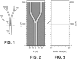
- FIG. 1 An idealized Y-branch splitter 100 is depicted in Fig. 1 .
- the physical layout of the ideal splitter in Fig. 1 is not to scale as the length along the propagation direction (vertical in the figure) would be much longer than depicted compared to the transverse width (horizontal in the figure).
- Idealized Y-branch splitter 100 comprises a single waveguide section 102, transition waveguide section 104, first split waveguide section 106 and second split waveguide section 108.
- a single waveguide section starting at the bottom gradually widens to about twice its width, then splits into two waveguide sections that gradually separate for some distance, then separate more quickly after the two waveguides have become sufficiently independent.
- transition waveguide section 104 at the split waveguide end can be selected based on the optical properties and does not need to be precisely defined. But once the optical signals are localized in the split waveguides, the waveguides are appropriately considered as the split waveguides. This configuration closely resembles the letter 'Y', and hence is commonly referred to as a Y-Branch splitter (or combiner).
- Fig. 2 shows the numerical simulation of optical propagation through the ideal Y-branch structure of Fig. 1 from bottom to top in the orientation depicted in the figure. This simulation and the correspondingly similar simulations provided herein are based on the well-known "beam propagation method" (BPM).
- Fig. 2 shows the electric field intensity which is shown to be concentrated along the core of the waveguide with the signal smoothly transitioning into the split waveguides along the transition region. This shows that the ideal Y-Branch efficiently and equally divides the optical power into the two branches.
- the plot of Fig. 3 shows the calculated fraction of the input power (normalized to 1) coupled into the individual output waveguides from the numerical simulation.
- the value is zero before the split because there are no output waveguides there.
- the output waveguide sections first start to split, there is not a distinct separation between them and for a short distance the power cannot be calculated accurately. Therefore, the measured power temporarily exceeds the 0.5 (50%) maximum power for each waveguide. As the waveguides more distinctly separate, the power measurements accurately reflect what is being simulated.
- the split waveguides are identifiable, the light intensity in each output arm of the ideal splitter is essentially equal to the 50% theoretical maximum, hence the identification of the splitter as 'ideal'.
- PLC technology has become the dominant commercial technology for passive integrated optics, but using practical fabrication techniques, PLC technology is not capable of making an ideal splitter as depicted in Fig. 1 .
- the waveguide is a 3-dimensional structure that is approximately as deep as it is wide. As such, it is not possible to accurately create the deep, narrow gap sharply tapering between the waveguides where they first start to separate.
- PLC waveguide design using practical fabrication techniques requires a 'minimum gap' between waveguides, so in the Y-branch, the single waveguide must further expand until it is as wide as both output waveguides plus the minimum gap before the output waveguides can begin.
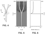
- a practical Y-branch splitter 120 adapted from the ideal splitter is depicted in Fig.
- Y-branch splitter 120 comprises input waveguide section 122, transition waveguide section 124, first split waveguide segment 126 and second split waveguide section 128.
- the transition waveguide section has an edge marked on the side of input waveguide section 122 at a point where the width is 2 w, where w is the nominal long distance waveguide width. Again, the edge of transition waveguide section 124 toward the split waveguide sections is not particularly significant except that once the signals are well localized in the individual waveguides it is appropriate to consider the waveguides as split.
- the finite gap is marked "g" in Fig. 4 .
- Fig. 5 depicts the electric field intensity from a BPM simulation of optical propagation through the structure of Fig. 4 according to the example parameters above. From Fig. 5 , it can be readily seen that the optical propagation is notably disrupted by the finite gap, g. This observation is confirmed in Fig. 6 showing the fraction of the normalized light input power that substantially less than the ideal 50% is coupled into each of the output waveguides, the rest being lost into the surrounding medium.
- Fig. 7 shows the waveguide layout for a Y-branch splitter 140 in the spirit of the improvements suggested in US-A-5,745,618 and others, adding progressively thinner bridges 142 of core material forming a transition waveguide section 144 from an input waveguide section 146 to the diverging waveguides 148, 150. Referring back to Fig.
- Sakamaki et al. suggests a computer-optimized multiple random variations of waveguide width along the lower arm in order to yield a splitting of the central peak (see, Sakamaki et al., "Low-Loss Y-Branch Waveguides Designed by Wavefront Matching Method," Journal of Lightwave Technology, 27(9) May 2009, pp1128-1134 ).
- the wavefront matching approach of Sakamaki et al. is certainly promising in principle, but require a delicate balancing of design parameters and present significant challenges in faithfully translating those balanced numerical designs into practically-fabricated waveguide elements.
- the Y-branch designs herein provide an alternative approach to an improved Y-branch waveguide junction with certain distinct advantages.
- the present Y-branch designs can also be applied to other types of waveguide-splitting junctions that are not well addressed by the other alternative approaches discussed above, such as optical taps described below.
- the term 'input' refers to the waveguide(s) or portions and/or optical signals coming from the side of the device with fewer physical waveguide channels (e.g. the single arm side of a Y-branch), and the term 'output' refers to the waveguides or portions thereof and/or optical signals on the side of the device with a greater number of physical optical channels (e.g. the laterally-separated arms of a Y-branch). Since these splitters are passive, optically linear devices, it is well understood by all familiar with the art that an improvement provided for optical transmission from input to output would also provide a corresponding improvement (with due consideration of optical interference) for light propagating from the output to the input.
- Y-branch splitter 170 comprises a single waveguide segment 172 on an input side of the device, a transition section 174, a first split waveguide 176 and a second split waveguide 178, in which split waveguides 176, 178 are on the output side of the device based on the terminology above.
- the input waveguide can be considered to have an initial width of 'w', and each output waveguide can also be considered to also have a width of about 'w', with the gap between the output waveguides expressed as 'g'.
- an ideal (unrealizable) splitter (as per Fig. 1 ) the input waveguide would gradually taper up to a width of 2 x w, then the two output waveguides each of width w would split and eventually separate.
- the input taper would gradually continue until reaching a width of 2*w+g, whereupon two distinct output waveguides of width w separated by the minimum practical gap, g. proceed to separate.
- a transition section is replaced where the taper goes from a width of 2*w to a width of 2*w+g (the shaded region in the upper part of Fig. 10 ).
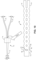
- the transition section of taper is replaced by a "waggled" waveguide transition section 180 as represented by the lower drawing of Fig. 10 .
- the waggled transition section 180 has an initial width of about 2w, then abruptly shifts to 2 waveguide segments 182, 184 each of width w separated by a gap 186 of g, forming what can be termed a gapped segment. After a very short distance it 'wags' back to a single waveguide, ungapped segment 188 of width 2w, forming what can be termed an ungapped segment.
- Connecting segments 190, 192 connect waveguide segments 182, 184 of the gapped segment with the single waveguide segment 172 and the ungapped segment 188, respectively.
- This alternation of double and single waveguide sections can repeat several times, in each subsequent cycle generally, the fraction of length having two separate waveguides can increases and the fraction of length having a single waveguide can decrease, although there can be adjacent wags in which the fraction of lengths can remain approximately the same for one or a few cycles.
- the total number of alternating segments shown as 10 wags (10 ungapped segments and 10 gapped segments), can more generally be at least 3 wags, in some embodiments from 4 to about 75 wags in a transition section, in further embodiments from 5 to 50 and in other embodiments from 6 to 25 wages in a transition section.
- a waveguide core generally extends over many hundreds of microns or longer without significant disruption in order to 'guide' a wave. Although it is common and conventional, and correspondingly used herein, to refer to shorter structures of waveguide core as 'waveguides', more precisely they are 'refractive elements', and that distinction should be considered to understand the behavior of the waggled waveguide transition. While not wanting to be limited by the summary simplifications, some observations are made regarding the operation of the devices described herein.
- the optical signal does not immediately split up and follow the waveguide cores in and out; instead the optical signal reacts to the refractive nature of the pattern.
- the optical signal in such a structure extends greater in width than the actual structure of the core elements.
- the desired waveguide transition should accomplish two things: (a) the central peak of the input mode should be smoothly split into two peaks approximately aligning to the output waveguides and separated by a dip; and (b) the wavefront should remain flat so it is neither converging nor diverging.
- the ideal splitter accomplishes both of these (as a theoretical device) and hence its extraordinary (theoretical) efficiency.
- the other approaches to reduce optical loss of a Y-branch splitter discussed above prior to the present invention tend not to directly address either of these, or at best only address (a).
- the other approaches e.g., Fig. 7
- the other approaches generally make (b) worse than doing nothing, and clearly it is desirable for improved optical splitting, as available with the embodiment of Fig. 10 .
- the structure of the waggled transition is further elaborated in Fig. 11 .
- a key principle is highlighted in that there is a waveguide 'profile-A' on the input waveguide 200 and a composite 'profile-B' at the interface of transition section 202 to output waveguides 204, 206 collectively forming the profile-B, where both profile-A and profile-B can be practically fabricated.
- the principle of the waggled transition is straightforward: the structure alternates between profile-A and profile-B several times with cycles nearer the input being a larger fraction of length in profile-A and cycles nearer the output having a greater fraction of the length in profile-B.
- the alternative profile segments have connecting sections C between them.
- each cycle (depicted as 'p') does not need to be constant throughout the transition, and the progression of profile lengths (depicted as n*dq), starting from an initial profile length q 0 , does not need to be uniform, but should be generally increasing, although not necessarily on every cycle.
- a suitable value for dq would be about 0.25 microns.
- suitable performance can be achieved with a wide range of variation in the waggles.
- constant 'p' and uniform 'dq' works quite well. Numerical examples for dimensions are provided later in this document where results are discussed.
- Figs. 10 and 11 depict slanted coupling segments between the profiles. This is not crucial to the basic efficiency of the transition, and other shapes to these connecting segments can be suitably efficient. There are however some other advantages to these slants that will be described shortly. In particular though, processing considerations that result in imperfections to the connecting segments that can be less pronounced with appropriate selection to the connecting segments.
- the total amount of core across profile-A e.g., an ungapped segment
- the core across profile-B e.g., a gapped segment.
- the desirable results can relax this condition such that according to the claimed invention, the core across profile-A can be within ⁇ 10% of the core structure across profile-B and in some embodiments within ⁇ 5% of the core structure across profile-B.
- the core width across the profile-A and profile-B segments can have minor variations across transition section from segments of the same type within the same ranges ⁇ 10%, ⁇ 5%.
- the profile-A segments start at the input side larger in extent in the propagation direction than the profile-B segments, but gradually the profile-A segments get smaller in extent in the propagation direction while the profile-B segments get larger.
- additional ranges of relative core amounts across the profiles and extents of the profiles in the propagation direction within the explicit ranges above are contemplated and are within the present disclosure.
- the core structures were referred to as refractive elements and that they induced a local delay along the optical wavefront. If that delay is over the right extent of area, then the tendency for the optical wavefront to curve inwards from the delay balances the tendency for it to curve outwards from propagation, and the wavefront remains nominally straight. If there is too much core crossing the path, the wavefront can be over-delayed and overall bow inward. If there is too little core crossing, the wavefront can bow outwards. Keeping the total cross-section of core across the central region of the wavefront approximately constant helps to keep the wavefront straight, providing access to higher efficiency and reduced noise ('sloshing') in the output waveguides.
- the total amount of core in the cross-section remains approximately constant, even as it wags from one profile to the other (one of the advantages of slants).
- the holes in the core at the center of the structure are mirrored in the upper and lower appendages to the core with half of the hole filled at the top and the other half of the hole filled at the bottom to keep the amount of core width approximately the same although split.
- the optical performance is not strongly dependent on the shape of the connecting segments, which can have a shorter extent in the propagation direction.
- Another advantage of the designs herein is a direct consequence of the above approximately constant-total cross-section through the transition zone.
- the total transverse extent of the core input-like profile-A is less than the total transverse extent of core output-like profile-B (the outer edges of the transition zone have to jut outwards to go from A to B) due to the gap in the profile-B segments. This shift happens since the width of profile-A is roughly 2*w and no gap, while the width of profile-B is roughly 2*w plus a gap.
- the gap at the profile-B segments can change from the input end to the output end, such as a gradual transition.
- a segment with three wags is shown.
- input section has a width 2w
- profile-B segments 222, 224, 226 have, respectively, gaps g 1 , g 2 , g 3 with g 1 ⁇ g 2 ⁇ g 3 .
- Profile-A segments 228, 230, 232, 234 are equivalent to corresponding profile-A segments of Figs. 10 and 11 as well as the input section.
- the connecting segments change accordingly to account for the changing gaps.
- the initial gap can be selected to be the smallest practical gap, and this gap can grow slowly by the end of the transition section.
- the gap can be constant for several waggles, and then change, etc.
- Fig. 13 depicts a portion of a waggled transition 250 with no slant between the profiles. In other words, there are approximately no connecting segments between the profile-A segments and the profile-B segments.
- the depicted portion of waggled transition 250 comprises profile-A segment 252, profile-B segment 254 and profile-A segment 256.
- Profile-B segment 254 has an approximately rectangular gap 258. Simulations predict that a transition region with no slants, i.e., no connecting segments, would couple approximately as efficiently as a connecting segment with the slants, however there are some secondary considerations that can make the slants preferable.
- the simulations are not particularly sensitive to the precise shape of the connecting segments, which generally had a longitudinal extent less than the profiled segments.
- the shaded areas in Fig. 13 depict 90° interior angles that the fabrication process tries to produce.
- the design rules do allow 90° interior angles at roughly minimum dimensions, but when they are there the fabrication process should be carefully controlled to produce them. In that case, such features may restrict the fabrication process in areas that might otherwise be adjusted to improve other types of features, meaning restricted processing flexibility.
- the vertical edges depicted in Fig. 13 can reflect small amounts of light back along the input direction.
- the connecting segments has an extent along the propagation direction of the waveguides generally no more than 25% of the smallest transverse extent of the profiled segments or 50% of the gap.
- transition section portion 270 comprises profile-A segment 272, connecting segment 274, profile-B segment 276, connecting segment 278 and profile-A segment 280.
- Profile-B segment includes a rectangular portion of gap region 282, with triangular portions of gap region 282 extending into connecting segment 274 and connecting segment 278.
- gap region 282 has a hexagonal shape. In addition to the previously-mentioned improvement in managing constant cross-section, this also addresses the other two issues raised regarding the vertical connections of Fig. 13 . It can be seen in Fig.
- Fig. 15 depicts a simulated performance of a Y-branch splitter with a transition section described with respect to Figs. 10 and 11 .
- the simulations herein were performed with 10 wags.
- a corresponding device layout is depicted in Fig. 16 for facilitated viewing, which is not at a constant longitudinal scale; the waggled transition shows fewer cycles and is elongated compared to the other structures to better emphasize its structure.
- the transition is designed to the example parameters described earlier: refractive-index contrast is 1.5%, output waveguides are 4 ⁇ wide each, and the gap between the output waveguides is 2 ⁇ .
- a desirable solution is achieved with 10.5 cycles (counting the last transition from profile-A to profile-B as a half a cycle that continues with the split waveguides) with a cycle length of 7 ⁇ for a total length of the transition section of about 75 ⁇ .
- the growth along the optical path of the profile-B sections and the shortening of the profile-A sections approximately compensate for each cycle so that the cycle length remains approximately constant, but other variations of the cycle length can be used.
- the waggled transition section replaces a transition section as shown in Fig. 4 , where the input would taper from 8 ⁇ wide up to 10 ⁇ wide. For these parameters, that taper section would normally be about 200 ⁇ long, so the devices described herein also can reduce the footprint of the transition.
- Fig. 15 Simulation results for this structure are depicted in Fig. 15 .
- Earlier parts of the input taper are not shown for the simulation, but the optical intensity does not change significantly in the earlier parts of the taper.
- the described waggling transition sits between about 500 and 580 ⁇ along Z. If this is compared to Fig. 3 , 6 and 9 , it can be recognized that this transition behaves much more like the ideal splitter, with the central peak in the input having a well-behaved splitting into two symmetrical peaks before coupling into the output waveguides. This behavior is further supported by the graph in Fig. 17 showing well-behaved and efficient coupling of about 98% of ideal into each output waveguide for the same structure.
- Figs. 18A-C assemble simulations and amplitude plots for the traditional embodiment of Fig. 4 (18A), exemplary improvement of Fig. 7 (18B), and exemplified waggled embodiment (18C) for more direct comparison.
- These Figs. are reproduced from earlier figures, 18A from Figs. 5 and 6 , 18B from Figs. 8 and 9 and 18C from Figs. 15 and 17 .
- the models used to generate Fig. 18B and Fig. 18C were each individually optimized for improved performance with respect to the specific general design. Note that one could combine both the connecting paths of Fig. 7 and a waggled transition, such as Fig. 10 , since they are applied to different parts of the splitter. However, since the waggled transition already provides a clean separation and coupling to the output modes, the added connecting paths would not provide any significant benefit and may actually cause some additional scattering and loss of their own.
- Figs. 19A-C provide another set of comparisons based on simulated propagation through the comparative structures.
- the plots in Figs. 19A-C show a cross section of the optical intensity at a variety of locations along the relevant area of the plane of the splitter.
- simulation of the ideal (effectively unrealizable) splitter of Fig. 1 shows a well behaved and clean conversion from the centrally-peaked to the dual-peaked optical intensity function with a smooth dip between. This behavior is an indication that a straight wavefront is being approximately maintained through the transition.
- Fig. 19B shows the optical intensity function for the embodiment of Fig. 4 . Referring to Fig.
- Fig. 20 shows optical cores of a planar optical structure for introducing these modes.
- the discussion of Y-splitter function has only considered the lowest order mode, in which the intensity is centrally peaked, or separated into two peaks but the intervening dip not touching zero until the output waveguides are sufficient separated.
- the lowest order optical mode is referred to as a zero order mode since it has no zero-crossing
- the next order mode is referred to as a first order mode since it has one zero-crossing.
- the first order mode naturally has two lateral peaks, and the dip between them passes abruptly through zero intensity so that one peak is 180° out of phase with the other (i.e.
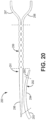
- a higher order splitter 290 comprises waggled Y-splitter 291 and curved coupled waveguide 292.
- Curved coupled waveguide 292 tapers to a termination point, which generally drives the coupling of optical intensity into the adjacent coupled waveguide of waggled Y-splitter 291.
- curved coupled waveguide 292 comprises an input waveguide section 293, a coupling waveguide section 294 identifiable by having significant coupling to Y-splitter 291, and terminating section 295, in which rough divisions are marked on the figure, although precise divisions of the sections is not significant for defining the structure or understanding its function.
- Waggled Y-splitter 291 comprises input waveguide section 296, first output waveguide section 297, second output waveguide section 298 and waggled transition section 299. Any of the various Y-splitter embodiments discussed above can be adapted for this device and are hereby incorporated into this discussion.
- Curved coupled waveguide 292 approaches input waveguide section 296 to form an adiabatic optical coupler. Curved coupled waveguide 292 below input waveguide section 296 in Fig. 20 couples light into the higher-order mode of the wider input waveguide section 296 of waggled Y-splitter 291.
- curved coupled waveguide 292 can be efficiently coupled, e.g., adiabatically coupled, into the first-order mode of waggled Y-splitter 291.
- the adiabatic coupling of a curved single mode waveguide with a multimode waveguide in close proximity is described in published U.S. patent application 2005/0254750 to Narevicius, entitled “Method and Apparatus for Optical Mode Division Multiplexing and Demultiplexing". This relationship allows the structure of Fig. 20 to operate as an optical mixer, useful as an output coupler of an optical switch, optical modulator, or polarization-state splitter, as discussed further below.
- An optical mixer can split a single optical signal from either input equally between the outputs, but if signal is present on both inputs, the optical interference between those two signals can direct the total optical power predominantly towards one or the other of the outputs.
- the ratio between the maximum optical power that can be directed to a single output and the minimum optical power that can be directed to that output is called the 'extinction ratio'.
- Applications employing an optical mixer generally prefer as high an extinction ratio as possible. This means being able to achieve very close to zero light in an output when the two input signals have equal intensity and proper phase. According to the basic principles of interference, approximating that zero signal requires nearly-equal efficiency for splitting both of the individual modes. For structures as depicted in Fig. 20 , it is desirable for the splitter to be able to split efficiently either mode (zero order mode or a first order mode).
- FIGs. 21A-C depict the effectiveness of splitting with respect to the first-order mode in a 2 x 2 splitter embodiment with three different embodiments for the Y-splitter component. Since the power in the first-order mode is near zero along the center of the waveguide axis, the splitting is not significantly adversely affected by encountering a finite gap. The optical wave is already naturally separated into two peaks, and hence couples well to the output waveguides.
- Fig. 20A shows that even with the Y-splitter embodiment of Fig. 4 , the simple, practical Y-Branch splits this higher-order mode efficiently.
- Fig. 21B the connecting paths of the Y-splitter embodiment of Fig.
- the splitting efficiency of the splitter be equal for each mode, not necessarily as high as possible.
- the splitting efficiency of the modes can be made approximately equal and still very high. For instance, by making the two waveguides in profile-B slightly wider than half the width of profile-A, one is designing away from the optimal efficiency for the zero-order mode, but towards the optimal efficiency of the first-order mode. Within a small range of design options, one can readily identify the crossover point where splitting of both modes is equally efficient.
- the zero order mode and the first order mode can have splitting efficiencies within 1 percent of each other, in further embodiments within 0.5 percent of each other and in additional embodiments within 0.25 percent of each other.
- additional ranges of efficiency differences within the explicit ranges above are contemplated and are within the present disclosure. No corresponding adjustments are known for the Y-splitter designs of Figs. 4 and 7 such that the efficiency of the higher-order mode would be expected to always be higher than for the low-order mode, unless you make them both very bad, which is not a reasonable alternative.
- input waveguide section 296 of Y-splitter 291 can include a zero order mode with a particular phase relationship with a zero order mode of curved coupled waveguide 292.
- the zero order mode of curved coupled waveguide 292 couples into a first order mode within Y-splitter 291, and the two optical signals can then interfere. If a zero order mode propagates from input waveguide section 296 and a first order mode couples into Y-splitter 291 from curved coupled waveguide 292, interference between the two modes concentrates the optical signal power towards one side or the other depending on the phase difference between the two inbound modes.
- the input signals into input waveguide section 296 and curved coupled waveguide 292 can have the same phase such that the interfering signals then constructively interfere over one portion of the first order signal and destructively interfere over the other portion of the first order signal to result in an asymmetric signal across the transverse direction of the waveguide.
- the asymmetric signal then is aligned to proceed into only one of the output waveguide sections 297, 298.
- the signals in the input waveguide section 296 and the curved coupled waveguide 292 are 180 degrees out of phase, the signals interfere with the constructive and destructive contributions reversed in space to form the opposite asymmetric signal, which is then aligned to enter the opposite output waveguide section 297, 298.
- Smaller degrees of phase misalignment can be used to adjust the amount of signal in each output waveguide based on the interference of the two signals combined in the input waveguide section 296. In this way, by adjusting the relative phase between two signals in the two output waveguides to provide a switching function which can be continuously adjusted between all of the signal in one output waveguide section or the other output waveguide section, e.g., variable optical attenuation and/or effective switching between one output or the other.
- the optical signals convey polarization dependent information
- the phases of the distinct polarization separately interfere in the combined signal with the device of Fig. 20 .
- the different polarization states can be directed into different output waveguide sections if the different polarizations have different phases relative to each other such that the opposite phases interfere differently for the opposite polarizations.
- the device of Fig. 20 can then be used as the final mixer of a polarization beam splitter.
- the switching functions whether or not based on polarization can be desirably accomplished with the device of Fig. 20 is the zero order modes and the first order modes are split by the waggled Y-splitter of Fig. 20 with approximately the same efficiency since then this leads to higher-extinction-ratio performance in the switching function.
- Fig. 22 depicts an asymmetric configuration based on the concepts presented herein that can be used with practical configurations to create splitters between 50% / 50% and about 80% / 20% based on the example parameters used herein and described above. With different parameters, a modified range of asymmetric splitting with this structure may be possible. With the broken symmetry, optical splitters have been difficult to realize with any of the known methods based on the Y-splitter structures. Asymmetric splitter designs based on the general Y-splitter designs tend to be very sensitive to wavelength changes and process variations, often too much so for practical applications. Since the waggled transition emulates the behavior of an ideal splitter of Fig. 1 , the wavelength dependence and process tolerance can be substantially improved with practical designs.
- asymmetric splitter 300 comprises input section 302, major output section 304, minor output section 306 and transition section 308.
- Major output section 304 has a greater width than minor output section 306.
- the width of the output waveguides are asymmetrical adjacent to the transition region, and the gap is correspondingly asymmetrically positioned.
- the ratios of the asymmetric widths of the output waveguides may be roughly selected based on the desired ratios of the output optical intensity, but simulations or empirical evaluation can adjust these selections to achieve the desired optical output.
- the gap occurs lower in the transition section as the width of the lower output waveguide decreases relative to the upper.
- the width of the major output waveguide is generally between about w and about 2w.
- the width of the minor output waveguide, and hence the position of the gap, cannot be reduced below the minimum width supported by the process design rules, for instance about 2-microns for the process of the examples herein.
- the entire output waveguide profile can be shifted relatively lower as described in embodiments below. Referring to Fig.
- input section 302 tapers from an initial width of w to a width of w 1 +w 2 +g, where w 1 is the width of major output section 304, w 2 is the width of minor output section 306, and g is the gap.
- w 1 /w 2 can be at least about 1.1, i.e., w 1 is 10% greater than w 2 .
- w 1 /w 2 can range from about 1.1 to 8, in further embodiments from about 1.2 to about 6 and in additional embodiments from about 1.3 to about 4.
- additional ranges of optical splitting and width ratios within the explicit ranges above are contemplated and are within the present disclosure.
- transition section 308 comprises 8 segments of profile-B 310 (one representative segment labeled in the figure) and 8 segments of profile-A 312 (one representative segment labeled in the figure), which have widths of w 1 +w 2 .
- Profile-B segments 310 have profiles with an upper waveguide of width w 1 and a lower waveguide portion of width w 2 separated by a gap g.
- Connecting segments 314 connect profile-A segments 312 with profile-B segments 310.
- the discussions above relevant to this asymmetric embodiment include, but are not limited to, the discussion above of the number of profile-A and profile-B segments in a transition section (e.g., 3-100), changes in the longitudinal extent along the optical path of the profile-A segments and profile-B segments from the input end to the output end of the transition section (e.g., q 0 + n ⁇ dq), the comparison of the transverse width of the core material at the profile-A segments and profile-B segments (e.g., approximately equal or ⁇ 25%), the nature of the connecting segments (e.g., presence or absence as well as shape and size), and other appropriate parameters.
- the number of profile-A and profile-B segments in a transition section e.g., 3-100
- changes in the longitudinal extent along the optical path of the profile-A segments and profile-B segments from the input end to the output end of the transition section e.g., q 0 + n ⁇ dq
- the output waveguides should be shifted away from the centerline of the input waveguide.
- the edges of the profile-A segments of the transition region are correspondingly shifted to maintain alignment with the output waveguides.
- this shifting results in a downward shift of the edges, with the upper bump getting smaller and the lower bump getting larger relative to the profile-B segments.
- the upper bump can vanish so that the upper edge of the profile-A segments and profile-B segments align ( Fig.
- a more frequently sought after type of asymmetric splitting is to split off a smaller fraction of the light, usually 10% or less, to use as a monitor signal while the large majority of the optical signal is routed forward through a single waveguide to the subsequent optical circuitry.
- the structure within this description of a small splitting device is generally referred to as an optical 'tap', the minor output waveguide being an optical tap waveguide.
- Embodiments of optical splitters related to applications of the waggled splitters to low-percentage optical taps are depicted in Figs. 23 and 24 .
- Intermediate shifted output waveguides between the embodiments of Fig. 22 and Fig. 23 are clear based on the description above with all of the configuration parameters continuously adjustable within processing capabilities.
- the upper edge of the output profile can align to the upper edge of the input waveguide, making the upper edge of the waggled transition approximately straight along its length as in optical tap 330 of Fig. 23 .
- the widths of the major output waveguide and the minor output waveguide can be adjusted similarly to the output waveguide widths of Fig. 22 .
- changing the amount of shift of the output waveguides as well as the ratio of the widths adjusts the optical splitting performance, and simulations and/or empirical adjustment can be used to achieve the desired degree of splitting.
- the bump up at profile-B segments for the lateral edge relative to a profile-A segment can range continuously from g/2 ( Fig. 22 ) to 0 ( Fig. 23 ) to negative values ( Fig. 24 ), as selected to provide a desired asymmetric split.
- Optical tap 330 comprises input waveguide section 332, output waveguide section 334, waveguide tap 336 and transition section 338.
- Transition section 338 comprises waggles with 8 profile-B segments 340 (one representative profile-B segments labeled) and 8 profile-A segments 342 (one representative profile-A section labeled) with connecting segments 344 connecting profile-A segments 342 and profile-B segments 340.
- Input waveguide section 332 generally tapers from an initial width of w to a width of w o + w t , where w o is the width of the primary output waveguide section 334 and w t is the width of waveguide tap 336.
- w 0 is between w and 2w.
- Profile-B segments generally have an upper waveguide portion with a width w o a lower waveguide portion with a width w t separated by a gap g.
- the width of the upper waveguide would taper back down from w o to w beyond the splitting region. Since the upper edge of the waveguide is approximately straight, the shift of the waggle in profile-B segments is only along the lower edge in this embodiment.
- the discussions above relevant to this asymmetric embodiment include, but are not limited to, the discussion above of the number of profile-A and profile-B segments in a transition section (e.g., 3-100), changes in the longitudinal extent along the optical path of the profile-A segments and profile-B segments from the input end to the output end of the transition section (e.g., q 0 +_n ⁇ dq), the comparison of the transverse width of the core material at the profile-A segments and profile-B segments (e.g., approximately equal or ⁇ 25%), the nature of the connecting segments (e.g., presence or absence as well as shape and size), and other appropriate parameters.
- the number of profile-A and profile-B segments in a transition section e.g., 3-100
- changes in the longitudinal extent along the optical path of the profile-A segments and profile-B segments from the input end to the output end of the transition section e.g., q 0 +_n ⁇ dq
- the output waveguides need to be offset even further from the centerline of the input waveguide.
- the upper edge of the output profile of the major output waveguide may be below the upper edge of the input profile.
- the upper edge may actually move inward where the transition wags to the wider profile as shown in the optical tap 360 of Fig. 24 .
- the degree of dipping can be selected to provide the desired tap output. This is the type of configuration that generally could be used to make taps of less than about 5% optical intensity.
- Waveguide taps with small tapping ratios e.g., below 10%
- a tap based on weak resonance coupling means that the tapping ratio generally varies significantly over the desired range of operating wavelengths, and there is a desire to be able to make a more stable small ratio tap.
- the types of taps depicted in Figs. 23 and 24 should be able to make such small-ratio taps with significantly improved wavelength stability.
- To Applicant's knowledge there is no corresponding idealized design based on the symmetric splitter of Fig. 1 . To Applicant's knowledge, no such tap designs exist based on the splitter concepts of Figs. 4 and 7 .
- optical tap 360 comprises input waveguide section 362, output waveguide section 364, waveguide tap 366 and transition section 368.
- Transition section 368 comprises waggles with 8 profile-B segments 370 (one representative profile-B segments labeled) and 8 profile-A segments 372 (one representative profile-A segment labeled) with connecting segments 374 connecting profile-A segments 372 and profile-B segments 370.
- Input waveguide section 362 generally tapers from an initial width of w to a width of about w o + w t , where w o is the width of the primary output waveguide 364 and w t is the width of waveguide tap 366.
- Profile-B segments generally have an upper waveguide section with a width w o , a lower waveguide section with a width w t separated by a gap, g. Since the lateral upper edge of the output waveguide is below the lateral upper edge of the end of input waveguide section 362, the waggles have a dip at the top of profile-B sections rather than a bump, and the lower extension of the waggles have lateral edges that correspondingly extend further down relative to the lower edge of the end of input waveguide section 362. Correspondingly the gaps at the profile-B sections are shifted lower in the embodiment of Fig. 24 relative to the embodiment of Fig. 23 . Again, for the embodiment of Fig.
- the reference to upper and lower is only for convenient reference to the drawing and is not intended to imply any actual orientation in space, and the device can be oriented in the flipped over configuration for taps to carry the signal in the other direction relative to the main optical waveguide.
- the general description of the alternative embodiment of the waggle structure above for the waggle transition in Fig. 10 can be correspondingly applied to the embodiment of Fig. 24 as appropriate for this embodiment and the above text is as if written here for corresponding alternative embodiments.
- the discussions above relevant to this asymmetric embodiment include, but are not limited to, the discussion above of the number of profile-A and profile-B segments in a transition section (e.g., 3-100), changes in the longitudinal extent along the optical path of the profile-A segments and profile-B segments from the input end to the output end of the transition section (e.g., q 0 + n ⁇ dq), the comparison of the transverse width of the core material at the profile-A segments and profile-B segments (e.g., approximately equal or ⁇ 25%), the nature of the connecting segments (e.g., presence or absence as well as shape and size), and other appropriate parameters.
- the number of profile-A and profile-B segments in a transition section e.g., 3-100
- changes in the longitudinal extent along the optical path of the profile-A segments and profile-B segments from the input end to the output end of the transition section e.g., q 0 + n ⁇ dq
- the output waveguide sections initially have widths adjacent the transition section selected to provide a desired optical intensity splitting. Following the splitting, the output waveguide sections can gradually taper to have a width w to support the signal for transmission longer distances.
- the taps can be directed to an optical detector or the like after a short distance that may make a taper for the tap output section superfluous.
- Fig. 25 shows application of the invention to a 1 ⁇ 3 splitter.
- a 1 ⁇ 3 splitter 400 comprises input waveguide section 402, first output waveguide section 404, second output waveguide section 406, third waveguide section 408 and transition section 410.
- Transition section 410 is depicted with 6 alternating segments with profile-A and profile-B. Connecting segments are shown between each profile-A and profile-B segment.
- one profile-A segment 414 and one profile-B segment 412 are labeled in Fig. 25 along with adjacent connecting segments 416, 418.
- Profile-B segment 412 has three waveguide segments (with widths w 1 , w 2 , and w 3 separated from each other by a gap, g).
- Profile-A segment has a continuous core with a width of approximately w 1 +w 2 +w 3 .
- Fig. 26 shows application to a 2x3 optical mixer 430.
- Optical mixer 430 comprises 2 input waveguide sections 432, 434, three output waveguide sections 436, 438, 440 and transition section 442.
- Transition section 442 comprises as shown in the figure 5 profile-A segments and 5 profile-B segments with corresponding connecting segments.
- Profile-A segment 446 has three waveguide segments with widths w 1 , w 2 , w 3 separated by gaps, g.
- the gaps in the transition sections of Figs. 25 and 26 are shown with hexagonal shapes similar to those of Fig. 10 . However, for these embodiments, the hexagonal gaps do not correspond with connecting segments having the core material with the same later width as the lateral width of core in the profile-A segments and the profile-B segments. According to simulations, the change in the lateral width of the core material in the connecting segments does not influence the performance significantly, and the hexagonal shaped gaps generally provide for convenient processing. Generally, other reasonable gap shapes can be used for the various embodiments.
- the embodiments in Figs. 25 and 26 can have different numbers of profile-A and profile-B segments as described above for the other embodiments. Also, the general description of the alternative embodiment of the waggle structure above for the waggle transition in Fig.
- the discussions above relevant to this asymmetric embodiment include, but are not limited to, the discussion above of the number of profile-A and profile-B segments in a transition section (e.g., 3-100), changes in the longitudinal extent along the optical path of the profile-A segments and profile-B segments from the input end to the output end of the transition section (e.g., q 0 + n ⁇ dq), the comparison of the transverse width of the core material at the profile-A segments and profile-B segments (e.g., approximately equal or ⁇ 25%), the nature of the connecting segments (e.g., presence or absence as well as shape and size), and other appropriate parameters.
- the number of profile-A and profile-B segments in a transition section e.g., 3-100
- changes in the longitudinal extent along the optical path of the profile-A segments and profile-B segments from the input end to the output end of the transition section e.g., q 0 + n ⁇ dq
- the materials for forming the planar devices described herein within a PLC can be deposited on a substrate using CVD, variations thereof, flame hydrolysis or other appropriate deposition approach.
- Suitable substrates include, for example, materials with appropriate tolerance of higher processing temperatures, such as silicon, ceramics, e.g., silica or alumina, or the like.
- suitable silicon dioxide precursors can be introduced, and a silica glass can be doped to provide a desired index of refraction and processing properties. Similar, deposition and doping can be performed for other optical materials.
- the patterning can be performed with photolithography or other suitable patterning technique.
- a silica glass doped with Ge, P and B based on plasma enhanced CVD (PECVD) for use as a top cladding layer for a PLC is described in U.S. patent 7,160,746 to Zhong et al. , entitled “GEBPSG Top Clad for a Planar Lightwave Circuit”.
- PECVD plasma enhanced CVD
- a core for the optical planar waveguides is described, for example, in U.S. patent 6,615,615 to Zhong et al. , entitled "GEPSG Core for a Planar Lightwave Circuit”.
- the devices described herein can be generally integrated with additional components within a planar lightwave circuit, although they alternatively can be incorporated as a single device within a planar lightwave circuit to connection to optical fibers and/or additional separate planar lightwave circuits using appropriate connectors.
Landscapes
- Physics & Mathematics (AREA)
- Engineering & Computer Science (AREA)
- Microelectronics & Electronic Packaging (AREA)
- General Physics & Mathematics (AREA)
- Optics & Photonics (AREA)
- Power Engineering (AREA)
- Optical Integrated Circuits (AREA)
Claims (9)
- Une jonction de guide d'ondes planaire comprenant- au moins une section de guide d'ondes d'entrée (172 ; 200 ; 228 ; 296 ; 302 ; 332 ; 362 ; 402),- au moins deux sections de guide d'ondes de sortie (176, 178 ; 204, 206 ; 297, 298 ; 304, 306 ; 334, 336 ; 364, 366 ; 404, 406, 408) et- une section de guide d'ondes de transition (180 ; 202 ; 220 ; 250 ; 270 ; 299 ; 308 ; 338 ; 368 ; 400) reliant optiquement l'au moins une section de guide d'ondes d'entrée (172 ; 200 ; 228 ; 296 ; 302 ; 332 ; 362 ; 402) et les au moins deux sections de guide d'ondes de sortie (176, 178 ; 204, 206 ; 297, 298 ; 304, 306 ; 334, 336 ; 364, 366 ; 404, 406, 408), la section de guide d'ondes de transition comprenant en alternance des segments à trou (182, 184 ; 222, 224, 226 ; 254 ; 310 ; 340 ; 370 ; 412) et des segments sans trou (188 ; 230, 232, 234 ; 252, 256 ; 272, 280 ; 312 ; 342 ; 372 ; 414) le long du chemin optique, les segments à trou (182, 184 ; 222, 224, 226 ; 254 ; 310 ; 340 ; 370 ; 412) ayant, transversalement au chemin optique, des segments d'âme de guide d'ondes correspondant aux au moins deux sections de guide d'ondes de sortie (176, 178 ; 204, 206 ; 297, 298 ; 304, 306 ; 334, 336 ; 364, 366 ; 404, 406, 408) séparés par des trous (186 ; 258 ; 282) dans l'âme optique, et les sections segments sans trou (188 ; 230, 232, 234 ; 252, 256 ; 272, 280 ; 312 ; 372 ; 414) ayant une âme transversale continue ayant une largeur totale dans les ± 10 % de la somme totale de largeur transversale de l'âme au niveau des segments à trou (182, 184 ; 222, 224, 226 ; 254 ; 310 ; 340 ; 370 ; 412),- dans laquelle la section de transition a au moins 3 segments à trou (182, 184 ; 222, 224, 226 ; 254 ; 310 ; 340 ; 370 ; 412) et au moins 3 segments sans trou (188 ; 230, 232, 234 ; 252, 256 ; 272, 280 ; 312 ; 342 ; 372 ; 414), et- dans laquelle la section d'entrée a un segment de largeur constante le long d'un chemin optique avant un segment conique et relié optiquement à celui-ci où l'âme s'élargit et, plus loin sur un chemin optique, est reliée à la section de transition et dans laquelle le trou (186 ; 258 ; 282) est d'environ 0,25 w à environ 0,9 w, où w est l'étendue transversale perpendiculaire au chemin optique de l'âme de guide d'ondes d'entrée le long du segment de largeur constante avant le segment conique relié à la section de transition.
- La jonction de guide d'ondes planaire de la revendication 1 dans laquelle l'au moins une section de guide d'ondes d'entrée (172 ; 200 ; 228 ; 296 ; 302 ; 332 ; 362 ; 402) est une section de guide d'ondes d'entrée (172 ; 200 ; 228 ; 296 ; 302 ; 332 ; 362 ; 402) et les au moins deux sections de guide d'ondes de sortie (176, 178 ; 204, 206 ; 297, 298 ; 304, 306 ; 334, 336 ; 364, 366 ; 404, 406, 408) sont deux sections de guide d'ondes de sortie (176, 178 ; 204, 206 ; 297, 298 ; 304, 306 ; 334, 336 ; 364, 366 ; 404, 406, 408), de telle sorte que la jonction de guide d'ondes planaire est un séparateur 1 x 2.
- La jonction de guide d'ondes planaire de la revendication 1 ou de la revendication 2 dans laquelle la section de transition a de 6 à 25 segments à trou (182, 184 ; 222, 224, 226 ; 254 ; 310 ; 340 ; 370 ; 412) et de 6 à 25 segments sans trou (188 ; 230, 232, 234 ; 252, 256 ; 272, 280 ; 312 ; 342 ; 372 ; 414).
- La jonction de guide d'ondes planaire de l'une quelconque des revendications 1 à 3 dans laquelle un segment de liaison (190, 192 ; 274, 278 ; 314 ; 344 ; 374 ; 416, 418) relie un segment à trou (182, 184 ; 222, 224, 226 ; 254 ; 310 ; 340 ; 370 ; 412) à un segment sans trou adjacent (188 ; 230, 232, 234 ; 252, 256 ; 272, 280 ; 312 ; 342 ; 372 ; 414).
- La jonction de guide d'ondes planaire de la revendication 4 dans laquelle le trou (186 ; 258 ; 282) s'étendant d'un côté à l'autre d'un segment à trou (182, 184 ; 222, 224, 226 ; 254 ; 310 ; 340 ; 370 ; 412) et de deux segments de liaison adjacents (190, 192 ; 274, 278 ; 314 ; 344 ; 374 ; 416, 418) forme approximativement un hexagone.
- La jonction de guide d'ondes planaire de l'une quelconque des revendications 1 à 5 dans laquelle les sections de guide d'ondes de sortie (176, 178 ; 204, 206 ; 297, 298 ; 304, 306 ; 334, 336 ; 364, 366 ; 404, 406, 408) sont asymétriques.
- La jonction de guide d'ondes planaire de la revendication 6 dans laquelle une section de guide d'ondes de sortie (176, 178 ; 204, 206 ; 297, 298 ; 304, 306 ; 334, 336 ; 364, 366 ; 404, 406, 408) a une largeur qui est un facteur d'environ 1,1 à environ 4 fois la largeur de la deuxième section de guide d'ondes de sortie (176, 178 ; 204, 206 ; 297, 298 ; 304, 306 ; 334, 336 ; 364, 366 ; 404, 406, 408).
- La jonction de guide d'ondes planaire de l'une quelconque des revendications 1 et 3 à 7 dans laquelle l'au moins une section de guide d'ondes d'entrée (172 ; 200 ; 228 ; 296 ; 302 ; 332 ; 362 ; 402) est une section de guide d'ondes d'entrée (172 ; 200 ; 228 ; 296 ; 302 ; 332 ; 362 ; 402) et les au moins deux sections de guide d'ondes de sortie (176, 178 ; 204, 206 ; 297, 298 ; 304, 306 ; 334, 336 ; 364, 366 ; 404, 406, 408) sont trois sections de guide d'ondes de sortie (176, 178 ; 204, 206 ; 297, 298 ; 304, 306 ; 334, 336 ; 364, 366 ; 404, 406, 408), de telle sorte que la jonction de guide d'ondes planaire est un séparateur 1 x 3.
- La jonction de guide d'ondes planaire de l'une quelconque des revendications 1 et 3 à 7 dans laquelle l'au moins une section de guide d'ondes d'entrée (172 ; 200 ; 228 ; 296 ; 302 ; 332 ; 362 ; 402 ; 432, 434) consiste en deux sections de guide d'ondes d'entrée (172 ; 200 ; 228 ; 296 ; 302 ; 332 ; 362 ; 402 ; 432, 434) et les au moins deux sections de guide d'ondes de sortie (176, 178 ; 204, 206 ; 297, 298 ; 304, 306 ; 334, 336 ; 364, 366 ; 404, 406, 408 ; 436, 438, 440) consistent en trois sections de guide d'ondes de sortie (176, 178 ; 204, 206 ; 297, 298 ; 304, 306 ; 334, 336 ; 364, 366 ; 404, 406, 408, 436, 438, 440), de telle sorte que la jonction de guide d'ondes planaire est un combineur 2 x 3.
Applications Claiming Priority (2)
| Application Number | Priority Date | Filing Date | Title |
|---|---|---|---|
| US15/490,420 US10330863B2 (en) | 2017-04-18 | 2017-04-18 | Planar lightwave circuit optical splitter / mixer |
| PCT/US2018/027754 WO2018194966A1 (fr) | 2017-04-18 | 2018-04-16 | Diviseur/mélangeur optique à circuit planaire d'ondes lumineuses |
Publications (3)
| Publication Number | Publication Date |
|---|---|
| EP3612877A1 EP3612877A1 (fr) | 2020-02-26 |
| EP3612877A4 EP3612877A4 (fr) | 2021-01-06 |
| EP3612877B1 true EP3612877B1 (fr) | 2023-07-12 |
Family
ID=63789956
Family Applications (1)
| Application Number | Title | Priority Date | Filing Date |
|---|---|---|---|
| EP18787064.7A Active EP3612877B1 (fr) | 2017-04-18 | 2018-04-16 | Jonction de guide d'ondes planaire |
Country Status (6)
| Country | Link |
|---|---|
| US (2) | US10330863B2 (fr) |
| EP (1) | EP3612877B1 (fr) |
| JP (1) | JP7198769B2 (fr) |
| CN (2) | CN110720065B (fr) |
| DK (1) | DK3612877T3 (fr) |
| WO (1) | WO2018194966A1 (fr) |
Families Citing this family (9)
| Publication number | Priority date | Publication date | Assignee | Title |
|---|---|---|---|---|
| US10416525B2 (en) | 2017-01-18 | 2019-09-17 | Neophotonics Corporation | Method and apparatus for phase-matched optical and RF wave propagations for semiconductor-based MZM modulators |
| EP3824571A4 (fr) * | 2018-07-17 | 2022-04-13 | CommScope Technologies LLC | Système de communication optique à fibres utilisant un diviseur de guide d'ondes optique asymétrique |
| WO2020086744A1 (fr) * | 2018-10-23 | 2020-04-30 | The Regents Of The University Of California | Multiplexeur en longueur d'onde comprenant des coupleurs optiques en cascade |
| CN109597162B (zh) * | 2018-12-27 | 2021-04-09 | 华为技术有限公司 | 平面光波导、plc芯片、光束整形结构及wss |
| CN112558223B (zh) * | 2021-01-06 | 2021-12-14 | 中国科学院上海微系统与信息技术研究所 | 混合模式转换器及其制备方法 |
| US11500198B2 (en) * | 2021-01-12 | 2022-11-15 | Globalfoundries U.S. Inc. | Waveguide bus with balanced optical waveguides and method, system, and software tool for automatic generation of a layout for the waveguide bus |
| EP4652486A1 (fr) * | 2023-01-18 | 2025-11-26 | Psiquantum, Corp. | Détecteur de photons compensé |
| US12541058B2 (en) | 2023-09-08 | 2026-02-03 | Taiwan Semiconductor Manufacturing Company Limited | Nested waveguide fan-out structure and methods for forming the same |
| US20250284057A1 (en) * | 2024-03-08 | 2025-09-11 | Honeywell International Inc. | Adaptive modal phase matching in waveguides for increased nonlinear conversion efficiency |
Citations (1)
| Publication number | Priority date | Publication date | Assignee | Title |
|---|---|---|---|---|
| CN106125198A (zh) * | 2014-02-21 | 2016-11-16 | 杭州天野通信设备有限公司 | 用于对全通信波段进行分光优化的光分路结构及制备方法 |
Family Cites Families (42)
| Publication number | Priority date | Publication date | Assignee | Title |
|---|---|---|---|---|
| JPH02226204A (ja) * | 1989-02-28 | 1990-09-07 | Tsukasa Nagao | 光学磁性体薄膜を用いた光回路 |
| EP0598966B1 (fr) | 1992-11-24 | 1999-02-10 | International Business Machines Corporation | Isolateur optique pour guide d'onde |
| DE69417986T2 (de) | 1993-11-01 | 1999-09-30 | Sumitomo Electric Industries, Ltd. | Optisches Abzweigelement |
| US5623568A (en) * | 1995-09-15 | 1997-04-22 | Lucent Technologies Inc. | Compact and fabrication tolerant high speed digital optical Y-switches |
| US5757995A (en) | 1995-12-27 | 1998-05-26 | Nhk Spring Co., Ltd. | Optical coupler |
| US5745618A (en) | 1997-02-04 | 1998-04-28 | Lucent Technologies, Inc. | Optical device having low insertion loss |
| US6003222A (en) | 1997-07-10 | 1999-12-21 | Lucent Technologies Inc. | Manufacture of tapered waveguides |
| US6058233A (en) | 1998-06-30 | 2000-05-02 | Lucent Technologies Inc. | Waveguide array with improved efficiency for wavelength routers and star couplers in integrated optics |
| KR20000039804A (ko) | 1998-12-16 | 2000-07-05 | 이계철 | 비대칭 y분기 광도파로를 이용한 디지털 광변조기 |
| JP2001124945A (ja) | 1999-10-28 | 2001-05-11 | Oki Electric Ind Co Ltd | Y分岐導波路 |
| JP2001255427A (ja) * | 2000-03-10 | 2001-09-21 | Oki Electric Ind Co Ltd | 光導波路及びその製造方法 |
| US6697552B2 (en) | 2001-02-23 | 2004-02-24 | Lightwave Microsystems Corporation | Dendritic taper for an integrated optical wavelength router |
| US6853769B2 (en) * | 2001-03-16 | 2005-02-08 | Lightwave Microsystems Corporation | Arrayed waveguide grating with waveguides of unequal widths |
| JP3726062B2 (ja) * | 2001-04-25 | 2005-12-14 | 日本発条株式会社 | 光合分波器 |
| US6615615B2 (en) | 2001-06-29 | 2003-09-09 | Lightwave Microsystems Corporation | GePSG core for a planar lightwave circuit |
| US7072473B2 (en) * | 2001-07-12 | 2006-07-04 | Pitney Bowes Inc. | Method and system for secure delivery and retrieval of documents utilizing a facsimile machine |
| US7160746B2 (en) | 2001-07-27 | 2007-01-09 | Lightwave Microsystems Corporation | GeBPSG top clad for a planar lightwave circuit |
| KR100464986B1 (ko) * | 2001-09-27 | 2005-01-05 | 한국엔지니어링플라스틱 주식회사 | 염소 및 염소화합물에 안정한 폴리아세탈 수지 조성물 및이의 제품 |
| US7006729B2 (en) * | 2001-12-31 | 2006-02-28 | Wavesplitter Technologies, Inc. | Optical components having reduced insertion loss |
| CA2368945A1 (fr) | 2002-01-21 | 2003-07-21 | Guomin Yu | Dispositif de guide d'ondes optiques a affaiblissement d'insertion peu eleve |
| US6873766B2 (en) | 2002-04-12 | 2005-03-29 | Corrado P. Dragone | Efficient waveguide arrays with nearly perfect element patterns |
| US7609918B2 (en) | 2002-05-28 | 2009-10-27 | Optun (Bvi) Ltd. | Method and apparatus for optical mode division multiplexing and demultiplexing |
| US7343071B2 (en) * | 2002-06-04 | 2008-03-11 | Ignis Technologies As | Optical component and a method of fabricating an optical component |
| US6970625B2 (en) * | 2002-07-12 | 2005-11-29 | Intel Corporation | Optimized Y-branch design |
| US6934446B2 (en) | 2003-03-27 | 2005-08-23 | Lucent Technologies Inc. | Optical waveguiding apparatus having reduced crossover losses |
| US6892404B2 (en) | 2003-04-09 | 2005-05-17 | Keith E. Harbin | Top bed sheet with fitted foot end |
| EP1656573A1 (fr) * | 2003-08-19 | 2006-05-17 | Ignis Technologies AS | Convertisseur de taille de point a optique integre et procede de fabrication |
| JP2005266381A (ja) * | 2004-03-19 | 2005-09-29 | Nec Corp | 導波路型光スプリッタ及びこれを備えた導波路型光モジュール |
| JP2006023623A (ja) * | 2004-07-09 | 2006-01-26 | Furukawa Electric Co Ltd:The | 光導波路回路 |
| JP2006039080A (ja) * | 2004-07-26 | 2006-02-09 | Nippon Sheet Glass Co Ltd | 分岐光導波路 |
| JP4361030B2 (ja) * | 2005-02-25 | 2009-11-11 | 日本電信電話株式会社 | モードスプリッタおよび光回路 |
| US8355608B2 (en) | 2010-04-12 | 2013-01-15 | Lockheed Martin Corporation | Method and apparatus for in-line fiber-cladding-light dissipation |
| JP2013122493A (ja) * | 2011-12-09 | 2013-06-20 | Furukawa Electric Co Ltd:The | 光分岐素子および光分岐回路 |
| US9335469B2 (en) * | 2012-01-31 | 2016-05-10 | Ignis Photonyx A/S | Planar optical branching circuit |
| CN102841407B (zh) * | 2012-09-20 | 2014-06-04 | 电子科技大学 | 一种波导型偏振光分束器 |
| US20150104130A1 (en) * | 2013-10-14 | 2015-04-16 | Cisco Technology, Inc. | Optical power splitter |
| CN203825227U (zh) * | 2014-02-21 | 2014-09-10 | 杭州天野通信设备有限公司 | 用于对全通信波段进行分光优化的光分路结构 |
| US10422957B2 (en) * | 2014-04-07 | 2019-09-24 | Luxtera, Inc. | Method and system for a low-loss optical Y-junction power splitter |
| CN104049301B (zh) * | 2014-06-27 | 2016-05-04 | 中南民族大学 | 超小非对称结构的孔型偏振分束器 |
| WO2016071345A1 (fr) | 2014-11-03 | 2016-05-12 | Consorzio Nazionale Interuniversitario Per Le Telecomunicazioni | Rotateur de polarisation et répartiteur photoniques intégrés et procédé associé |
| US9557486B2 (en) * | 2015-06-29 | 2017-01-31 | Elenion Technologies, Llc | Optimized 2×2 3dB multi-mode interference coupler |
| CN105116491B (zh) * | 2015-09-22 | 2018-04-24 | 东南大学 | 一种硅基槽波导集成型光功分器 |
-
2017
- 2017-04-18 US US15/490,420 patent/US10330863B2/en active Active
-
2018
- 2018-04-16 CN CN201880037966.9A patent/CN110720065B/zh active Active
- 2018-04-16 JP JP2019556697A patent/JP7198769B2/ja active Active
- 2018-04-16 CN CN202210527567.9A patent/CN115016062B/zh active Active
- 2018-04-16 WO PCT/US2018/027754 patent/WO2018194966A1/fr not_active Ceased
- 2018-04-16 DK DK18787064.7T patent/DK3612877T3/da active
- 2018-04-16 EP EP18787064.7A patent/EP3612877B1/fr active Active
-
2019
- 2019-05-09 US US16/407,779 patent/US11061187B2/en active Active
Patent Citations (1)
| Publication number | Priority date | Publication date | Assignee | Title |
|---|---|---|---|---|
| CN106125198A (zh) * | 2014-02-21 | 2016-11-16 | 杭州天野通信设备有限公司 | 用于对全通信波段进行分光优化的光分路结构及制备方法 |
Also Published As
| Publication number | Publication date |
|---|---|
| CN115016062A (zh) | 2022-09-06 |
| US11061187B2 (en) | 2021-07-13 |
| CN110720065B (zh) | 2022-05-31 |
| WO2018194966A1 (fr) | 2018-10-25 |
| CN110720065A (zh) | 2020-01-21 |
| US10330863B2 (en) | 2019-06-25 |
| WO2018194966A9 (fr) | 2019-10-24 |
| US20180299617A1 (en) | 2018-10-18 |
| JP7198769B2 (ja) | 2023-01-04 |
| EP3612877A4 (fr) | 2021-01-06 |
| EP3612877A1 (fr) | 2020-02-26 |
| DK3612877T3 (da) | 2023-10-16 |
| JP2020517990A (ja) | 2020-06-18 |
| CN115016062B (zh) | 2024-07-19 |
| US20190278023A1 (en) | 2019-09-12 |
Similar Documents
| Publication | Publication Date | Title |
|---|---|---|
| EP3612877B1 (fr) | Jonction de guide d'ondes planaire | |
| US8218932B2 (en) | Polarization independent optical device | |
| CN102099718B (zh) | 光波长合分波回路 | |
| US10393961B2 (en) | Mode matched Y-junction | |
| Memon et al. | Recent advances in mode converters for a mode division multiplex transmission system | |
| CN109564326A (zh) | 具有绝热弯曲部的单模波导 | |
| US8208772B2 (en) | Polarization independent directional coupler and related optical devices | |
| JPWO2008078561A1 (ja) | 導波路接続構造 | |
| JP6798313B2 (ja) | リブ型光導波路およびそれを用いた光合分波器 | |
| US8380023B2 (en) | Waveguide-type optical circuit | |
| JP5169536B2 (ja) | 光合分波素子 | |
| KR100417001B1 (ko) | 보조 광도파로를 구비한 광세기 분할기 | |
| JP4636439B2 (ja) | 方向性光結合器の2つの直線光導波路のコア幅及びコア間の距離の計算方法 | |
| CN117434652A (zh) | 一种低串扰低温漂的粗波分复用器 | |
| WO2010010878A1 (fr) | Structure de connexion de guide d'ondes | |
| CN104090331B (zh) | 一种高效紧凑矩形环谐振腔波导型光滤波器 | |
| JP2003248127A (ja) | 光パワー分割器 | |
| JP5091072B2 (ja) | Y分岐光導波路およびその設計方法 | |
| GB2395796A (en) | Optical waveguide branching component with MMI couplers | |
| JP5019649B2 (ja) | 導波路型光回路 | |
| JP2005274844A (ja) | 光制御素子 | |
| JP6175468B2 (ja) | 光導波路素子 | |
| JP2010164858A (ja) | 導波路型光回路 |
Legal Events
| Date | Code | Title | Description |
|---|---|---|---|
| STAA | Information on the status of an ep patent application or granted ep patent |
Free format text: STATUS: THE INTERNATIONAL PUBLICATION HAS BEEN MADE |
|
| PUAI | Public reference made under article 153(3) epc to a published international application that has entered the european phase |
Free format text: ORIGINAL CODE: 0009012 |
|
| STAA | Information on the status of an ep patent application or granted ep patent |
Free format text: STATUS: REQUEST FOR EXAMINATION WAS MADE |
|
| 17P | Request for examination filed |
Effective date: 20191118 |
|
| AK | Designated contracting states |
Kind code of ref document: A1 Designated state(s): AL AT BE BG CH CY CZ DE DK EE ES FI FR GB GR HR HU IE IS IT LI LT LU LV MC MK MT NL NO PL PT RO RS SE SI SK SM TR |
|
| AX | Request for extension of the european patent |
Extension state: BA ME |
|
| DAV | Request for validation of the european patent (deleted) | ||
| DAX | Request for extension of the european patent (deleted) | ||
| A4 | Supplementary search report drawn up and despatched |
Effective date: 20201207 |
|
| RIC1 | Information provided on ipc code assigned before grant |
Ipc: G02B 6/12 20060101ALI20201201BHEP Ipc: G02B 6/125 20060101AFI20201201BHEP |
|
| RAP3 | Party data changed (applicant data changed or rights of an application transferred) |
Owner name: NEOPHOTONICS CORPORATION |
|
| STAA | Information on the status of an ep patent application or granted ep patent |
Free format text: STATUS: EXAMINATION IS IN PROGRESS |
|
| 17Q | First examination report despatched |
Effective date: 20220103 |
|
| GRAP | Despatch of communication of intention to grant a patent |
Free format text: ORIGINAL CODE: EPIDOSNIGR1 |
|
| STAA | Information on the status of an ep patent application or granted ep patent |
Free format text: STATUS: GRANT OF PATENT IS INTENDED |
|
| RIC1 | Information provided on ipc code assigned before grant |
Ipc: G02B 6/126 20060101ALN20220819BHEP Ipc: G02B 6/12 20060101ALN20220819BHEP Ipc: G02B 6/125 20060101AFI20220819BHEP |
|
| INTG | Intention to grant announced |
Effective date: 20220909 |
|
| GRAJ | Information related to disapproval of communication of intention to grant by the applicant or resumption of examination proceedings by the epo deleted |
Free format text: ORIGINAL CODE: EPIDOSDIGR1 |
|
| STAA | Information on the status of an ep patent application or granted ep patent |
Free format text: STATUS: EXAMINATION IS IN PROGRESS |
|
| GRAP | Despatch of communication of intention to grant a patent |
Free format text: ORIGINAL CODE: EPIDOSNIGR1 |
|
| STAA | Information on the status of an ep patent application or granted ep patent |
Free format text: STATUS: GRANT OF PATENT IS INTENDED |
|
| INTC | Intention to grant announced (deleted) | ||
| RIC1 | Information provided on ipc code assigned before grant |
Ipc: G02B 6/126 20060101ALN20230125BHEP Ipc: G02B 6/12 20060101ALN20230125BHEP Ipc: G02B 6/125 20060101AFI20230125BHEP |
|
| INTG | Intention to grant announced |
Effective date: 20230206 |
|
| GRAS | Grant fee paid |
Free format text: ORIGINAL CODE: EPIDOSNIGR3 |
|
| GRAA | (expected) grant |
Free format text: ORIGINAL CODE: 0009210 |
|
| STAA | Information on the status of an ep patent application or granted ep patent |
Free format text: STATUS: THE PATENT HAS BEEN GRANTED |
|
| AK | Designated contracting states |
Kind code of ref document: B1 Designated state(s): AL AT BE BG CH CY CZ DE DK EE ES FI FR GB GR HR HU IE IS IT LI LT LU LV MC MK MT NL NO PL PT RO RS SE SI SK SM TR |
|
| REG | Reference to a national code |
Ref country code: CH Ref legal event code: EP |
|
| REG | Reference to a national code |
Ref country code: DE Ref legal event code: R096 Ref document number: 602018053269 Country of ref document: DE |
|
| REG | Reference to a national code |
Ref country code: IE Ref legal event code: FG4D |
|
| REG | Reference to a national code |
Ref country code: DK Ref legal event code: T3 Effective date: 20231010 |
|
| REG | Reference to a national code |
Ref country code: LT Ref legal event code: MG9D |
|
| REG | Reference to a national code |
Ref country code: NL Ref legal event code: MP Effective date: 20230712 |
|
| RAP4 | Party data changed (patent owner data changed or rights of a patent transferred) |
Owner name: NEOPHOTONICS CORPORATION |
|
| REG | Reference to a national code |
Ref country code: AT Ref legal event code: MK05 Ref document number: 1587746 Country of ref document: AT Kind code of ref document: T Effective date: 20230712 |
|
| PG25 | Lapsed in a contracting state [announced via postgrant information from national office to epo] |
Ref country code: NL Free format text: LAPSE BECAUSE OF FAILURE TO SUBMIT A TRANSLATION OF THE DESCRIPTION OR TO PAY THE FEE WITHIN THE PRESCRIBED TIME-LIMIT Effective date: 20230712 |
|
| PG25 | Lapsed in a contracting state [announced via postgrant information from national office to epo] |
Ref country code: GR Free format text: LAPSE BECAUSE OF FAILURE TO SUBMIT A TRANSLATION OF THE DESCRIPTION OR TO PAY THE FEE WITHIN THE PRESCRIBED TIME-LIMIT Effective date: 20231013 |
|
| PG25 | Lapsed in a contracting state [announced via postgrant information from national office to epo] |
Ref country code: ES Free format text: LAPSE BECAUSE OF FAILURE TO SUBMIT A TRANSLATION OF THE DESCRIPTION OR TO PAY THE FEE WITHIN THE PRESCRIBED TIME-LIMIT Effective date: 20230712 |
|
| PG25 | Lapsed in a contracting state [announced via postgrant information from national office to epo] |
Ref country code: IS Free format text: LAPSE BECAUSE OF FAILURE TO SUBMIT A TRANSLATION OF THE DESCRIPTION OR TO PAY THE FEE WITHIN THE PRESCRIBED TIME-LIMIT Effective date: 20231112 |
|
| PG25 | Lapsed in a contracting state [announced via postgrant information from national office to epo] |
Ref country code: SE Free format text: LAPSE BECAUSE OF FAILURE TO SUBMIT A TRANSLATION OF THE DESCRIPTION OR TO PAY THE FEE WITHIN THE PRESCRIBED TIME-LIMIT Effective date: 20230712 Ref country code: RS Free format text: LAPSE BECAUSE OF FAILURE TO SUBMIT A TRANSLATION OF THE DESCRIPTION OR TO PAY THE FEE WITHIN THE PRESCRIBED TIME-LIMIT Effective date: 20230712 Ref country code: PT Free format text: LAPSE BECAUSE OF FAILURE TO SUBMIT A TRANSLATION OF THE DESCRIPTION OR TO PAY THE FEE WITHIN THE PRESCRIBED TIME-LIMIT Effective date: 20231113 Ref country code: NO Free format text: LAPSE BECAUSE OF FAILURE TO SUBMIT A TRANSLATION OF THE DESCRIPTION OR TO PAY THE FEE WITHIN THE PRESCRIBED TIME-LIMIT Effective date: 20231012 Ref country code: LV Free format text: LAPSE BECAUSE OF FAILURE TO SUBMIT A TRANSLATION OF THE DESCRIPTION OR TO PAY THE FEE WITHIN THE PRESCRIBED TIME-LIMIT Effective date: 20230712 Ref country code: LT Free format text: LAPSE BECAUSE OF FAILURE TO SUBMIT A TRANSLATION OF THE DESCRIPTION OR TO PAY THE FEE WITHIN THE PRESCRIBED TIME-LIMIT Effective date: 20230712 Ref country code: IS Free format text: LAPSE BECAUSE OF FAILURE TO SUBMIT A TRANSLATION OF THE DESCRIPTION OR TO PAY THE FEE WITHIN THE PRESCRIBED TIME-LIMIT Effective date: 20231112 Ref country code: HR Free format text: LAPSE BECAUSE OF FAILURE TO SUBMIT A TRANSLATION OF THE DESCRIPTION OR TO PAY THE FEE WITHIN THE PRESCRIBED TIME-LIMIT Effective date: 20230712 Ref country code: GR Free format text: LAPSE BECAUSE OF FAILURE TO SUBMIT A TRANSLATION OF THE DESCRIPTION OR TO PAY THE FEE WITHIN THE PRESCRIBED TIME-LIMIT Effective date: 20231013 Ref country code: FI Free format text: LAPSE BECAUSE OF FAILURE TO SUBMIT A TRANSLATION OF THE DESCRIPTION OR TO PAY THE FEE WITHIN THE PRESCRIBED TIME-LIMIT Effective date: 20230712 Ref country code: ES Free format text: LAPSE BECAUSE OF FAILURE TO SUBMIT A TRANSLATION OF THE DESCRIPTION OR TO PAY THE FEE WITHIN THE PRESCRIBED TIME-LIMIT Effective date: 20230712 Ref country code: AT Free format text: LAPSE BECAUSE OF FAILURE TO SUBMIT A TRANSLATION OF THE DESCRIPTION OR TO PAY THE FEE WITHIN THE PRESCRIBED TIME-LIMIT Effective date: 20230712 |
|
| PG25 | Lapsed in a contracting state [announced via postgrant information from national office to epo] |
Ref country code: PL Free format text: LAPSE BECAUSE OF FAILURE TO SUBMIT A TRANSLATION OF THE DESCRIPTION OR TO PAY THE FEE WITHIN THE PRESCRIBED TIME-LIMIT Effective date: 20230712 |
|
| REG | Reference to a national code |
Ref country code: DE Ref legal event code: R097 Ref document number: 602018053269 Country of ref document: DE |
|
| PG25 | Lapsed in a contracting state [announced via postgrant information from national office to epo] |
Ref country code: SM Free format text: LAPSE BECAUSE OF FAILURE TO SUBMIT A TRANSLATION OF THE DESCRIPTION OR TO PAY THE FEE WITHIN THE PRESCRIBED TIME-LIMIT Effective date: 20230712 Ref country code: RO Free format text: LAPSE BECAUSE OF FAILURE TO SUBMIT A TRANSLATION OF THE DESCRIPTION OR TO PAY THE FEE WITHIN THE PRESCRIBED TIME-LIMIT Effective date: 20230712 Ref country code: EE Free format text: LAPSE BECAUSE OF FAILURE TO SUBMIT A TRANSLATION OF THE DESCRIPTION OR TO PAY THE FEE WITHIN THE PRESCRIBED TIME-LIMIT Effective date: 20230712 Ref country code: CZ Free format text: LAPSE BECAUSE OF FAILURE TO SUBMIT A TRANSLATION OF THE DESCRIPTION OR TO PAY THE FEE WITHIN THE PRESCRIBED TIME-LIMIT Effective date: 20230712 Ref country code: SK Free format text: LAPSE BECAUSE OF FAILURE TO SUBMIT A TRANSLATION OF THE DESCRIPTION OR TO PAY THE FEE WITHIN THE PRESCRIBED TIME-LIMIT Effective date: 20230712 |
|
| PLBE | No opposition filed within time limit |
Free format text: ORIGINAL CODE: 0009261 |
|
| STAA | Information on the status of an ep patent application or granted ep patent |
Free format text: STATUS: NO OPPOSITION FILED WITHIN TIME LIMIT |
|
| PG25 | Lapsed in a contracting state [announced via postgrant information from national office to epo] |
Ref country code: IT Free format text: LAPSE BECAUSE OF FAILURE TO SUBMIT A TRANSLATION OF THE DESCRIPTION OR TO PAY THE FEE WITHIN THE PRESCRIBED TIME-LIMIT Effective date: 20230712 |
|
| 26N | No opposition filed |
Effective date: 20240415 |
|
| PGFP | Annual fee paid to national office [announced via postgrant information from national office to epo] |
Ref country code: DK Payment date: 20240425 Year of fee payment: 7 |
|
| PG25 | Lapsed in a contracting state [announced via postgrant information from national office to epo] |
Ref country code: SI Free format text: LAPSE BECAUSE OF FAILURE TO SUBMIT A TRANSLATION OF THE DESCRIPTION OR TO PAY THE FEE WITHIN THE PRESCRIBED TIME-LIMIT Effective date: 20230712 |
|
| PG25 | Lapsed in a contracting state [announced via postgrant information from national office to epo] |
Ref country code: BG Free format text: LAPSE BECAUSE OF FAILURE TO SUBMIT A TRANSLATION OF THE DESCRIPTION OR TO PAY THE FEE WITHIN THE PRESCRIBED TIME-LIMIT Effective date: 20230712 |
|
| PG25 | Lapsed in a contracting state [announced via postgrant information from national office to epo] |
Ref country code: MC Free format text: LAPSE BECAUSE OF FAILURE TO SUBMIT A TRANSLATION OF THE DESCRIPTION OR TO PAY THE FEE WITHIN THE PRESCRIBED TIME-LIMIT Effective date: 20230712 |
|
| PG25 | Lapsed in a contracting state [announced via postgrant information from national office to epo] |
Ref country code: MC Free format text: LAPSE BECAUSE OF FAILURE TO SUBMIT A TRANSLATION OF THE DESCRIPTION OR TO PAY THE FEE WITHIN THE PRESCRIBED TIME-LIMIT Effective date: 20230712 Ref country code: BG Free format text: LAPSE BECAUSE OF FAILURE TO SUBMIT A TRANSLATION OF THE DESCRIPTION OR TO PAY THE FEE WITHIN THE PRESCRIBED TIME-LIMIT Effective date: 20230712 |
|
| REG | Reference to a national code |
Ref country code: CH Ref legal event code: PL |
|
| PG25 | Lapsed in a contracting state [announced via postgrant information from national office to epo] |
Ref country code: LU Free format text: LAPSE BECAUSE OF NON-PAYMENT OF DUE FEES Effective date: 20240416 |
|
| GBPC | Gb: european patent ceased through non-payment of renewal fee |
Effective date: 20240416 |
|
| REG | Reference to a national code |
Ref country code: BE Ref legal event code: MM Effective date: 20240430 |
|
| PG25 | Lapsed in a contracting state [announced via postgrant information from national office to epo] |
Ref country code: LU Free format text: LAPSE BECAUSE OF NON-PAYMENT OF DUE FEES Effective date: 20240416 |
|
| PG25 | Lapsed in a contracting state [announced via postgrant information from national office to epo] |
Ref country code: BE Free format text: LAPSE BECAUSE OF NON-PAYMENT OF DUE FEES Effective date: 20240430 |
|
| PG25 | Lapsed in a contracting state [announced via postgrant information from national office to epo] |
Ref country code: GB Free format text: LAPSE BECAUSE OF NON-PAYMENT OF DUE FEES Effective date: 20240416 |
|
| PG25 | Lapsed in a contracting state [announced via postgrant information from national office to epo] |
Ref country code: FR Free format text: LAPSE BECAUSE OF NON-PAYMENT OF DUE FEES Effective date: 20240430 |
|
| PG25 | Lapsed in a contracting state [announced via postgrant information from national office to epo] |
Ref country code: GB Free format text: LAPSE BECAUSE OF NON-PAYMENT OF DUE FEES Effective date: 20240416 Ref country code: FR Free format text: LAPSE BECAUSE OF NON-PAYMENT OF DUE FEES Effective date: 20240430 Ref country code: BE Free format text: LAPSE BECAUSE OF NON-PAYMENT OF DUE FEES Effective date: 20240430 Ref country code: CH Free format text: LAPSE BECAUSE OF NON-PAYMENT OF DUE FEES Effective date: 20240430 |
|
| PG25 | Lapsed in a contracting state [announced via postgrant information from national office to epo] |
Ref country code: IE Free format text: LAPSE BECAUSE OF NON-PAYMENT OF DUE FEES Effective date: 20240416 |
|
| PGFP | Annual fee paid to national office [announced via postgrant information from national office to epo] |
Ref country code: DE Payment date: 20250430 Year of fee payment: 8 |
|
| PG25 | Lapsed in a contracting state [announced via postgrant information from national office to epo] |
Ref country code: CY Free format text: LAPSE BECAUSE OF FAILURE TO SUBMIT A TRANSLATION OF THE DESCRIPTION OR TO PAY THE FEE WITHIN THE PRESCRIBED TIME-LIMIT; INVALID AB INITIO Effective date: 20180416 |
|
| PG25 | Lapsed in a contracting state [announced via postgrant information from national office to epo] |
Ref country code: HU Free format text: LAPSE BECAUSE OF FAILURE TO SUBMIT A TRANSLATION OF THE DESCRIPTION OR TO PAY THE FEE WITHIN THE PRESCRIBED TIME-LIMIT; INVALID AB INITIO Effective date: 20180416 |
|
| REG | Reference to a national code |
Ref country code: DK Ref legal event code: EBP Effective date: 20250430 |
|
| PG25 | Lapsed in a contracting state [announced via postgrant information from national office to epo] |
Ref country code: DK Free format text: LAPSE BECAUSE OF NON-PAYMENT OF DUE FEES Effective date: 20250430 |
|
| REG | Reference to a national code |
Ref country code: DE Ref legal event code: R081 Ref document number: 602018053269 Country of ref document: DE Owner name: LUMENTUM OPERATIONS LLC, SAN JOSE, US Free format text: FORMER OWNER: NEOPHOTONICS CORPORATION, SAN JOSE, CA, US |