EP3621168A2 - Procédé de vérification de courants de court-circuit ainsi que dispositif de vérification à semi-conducteur correspondant - Google Patents
Procédé de vérification de courants de court-circuit ainsi que dispositif de vérification à semi-conducteur correspondant Download PDFInfo
- Publication number
- EP3621168A2 EP3621168A2 EP19193354.8A EP19193354A EP3621168A2 EP 3621168 A2 EP3621168 A2 EP 3621168A2 EP 19193354 A EP19193354 A EP 19193354A EP 3621168 A2 EP3621168 A2 EP 3621168A2
- Authority
- EP
- European Patent Office
- Prior art keywords
- mess
- current
- voltage
- phase
- network
- Prior art date
- Legal status (The legal status is an assumption and is not a legal conclusion. Google has not performed a legal analysis and makes no representation as to the accuracy of the status listed.)
- Granted
Links
Images



Classifications
-
- H—ELECTRICITY
- H02—GENERATION; CONVERSION OR DISTRIBUTION OF ELECTRIC POWER
- H02J—ELECTRIC POWER NETWORKS; CIRCUIT ARRANGEMENTS OR SYSTEMS FOR SUPPLYING OR DISTRIBUTING ELECTRIC POWER; SYSTEMS FOR STORING ELECTRIC ENERGY
- H02J3/00—Circuit arrangements for AC mains or AC distribution networks
- H02J3/001—Arrangements for handling faults or abnormalities, e.g. emergencies or contingencies
- H02J3/0012—Arrangements for handling faults or abnormalities, e.g. emergencies or contingencies characterised by the contingency detection means in AC networks, e.g. using phasor measurement units [PMU], synchrophasors or contingency analysis
-
- H—ELECTRICITY
- H02—GENERATION; CONVERSION OR DISTRIBUTION OF ELECTRIC POWER
- H02H—EMERGENCY PROTECTIVE CIRCUIT ARRANGEMENTS
- H02H3/00—Emergency protective circuit arrangements for automatic disconnection directly responsive to an undesired change from normal electric working condition with or without subsequent reconnection ; integrated protection
- H02H3/02—Details
- H02H3/025—Disconnection after limiting, e.g. when limiting is not sufficient or for facilitating disconnection
-
- H—ELECTRICITY
- H02—GENERATION; CONVERSION OR DISTRIBUTION OF ELECTRIC POWER
- H02H—EMERGENCY PROTECTIVE CIRCUIT ARRANGEMENTS
- H02H9/00—Emergency protective circuit arrangements for limiting excess current or voltage without disconnection
- H02H9/001—Emergency protective circuit arrangements for limiting excess current or voltage without disconnection limiting speed of change of electric quantities, e.g. soft switching on or off
Definitions
- the present invention relates to a method for controlling surge short-circuit currents, i.e. the setting to a certain value or a complex situation by limiting and / or controlled construction of the surge short-circuit currents in power distribution networks and the device therefor (“semiconductor control device” or synonymously “semiconductor control device”) and their use.
- the device according to the invention and the method according to the invention thus serve to ensure the grid stability in power supply networks, preferably in those with small-area distributed feed-in points, which is usually the case with medium-voltage networks.
- the present invention relates to a method for suppressing (ie preventing or reducing) surge short-circuit currents in power distribution networks and to the device therefor (“semiconductor shutdown device”) and the use thereof. Furthermore, the present invention also relates to a device and a method for generating and feeding defined short-circuit currents into the power grid, so that it can be started up, ie started up or kept in operation, even though it is in an unstable operating state (" Semiconductor current limiting device "). Both partial aspects of the present invention (semiconductor current limiting device and semiconductor switch-off device, or respectively methods) each serve to ensure the stability of the network on their own or in combination with one another.
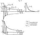
- a Leroy-Somer LSA 43.2 generator which is typical for small combined heat and power plants (“CHP"), has a maximum surge current of approx. 1 kA at a nominal current of 115 A (cf. Fig. 1A , 1B ).
- the semiconductor switch-off device disclosed here makes it possible to switch off this surge short-circuit current more or less hard in the event of an overshoot. This is particularly advantageous for a connection in the vicinity of poorly developed medium-voltage networks that cannot take up any further short-circuit current.
- Low voltage ride through is understood by the person skilled in the art to mean the - at least partially - tolerance of electrical generation units such as generators (or generally supply units such as also subordinate subnetworks to the respective higher-level network) with respect to short-term voltage dips:
- a generation / supply unit must not be in the event of voltage dips disconnect directly from the power grid, but must remain connected to the grid for a certain period of time and at least partially continue to feed in electricity.
- Brief voltage drops can occur, for example, as a result of network faults such as short circuits, earth faults or lightning strikes.
- the ability of decentralized generation systems or subordinate subnets to "low voltage ride through” prevents a large-scale network breakdown due to a domino effect of many smaller generator systems / subnetworks in the event of errors in the higher-level transmission network.
- Methods and devices for ensuring distance protection are also known to the person skilled in the art from the prior art, for example in the form of distance protection relays.
- the ability to deliver the overcurrent to the grid in a controlled manner is particularly useful in the transition phase of the grid conversion. This is especially true from the point at which large power plants can no longer provide enough electricity, to ensure network stability for the most part.
- the entire security concept could be reorganized; in existing ("historically grown") networks, there is no possibility of a completely new conception of network security.
- the present invention therefore also deals with the controlled provision of variably adjustable short-circuit currents in a low or medium voltage network.
- the object of the present invention is to solve the problems existing in the prior art by providing a method and a device for reliably detecting and limiting surge currents sufficiently quickly and thereby protecting power distribution networks from surge currents.
- the method and the device should also be inexpensive and reusable, that is to say that they can be switched on again, so that no distinction is made between real surge short-circuit currents and only uncritical network instabilities due to harmless mechanical switching processes ("flicker") must be taken.
- Another object of the present invention is not only to solve the problems in the prior art relating to the prevention of surge short-circuit currents (as described above), but also to provide a possibility for superordinate, critical operating or switched off power networks from subordinate power networks to start up again, ie to start / put into operation or to stabilize by providing a method and a device with which by feeding defined short-circuit currents from the lower-level network into the higher-level network and observing the behavior of the higher-level network, the higher-level network from within the lower level Can be put into operation or stabilized.
- system parameters such as voltage, current flow, phase position and the like
- the overall task is to control surge short-circuit currents in power grids, i.e. switch off or limit to a defined short-circuit current, and is made up of the two subtasks "switch off surge short-circuit currents" and "limit short-circuit currents / generate defined", each of the two sub-tasks already represents an inventive control of surge short-circuit currents, and thus a technical improvement network stability.
- the solution according to the invention for achieving the required high switching speeds is preferably based on semiconductors; although it naturally also has losses, similar to the standard solutions known in the prior art, this is not disadvantageous overall, since the multiple reversibility of the switching process means that the device according to the invention, ie the switch, operates without wear.
- switch here and in the following refers to the entire shutdown device according to the invention (synonym: “semiconductor shutdown device”); the actual switching semiconductor component, such as an IGBT or a MOSFET (m etal- o xide- s emiconductor F ield e ffect t Transistor) is referred to and to distinguish them as "semiconductor switching element” the anti-parallel arrangement of two such semiconductor switching elements as a "bi-directional semiconductor switch”.
- the switching semiconductor components are those components of the device that have the ability to switch off currents.
- control logic is to be provided, which according to the invention can preferably be implemented locally or provided by remote maintenance, and which, depending on the current operating state of the network, sets the current operating state of the device for controlling surge short-circuit currents as follows: Is the network stable in operation, is switched to the mode of switching off surge short-circuit currents, the network is out of operation or in a critical operating state, is switched to the mode of defined generation and supply of short-circuit currents.
- This task (the supply of defined short-circuit currents) is achieved by an arrangement of bidirectional switches and inductors which - when connected behind a synchronous or asynchronous generator - set a short-circuit current or any other current to a desired value through their control, and this current as well can hold for a predetermined time.
- the maximum possible time results from the component selection and can also be unlimited if necessary.
- the decisive factor here is, above all, the structural power loss of the components or the configuration of the cooling of the device. If this is designed in such a way that the maximum component temperature is not exceeded, unlimited operation, i.e. the maintenance of the short-circuit current for an unlimited period of time is possible.
- the device according to the invention for controlling surge short-circuit currents in power supply networks thus comprises both (sub) devices, individually or together; this also applies analogously to the two methods that are carried out with the relevant (sub) devices.
- non-mechanical switching elements include here and in the following both semiconductor switching elements such as, for example, IGBTs and MOSFETs, and also, for example, thyratrons or other non-semiconductor-based non-mechanical switching elements.
- step a) of the method described above can also include measuring the time profile of the current flow in the neutral conductor, so that the current flow in the neutral conductor can also be included in the following method steps.
- one would be three-phase three-phase network n 4 to integrate the neutral conductor in the process.
- the term “sum signal” not only includes a sum signal obtained as described above from at least two phase-specific individual measured values, which is proportional to the total current flow in the feed line, but also - depending on the embodiment of the invention - the phase-specific individual measured values. In this case, each individual phase must be monitored separately and switched off individually if the respective phase-specific limit value is exceeded.
- limit value in the context of the present disclosure not only includes a single limit value, as described above, with which the previously formed sum signal is compared, but also individual phase-specific limit values with which the phase-specific individual measured values are compared.
- the semiconductor switching elements connected in antiparallel to one another are so-called active semiconductor components, such as transistors, IGBTs, MOSFETs or diodes, the switching states of which can be influenced by electronic control signals or the current flow itself, and they are located in the current paths of each phase of the AC power distribution network .
- active semiconductor components such as transistors, IGBTs, MOSFETs or diodes, the switching states of which can be influenced by electronic control signals or the current flow itself, and they are located in the current paths of each phase of the AC power distribution network .
- IGBTs with an integrated free-wheeling diode the actual transistor and the diode are already arranged as required within the housing of the IGBT.
- the use of IGBTs is therefore particularly preferred.
- the arrangement in question can also be implemented by correspondingly interconnecting at least two transistors without an integrated free-wheeling diode and at least two separate diodes, the diodes also being connected in antiparallel to one another, i.e
- control of the anti-parallel interconnection Semiconductor components is basically always only the control of the transistors, since only these can be controlled by a separate control signal.
- the limit value of the sum signal is freely selected and specified, depending on how quickly the switch-off is to take place on the rising edge of the surge current. For example a value of U meas-sum can be specified as a limit value which corresponds to x the nominal current (x> 1), e.g. twice, three times, four times, five times, six times, seven times, eight times, nine times or ten times the nominal current.
- shutdown does not only mean the separation of the synchronous generator from the power supply system, but also the connection of at least one suitable consumer to absorb the current surge as “shutdown”. In this sense, “shutdown” is synonymous with "deriving excess current”.
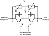
- suitable consumers can be, for example, adequately dimensioned resistors, which then - in a manner known per se to the person skilled in the art - the Fig. 9 varistors shown as examples are connected in parallel.
- the invention further comprises a switch-off device, which has at least two semiconductor switching elements arranged antiparallel to each other in each phase of the power network.
- semiconductor switching elements are preferably IGBT's ( "ate I nsulated G B Bipolar ransistors") to ensure that current flows that occur can be securely blocked, without the semiconductor switching elements in question are thereby excessively damaged . This ensures the desired reclosing capability of the invention, since the semiconductor switching elements can then carry out two or more switching operations before they may be due to safety / standard requirements and the like. U. need to be replaced.
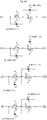
- Figure 2A shows a circuit diagram of such a component arrangement or interconnection according to the invention.
- Fig. 2B shows an example of a corresponding circuit diagram relating to a phase. It is within the scope of the invention to provide such a parallel arrangement of at least two semiconductor switching elements connected antiparallel to one another in the current path in question in one or more phases of the power network.
- An antiparallel arrangement or connection of two semiconductor switching elements is understood here to mean that, for example, when using IGBTs, the two emitter connections are connected to one another, and the collector connection of one IGBT is connected to the relevant phase of the generator (generator), and the Collector connection of the other IGBT with the relevant phase of the consumer (power grid).
- the two IGBTs are controlled via the gate connections.
- the monitoring of the individual currents in the network phases, or possibly in the individual current paths of the individual network phases, is carried out, for example, using current measuring transformers or by determining the voltage drop across the semiconductor switching elements.
- the detection of the currents and the consequent triggering (switch-off, opening) of the switches, if necessary, is so fast according to the invention that the delay due to the time required for the current detection and the switching is significantly less than 1 ⁇ s.
- the delay is preferably at most 600 ns, more preferably it is at most 300 ns and very particularly preferably it is at most 100 ns. This limits the short-circuit current delivered to the network to the nominal current.
- the semiconductor switching elements e.g. IGBTs or MOSFETs
- the semiconductor switching elements e.g. IGBTs or MOSFETs
- Incorrect tripping i.e. the suppression of the current flow and / or the triggering of a complete shutdown without a critical current surge actually occurring, is unproblematic in contrast to the Is limiters, since the switch works without wear (no new detonator or replacement of the device required), and after checking the network status can be switched on (switched on) or automatically switched on again.
- the switch-off device according to the invention can be used in low-voltage as well as in medium-voltage and high-voltage networks which are operated with AC voltage (multi-phase, preferably three-phase). It is preferably used in low and medium-voltage networks in the voltage range from 230 V to 50 kV, and very particularly preferably in low-voltage networks up to 690 V.
- the particularly preferred use in low-voltage networks results from the fact that network instabilities in low-voltage networks due to the connection of CHP units are particularly disadvantageous closely meshed Impact medium-voltage networks that are operated with approx. 10 kV, such as those operated in large cities or in densely built-up rural areas. This also applies to the extension of the object of the invention, namely the configuration as a current limiting device.
- the term “sum signal” in the context of the present disclosure includes not only a sum signal obtained as described above from at least two phase-specific individual measured values, which is proportional to the total current flow in the feed line, but also - depending on the embodiment of the invention - the phase-specific individual measured values.
- each individual phase must be monitored separately and switched off individually if the respective phase-specific limit value is exceeded.
- the "summation”, i.e. H. Formation of the "sum signal”, the exceeding of which leads to suppression of the surge short-circuit current, preferably by disconnecting all phases from the network, is then realized by monitoring and separating all the individual phases, which are essentially independent of one another.
- limit value in the context of the present disclosure not only includes a single limit value, as described above, with which the previously formed sum signal is compared, but also individual phase-specific limit values with which the phase-specific individual measured values are compared.
- All of the evaluation variants mentioned have in common that they detect when the current flow is too high, ie a surge short-circuit current occurs.
- the components required for the implementation of the various evaluation variants are essentially the same, but they are different in each case Arranged manner, which is known per se to the expert. With regard to current measurement, these are, for example, measuring resistors, measuring transformers, Hall probes, internal resistances of components, etc .; in terms of evaluation, for example, operational amplifiers, logic circuits, FPGA, CPLD, processors, etc.
- the non-mechanical switching elements are so-called “active” or “controllable” semiconductor components such as, for example, thyratrons or semiconductor switching elements, such as, for example, IGBTs and MOSFETs.
- the limit value of the sum signal U mess-sum mentioned in step c) is freely selected according to the invention, depending on the requirements for network stability; in particular, it also falls within the scope of the invention and its equivalents to adapt this limit value as required, that is to say to set it anew.
- the object of the invention further comprises a method as described above, which is characterized in that n has the value 3 or the value 4.
- the object of the invention further comprises a method as described above, which is characterized in that it is operated in a medium-voltage network in a voltage range from 1 kV to 50 kV or in a low-voltage network with an operating voltage between 50 V and 690 V.
- the object of the invention further comprises a method as described above, which is characterized in that it comprises, as a further sub-step dd), communication with at least one external network control module, this sub-step dd) taking place at least once after sub-step d) and either unidirectionally or bidirectionally takes place and step e) is then carried out partially or completely by the external network control module using the at least one-time communication.
- the control is, for example, so-called control boards for the respective non-mechanical control element or suitable, possibly programmable, microprocessors or computers or industrial controls such as PLC, SPSS or similar devices known to the person skilled in the art.
- the adjustable delay element results - in a manner known to the person skilled in the art - from the selection of the components for the device according to the invention from the operating parameters, in particular the switching times, the components or - likewise in a manner known to the person skilled in the art - by suitable programming of corresponding programmable components as they - if not exhaustive - have also already been mentioned above by way of example.
- the object of the invention further comprises an apparatus for performing the method as described above, and which are characterized is that, as a precaution, the device additionally has a fuse, it being known to the person skilled in the art what type and strength of fuse is suitable and how it is to be installed in the circuit.
- the object of the invention further comprises the use of a device as described above in a medium-voltage power network or in a low-voltage power network for suppressing surge short-circuit currents during the startup phase of at least one synchronous generator connected to the medium-voltage or low-voltage power network.
- the object of the invention in the configuration as a semiconductor current limiting device has, among other things, features described below, the above-described method and use variants of the semiconductor shutdown device also for the invention in the configuration as a semiconductor current limiting device are valid, ie both configurations of the object of the invention - semiconductor shutdown device and semiconductor current limiting device - can be combined with one another.
- the object of the invention further comprises a device for controlling surge short-circuit currents in power supply networks as described in the preceding paragraph, which is characterized in that the device further comprises at least one further additional bidirectional semiconductor switch ( 40 , 40 ' ), which is either between two phases or is located between each phase and the neutral conductor, and the semiconductor switching elements forming at least one additional bidirectional semiconductor switch are semiconductor switching elements selected from the list comprising IGBTs, MOSFETs, thyratrons.
- the invention further relates to a method for feeding defined surge short-circuit currents into a superordinate AC power distribution network, which is characterized in that at least one inductive element ( 30 ) and / or at least one semiconductor switching element ( 10, 10 ' ) with a frequency greater than 0 , 1 kHz, preferably greater than 1 kHz and particularly preferably greater than 15 kHz, which limits the current delivered to the higher-level network.
- the object of the invention further comprises a device for controlling surge short-circuit currents in power supply networks as described above, characterized in that the device further comprises at least one further additional bidirectional semiconductor switch ( 40 , 40 ' ) which has a free-wheeling path to another phase or to the Neutral conductor enables.
- the method according to the invention for controlling surge short-circuit currents is preferably carried out with the aid of the device according to the invention in a corresponding configuration.
- a generator with 3.8 kVA power is loaded with nominal current using ohmic high-performance resistors.
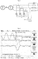
- an all-phase short-circuit is brought about and the current curves which occur are recorded by means of an LEM converter and represented by a digital storage oscilloscope of the Tektronix TDS2002B type (cf. Fig. 3).
- Fig. 4 shows an example of a recorded and evaluated oscillogram. The curves shown represent the highest short-circuit current I k determined in several runs. The peak that occurred never exceeded the read and marked value of 8 • I nominal . This ratio of I k / I nominal is therefore used as the maximum value for all further subsequent exemplary calculations.
- the person skilled in the art can use the data sheets available for all commercially available semiconductor components (for example IGBTs or MOSFETs) to select suitable semiconductor components which can be used to carry out the method according to the invention or to build the device according to the invention. Analogously to the semiconductor switching elements in a corresponding form, this also applies to the other semiconductor components and other electronic components to be used for the device in the various embodiments.
- semiconductor components for example IGBTs or MOSFETs
- the semiconductor switching elements are used in the non-clocked pass mode.
- the following key data are relevant, for example, although this list is not to be understood as restrictive: - V CES [V] maximum permissible collector-emitter voltage - I C [A] maximum permissible collector continuous current - I CRM [A] maximum permissible, temporary collector current - T vjmax [° C] maximum permissible semiconductor core temperature - V CE (sat) max [V] Collector-emitter voltage drop with full control - R th (jc) [° C / (kW)] Heat transfer resistance semiconductor core - IGBT housing - R th (ch) [° C / (kW)] Heat transfer resistance IGBT housing - heat sink
- IGBTs semiconductor switching elements
- Table 1 Two commercially available semiconductor switching elements (IGBTs) with their corresponding characteristic data, which can be used for the method and the device according to the invention, are mentioned as examples in Table 1.
- the aforementioned selection criteria for the power semiconductors apply analogously and by way of example also to the configuration of the object of the invention as a semiconductor current limiting device.
- Table 1 Semiconductor switching elements that can be used as examples according to the invention
- R th (jc) 0.11 ° C / W 0.067 ° C / W *) each at 80 ° C
- Table 2 Exemplary operating temperatures Operating status Semicron Fujielectric 20 kVA P nominal (normal operation) 98.64 ° C 123.77 ° C 20 kVA after shutdown (3x I nominal for 1 ms) 100.76 ° C 125.64 ° C 20 kVA "worst case” (8x I nominal for 9 ms) 118.44 ° C 142.94 ° C
- the Fujielectric® IGBT can be used without departing from the scope of the invention or its equivalents, but because of the high operating temperatures this is less advantageous than using the Semikron® IGBT's.
- the low thermal resistance of the Fuji-IGBT is also not sufficient to remove the heat generated in the component quickly enough. In the worst case, exceeding the maximum permissible junction temperature T vjmax - which is 150 ° C for this type - cannot be excluded with sufficient certainty. If this temperature is exceeded, the thermal destruction of the IGBT or at least its damage is inevitable.
- At least one coil ie an “inductor”
- a processor or an FPGA or a corresponding analog control which triggers the current limitation, ie the supply of the defined surge short-circuit current is accomplished.
- at least one switch of classic design can also be provided.
- the network monitoring methods usually known from the prior art, i.e.
- the detection of error situations / operating faults which can be used according to the invention in order subsequently to carry out switching / control / regulation processes according to the invention are known to the person skilled in the art, for example from the corresponding standard regulations.
- the trigger threshold to be selected, or the trigger range, must be flexibly determined based on two objectives.
- short, uncritical load peaks such as those that occur when switching on or at the start of feed-in, must not lead to switch-off.
- the maximum current actually flowing in the event of a fault that is to say when a surge short-circuit current occurs, is to be limited to a minimum.
- the compromise chosen here as an example for trigger values lies in the range between two and a half to three times the nominal generator current.
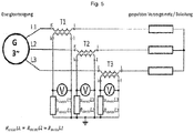
- the in Fig. 5 The measurement setup shown shows an example of a basic measurement setup for real-time current value acquisition.
- Other devices are known to the person skilled in the art and methods for current monitoring are known that can be used without departing from the scope of the invention or its equivalents.
- the flowing outer conductor currents ie the phase currents in phases L1, L2 and L3, are detected on the primary side by means of current transformers (for example current measuring transformers) T1, T2 and T3.
- current transformers for example current measuring transformers
- T1 T2 and T3 current measuring transformers
- Suitable electronic circuit arrangements for this purpose are known to the person skilled in the art and can be used according to the invention.
- the converters are short-circuited via three identical resistors (R mess ), which in turn are connected to each other in a star.
- R mess resistors
- the use of so-called "star circuits" and their advantageous use are known to the person skilled in the art.
- the flowing primary transformer current causes a secondary transformer current which has a fixed transmission ratio to the primary current and flows through the measuring resistors.
- the voltage drops occurring here at the resistors are recorded and fed to an evaluation circuit, which is shown in FIG Fig. 5 is not shown.
- Numerous evaluation circuits or measuring devices are known to the person skilled in the art from the prior art, which can be used without leaving the scope of the invention or its equivalents.
- the measuring resistors used should have the same values, if possible, in order to avoid measuring value falsifications between the individual outer conductors. If the measuring resistances have different values, this can be taken into account by means of appropriate correction factors and, if necessary, calibrations.
- the values of the resulting measuring voltages are directly proportional to the selected resistance values and can be calculated using Ohm's law.
- a voltage called "threshold voltage” drops in the order of magnitude of 0.6 to 0.7 V.
- This threshold voltage must be significantly exceeded by the measured values during nominal system operation in order to ensure the faultless switching function. If relatively small resistance values R mess of the order of a few milliohms are used, then the measured values U mess to be evaluated have relatively low voltage levels, which complicates the evaluation. This inevitably leads to further problems, since full rectification - especially in the voltage range from 0 to 0.7 V - is not guaranteed.
- the use of commercially available silicon diodes would therefore necessitate adjustments to the entire circuit in order to ensure reliable current measurement. It is therefore readily apparent to the person skilled in the art that the use of commercially available standard diodes falls within the scope of the invention and its equivalents, but is not a preferred embodiment.
- the three recorded measured values U mess-L1 , U mess-L2 and U mess-L3 are rectified using "active rectifiers".
- the core of these active rectifiers is formed by OPVs (so-called “operational amplifiers”) which have no threshold voltages. In this way, full rectification from 0 V is possible.
- Another advantage of this variant is the flexibility gained: On the one hand, the rectified measurement values can be raised or lowered to any voltage level within the OPV operating voltage ranges. On the other hand, in the measurement value acquisition - in direct comparison to the implementation with silicon diodes - no power is withdrawn, since OPVs are active components with a separate power supply. This minimizes falsifications of measurements.
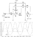
- Fig. 6 The preferred active rectification along with input and output variables of U mess-L1 is shown as an example (circuit diagram in the upper half, storage oscilloscope image in the lower half).
- a 50 Hz sine with an amplitude of 1 V peak was chosen as an exemplary input variable.
- auxiliary line drawn horizontal line at 0.0 V
- rectification is already proven from 0 V, completely without any threshold voltage occurring.
- the increased voltage level of the output variable compared to the input variable can also be seen.
- the use of exactly identical rectifiers for the individual measuring voltages U mess-L1 , U mess-L2 and U mess-L3 is particularly preferred.
- further embodiments falling within the scope of the invention and its equivalents also have different rectifiers and thus make it possible to monitor the individual phases independently of one another with different sensitivity.
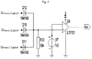
- the rectified measured values obtained as described above, preferably identically, are as in Fig. 7 described merged and decoupled from each other by means of diodes.
- the sum signal U mess-sum thus obtained which shows the voltage curve analogous to the output voltage of a B6 bridge circuit has, as is generally known to the person skilled in the art, a comparator (for example component "LT1721" in Fig. 7 ) fed.
- a comparator compares two input variables and makes a digital case distinction. If the input voltage is less than the comparison variable ( Fig. 7 : 1.5 V reference voltage source V7), the output level corresponds to almost 0 V. If the input voltage exceeds the reference voltage, the output level takes on the operating or supply voltage level of the comparator.
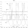
- Fig. 8 illustrates how it works using the exemplary simulation of an overload of L1.
- the voltage curves of U mess-L1 , U mess-L2 and U mess-L3 are shown , the rectified sum signal U mess-sum at the comparator input and the voltage curve at the comparator output (V [out]).
- the reference voltage used on the comparator is 7.5 V. It can be clearly seen that U mess-L1 has the highest amplitude due to the overload. After rectification and signal merging, there are slight overshoots in which the reference voltage is exceeded at certain points. Every time the comparator is exceeded, the "V (out)" curve takes on Fig.
- the switch-off device must either store a recognized network fault (i.e. a surge short-circuit current that has led to the switch-off) and remain switched off in order to then be switched on again by a higher-level network controller; in this case, the device must have at least one 1-bit error memory, which is reset when it is switched on again by the higher-level network controller.
- the method according to the invention or the device according to the invention comprises a control step or an internal control module (synonymously control) and has hardware and / or software implemented connection conditions when the method or the device itself fulfills the re-connection of the synchronous generator can make / cause
- an error memory is preferably used, which comprises at least 2 bit storage capacity.
- IGBTs are used as switches and "controlled” in order to implement the switching state "ON".
- the person skilled in the art knows how to control IGBTs or other non-mechanical switching elements so that current can flow.
- the collector-emitter path becomes conductive, the collector potential here having to be higher than that of the emitter.
- the currents to be switched are AC currents, the use of two IGBTs per outer conductor is essential. Both emitter connections are interconnected (anti-parallel Arrangement / connection) and due to the usually internally installed free-wheeling diode, the current paths result completely automatically.
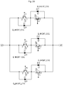
- Fig. 9 shows an example of a corresponding circuit diagram. Is that in Fig.
- varistors are provided parallel to the collector-emitter path of each IGBT (cf. Fig. 9 ).
- V CES maximum permissible collector-emitter voltage
- the varistor used should correspond approximately to this value.
- a usable type would be, for example, the Z80M112 from the manufacturer CKE®. The nominal breakdown voltage of this type is 1100 V ⁇ 10%. So the maximum voltage before the breakdown is 1210 V.
- the experimental data (e.g. currents, voltages, times, switching states) were recorded in all experiments / examples using a storage oscilloscope.
- the configuration of the object of the invention as a device for ensuring network stability in power supply networks by limiting a surge short-circuit current provides the following configuration options, which are described below by way of example with reference to the figures 11A-C are described in more detail.
- connection pins of the components can be selected at least in part, so that the numbers generated by the software of Connection pins of the same pins (eg emitter, collector, gate for transistors) can have different numbers in different drawings.
- the same reference symbols in different drawings in each case in connection with curved arrows always denote the same technical feature.
- Figure 11A shows the example of a three-phase power network, a first exemplary embodiment of the object of the invention for feeding a defined short-circuit current into a power network (phases L1 to L3, with the addition "ext" each identifying the external network side, ie the higher-level power network into which is fed ).
- the reference numerals 10 and 10 ' each denote the two semiconductor switching elements which are connected antiparallel to one another in one phase of the power network, in the present example with an integrated free-wheeling diode (not shown).
- This exemplary embodiment also has a varistor ( 20 ) connected in parallel with the respective semiconductor switching elements in each phase, as well as the additional inductance (coil) with the reference symbol 30 , which in this simplest embodiment variant already enables surge short-circuit currents to be limited and / or to be built up in a controlled manner.
- the processor or FPGA which is also required, or the corresponding analog control for triggering the current limitation, ie the supply of the defined surge short-circuit current, is not shown; the control signal lines required for this are connected to the connections of the semiconductor switching elements marked here with “2”.
- the principle of operation is such that the structure of the magnetic field in the inductance (coil 30 ) in the phase line creates a “buffer store” for the current fed in, from which, when disconnected from the mains, ie when the semiconductor switching elements 10, 10 'are opened, and the resulting breakdown of the magnetic field, the energy "flowing" out of the collapsing magnetic field is fed into the power network as a defined short-circuit current with decreasing intensity becomes.
- Corresponding software algorithms or analog control circuits with which this can be achieved according to the invention are known to the person skilled in the art and for the sake of clarity in the Figure 11A , 11B and 11C Not shown.
- Figure 11B also shows, using the example of a three-phase power network, a second exemplary embodiment of the object of the invention for feeding a defined short-circuit current into a power network (phases L1 to L3, the addition "ext” also feeding the external network side, ie the superordinate power network, into the here is marked).
- the reference numerals 10 and 10 ' here also denote the two semiconductor switching elements which are connected antiparallel to one another in a phase of the power network, in the present example also with an integrated free-wheeling diode (not shown).
- This exemplary embodiment also has the additional inductance (coil) 30 , which makes it possible to limit surge short-circuit currents and / or to build them up in a controlled manner, but does not require any varistors connected in parallel in the phases to the respective semiconductor switching elements 10, 10 ' , because the excess current is at this Embodiment not caught by consumers (eg varistors), but by means of appropriate control of the additional paired anti-parallel semiconductor switching elements 40, 40 ' in each of the two other phases, which still has capacity for the current flow.
- inductance (coil) 30 which makes it possible to limit surge short-circuit currents and / or to build them up in a controlled manner, but does not require any varistors connected in parallel in the phases to the respective semiconductor switching elements 10, 10 ' , because the excess current is at this Embodiment not caught by consumers (eg varistors), but by means of appropriate control of the additional paired anti-parallel semiconductor switching elements 40, 40 ' in each of the two other phases, which still has
- the necessary control of the semiconductor switching elements 40, 40 ' connected between the phases is also carried out according to the invention in a manner known from the prior art by means of a processor or FPGA or a corresponding analog control, the signal lines here also being connected to the connections marked "2" Semiconductor switching elements are connected.
- the processor or FPGA which is also required, or the corresponding analog control for triggering the current limitation, as well the redirection of the surge short-circuit current into another phase, ie the supply of the defined surge short-circuit current not shown.
- Figure 11C also shows, using the example of a three-phase power network, a third exemplary embodiment of the object of the invention for feeding a defined short-circuit current into a power network (phases L1 to L3, the addition "ext” here also feeding the external network side, ie the higher-level power network, into the is marked).
- the reference numerals 10 and 10 ' here also denote the two semiconductor switching elements which are connected antiparallel to one another in a phase of the power network, in the present example also with an integrated free-wheeling diode (not shown).
- This exemplary embodiment also has the additional inductance (coil) 30 , which makes it possible to limit surge short-circuit currents and / or to build them up in a controlled manner, but does not require any varistors connected in parallel in the phases to the respective semiconductor switching elements 10 , 10 ' , because the excess current is at this Embodiment not caught by consumers (eg varistors), but redirected by means of appropriate control of the additional pairs of anti-parallel semiconductor switching elements 40, 40 ' in the neutral conductor ("N”), which naturally still has capacity for the current flow.
- inductance (coil) 30 which makes it possible to limit surge short-circuit currents and / or to build them up in a controlled manner, but does not require any varistors connected in parallel in the phases to the respective semiconductor switching elements 10 , 10 ' , because the excess current is at this Embodiment not caught by consumers (eg varistors), but redirected by means of appropriate control of the additional pairs of anti-parallel semiconductor switching elements 40, 40
- the required control of the semiconductor switching elements 40, 40 ' connected between the phases and the neutral conductor is likewise carried out according to the invention in a manner known from the prior art by means of a processor or FPGA or a corresponding analog control, the signal lines here also being connected to the "2" marked connections of the semiconductor switching elements are connected.
- the processor or FPGA or the corresponding analog control for triggering the current limitation and the redirection of the surge short-circuit current into the neutral conductor is also not shown.
Landscapes
- Engineering & Computer Science (AREA)
- Power Engineering (AREA)
- Power Conversion In General (AREA)
- Control Of Eletrric Generators (AREA)
- Ac-Ac Conversion (AREA)
Applications Claiming Priority (1)
| Application Number | Priority Date | Filing Date | Title |
|---|---|---|---|
| DE102018121022.1A DE102018121022A1 (de) | 2018-08-28 | 2018-08-28 | Verfahren zur Unterdrückung von Stoßkurzschlußströmen sowie Halbleiter-Abschaltvorrichtung dafür |
Publications (4)
| Publication Number | Publication Date |
|---|---|
| EP3621168A2 true EP3621168A2 (fr) | 2020-03-11 |
| EP3621168A3 EP3621168A3 (fr) | 2020-08-26 |
| EP3621168B1 EP3621168B1 (fr) | 2026-01-21 |
| EP3621168C0 EP3621168C0 (fr) | 2026-01-21 |
Family
ID=67742260
Family Applications (1)
| Application Number | Title | Priority Date | Filing Date |
|---|---|---|---|
| EP19193354.8A Active EP3621168B1 (fr) | 2018-08-28 | 2019-08-23 | Procédé de vérification de courants de court-circuit ainsi que dispositif de vérification à semi-conducteur correspondant |
Country Status (2)
| Country | Link |
|---|---|
| EP (1) | EP3621168B1 (fr) |
| DE (1) | DE102018121022A1 (fr) |
Cited By (3)
| Publication number | Priority date | Publication date | Assignee | Title |
|---|---|---|---|---|
| CN115566664A (zh) * | 2022-09-09 | 2023-01-03 | 湖南工程学院 | 泄流器选址定容方法及相关设备 |
| RU2787974C1 (ru) * | 2022-04-11 | 2023-01-13 | Акционерное общество "ПРОТОН-ЭЛЕКТРОТЕКС" | Установка для определения класса силовых полупроводниковых приборов |
| CN116522739A (zh) * | 2023-06-29 | 2023-08-01 | 南昌科晨电力试验研究有限公司 | 一种基于数据分析的变压器短路冲击管控方法及系统 |
Families Citing this family (1)
| Publication number | Priority date | Publication date | Assignee | Title |
|---|---|---|---|---|
| CN116127163B (zh) * | 2023-04-14 | 2023-08-15 | 国网江西省电力有限公司电力科学研究院 | 一种抗干扰的电力变压器短路冲击分析系统及方法 |
Family Cites Families (10)
| Publication number | Priority date | Publication date | Assignee | Title |
|---|---|---|---|---|
| JPS52101451A (en) * | 1976-02-23 | 1977-08-25 | Toshiba Corp | Semiconductor breaker |
| US5216352A (en) * | 1990-11-29 | 1993-06-01 | Square D Company | Solid state current controlled interruption system |
| DE19801708C1 (de) * | 1998-01-17 | 1999-08-12 | E U S Gmbh | Kurzschlußstrombegrenzer für die Begrenzung von Fehlerströmen in einem elektrischen Energienetz |
| GB0103748D0 (en) * | 2001-02-15 | 2001-04-04 | Univ Northumbria Newcastle | A Hybrid fault current limiting and interrupting device |
| EP1993184B2 (fr) * | 2007-05-14 | 2024-04-24 | Siemens Gamesa Renewable Energy A/S | Procédé de démarrage d'au moins une partie d'une installation éolienne, installation éolienne et utilisation de l'installation éolienne |
| DE102008053822B3 (de) * | 2008-10-27 | 2010-06-17 | Siemens Aktiengesellschaft | Vorrichtung und Verfahren zur Speisung eines Abnehmernetzes mit der elektrischen Leistung eines Versorgungsnetzes |
| DE102011075567A1 (de) * | 2011-05-10 | 2012-11-15 | Siemens Aktiengesellschaft | Schalter, insbesondere Leistungsschalter für Niederspannungen |
| US9966206B1 (en) * | 2015-05-06 | 2018-05-08 | Google Llc | Circuit breakers with integrated safety, control, monitoring, and protection features |
| DE102016105662A1 (de) * | 2016-03-29 | 2017-10-05 | Wobben Properties Gmbh | Verfahren zum Einspeisen elektrischer Leistung in ein elektrisches Versorgungsnetz mit einem Windpark sowie Windpark |
| PL3568915T3 (pl) * | 2017-01-13 | 2023-10-30 | Siemens Energy AS | Zespół i sposób przełączania zasilania prądem stałym |
-
2018
- 2018-08-28 DE DE102018121022.1A patent/DE102018121022A1/de active Pending
-
2019
- 2019-08-23 EP EP19193354.8A patent/EP3621168B1/fr active Active
Cited By (4)
| Publication number | Priority date | Publication date | Assignee | Title |
|---|---|---|---|---|
| RU2787974C1 (ru) * | 2022-04-11 | 2023-01-13 | Акционерное общество "ПРОТОН-ЭЛЕКТРОТЕКС" | Установка для определения класса силовых полупроводниковых приборов |
| CN115566664A (zh) * | 2022-09-09 | 2023-01-03 | 湖南工程学院 | 泄流器选址定容方法及相关设备 |
| CN116522739A (zh) * | 2023-06-29 | 2023-08-01 | 南昌科晨电力试验研究有限公司 | 一种基于数据分析的变压器短路冲击管控方法及系统 |
| CN116522739B (zh) * | 2023-06-29 | 2023-09-26 | 南昌科晨电力试验研究有限公司 | 一种基于数据分析的变压器短路冲击管控方法及系统 |
Also Published As
| Publication number | Publication date |
|---|---|
| EP3621168B1 (fr) | 2026-01-21 |
| DE102018121022A1 (de) | 2020-03-05 |
| EP3621168C0 (fr) | 2026-01-21 |
| EP3621168A3 (fr) | 2020-08-26 |
Similar Documents
| Publication | Publication Date | Title |
|---|---|---|
| EP1922803B1 (fr) | Dispositif de transmission d'energie electrique | |
| EP3257147B1 (fr) | Ensemble convertisseur et procédé de protection contre les court-circuits dudit ensemble convertisseur | |
| EP3574515B1 (fr) | Disjoncteur basse tension | |
| DE102012109012B4 (de) | Schaltungsanordnung für ein Solarkraftwerk mit einer Gleichspannungsquelle für eine Offsetspannung | |
| EP3206286A1 (fr) | Commande de grille operée avec surtension pour conduire et commuter des courants de choc dans des commutateurs igbt | |
| EP2100368A1 (fr) | Éléments de protection semi-conducteurs pour maîtriser des courts-circuits côté cc dans des convertisseurs indirects de tension | |
| EP3379725A1 (fr) | Procédé de commande d'un commutateur à courant continu, commutateur à courant continu et système de tension continue | |
| DE19600547A1 (de) | Umrichterschutzgerät für elektrisches Netz | |
| DE102014209729A1 (de) | Vorrichtung zur kontaktlosen Übertragung von Energie | |
| EP3059828A1 (fr) | Dispositif et procede de detection de courant differentiel | |
| EP3743980A1 (fr) | Dispositif de commutation | |
| EP2974021B1 (fr) | Interrupteur haute puissance à courant continu | |
| WO1997036373A1 (fr) | Appareil de commutation electronique de derivation | |
| DE102021210828A1 (de) | Schutzschaltgerät und Verfahren | |
| EP3891890A1 (fr) | Interrupteur électronique fiable | |
| EP3621168B1 (fr) | Procédé de vérification de courants de court-circuit ainsi que dispositif de vérification à semi-conducteur correspondant | |
| EP3874571A1 (fr) | Circuit à impulsions pour la fourniture d'un courant de défaut dans un réseau d'alimentation en énergie à tension continue | |
| EP3783783A1 (fr) | Agencement de régulation d'un flux de puissance dans un réseau à tension alternative et procédé de protection de l'agencement | |
| EP3593434A1 (fr) | Procédé et agencement pour produire un signal de déclenchement pour un interrupteur ccht | |
| WO2013117385A2 (fr) | Alimentation électrique | |
| DE102021208466B4 (de) | Trennschaltereinheit | |
| DE102013109714A1 (de) | Verfahren zum Betreiben einer elektrischen Schaltung sowie elektrische Schaltung | |
| EP2479859B1 (fr) | Dispositif de commutation de sécurité | |
| WO2014154233A1 (fr) | Boîte de jonction pour le raccordement électrique d'une pluralité de générateurs photovoltaïques et installation de production d'énergie photovoltaïque | |
| DE102016116093A1 (de) | Schaltungsanordnung zum Schutz von an einem mehrphasigen Netz angeschlossenen Verbrauchern mit Unter- und Überspannungsabschaltfunktion |
Legal Events
| Date | Code | Title | Description |
|---|---|---|---|
| PUAI | Public reference made under article 153(3) epc to a published international application that has entered the european phase |
Free format text: ORIGINAL CODE: 0009012 |
|
| STAA | Information on the status of an ep patent application or granted ep patent |
Free format text: STATUS: THE APPLICATION HAS BEEN PUBLISHED |
|
| AK | Designated contracting states |
Kind code of ref document: A2 Designated state(s): AL AT BE BG CH CY CZ DE DK EE ES FI FR GB GR HR HU IE IS IT LI LT LU LV MC MK MT NL NO PL PT RO RS SE SI SK SM TR |
|
| AX | Request for extension of the european patent |
Extension state: BA ME |
|
| PUAL | Search report despatched |
Free format text: ORIGINAL CODE: 0009013 |
|
| AK | Designated contracting states |
Kind code of ref document: A3 Designated state(s): AL AT BE BG CH CY CZ DE DK EE ES FI FR GB GR HR HU IE IS IT LI LT LU LV MC MK MT NL NO PL PT RO RS SE SI SK SM TR |
|
| AX | Request for extension of the european patent |
Extension state: BA ME |
|
| RIC1 | Information provided on ipc code assigned before grant |
Ipc: H02H 9/00 20060101AFI20200718BHEP Ipc: H02H 3/02 20060101ALI20200718BHEP Ipc: H02J 3/00 20060101ALI20200718BHEP |
|
| STAA | Information on the status of an ep patent application or granted ep patent |
Free format text: STATUS: REQUEST FOR EXAMINATION WAS MADE |
|
| 17P | Request for examination filed |
Effective date: 20210226 |
|
| RBV | Designated contracting states (corrected) |
Designated state(s): AL AT BE BG CH CY CZ DE DK EE ES FI FR GB GR HR HU IE IS IT LI LT LU LV MC MK MT NL NO PL PT RO RS SE SI SK SM TR |
|
| STAA | Information on the status of an ep patent application or granted ep patent |
Free format text: STATUS: EXAMINATION IS IN PROGRESS |
|
| 17Q | First examination report despatched |
Effective date: 20230331 |
|
| GRAP | Despatch of communication of intention to grant a patent |
Free format text: ORIGINAL CODE: EPIDOSNIGR1 |
|
| STAA | Information on the status of an ep patent application or granted ep patent |
Free format text: STATUS: GRANT OF PATENT IS INTENDED |
|
| INTG | Intention to grant announced |
Effective date: 20250818 |
|
| GRAS | Grant fee paid |
Free format text: ORIGINAL CODE: EPIDOSNIGR3 |
|
| GRAA | (expected) grant |
Free format text: ORIGINAL CODE: 0009210 |
|
| STAA | Information on the status of an ep patent application or granted ep patent |
Free format text: STATUS: THE PATENT HAS BEEN GRANTED |
|
| AK | Designated contracting states |
Kind code of ref document: B1 Designated state(s): AL AT BE BG CH CY CZ DE DK EE ES FI FR GB GR HR HU IE IS IT LI LT LU LV MC MK MT NL NO PL PT RO RS SE SI SK SM TR |
|
| REG | Reference to a national code |
Ref country code: CH Ref legal event code: F10 Free format text: ST27 STATUS EVENT CODE: U-0-0-F10-F00 (AS PROVIDED BY THE NATIONAL OFFICE) Effective date: 20260121 |
|
| REG | Reference to a national code |
Ref country code: DE Ref legal event code: R096 Ref document number: 502019014303 Country of ref document: DE |
|
| REG | Reference to a national code |
Ref country code: IE Ref legal event code: FG4D Free format text: LANGUAGE OF EP DOCUMENT: GERMAN |
|
| U01 | Request for unitary effect filed |
Effective date: 20260220 |
|
| U07 | Unitary effect registered |
Designated state(s): AT BE BG DE DK EE FI FR IT LT LU LV MT NL PT RO SE SI Effective date: 20260325 |