EP3624177A1 - Procédé d'encapsulation de puce - Google Patents
Procédé d'encapsulation de puce Download PDFInfo
- Publication number
- EP3624177A1 EP3624177A1 EP18914930.5A EP18914930A EP3624177A1 EP 3624177 A1 EP3624177 A1 EP 3624177A1 EP 18914930 A EP18914930 A EP 18914930A EP 3624177 A1 EP3624177 A1 EP 3624177A1
- Authority
- EP
- European Patent Office
- Prior art keywords
- wafer
- chip
- insulating
- depositing
- fabricating
- Prior art date
- Legal status (The legal status is an assumption and is not a legal conclusion. Google has not performed a legal analysis and makes no representation as to the accuracy of the status listed.)
- Withdrawn
Links
Images




Classifications
-
- H—ELECTRICITY
- H10—SEMICONDUCTOR DEVICES; ELECTRIC SOLID-STATE DEVICES NOT OTHERWISE PROVIDED FOR
- H10W—GENERIC PACKAGES, INTERCONNECTIONS, CONNECTORS OR OTHER CONSTRUCTIONAL DETAILS OF DEVICES COVERED BY CLASS H10
- H10W74/00—Encapsulations, e.g. protective coatings
- H10W74/01—Manufacture or treatment
- H10W74/014—Manufacture or treatment using batch processing
-
- H—ELECTRICITY
- H10—SEMICONDUCTOR DEVICES; ELECTRIC SOLID-STATE DEVICES NOT OTHERWISE PROVIDED FOR
- H10P—GENERIC PROCESSES OR APPARATUS FOR THE MANUFACTURE OR TREATMENT OF DEVICES COVERED BY CLASS H10
- H10P54/00—Cutting or separating of wafers, substrates or parts of devices
-
- H—ELECTRICITY
- H10—SEMICONDUCTOR DEVICES; ELECTRIC SOLID-STATE DEVICES NOT OTHERWISE PROVIDED FOR
- H10W—GENERIC PACKAGES, INTERCONNECTIONS, CONNECTORS OR OTHER CONSTRUCTIONAL DETAILS OF DEVICES COVERED BY CLASS H10
- H10W72/00—Interconnections or connectors in packages
- H10W72/01—Manufacture or treatment
- H10W72/019—Manufacture or treatment of bond pads
-
- H—ELECTRICITY
- H10—SEMICONDUCTOR DEVICES; ELECTRIC SOLID-STATE DEVICES NOT OTHERWISE PROVIDED FOR
- H10W—GENERIC PACKAGES, INTERCONNECTIONS, CONNECTORS OR OTHER CONSTRUCTIONAL DETAILS OF DEVICES COVERED BY CLASS H10
- H10W72/00—Interconnections or connectors in packages
- H10W72/01—Manufacture or treatment
- H10W72/0198—Manufacture or treatment batch processes
-
- H—ELECTRICITY
- H10—SEMICONDUCTOR DEVICES; ELECTRIC SOLID-STATE DEVICES NOT OTHERWISE PROVIDED FOR
- H10W—GENERIC PACKAGES, INTERCONNECTIONS, CONNECTORS OR OTHER CONSTRUCTIONAL DETAILS OF DEVICES COVERED BY CLASS H10
- H10W72/00—Interconnections or connectors in packages
- H10W72/90—Bond pads, in general
-
- H—ELECTRICITY
- H10—SEMICONDUCTOR DEVICES; ELECTRIC SOLID-STATE DEVICES NOT OTHERWISE PROVIDED FOR
- H10W—GENERIC PACKAGES, INTERCONNECTIONS, CONNECTORS OR OTHER CONSTRUCTIONAL DETAILS OF DEVICES COVERED BY CLASS H10
- H10W74/00—Encapsulations, e.g. protective coatings
- H10W74/10—Encapsulations, e.g. protective coatings characterised by their shape or disposition
- H10W74/111—Encapsulations, e.g. protective coatings characterised by their shape or disposition the semiconductor body being completely enclosed
- H10W74/129—Encapsulations, e.g. protective coatings characterised by their shape or disposition the semiconductor body being completely enclosed forming a chip-scale package [CSP]
-
- H—ELECTRICITY
- H10—SEMICONDUCTOR DEVICES; ELECTRIC SOLID-STATE DEVICES NOT OTHERWISE PROVIDED FOR
- H10W—GENERIC PACKAGES, INTERCONNECTIONS, CONNECTORS OR OTHER CONSTRUCTIONAL DETAILS OF DEVICES COVERED BY CLASS H10
- H10W72/00—Interconnections or connectors in packages
- H10W72/90—Bond pads, in general
- H10W72/941—Dispositions of bond pads
- H10W72/944—Dispositions of multiple bond pads
Definitions
- the present application relates to the field of chips, and in particular, to a chip packaging method.
- fabricating a semiconductor device may be divided into three steps: chip design, wafer fabrication (front end of the line), and packaging and testing (back end of the line).
- packaging mainly plays a role in bringing out pins of a chip and isolating the chip from the exterior.
- a boundary between back-end packaging and front-end fabricating is gradually blurred, which means that a wafer foundry may also involves some packaging processes.
- wafer level chip scale packaging may effectively reduce a volume of a packaged surface mounted device (Surface Mounted Device, SMD) while ensuring low cost.
- SMD Surface Mounted Device
- WLCSP has poor sealing performance and a back surface and a side surface of a chip are not protected.
- eWLCSP Encapsulated WLCSP
- the eWLCSP requires to first process a wafer fabricated at a front end in a form of WLCSP and cut it into chips; then arrange the chips that pass the test on a carrier at a certain interval; encapsulate all the chips with a plastic packaging material and then cure them; and finally, perform secondary cutting to obtain discrete devices.
- This technology may effectively protect six surfaces of the chip, but the cost is relatively high.
- Another technique is to use an injection mold to cover a plastic packaging material at a front surface and in a pre-formed scribe line of a wafer fabricated at a front end, and then combine a redistribution layer (Redistribution Layer, RDL) process, thinning of a back surface of the wafer and back surface plastic packaging to realize complete package of six surfaces of the chip.
- RDL redistribution Layer
- the present application provides a chip packaging method, which could achieve insulation protection for a side surface of a wafer-level chip utilizing a semiconductor front-end process, a step of packaging a single chip at a back end is omitted, cost is lower, and a chip volume is smaller.
- a chip packaging method including: fabricating an insulating band on a scribe line of a wafer, where a front surface of the wafer is provided with a plurality of independent chip regions, a portion between any two adjacent chip regions of the plurality of chip regions is the scribe line, and between the any two adjacent chip regions, a depth of the insulating band is greater than or equal to a thickness of the chip region and less than or equal to a thickness of the wafer, and a width of the insulating band is less than or equal to a width of the scribe line; fabricating an insulating layer on an upper surface of the wafer; fabricating a plurality of holes on the insulating layer above each of the plurality of chip regions to expose each chip region; depositing a conductive material in the plurality of holes to form a plurality of bonding pads; and thinning a back surface of the wafer to obtain a packaged discrete device for the each chip region.
- the fabricating the insulating band on the scribe line of the wafer includes: fabricating, on the scribe line, a trench surrounding the each chip region; and depositing an insulating material on an inner surface of the trench, such that the trench deposited the insulating material forms the insulating band, where a depth of the trench deposited the insulating material is greater than or equal to the thickness of the each chip region; and the thinning the back surface of the wafer to obtain the packaged discrete device for the each chip region includes: thinning the back surface of the wafer to separate the plurality of chip regions to obtain the packaged discrete device for the each chip region.
- the fabricating the insulating band on the scribe line of the wafer includes: fabricating, on the scribe line, a trench surrounding the each chip region, where a depth of the trench is greater than or equal to a thickness of a surrounded chip region and less than or equal to a thickness of the wafer; depositing an insulating material inside the trench to form the insulating band; the thinning the back surface of the wafer to obtain the packaged discrete device for the each chip region includes: thinning the back surface of the wafer to expose the insulating band, and dicing along the insulating band to obtain the packaged discrete device for the each chip region.
- the fabricating, on the scribe line, the trench surrounding the each chip region includes: fabricating the trench on the scribe line by means of at least one of dry etching, wet etching and mechanical cutting.
- the fabricating the trench on the scribe line by means of at least one of dry etching, wet etching and mechanical cutting includes: depositing a first protective layer on the upper surface of the wafer; fabricating a first window on the first protective layer above the scribe line; and etching the wafer in a first chemical solution to obtain the trench at the first window.
- the depositing the first protective layer on the upper surface of the wafer includes: depositing a silicon nitride layer as the first protective layer on the upper surface of the wafer by means of plasma assisted deposition, where the first chemical solution is any one of a potassium hydroxide solution, a sodium hydroxide (NaOH) solution, a tetramethylammonium hydroxide (TMAH) solution and a mixed solution containing hydrofluoric acid and nitric acid HNA.
- the first chemical solution is any one of a potassium hydroxide solution, a sodium hydroxide (NaOH) solution, a tetramethylammonium hydroxide (TMAH) solution and a mixed solution containing hydrofluoric acid and nitric acid HNA.
- the trench is trapezoidal with a bottom width smaller than an upper width; or the trench is rectangular with a bottom width equal to an upper width.
- the fabricating the insulating band on the scribe line of the wafer includes: converting a portion of the scribe line surrounding the each chip region into a porous silicon region by electrochemical etching, where the porous silicon region is the insulating band; and the thinning the back surface of the wafer to obtain the packaged discrete device for the each chip region includes: thinning the back surface of the wafer to expose the insulating band, and dicing along the insulating band to obtain the packaged discrete device for the each chip region.
- the converting the portion of the scribe line surrounding the each chip region into the porous silicon region by the electrochemical etching includes: depositing a second protective layer on the upper surface of the wafer; fabricating a second window on the second protective layer above the scribe line; and placing the wafer in a second chemical solution to obtain the porous silicon region at the second window by the electrochemical etching.
- the depositing the second protective layer on the upper surface of the wafer includes: depositing a fluoropolymer layer as the second protective layer on the upper surface of the wafer by means of plasma assisted deposition, where the second chemical solution is a mixed solution containing hydrofluoric acid.
- the wafer in another implementation manner of the first aspect, includes an insulating layer, the insulating layer is disposed below the each chip region, and the insulating band and the insulating layer are connected.
- the thinning the back surface of the wafer to obtain the packaged discrete device for the each chip region includes: thinning the back surface of the wafer to expose the insulating layer, and dicing along the insulating band to obtain the packaged discrete device for the each chip region.
- the thinning the back surface of the wafer includes: thinning the back surface of the wafer by means of at least one of lapping, grinding, chemical mechanical polish, dry polishing, electrochemical etching, wet etching, plasma assisted chemical etching and atmospheric downstream plasma etching.
- the fabricating the insulating layer on the upper surface of the wafer includes: depositing an insulating material on the upper surface of the wafer to form the insulating layer.
- the depositing the insulating material includes: depositing the insulating material by means of at least one of physical vapor deposition, chemical vapor deposition, spraying and spin-coating.
- the insulating material includes at least one of a silicon oxide, a silicon nitride, and a polymer.
- the depositing the conductive material includes: depositing the conductive material by means of at least one of atomic layer deposition, physical vapor deposition, metal-organic chemical vapor deposition, evaporation, and electroplating.
- the conductive material includes at least one of heavily doped polysilicon, carbon-based material, metal, and titanium nitride.
- a chip packaging method including: fabricating an insulating band on a scribe line of a wafer, where a front surface of the wafer is provided with a plurality of independent chip regions, a portion between any two adjacent chip regions of the plurality of chip regions is the scribe line, and between the any two adjacent chip regions, a depth of the insulating band is greater than or equal to a thickness of the chip region and less than or equal to a thickness of the wafer, and a width of the insulating band is less than or equal to a width of the scribe line; fabricating a first insulating layer on an upper surface of the wafer; fabricating a first window on the first insulating layer above each of the plurality of chip regions to expose each chip region; depositing a conductive material in the first window to form a first bonding pad of the each chip; and thinning a back surface of the wafer to expose the insulating band; and depositing a conductive material on a back surface of a
- the depositing the conductive material on the back surface of the thinned wafer to form the second bonding pad for the each chip region includes: depositing an insulating material on the back surface of the thinned wafer to form a second insulating layer; fabricating, on the second insulating layer below the each chip region, a second window to expose the each chip region; and depositing a conductive material in the second window to form the second bonding pad of the each chip.
- a material of the first insulating layer is the same as that of the second insulating layer.
- the fabricating the insulating band on the scribe line of the wafer includes: fabricating, on the scribe line, a trench surrounding the each chip region, where a depth of the trench is greater than or equal to a thickness of a surrounded chip region and less than or equal to a thickness of the wafer; and depositing an insulating material inside the trench to form the insulating band.
- the fabricating, on the scribe line, the trench surrounding the each chip region includes: fabricating the trench on the scribe line by means of at least one of dry etching, wet etching and mechanical cutting.
- the fabricating the trench on the scribe line by means of at least one of dry etching, wet etching and mechanical cutting includes: depositing a first protective layer on the upper surface of the wafer; fabricating a third window on the first protective layer above the scribe line; and etching the wafer in a first chemical solution to obtain the trench at the third window.
- the depositing the first protective layer on the upper surface of the wafer includes: depositing a silicon nitride layer as the first protective layer on the upper surface of the wafer by means of plasma assisted deposition, where the first chemical solution is any one of a potassium hydroxide solution, a sodium hydroxide (NaOH) solution, a tetramethylammonium hydroxide (TMAH) solution and a mixed solution containing hydrofluoric acid and nitric acid HNA.
- the first chemical solution is any one of a potassium hydroxide solution, a sodium hydroxide (NaOH) solution, a tetramethylammonium hydroxide (TMAH) solution and a mixed solution containing hydrofluoric acid and nitric acid HNA.
- the trench is trapezoidal with a bottom width smaller than an upper width; or the trench is rectangular with a bottom width equal to an upper width.
- the fabricating the insulating band on the scribe line of the wafer includes: converting a portion of the scribe line surrounding the each chip region into a porous silicon region by electrochemical etching, where the porous silicon region is the insulating band.
- the converting the portion of the scribe line surrounding the each chip region into the porous silicon region by the electrochemical etching includes: depositing a second protective layer on the upper surface of the wafer; fabricating a fourth window on the second protective layer above the scribe line; and placing the wafer in a second chemical solution to obtain the porous silicon region at the fourth window by the electrochemical etching.
- the depositing the second protective layer on the upper surface of the wafer includes: depositing a fluoropolymer layer as the second protective layer on the upper surface of the wafer by means of plasma assisted deposition, where the second chemical solution is a mixed solution containing hydrofluoric acid.
- a material of the first bonding pad is the same as that of the second bonding pad.
- the thinning the back surface of the wafer includes: thinning the back surface of the wafer by means of at least one of lapping, grinding, chemical mechanical polish, dry polishing, electrochemical etching, wet etching, plasma assisted chemical etching and atmospheric downstream plasma etching.
- the fabricating the insulating layer on the upper surface of the wafer includes: depositing an insulating material on the upper surface of the wafer to form the insulating layer.
- the depositing the insulating material includes: depositing the insulating material by means of at least one of physical vapor deposition, chemical vapor deposition, plasma assisted deposition, spraying and spin-coating.
- the insulating material includes at least one of a silicon oxide, a silicon nitride, and a polymer.
- the depositing the conductive material includes: depositing the conductive material by means of at least one of atomic layer deposition, physical vapor deposition, metal-organic chemical vapor deposition, evaporation, and electroplating.
- the conductive material includes at least one of heavily doped polysilicon, carbon-based material, metal, and titanium nitride.
- the insulating band is grid-shaped as a whole, where the scribe lines on the wafer are grid-shaped as a whole, the chip regions are located between the grids, and corresponding grid-shaped insulating bands may be formed at corresponding positions of the grid-shaped scribe lines.
- an insulation protection method for a side surface of a wafer-level chip in a semiconductor front-end process is achieved by fabricating a trench surrounding chips and having an insulating material therein, or by fabricating a grid-shaped porous silicon region surrounding chips, so that a step of packaging a single chip at a back end is omitted, cost is lower, and a chip volume is smaller, thereby resolving a contradiction of insulation protection for a side surface of a semiconductor discrete device and complicated packaging procedures at the back end.
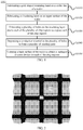
- FIG. 1 shows a schematic flowchart of a chip packaging method 1000 according to an embodiment of the present application.
- the method 1000 includes: S1010, fabricating an insulating band on a scribe line of a wafer, where a front surface of the wafer is provided with a plurality of independent chip regions, a portion between any two adjacent chip regions of the plurality of chip regions is the scribe line, and between the any two adjacent chip regions, a depth of the insulating band is greater than or equal to a thickness of the chip region and less than or equal to a thickness of the wafer, and a width of the insulating band is less than or equal to a width of the scribe line; S 1020, fabricating an insulating layer on an upper surface of the wafer; S1030, fabricating a plurality of holes on the insulating layer above each of the plurality of chip regions to expose each of the chip regions; S1040, depositing a conductive material in the plurality of holes to form a plurality of bond
- a wafer in an embodiment of the present application may be the wafer 100 shown in FIGS. 2 and 3
- FIG. 2 shows a top view of a wafer 100 according to an embodiment of the present application
- FIG. 3 shows a cross-sectional view of a wafer 100 according to an embodiment of the present application.
- the wafer 100 includes a plurality of independent chip regions 110 that may be uniformly arranged as shown in FIG. 2 , that is, horizontal distances between two adjacent chip regions 110 in a horizontal direction are the same, vertical distances between two adjacent chip regions 110 in a vertical direction are the same, and the horizontal distances and the vertical distances are the same.
- the chip regions 110 on the wafer 100 may also be nonuniformly arranged, for example, horizontal distances are different, or vertical distances are different, or the horizontal distances differ from the vertical distances, and the embodiment of the present application is not limited thereto.
- a thickness of each of the chip regions 110 on the wafer 100 is less than a thickness of the wafer 100.
- a thickness of each of the chip regions 110 may be set according to a thickness of a chip to be packaged or a type of a chip to be packaged.
- the thickness of the chip region 110 in the embodiment of the present application refers to an effective thickness of the chip region 100 in practical application.
- a region on the wafer 100 other than the chip region 110 is a scribe line 120, that is, the scribe line 120 is a region between two adjacent chip regions 110.
- the scribe line 120 is grid-shaped, and correspondingly, an insulating band fabricated on the scribe line 120 of the wafer 100 is also grid-shaped.
- the insulating band is fabricated on the scribe line 120 of the wafer 100.
- the insulating band may be fabricated in various ways, and the chip may be packaged according to different insulating bands.
- fabricating the insulating band may include fabricating a trench on the scribe line 120 and depositing an insulating material in the trench to form the insulating band; or by electrochemical etching or other manners, converting a portion of a region of the scribe line 120 into a porous silicon region or an insulating region made of other materials as an insulating band.
- a first embodiment of the chip packaging method 1000 of Embodiment 1 will be described in detail with reference to FIGS. 4 to 8 .
- the first embodiment includes the following steps (steps 11.1-11.5).
- Step 11.1 a trench 202 surrounding each of chip regions 110 is fabricated on a scribe line 120.
- a depth of the trench is greater than a thickness of the chip region 110 and less than a thickness of the wafer 100, and a width of the trench 202 is less than or equal to a width of the scribe line 120, where the trench 202 may be as shown in FIG. 4 .
- a side section of the trench 202 being a trapezoid whose lower part is narrower and upper part is wider (also referred to as an inverted trapezoid) is taken as an example.
- a side section of the trench 202 may be any pattern, including regular and irregular patterns, for example, the trench 202 may be a rectangle with an upper width equal to a lower width, or may also be an arc, and the embodiment of the present application is not limited thereto.
- the width of the trench 202 may refer to a maximum width of the side section of the trench 202; for example, as shown in FIG. 4 , a maximum width of the trench is an uppermost opening of the trench 202, and the width is less than or equal to the width of the scribe line 120.
- the trench 202 may be fabricated on the scribe line 120 by means of at least one of dry etching, wet etching and mechanical cutting.
- a first protective layer 201 may be first deposited on an upper surface of a wafer 100, for example, by means of plasma assisted deposition, a silicon nitride layer is deposited on a front surface of the wafer 100 as the first protective layer 201; a first window that surrounds the chip region 110 is fabricated on a corresponding first protective layer above the scribe line 120, for example, a window is opened by photolithography in a region located above the scribe line 120 in the first protective layer 201; the wafer 100 is etched in a first chemical solution to obtain the trench 202 surrounding each of the chip regions 110 at the first window, where the first chemical solution may be any one of a potassium hydroxide solution, a sodium hydroxide (NaOH) solution, a tetramethylammonium hydroxide (NaOH) solution, a tetramethylammonium hydro
- an insulating material is deposited on an inner surface of the trench 202, and the trench deposited the insulating material may form an insulating band 203; a depth of the trench deposited the insulating material is greater than or equal to a thickness of the chip region 110; at the same time, an insulating layer 204 is also fabricated on an upper surface of the wafer 100, for example, an insulating material is deposited on the upper surface of the wafer 100 to form the insulating layer 204.
- depositing the insulating material in the embodiment of the present application for example, depositing the insulating material to form the insulating band 203, for another example, depositing the insulating material to form the insulating layer 204, all of these may be performed by at least one of the following manners, and various processes of depositing the insulating material may be the same or different.
- the insulating material includes a silicon nitride or a silicon oxide grown by physical vapor deposition (Physical Vapor Deposition, PVD) or chemical vapor deposition (Chemical Vapor Deposition, CVD), such as unpoded silicon glass (Undoped Silicon Glass, USG), or a silicon oxide converted by tetraethyl orthosilicate (Tetraethyl Orthosilicate, TEOS), or the like.
- PVD Physical Vapor Deposition
- CVD chemical vapor deposition
- unpoded silicon glass Undoped Silicon Glass, USG
- silicon oxide converted by tetraethyl orthosilicate Tetraethyl Orthosilicate, TEOS
- the insulating material includes various types of sprayed or spin-coated polymers, such as polyimide (Polyimide), parylene (Parylene), benzocyclobutene (BCB) or the like; alternatively, the insulating material also includes a spin on glass (spin on glass, SOG), that is, amorphous phase silicon oxide obtained by spin-coating or spraying a silicide-containing solution on a silicon wafer, then performing heating to remove a solvent, and conducting curing. One or more layers of the insulating material may be deposited. The insulating band 203 and the insulating layer 204 may be simultaneously formed in a same process.
- the insulating material is deposited in the trench 202 to form the insulating band 203, the insulating material only covers the surface of the trench to form a concave insulating layer having a certain thickness, and a depth of a concave portion of the concave insulating layer is still greater than or equal to the thickness of the chip region 110.
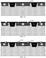
- Step 11.3 a plurality of holes are fabricated on the insulating layer 204 above each of the plurality of chip regions 110 to expose each of the chip regions 110, and as shown in FIG. 6 , fabricating two holes above each of the chip regions 110 is taken as an example.
- the chip region is an intermediate chip region 110 as shown in FIG. 6
- two holes are opened in the insulating layer 204 corresponding to an upper surface of the chip region 110, for example, the two holes may be opened by photolithography, and the embodiment of the present application is not limited thereto.
- Step 11.4 a conductive material is deposited in each of holes on the insulating layer 204, and then patterned to form a plurality of bonding pads 205 of each of the chip regions 110, and the plurality of bonding pads 205 are located on a same side of the chip region 110.
- two bonding pads 205 formed on a same side of each of the chip regions 110 are taken as an example, as shown in FIG. 7 .
- a manner of depositing the conductive material in the embodiment of the present application may include at least one of the following: for example, atomic layer deposition (atomic layer deposition, ALD), PVD, metal-organic chemical vapor deposition, evaporation, electroplating, or the like.
- the conductive material may be heavily doped polysilicon, or a carbon-based material, or various metals such as aluminum, tungsten, copper, and the like, and may also be a low resistivity compound such as titanium nitride, or a combination of the foregoing several conductive materials, and the embodiment of the present application is not limited thereto.
- the conductive material is deposited in each of the holes on the insulating layer 204 to form the plurality of bonding pads 205, and the number of holes corresponding to any one of the chip regions 110 is greater than or equal to the number of bonding pads, that is, in the plurality of holes corresponding to one chip region 110, there may be a case where the conductive material is deposited in two or more holes to form one bonding pad.
- Step 11.5 a back surface of the wafer 100 is thinned to separate the plurality of chip regions 110 to obtain a packaged discrete device for each of the chip regions 110.
- a middle portion of FIG. 8 shows a complete discrete device including the chip region 110.
- the thinning manner in the embodiment of the present application may include at least one of lapping, grinding, chemical mechanical polish, chemical mechanical polish, CMP), dry polishing (dry polishing), electrochemical etching (electrochemical etching), wet etching (wet etching), plasma assisted chemical etching (plasma assisted chemical etching, PACE), atmospheric downstream plasma etching (atmospheric downstream plasma etching, ADPE), or the like.
- the back surface of the wafer 100 is thinned to an effective thickness portion of a bottom layer of the chip region 110, and at the same time a bottom portion of the insulating band 203 between the chip regions 110 is also removed, that is, the wafer 100 is simultaneously divided into a plurality of discrete devices, which does not need to further cut a scribe line region, thereby reducing processing steps.
- a second embodiment of the chip packaging method 1000 will be described in detail below with reference to FIGS. 9 to 14 .
- the second embodiment includes the following steps (steps 12.1-12.6).
- Step 12.1 a trench 301 surrounding each of chip regions is fabricated on a scribe line 120, where a depth of the trench 301 is greater than or equal to a thickness of a surrounded chip region 110 and less than or equal to a thickness of a wafer 100, as shown in FIG. 9 .
- the trench 301 is similar to the trench 202 in step 11.1, for example, a shape of a side section of the trench 301 and/or a fabrication method of the trench 301 may adopt contents of the trench 202 as described in step 11.1, which will not be repeatedly described here.
- a protective layer 302 in FIG. 9 is equivalent to the first protective layer 201 shown in FIG. 4 .
- Step 12.2 an insulating material is deposited inside the trench 301 to form an insulating band 303; and an insulating layer 304 is fabricated on an upper surface of the wafer 100, as shown in FIG. 10 .
- the insulating layer 304 may be formed by depositing an insulating material on the upper surface of the wafer 100.
- a process of depositing an insulating material in the trench 301 and/or depositing an insulating material on a surface of the wafer 100 may adopt the manner and the material of depositing the insulating material as described in step 11.2, which will not be described repeatedly here.
- the insulating material is deposited inside the trench 301 to form the insulating band 303, and the trench 301 is filled up with the insulating material to form the insulating band 303 that is filled up with the trench 301, or the trench 301 is filled with a thicker insulating material, and a depth of the trench filled with the insulating material is less than a thickness of the chip region 110; in some cases, the depth may be 0, as shown in FIG. 10 , the surface of the insulating band 303 may be flush with the surface of the wafer 100.
- Step 12.3 a plurality of holes are fabricated on the insulating layer 304 above each of the plurality of chip regions 110 to expose each of the chip regions 110, for example, two holes are fabricated above each of the chip regions 110, as shown in FIG. 11 .
- step 12.3 is similar to step 11.3, which will not be repeatedly described here.
- Step 12.4 a conductive material is deposited in the plurality of holes to form a plurality of bonding pads 305; for example, as shown in FIG. 12 , two bonding pads 305 are correspondingly formed for each of the chip regions 110.
- step 12.4 is similar to step 11.4, which will not be repeatedly described here.
- Step 12.5 a back surface of the wafer 100 is thinned to expose the insulating band 303, as shown in FIG. 13 .
- step 11.5 the manner of thinning the wafer 100 may be similar to that in step 11.5, which will not be repeatedly described here.
- the wafer 100 may be thinned to expose a bottom portion of the insulating band 303, and the back surface of the wafer 100 is thinned to an effective thickness portion of a bottom layer of the chip region 110 to obtain the wafer 100 as shown in FIG. 13 .
- step 12.6 dicing is performed along the insulating band 303 to obtain a packaged discrete device for each of the chip regions 110, as shown in FIG. 14 .
- the insulating band 303 is thicker, after the back surface of the wafer 100 is thinned to the effective thickness portion of the bottom layer of the chip region 110, adjacent chip regions 110 are still connected by the insulating band 303, and the insulating band 303 may be longitudinally cut by dicing technology to obtain the packaged discrete device of the chip region 110 as shown in FIG. 14 .
- an SOI (Silicon On Insulator) substrate used in the third embodiment includes three layers, where an intermediate layer is an insulating layer 410, an upper layer may be regarded as the wafer 100 including a chip region 110 shown in FIG. 3 , that is, the chip region 110 of the wafer 100 is located above the insulating layer 410, and a material of a lower layer 420 may be the same as or different from a material of the upper layer of the wafer 100.
- the third embodiment includes the following steps (steps 13.1-13.6).
- Step 13.1 a trench 401 surrounding each of chip regions 110 is fabricated on a scribe line 120.
- a depth of the trench is greater than or equal to a thickness of the chip region 110, but the depth of the trench 402 does not exceed an intermediate insulating layer 410, that is, the trench 401 exposes the insulating layer 410 but does not penetrate through the insulating layer 410;
- a width of the trench 401 is less than or equal to a width of the scribe line 120, where the trench 401 may be as shown in FIG. 16 .
- the trench 401 is similar to the trench 202 in step 11.1, for example, a shape of a side section of the trench 401, and/or a fabrication method of the trench 401 may adopt contents of the trench 202 as described in step 11.1, which will not be repeatedly described here.
- Step 13.2 an insulating material is deposited on an inner surface of the trench 401 to form an insulating band 402; at the same time, an insulating layer 403 is also fabricated on an upper surface of the wafer 100, for example, the insulating material is deposited on the upper surface of the wafer 100 to form the insulating layer 403, such as the insulating band 402 and the insulating layer 403 (excluding holes in the insulating layer 403) as shown in FIG. 17 .
- a process of depositing an insulating material in the trench 401 and/or depositing an insulating material on a surface of the wafer 100 may adopt the manner and the material of depositing the insulating material as described in step 11.2, which will not be described repeatedly here.
- to deposit the insulating material inside the trench 401 to form the insulating band 402 may be to fill up the trench 401 with the insulating material; since a depth of the trench 401 is greater than a thickness of the chip region 110, correspondingly, a thickness of the insulating band 402 is also greater than a thickness of the chip region 110.
- a depth of the trench filled with the insulating material is less than a thickness of the chip region 110.
- Step 13.3 a plurality of holes are fabricated on the insulating layer 403 above each of the plurality of chip regions 110 to expose each of the chip regions 110, for example, two holes are fabricated for each of the chip regions 110, as shown in FIG. 17 .
- step 13.3 is similar to step 11.3, which will not be repeatedly described here.
- Step 13.4 a conductive material is deposited in the plurality of holes to form a plurality of bonding pads 404; for example, as shown in FIG. 18 , two bonding pads 404 are correspondingly formed for each of the chip regions 110.
- step 13.4 is similar to step 11.4, which will not be repeatedly described here.
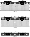
- Step 13.5 a back surface of an SOI substrate is thinned to remove a lower layer 420 and expose an intermediate insulating layer 410, as shown in a lower figure of FIG. 19 ; alternatively, a lower layer 420 of an SOI substrate is thinned and the lower layer 420 with a certain thickness is retained, as shown in an upper figure in FIG. 19 .
- step 11.5 the manner of thinning the wafer 100 may be similar to that in step 11.5, which will not be repeatedly described here.
- Step 13.6 dicing is performed along the insulating band 402 to obtain a packaged discrete device for each of the chip regions 110, as shown in FIG. 19 .
- the insulating band 402 since the insulating band 402 is thicker, after the wafer 100 is thinned, adjacent chip regions 110 are still connected by the insulating band 402, the insulating band 402 may be longitudinally cut by dicing technology to obtain the packaged discrete device of the chip region 110 as shown in FIG. 19 .
- a fourth embodiment of the chip packaging method 1000 will be described in detail below with reference to FIGS. 20 to 26 .
- the fourth embodiment includes the following steps (steps 14.1-14.6).
- Step 14.1 a region surrounding each of chip regions 110 on a scribe line 120 is converted into a porous silicon region by electrochemical etching or the like, and the porous silicon region forms an insulating band 501.
- a thickness of the insulating band 501 is greater than or equal to a thickness of the chip region 110 and less than or equal to a thickness of a wafer 100, and a width of the insulating band 501 is less than or equal to a width of the scribe line 120, where the insulating band 501 may be as shown in FIG. 20 .
- a portion of monocrystalline silicon on the scribe line 120 of the wafer 100 may be converted into porous silicon by electrochemical etching or other manners.
- the porous silicon is preferably mesoporous porous silicon with a pore diameter ranging from 2 to 50 nm.
- a side section of the insulating band 501 made of porous silicon may be any shape, for example, it may be arc-shaped as shown in FIG. 20 , but the embodiment of the present application is not limited thereto.
- a second protective layer 502 is first deposited on an upper surface of the wafer 100, for example, by means of plasma assisted deposition, a layer of fluoropolymer (fluoropolymer) is deposited on a front surface of the wafer 100 as the second protective layer 502; a second window that surrounds the chip region 110 is fabricated on a corresponding second protective layer above the scribe line 120, for example, a window is opened in the scribe line 202 region by photolithography; the wafer 100 is etched in a second chemical solution, to obtain the porous silicon region surrounding each of the chip regions 110 at the second window, that is, the insulating band 501; for example, the second chemical solution may be a mixed solution containing hydrofluoric acid, that is, the wafer 100 is placed in a solution containing hydrofluoric acid, to obtain the porous silicon layer as shown in FIG.
- fluoropolymer fluoropolymer
- FIG. 21 is a top view of the wafer 100, and a black region on an intermediate grid-shaped scribe lines 120 is the insulating band 501.
- a width of the insulating band 501 may refer to a maximum width on a side section of the insulating band 501; for example, as shown in FIG. 20 , the maximum width of the insulating band 501 is at an uppermost opening of the insulating band 501, that is, a diameter of a circle where the insulating band 501 is located, and the width is less than or equal to the width of the scribe line 120.
- Step 14.2 an insulating layer 503 is fabricated on an upper surface of a wafer 100, as shown in FIG. 22 .
- the insulating layer 503 may be formed by depositing an insulating material on the upper surface of the wafer 100.
- a process of depositing an insulating material on a surface of the wafer 100 may adopt the manner and material of depositing the insulating material as described in step 11.2, which will not be described repeatedly here.
- Step 14.3 a plurality of holes are fabricated on the insulating layer 503 above each of the plurality of chip regions 110 to expose each of the chip regions 110, for example, two holes are fabricated for each of the chip regions 110, as shown in FIG. 23 .
- step 14.3 is similar to step 11.3, which will not be repeatedly described here.
- Step 14.4 a conductive material is deposited in the plurality of holes to form a plurality of bonding pads 504; for example, as shown in FIG. 24 , two bonding pads 504 are correspondingly formed for each of the chip regions 110.
- step 14.4 is similar to step 11.4, which will not be repeatedly described here.
- Step 14.5 a back surface of the wafer 100 is thinned to expose the insulating band 501, as shown in FIG. 25 .
- step 11.5 the manner of thinning the wafer 100 may be similar to that in step 11.5, which will not be repeatedly described here.
- the wafer 100 may be thinned to expose a bottom portion of the insulating band 501, and the back surface of the wafer 100 is thinned to an effective thickness portion of a bottom layer of the chip region 110 to obtain the wafer 100 as shown in FIG. 25 .
- Step 14.6 dicing is performed along the insulating band 501 to obtain a packaged discrete device for each of the chip regions 110, as shown in FIG. 26 .
- the insulating band 501 since the insulating band 501 is thicker, after the back surface of the wafer 100 is thinned to the effective thickness portion of the bottom layer of the chip region 110, adjacent chip regions 110 are still connected by the insulating band 501, the insulating band 501 may be longitudinally cut by dicing technology to obtain the packaged discrete device of the chip region 110 as shown in FIG. 26 .
- the first embodiment of the chip packaging method 1000 in the Embodiment of the present application will be described in detail below with reference to a specific embodiment.
- Step 15.1 a wafer 100 obtained by processing a silicon wafer with a crystal orientation (100) is selected, where the wafer 100 includes a plurality of chip regions 110 and a grid-shaped scribe line 120.
- a top view of the wafer is shown in FIG. 2
- a cross-sectional view of the wafer is shown in FIG. 3 .
- a thickness of the chip region 110 is less than a thickness of the wafer 100.
- Step 15.2 as shown in FIG. 4 , a layer of silicon nitride 201 is deposited on an upper surface of the wafer 100 by plasma assisted deposition, and a window is opened in a region corresponding to the scribe line 120 by photolithography.
- the wafer 100 is etched in a potassium hydroxide solution to obtain an inverted trapezoidal trench 202 as shown in FIG. 4 .
- a maximum width of the trench 202 is less than a minimum width of the scribe line 120.
- a depth of the trench 202 ranges from tens to hundreds of microns, which is less than the thickness of the wafer 100 but greater than the thickness of the chip region 110.
- the silicon nitride 201 is removed.
- Step 15.3 by means of plasma enhanced chemical vapor deposition (plasma enhanced chemical vapor deposition, PECVD), a layer of USG with a thickness of 2 microns is deposited on a front surface of the wafer 100 and an inner wall of the trench 202 as the insulating layer 204 and the insulating band 203 respectively, as shown in FIG. 5 .
- PECVD plasma enhanced chemical vapor deposition
- two windows are opened in a region of the insulating layer 204 corresponding to the chip region 110 by photolithography, as shown in FIG. 6 .
- Step 15.4 a layer of aluminum with a thickness of 3 microns, a layer of nickel with a thickness of 200 nanometers, and a layer of gold with a thickness of 100 microns are deposited on the front surface of the wafer 100 by PVD, and a bonding pad 505 of the chip is patterned and fabricated by photolithography, as shown in FIG. 7 .
- Step 15.5 the wafer 100 is thinned to an effective thickness of the chip region 110 by mechanical grinding in combination with dry etching, as shown in FIG. 8 , to obtain discrete devices whose side walls are covered with an insulating material.
- the chip packaging method 1000 according to the embodiment of the present application is described in detail above with reference to FIGS. 1 to 26 , the bonding pads of the discrete device of the chip obtained by the method 1000 are located on the same side, and a chip packaging method 2000 according to another embodiment of the present application will be described below with reference to FIGS. 27 to 37 .
- FIG. 27 shows a schematic flowchart of a chip packaging method 2000 according to Embodiment 2 of the present application.
- the method 2000 includes: S2010, fabricating an insulating band on a scribe line of a wafer, where a front surface of the wafer is provided with a plurality of independent chip regions, a portion between any two adjacent chip regions of the plurality of chip regions is the scribe line, and between the any two adjacent chip regions, a depth of the insulating band is greater than or equal to a thickness of the chip region and less than or equal to a thickness of the wafer, and a width of the insulating band is less than or equal to a width of the scribe line; S2020, fabricating a first insulating layer on an upper surface of the wafer; S2030, fabricating at least one first window on the first insulating layer above each of a plurality of chip regions to expose each of the chip regions; S2040, depositing a conductive material in the at least one first window to form at
- the wafer in the method 2000 may be the same as the wafer 100 in the method 1000, as shown in FIGS. 2 and 3 , which will not be repeatedly described here.
- the manner of forming the first bonding pad may refer to the foregoing methods in the first to fourth embodiments, certainly, the number and size of the corresponding holes formed in the chip region may also be varied according to requirements of the number and size of the bonding pads.
- the insulating band is fabricated on the scribe line 120 of the wafer 100.
- the insulating band may be fabricated in various ways, and the chip may be packaged according to different insulating bands.
- fabricating the insulating band may include fabricating a trench on the scribe line 120 and depositing an insulating material in the trench to form the insulating band; or by electrochemical etching or other manners, converting a portion of a region of the scribe line 120 into a porous silicon region or an insulating region made of other materials as an insulating band.
- the depositing the conductive material on the back surface of the thinned wafer to form the second bonding pad for each of the chip regions may include: depositing an insulating material on the back surface of the thinned wafer to form a second insulating layer; fabricating, on the second insulating layer below each of the chip regions, at least one second window to expose each of the chip regions; and depositing a conductive material in the at least one second window to form the at least one second bonding pad of each of the chips.
- the first embodiment of chip packaging method 2000 will be described in detail with reference to FIGS. 28 to 32 .
- the first embodiment of the method 2000 includes the following steps (steps 21.1-21.7).
- Step 21.1 is the same as step 12.1, which will not be repeatedly described here.
- Step 21.2 is the same as step 12.2, which will not be repeatedly described here.
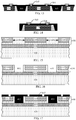
- Step 21.3 at least one first window is formed on an insulating layer 304 above each of chip regions 100 to expose each of the chip regions 110; for example, one first window is correspondingly fabricated for each of the chip regions 110, as shown in FIG. 28 .
- a size of the first window on the insulating layer 304 is not limited here.
- the first window may be larger.
- a process of fabricating any one of first windows on the insulating layer 304 may be the same as a process of fabricating any one of a plurality of holes in step 12.3, which will not be repeatedly described here.
- Step 21.4 a conductive material is deposited in the at least one first window to form at least one first bonding pad 310 of each of the chip regions; for example, as shown in FIG. 29 , each of the chip regions corresponding to one first bonding pad 310 is taken as an example.
- a process of depositing the conductive material to form any one of the first bonding pads 310 may be the same as a process of fabricating any one of the bonding pads in step 11.4, which will not be repeatedly described here.
- the number of the at least one first window is greater than or equal to the number of the at least one first bonding pad 310, that is, there may be a case where two or more first windows form one first bonding pad 310 correspondingly.
- Step 21.5 a back surface of a wafer 100 is thinned to expose an insulating band 303, as shown in FIG. 30 .
- step 21.5 is the same as step 12.5, which will not be repeatedly described here.
- Step 21.6 a conductive material is deposited on a back surface of a thinned wafer 100 to form a second bonding pad 320 for each of the chip regions, as shown in FIG. 31 .
- a process of fabricating the second bonding pad 320 on the back surface of the thinned wafer 100 is the same as that of the first bonding pad 310, that is, an insulating material is deposited on the thinned wafer 100 to form a second insulating layer 308; at least one second window is fabricated on the second insulating layer 308 below each of the chip regions 110 to expose each of the chip regions 110; and a conductive material is deposited in the at least one second window to form at least one second bonding pad 320 for each of the chip regions.
- fabricating a second window under each of the chip regions 110 to form a second bonding pad 320 is taken as an example.
- Step 21.7 dicing is performed along the insulating band 303 to obtain the packaged discrete device for each of the chip regions 110, as shown in FIGS. 31 and 32 .
- step 21.7 is the same as step 12.6, which will not be repeatedly described here.
- a second embodiment of the chip packaging method 2000 will be described in detail with reference to FIGS. 33 to 37 .
- the second embodiment of the method 2000 includes the following steps (steps 22.1-22.7).
- Step 22.1 is the same as step 14.1, which will not be repeatedly described here.
- Step 22.2 is the same as step 14.2, which will not be repeatedly described here.
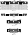
- Step 22.3 at least one first window is fabricated on an insulating layer 503 above each of plurality of chip regions 11 to expose each of the chip regions 110; for example, one first window is correspondingly fabricated for each chip region 110, as shown in FIG. 33 .
- a size of the first window on the insulating layer 503 is not limited here.
- the first window may be larger.
- a process of fabricating any one of first windows on the insulating layer 503 may be the same as a process of fabricating any one of a plurality of holes in step 14.3, which will not be repeatedly described here.
- Step 22.4 a conductive material is deposited in the at least one first window to form at least one first bonding pad 510 of each of the chip regions; for example, as shown in FIG. 34 , each of the chip regions corresponding to one first bonding pad 510 is taken as an example.
- a process of depositing the conductive material to form any one of the first bonding pads 51 may be the same as a process of fabricating any one of the bonding pads in step 11.4, which will not be repeatedly described here.
- the number of the at least one first window is greater than or equal to the number of the at least one first bonding pad 510, that is, there may be a case where two or more first windows form one first bonding pad 510 correspondingly.
- Step 22.5 a back surface of a wafer 100 is thinned to expose an insulating band 501, as shown in FIG. 35 .
- step 22.5 is the same as step 14.5, which will not be repeatedly described here.
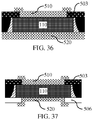
- Step 22.6 a conductive material is deposited on a back surface of a thinned wafer 100 to form a second bonding pad 520 for each of the chip regions, as shown in FIG. 36 .
- a process of fabricating the second bonding pad 520 on the back surface of the thinned wafer 100 is the same as that of the first bonding pad 510, that is, an insulating material is deposited on the thinned wafer 100 to form a second insulating layer 506; at least one second window is fabricated on the second insulating layer 506 below each of the chip regions 110 to expose each of the chip regions 110; and a conductive material is deposited in the at least one second window to form at least one second bonding pad 520 for each of the chip regions.
- fabricating a second window under each of the chip regions 110 to form a second bonding pad 520 is taken as an example.
- Step 22.7 dicing is performed along the insulating band 501 to obtain the packaged discrete device for each of the chip regions 110, as shown in FIGS. 36 and 37 .
- step 21.7 is the same as step 14.6, which will not be repeatedly described here.
- a second embodiment of the chip packaging method 2000 in the Embodiment of the present application will be described in detail below with reference to a specific embodiment.
- Step 23.1 a wafer 100 obtained by processing a P-type heavily doped silicon wafer is selected, where the wafer 100 includes a plurality of chip regions 110 and a grid-shaped scribe line 120.
- a thickness of the chip region 110 is less than a thickness of the wafer 100, as shown in FIGS. 2 and 3 .
- Step 23.2 as shown in FIG. 20 , a layer of fluoropolymer (fluoropolymer) 502 is deposited on a front surface of the wafer 100 by plasma assisted deposition, and a window is opened in a region corresponding to the scribe line 120 by photolithography.
- the wafer 100 is etched in a solution containing hydrofluoric acid by electrochemical etching to obtain a porous silicon layer 501 as shown in FIG. 20 .
- a maximum width of the porous silicon layer 501 is less than a minimum width of the scribe line 120.
- a depth of the porous silicon layer 501 ranges from tens to hundreds of microns, which is less than the thickness of the wafer 100 but greater than the thickness of the chip region 120.
- the fluoropolymer 502 is removed to obtain a top view of the wafer as shown in FIG. 21 .
- Step 23.3 by means of PECVD, a layer of USG with a thickness of 2 microns is deposited on the front surface of the wafer 100 as an insulating layer 503, as shown in FIG. 22 .
- a window is opened in the insulating layer 503 above the chip region 110 by photolithography, as shown in FIG. 33 .
- Step 23.4 a layer of aluminum with a thickness of 3 microns, a layer of nickel with a thickness of 200 nanometers, and a layer of gold with a thickness of 100 microns are deposited on the front surface of the wafer by PVD, and a bonding pad 510 of the chip is patterned and fabricated by photolithography, as shown in FIG. 34 .
- Step 23.5 the wafer is thinned to an effective thickness of the chip region 110 by mechanical grinding and polishing, as shown in FIG. 35 .
- Steps 23.6 and 23.7 steps 23.3 and 23.4 are repeated, that is, an insulating layer 506 and a back bonding pad 520 are fabricated on a back surface of a thinned wafer 100, as shown in FIG. 37 .
- Step 23.8 dicing is performed along the scribe line to obtain discrete devices whose side walls are made of porous silicon, as shown in FIG. 37 .
- a semiconductor device with side protection is fabricated, including a passive device (a capacitor, an inductor, a resistor, and the like), an energy storage device, or the like.
- an insulation protection method for a side surface of a wafer-level chip in a semiconductor front-end process is achieved by fabricating a trench surrounding chips and having an insulating material therein, or by fabricating a grid-shaped porous silicon region surrounding chips, so that a step of packaging a single chip at a back end is omitted, cost is lower, and a chip volume is smaller, thereby resolving a contradiction of insulation protection for a side surface of a semiconductor discrete device and complicated packaging procedures at the back end.
- B corresponding to A indicates that B is associated with A, and B may be determined based on A.
- determining B based on A does not mean that B is determined based on A only; and B may also be determined based on A and/or other information.
- sequence numbers of the foregoing processes do not mean execution sequences in various embodiments of this application.
- the execution sequences of the processes should be determined according to functions and internal logic of the processes, and should not be construed as any limitation on the implementation processes of the embodiments of this application.
Landscapes
- Dicing (AREA)
- Engineering & Computer Science (AREA)
- Manufacturing & Machinery (AREA)
- Internal Circuitry In Semiconductor Integrated Circuit Devices (AREA)
Applications Claiming Priority (1)
| Application Number | Priority Date | Filing Date | Title |
|---|---|---|---|
| PCT/CN2018/098583 WO2020024277A1 (fr) | 2018-08-03 | 2018-08-03 | Procédé d'encapsulation de puce |
Publications (1)
| Publication Number | Publication Date |
|---|---|
| EP3624177A1 true EP3624177A1 (fr) | 2020-03-18 |
Family
ID=64806251
Family Applications (1)
| Application Number | Title | Priority Date | Filing Date |
|---|---|---|---|
| EP18914930.5A Withdrawn EP3624177A1 (fr) | 2018-08-03 | 2018-08-03 | Procédé d'encapsulation de puce |
Country Status (4)
| Country | Link |
|---|---|
| US (1) | US20200058518A1 (fr) |
| EP (1) | EP3624177A1 (fr) |
| CN (1) | CN109155281A (fr) |
| WO (1) | WO2020024277A1 (fr) |
Families Citing this family (8)
| Publication number | Priority date | Publication date | Assignee | Title |
|---|---|---|---|---|
| KR102619666B1 (ko) | 2016-11-23 | 2023-12-29 | 삼성전자주식회사 | 이미지 센서 패키지 |
| CN112151368B (zh) * | 2019-06-28 | 2025-05-30 | 长鑫存储技术有限公司 | 晶圆及其制作方法、半导体器件 |
| DE102019120844A1 (de) * | 2019-08-01 | 2021-02-04 | Horst Siedle Gmbh & Co. Kg | Verfahren zur Herstellung von abgedichteten Funktionselementen |
| CN113363135A (zh) * | 2021-05-14 | 2021-09-07 | 深圳市嘉也科技有限公司 | 一种用于芯片的镀膜加工方法 |
| CN114295960A (zh) * | 2021-12-29 | 2022-04-08 | 南京宙讯微电子科技有限公司 | Saw滤波器及双工器、芯片的晶圆测试结构及芯片制造方法 |
| CN114669452B (zh) * | 2022-03-26 | 2023-06-06 | 宁波芯健半导体有限公司 | 一种超薄芯片背胶涂覆方法、涂覆装置及存储介质 |
| CN116207182B (zh) * | 2023-01-29 | 2024-03-12 | 北京智创芯源科技有限公司 | 芯片制备方法及电子器件 |
| JP2025030810A (ja) * | 2023-08-24 | 2025-03-07 | 国立大学法人 東京大学 | 化合物半導体チップ |
Family Cites Families (16)
| Publication number | Priority date | Publication date | Assignee | Title |
|---|---|---|---|---|
| US5904496A (en) * | 1997-01-24 | 1999-05-18 | Chipscale, Inc. | Wafer fabrication of inside-wrapped contacts for electronic devices |
| JP5082211B2 (ja) * | 2005-03-25 | 2012-11-28 | 富士電機株式会社 | 半導体装置の製造方法 |
| CN101064261A (zh) * | 2006-04-25 | 2007-10-31 | 矽品精密工业股份有限公司 | 半导体封装件及其呈阵列排列的基片结构与制法 |
| US20100207227A1 (en) * | 2009-02-16 | 2010-08-19 | Georg Meyer-Berg | Electronic Device and Method of Manufacturing Same |
| CN102097287B (zh) * | 2009-12-15 | 2012-07-25 | 北大方正集团有限公司 | 一种监控芯片沟槽深度的方法及晶圆 |
| CN101789414B (zh) * | 2010-02-26 | 2011-08-17 | 苏州晶方半导体科技股份有限公司 | 超薄半导体芯片封装结构及其制造工艺 |
| CN102593085B (zh) * | 2011-01-10 | 2014-08-13 | 原相科技股份有限公司 | 芯片封装结构以及芯片封装制程 |
| CN102774805B (zh) * | 2011-05-13 | 2015-10-28 | 精材科技股份有限公司 | 晶片封装体及其形成方法 |
| US8563361B2 (en) * | 2012-02-14 | 2013-10-22 | Alpha & Omega Semiconductor, Inc. | Packaging method of molded wafer level chip scale package (WLCSP) |
| US9196532B2 (en) * | 2012-06-21 | 2015-11-24 | Taiwan Semiconductor Manufacturing Company, Ltd. | Integrated circuit packages and methods for forming the same |
| US9337154B2 (en) * | 2014-08-28 | 2016-05-10 | Taiwan Semiconductor Manufacturing Company Ltd. | Semiconductor device and method of manufacturing the same |
| TWI560758B (en) * | 2014-10-20 | 2016-12-01 | Niko Semiconductor Co Ltd | Manufacturing method of wafer level chip scale package structure |
| CN105590867A (zh) * | 2014-10-24 | 2016-05-18 | 无锡超钰微电子有限公司 | 晶圆级芯片尺寸封装结构的制造方法 |
| CN105070665A (zh) * | 2015-07-16 | 2015-11-18 | 北京工业大学 | 一种晶圆级薄片封装工艺 |
| CN105938804A (zh) * | 2016-06-28 | 2016-09-14 | 中芯长电半导体(江阴)有限公司 | 一种晶圆级芯片封装方法及封装件 |
| CN207557977U (zh) * | 2017-12-05 | 2018-06-29 | 深圳市为通博科技有限责任公司 | 光路调制器、指纹识别装置和终端设备 |
-
2018
- 2018-08-03 WO PCT/CN2018/098583 patent/WO2020024277A1/fr not_active Ceased
- 2018-08-03 CN CN201880001019.4A patent/CN109155281A/zh active Pending
- 2018-08-03 EP EP18914930.5A patent/EP3624177A1/fr not_active Withdrawn
-
2019
- 2019-10-27 US US16/664,892 patent/US20200058518A1/en not_active Abandoned
Also Published As
| Publication number | Publication date |
|---|---|
| CN109155281A (zh) | 2019-01-04 |
| WO2020024277A1 (fr) | 2020-02-06 |
| US20200058518A1 (en) | 2020-02-20 |
Similar Documents
| Publication | Publication Date | Title |
|---|---|---|
| EP3624177A1 (fr) | Procédé d'encapsulation de puce | |
| US12224297B2 (en) | Method of forming an image sensor having stress releasing structure | |
| TWI588950B (zh) | 封裝半導體裝置以及形成封裝半導體裝置之方法 | |
| US7906431B2 (en) | Semiconductor device fabrication method | |
| CN104779243B (zh) | 3dic密封环结构及其形成方法 | |
| CN110943052B (zh) | 晶片封装体及其制造方法 | |
| CN102598245B (zh) | 同轴硅通孔 | |
| US11694979B2 (en) | Isolation structure for bond pad structure | |
| US10818612B2 (en) | Manufacturing method of semiconductor structure | |
| CN106611761B (zh) | 使用前侧深沟槽刻蚀隔离电路元件 | |
| US20150348874A1 (en) | 3DIC Interconnect Devices and Methods of Forming Same | |
| TWI869452B (zh) | 半導體結構的製作方法 | |
| US11908838B2 (en) | Three-dimensional device structure including embedded integrated passive device and methods of making the same | |
| US20100078776A1 (en) | On-Chip RF Shields with Backside Redistribution Lines | |
| CN103107157B (zh) | 晶片封装体及其形成方法 | |
| CN102774805B (zh) | 晶片封装体及其形成方法 | |
| US12442995B2 (en) | Photonic integrated circuit and package structure | |
| US20240347578A1 (en) | Manufacturing method of semiconductor device with inductor | |
| CN110391145A (zh) | 半导体器件及其形成方法 | |
| US10056427B1 (en) | Front side illuminated image sensor device structure and method for forming the same | |
| CN221994468U (zh) | 半导体管芯封装 | |
| CN102779809B (zh) | 晶片封装体及其形成方法 | |
| US9887134B2 (en) | Semiconductor devices, methods of manufacture thereof, and methods of singulating semiconductor devices | |
| US20250300154A1 (en) | Semiconductor package and manufacturing method thereof |
Legal Events
| Date | Code | Title | Description |
|---|---|---|---|
| PUAI | Public reference made under article 153(3) epc to a published international application that has entered the european phase |
Free format text: ORIGINAL CODE: 0009012 |
|
| 17P | Request for examination filed |
Effective date: 20191023 |
|
| AK | Designated contracting states |
Kind code of ref document: A1 Designated state(s): AL AT BE BG CH CY CZ DE DK EE ES FI FR GB GR HR HU IE IS IT LI LT LU LV MC MK MT NL NO PL PT RO RS SE SI SK SM TR |
|
| AX | Request for extension of the european patent |
Extension state: BA ME |
|
| RIN1 | Information on inventor provided before grant (corrected) |
Inventor name: SHEN, JIAN Inventor name: LU, BIN |
|
| RIC1 | Information provided on ipc code assigned before grant |
Ipc: H01L 21/56 20060101ALI20200529BHEP Ipc: H01L 21/78 20060101AFI20200529BHEP |
|
| STAA | Information on the status of an ep patent application or granted ep patent |
Free format text: STATUS: THE APPLICATION HAS BEEN WITHDRAWN |
|
| 18W | Application withdrawn |
Effective date: 20200713 |