WO2020024277A1 - Procédé d'encapsulation de puce - Google Patents
Procédé d'encapsulation de puce Download PDFInfo
- Publication number
- WO2020024277A1 WO2020024277A1 PCT/CN2018/098583 CN2018098583W WO2020024277A1 WO 2020024277 A1 WO2020024277 A1 WO 2020024277A1 CN 2018098583 W CN2018098583 W CN 2018098583W WO 2020024277 A1 WO2020024277 A1 WO 2020024277A1
- Authority
- WO
- WIPO (PCT)
- Prior art keywords
- wafer
- chip
- insulating
- depositing
- region
- Prior art date
- Legal status (The legal status is an assumption and is not a legal conclusion. Google has not performed a legal analysis and makes no representation as to the accuracy of the status listed.)
- Ceased
Links
Images







Classifications
-
- H—ELECTRICITY
- H10—SEMICONDUCTOR DEVICES; ELECTRIC SOLID-STATE DEVICES NOT OTHERWISE PROVIDED FOR
- H10W—GENERIC PACKAGES, INTERCONNECTIONS, CONNECTORS OR OTHER CONSTRUCTIONAL DETAILS OF DEVICES COVERED BY CLASS H10
- H10W74/00—Encapsulations, e.g. protective coatings
- H10W74/01—Manufacture or treatment
- H10W74/014—Manufacture or treatment using batch processing
-
- H—ELECTRICITY
- H10—SEMICONDUCTOR DEVICES; ELECTRIC SOLID-STATE DEVICES NOT OTHERWISE PROVIDED FOR
- H10P—GENERIC PROCESSES OR APPARATUS FOR THE MANUFACTURE OR TREATMENT OF DEVICES COVERED BY CLASS H10
- H10P54/00—Cutting or separating of wafers, substrates or parts of devices
-
- H—ELECTRICITY
- H10—SEMICONDUCTOR DEVICES; ELECTRIC SOLID-STATE DEVICES NOT OTHERWISE PROVIDED FOR
- H10W—GENERIC PACKAGES, INTERCONNECTIONS, CONNECTORS OR OTHER CONSTRUCTIONAL DETAILS OF DEVICES COVERED BY CLASS H10
- H10W72/00—Interconnections or connectors in packages
- H10W72/01—Manufacture or treatment
- H10W72/019—Manufacture or treatment of bond pads
-
- H—ELECTRICITY
- H10—SEMICONDUCTOR DEVICES; ELECTRIC SOLID-STATE DEVICES NOT OTHERWISE PROVIDED FOR
- H10W—GENERIC PACKAGES, INTERCONNECTIONS, CONNECTORS OR OTHER CONSTRUCTIONAL DETAILS OF DEVICES COVERED BY CLASS H10
- H10W72/00—Interconnections or connectors in packages
- H10W72/01—Manufacture or treatment
- H10W72/0198—Manufacture or treatment batch processes
-
- H—ELECTRICITY
- H10—SEMICONDUCTOR DEVICES; ELECTRIC SOLID-STATE DEVICES NOT OTHERWISE PROVIDED FOR
- H10W—GENERIC PACKAGES, INTERCONNECTIONS, CONNECTORS OR OTHER CONSTRUCTIONAL DETAILS OF DEVICES COVERED BY CLASS H10
- H10W72/00—Interconnections or connectors in packages
- H10W72/90—Bond pads, in general
-
- H—ELECTRICITY
- H10—SEMICONDUCTOR DEVICES; ELECTRIC SOLID-STATE DEVICES NOT OTHERWISE PROVIDED FOR
- H10W—GENERIC PACKAGES, INTERCONNECTIONS, CONNECTORS OR OTHER CONSTRUCTIONAL DETAILS OF DEVICES COVERED BY CLASS H10
- H10W74/00—Encapsulations, e.g. protective coatings
- H10W74/10—Encapsulations, e.g. protective coatings characterised by their shape or disposition
- H10W74/111—Encapsulations, e.g. protective coatings characterised by their shape or disposition the semiconductor body being completely enclosed
- H10W74/129—Encapsulations, e.g. protective coatings characterised by their shape or disposition the semiconductor body being completely enclosed forming a chip-scale package [CSP]
-
- H—ELECTRICITY
- H10—SEMICONDUCTOR DEVICES; ELECTRIC SOLID-STATE DEVICES NOT OTHERWISE PROVIDED FOR
- H10W—GENERIC PACKAGES, INTERCONNECTIONS, CONNECTORS OR OTHER CONSTRUCTIONAL DETAILS OF DEVICES COVERED BY CLASS H10
- H10W72/00—Interconnections or connectors in packages
- H10W72/90—Bond pads, in general
- H10W72/941—Dispositions of bond pads
- H10W72/944—Dispositions of multiple bond pads
Definitions
- the present application relates to the field of chips, and in particular, to a method for chip packaging.
- packaging mainly plays a role of leading out the pins of the chip and isolating the chip from the outside world.
- back-end packaging mainly plays a role of leading out the pins of the chip and isolating the chip from the outside world.
- WLCSP wafer-level chip-scale packaging
- SMD surface-mounted devices
- eWLCSP Encapsulated WLCSP
- Another technique is to use an injection mold to cover the front side of the wafer manufactured in the front and the pre-formed dicing groove with plastic sealing material, and then combine the Redistribution Layer (RDL) process to reduce the back side of the wafer.
- RDL Redistribution Layer
- This application provides a method for chip packaging, which can use the semiconductor front-end process to perform wafer-side chip side insulation protection, eliminating the need for subsequent packaging steps for a single chip, lower cost, and smaller chip size.
- a chip packaging method includes: manufacturing an insulating tape on a dicing path of a wafer, wherein a plurality of independent chip regions are provided on the front surface of the wafer, and any two of the plurality of chip regions The portion between two adjacent chip areas is a dicing track. Between the two adjacent chip areas, the depth of the insulating tape is greater than or equal to the thickness of the chip area and less than or equal to that of the wafer. Thickness, the width of the insulating tape is less than or equal to the width of the dicing track; an insulating layer is made on the upper surface of the wafer; and more is made on the insulating layer above each of the plurality of chip regions. Holes to expose each of the chip areas; depositing a conductive material in the plurality of holes to form a plurality of pads; thinning the back of the wafer to obtain discrete parts of each chip area after packaging Device.
- the making an insulating tape on a dicing track of a wafer includes: making a groove on the dicing track that surrounds each chip region; and An insulating material is deposited on the inner surface of the trench, the trench after depositing the insulating material forms the insulating tape, and the depth of the trench after depositing the insulating material is greater than or equal to the thickness of each chip region; the thinning The back surface of the wafer to obtain discrete devices for each chip region after packaging includes: thinning the back surface of the wafer to separate the multiple chip regions to obtain each chip after packaging. Discrete devices.
- the manufacturing an insulating tape on a dicing path of a wafer includes: manufacturing, on the dicing path, an area surrounding each chip area. A trench, the depth of which is greater than or equal to the thickness of the surrounding chip region and less than or equal to the thickness of the wafer; depositing an insulating material inside the trench to form the insulating tape; Said back side of the wafer to obtain the discrete devices of each chip region after packaging includes: thinning the back side of the wafer to expose the insulating tape, and dicing along the insulating tape to obtain the post-packaged A discrete device for each chip region.
- the step of making grooves surrounding the each chip region on the dicing path includes: dry etching, wet At least one of etching and mechanical cutting is used to form the groove on the cutting track.
- the at least one of dry etching, wet etching, and mechanical cutting is performed on the cutting lane.
- the trench includes: depositing a first protective layer on an upper surface of the wafer; making a first window on the first protective layer above the dicing track; and placing the wafer in a first chemical solution Etch to obtain the trench at the first window.
- the depositing a first protective layer on the upper surface of the wafer includes: A silicon nitride layer is deposited on the upper surface of the wafer as the first protective layer, and the first chemical solution is any one of the following solutions: potassium hydroxide solution, sodium hydroxide (NaOH) solution, tetramethyl hydroxide Ammonium (TMAH) solution and HNA, a mixed solution containing hydrofluoric acid and nitric acid.
- potassium hydroxide solution sodium hydroxide (NaOH) solution
- TMAH tetramethyl hydroxide Ammonium
- HNA a mixed solution containing hydrofluoric acid and nitric acid.
- the groove is a trapezoid having a bottom width smaller than an upper width; or the groove is a rectangle having a bottom width equal to the upper width.
- the manufacturing an insulating tape on a dicing path of a wafer includes: by electrochemical etching, surrounding the dicing path with each of the dicing paths. A part of each chip region is converted into a porous silicon region, and the porous silicon region is the insulating tape; and the thinning of the backside of the wafer to obtain the packaged discrete devices of each chip region includes: Thin the backside of the wafer to expose the insulating tape, and scribe along the insulating tape to obtain discrete devices of each chip region after packaging.
- the part of the scribe line surrounding the each chip region on the dicing track is converted into a porous silicon region by electrochemical etching, including: : Depositing a second protective layer on the upper surface of the wafer; making a second window on the second protective layer above the dicing track; placing the wafer in a second chemical solution and passing the electricity By chemical etching, the porous silicon region is obtained at the second window.
- the depositing a second protective layer on the upper surface of the wafer includes: A fluorine-containing polymer layer deposited on the upper surface of the wafer is the second protective layer, and the second chemical solution is a mixed solution containing hydrofluoric acid.
- the wafer includes an insulating layer, the insulating layer is disposed below each of the chip regions, and the insulating tape and the Said insulation layer connection.
- the thinning the back surface of the wafer to obtain discrete components of each chip region after packaging includes: Thin the backside of the wafer to expose the insulating layer and scribe along the insulating tape to obtain discrete devices for each of the chip regions after packaging.
- the thinning the back surface of the wafer includes: grinding, grinding, chemical mechanical polishing, dry polishing, electrochemical At least one of etching, wet etching, plasma-assisted chemical etching, and atmospheric pressure plasma etching is used to thin the back surface of the wafer.
- the manufacturing an insulating layer on the upper surface of the wafer includes: depositing an insulating material on the upper surface of the wafer to form The insulation layer.
- the depositing of the insulating material includes: at least one of physical vapor deposition, chemical vapor deposition, plasma-assisted deposition, spray coating, and spin coating. In one way, the insulating material is deposited.
- the insulating material includes at least one of the following: an oxide of silicon, a nitride of silicon, and a polymer.
- the depositing the conductive material includes: through atomic layer deposition, physical vapor deposition, organometallic chemical vapor deposition, evaporation, and electroplating. At least one way, the conductive material is deposited.
- the conductive material includes at least one of the following: heavily doped polysilicon, a carbon-based material, a metal, and titanium nitride.
- a chip packaging method includes: manufacturing an insulating tape on a dicing path of a wafer, wherein a plurality of independent chip regions are provided on the front surface of the wafer, and any two of the plurality of chip regions are provided.
- the portion between two adjacent chip areas is a dicing track. Between the two adjacent chip areas, the depth of the insulating tape is greater than or equal to the thickness of the chip area and less than or equal to that of the wafer.
- the width of the insulating tape is less than or equal to the width of the scribe line; making a first insulating layer on the upper surface of the wafer; the first insulation above each of the plurality of chip regions A first window is made on the layer to expose each of the chip regions; a conductive material is deposited in the first window to form a first pad of each chip; and the back of the wafer is thinned to expose The insulating tape; depositing a conductive material on the back of the thinned wafer to form a second pad of each chip region, and dicing along the insulating tape to obtain the Discrete devices in each chip area.
- the depositing a conductive material on the back surface of the wafer after thinning to form the second pad of each chip region includes: An insulating material is deposited on the back of the thin wafer to form a second insulating layer; a second window is formed on the second insulating layer below each chip region to expose each chip region; A conductive material is deposited in the second window to form the second pad of each chip.
- the first insulating layer and the second insulating layer are made of the same material.
- the manufacturing an insulating tape on a dicing path of a wafer includes: manufacturing, on the dicing path, surrounding each chip region. A trench whose depth is greater than or equal to the thickness of the surrounding chip region and less than or equal to the thickness of the wafer; an insulating material is deposited inside the trench to form the insulating tape.
- the step of making grooves around the each chip region on the dicing path includes: dry etching, wet At least one of etching and mechanical cutting is used to form the groove on the cutting track.
- the at least one of dry etching, wet etching, and mechanical cutting is performed on the cutting lane.
- the trench includes: depositing a first protective layer on an upper surface of the wafer; making a third window on the first protective layer above the dicing track; placing the wafer in a first chemical solution Etching, at the third window, the trench is obtained.
- the depositing the first protective layer on the upper surface of the wafer includes:
- the silicon nitride layer deposited on the upper surface of the wafer is the first protective layer
- the first chemical solution is any one of the following solutions: potassium hydroxide solution, sodium hydroxide (NaOH) solution, tetramethyl hydroxide Ammonium (TMAH) solution and HNA, a mixed solution containing hydrofluoric acid and nitric acid.
- the groove is a trapezoid having a bottom width smaller than the upper width; or the groove is a rectangle with a bottom width equal to the upper width.
- the manufacturing an insulating tape on a dicing path of a wafer includes: by electrochemical etching, wrapping the dicing path around the each A part of each chip region is converted into a porous silicon region, and the porous silicon region is the insulating tape.
- the part of the scribe line surrounding the each chip region on the dicing track is converted into a porous silicon region by electrochemical etching, including: : Depositing a second protective layer on the upper surface of the wafer; making a fourth window on the second protective layer above the dicing track; placing the wafer in a second chemical solution and passing the electricity By chemical etching, the porous silicon region is obtained at the fourth window.
- the depositing a second protective layer on the upper surface of the wafer includes: A fluorine-containing polymer layer deposited on the upper surface of the wafer is the second protective layer, and the second chemical solution is a mixed solution containing hydrofluoric acid.
- the first pad is the same as the second pad material.
- the thinning the back surface of the wafer includes: grinding, grinding, chemical mechanical polishing, dry polishing, electrochemical At least one of etching, wet etching, plasma-assisted chemical etching, and atmospheric pressure plasma etching is used to thin the back surface of the wafer.
- the manufacturing an insulating layer on the upper surface of the wafer includes: depositing an insulating material on the upper surface of the wafer to form The insulation layer.
- the depositing the insulating material includes: depositing by at least one of physical vapor deposition, chemical vapor deposition, spray coating, and spin coating, The insulating material.
- the insulating material includes at least one of the following: an oxide of silicon, a nitride of silicon, and a polymer.
- the depositing the conductive material includes: through atomic layer deposition, physical vapor deposition, organometallic chemical vapor deposition, evaporation, and electroplating. At least one way, the conductive material is deposited.
- the conductive material includes at least one of the following: heavily doped polysilicon, a carbon-based material, a metal, and titanium nitride.
- the insulating tape is in a grid shape as a whole; wherein the dicing track is in a grid shape on the wafer as a whole, and the chip area is between the grids, which can be formed at the corresponding position of the grid-like grid dicing track. Corresponding grid-like insulation tape.
- crystals are formed in the semiconductor front-end process by making grooves surrounding the chip with insulating material inside, or by making grid-shaped porous silicon regions around the chip.
- the method of side-level insulation and protection of a round chip eliminates the need for subsequent packaging steps for a single chip, lower cost, and smaller chip size, thereby solving the contradictory contradiction of side-side insulation protection of semiconductor discrete devices and subsequent packaging processes.
- FIG. 1 is a schematic flowchart of a chip packaging method according to Embodiment 1 of the present application.
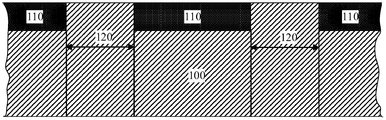
- FIG. 2 is a top view of a wafer according to an embodiment of the present application.
- FIG. 3 is a cross-sectional view of a wafer according to an embodiment of the present application.
- FIG. 4 to FIG. 8 are schematic diagrams of the structure of a wafer and a chip in each step of the chip packaging according to the first embodiment of the chip packaging method according to the first embodiment of the present application;
- FIG. 9 to FIG. 14 are schematic structural diagrams of a wafer and a chip in each step of chip packaging according to the second embodiment of the chip packaging method according to Embodiment 1 of the present application;
- 15-19 are schematic diagrams of the structure of a wafer and a chip in each step of chip packaging according to the third embodiment of the chip packaging method according to the first embodiment of the present application;
- 20 to 26 are schematic diagrams of a structure of a wafer and a chip in each step of the chip packaging according to the fourth embodiment of the chip packaging method according to Embodiment 1 of the present application;
- FIG. 27 is a schematic flowchart of a chip packaging method according to Embodiment 2 of the present application.
- 28 to 31 are schematic diagrams of the structure of a wafer and a chip in each step of the chip packaging according to the first embodiment of the chip packaging method according to the second embodiment of the present application.
- 32 to 37 are schematic diagrams of the structure of a wafer and a chip in each step of the chip packaging according to the second embodiment of the chip packaging method according to the first embodiment of the present application.
- FIG. 1 shows a schematic flowchart of a chip packaging method 1000 according to an embodiment of the present application.
- the method 1000 includes: S1010, manufacturing an insulating tape on a scribe line of a wafer, wherein the wafer There are a plurality of independent chip regions on the front surface, and a portion between any two adjacent chip regions of the plurality of chip regions is a scribe line.
- the depth of the insulating tape is greater than or equal to The thickness of the chip area is less than or equal to the thickness of the wafer, and the width of the insulating tape is less than or equal to the width of the scribe line;
- S1020 an insulating layer is formed on the upper surface of the wafer;
- S1030 in the plurality of chip areas A plurality of holes are made on the insulating layer above each chip area to expose each chip area;
- S1040 a conductive material is deposited in the plurality of holes to form a plurality of pads;
- S1050 the back of the wafer is thinned, To obtain discrete devices for each chip region after packaging.
- the wafer in the embodiment of the present application may be the wafer 100 shown in FIG. 2 and FIG. 3.
- FIG. 2 shows a top view of the wafer 100 according to the embodiment of the present application
- the wafer 100 includes a plurality of independent chip regions 110, and the plurality of chip regions 110 may be uniformly arranged as shown in FIG. 2, that is, a horizontal level between two adjacent chip regions 110 in a horizontal direction. The distance is the same, the vertical distance between two adjacent chip areas 110 in the vertical direction is also the same, and the horizontal distance and the vertical distance are also the same.
- the chip areas 110 on the wafer 100 may be uneven.
- the arrangement for example, is different between horizontal distances, or between vertical distances, or between horizontal and vertical distances, and embodiments of the present application are not limited thereto.
- each chip region 110 on the wafer 100 is smaller than the thickness of the wafer 100.
- the thickness of each chip region 110 can be set according to the thickness of the chip to be packaged or the type of the chip to be packaged.
- the thickness of the chip region 110 referred to in the embodiment of the present application refers to the effective thickness of the chip region 100 in practical applications.
- the area on the wafer 100 other than the chip area 110 is a scribe line 120, that is, the scribe line 120 is an area between two adjacent chip areas 110. As shown in FIG. 2, the scribe line 120 is in a grid shape. Correspondingly, the insulating tape made on the scribe line 120 of the wafer 100 is also grid-shaped.
- an insulating tape is made on the dicing track 120 of the wafer 100.
- the insulating tape can be made in various ways, and the chip is packaged according to the different insulating tapes.
- making the insulating tape may include making a groove on the cutting track 120 and depositing an insulating material in the groove to form an insulating tape; or, part of the cutting track 120 is electrochemically etched or otherwise. The area is converted into a porous silicon area or an insulating area made of other materials as an insulating tape.
- Embodiment 1 of the chip packaging method 1000 according to Embodiment 1 is described in detail with reference to FIGS. 4 to 8. Specifically, the first embodiment includes the following steps (steps 11.1-11.5).
- Step 11.1 a trench 202 is formed on the scribe line 120 to surround each chip region 110.
- the depth of the trench is greater than the thickness of the chip region 110 and less than the thickness of the wafer 100.
- the width of the trench 202 is less than or equal to the width of the scribe line 120.
- the trench 202 may be as shown in FIG. 4.
- the side cut surface of the groove 202 is a trapezoid with a narrow lower side and a wide upper side as an example (also referred to as an inverted trapezoid).
- the side cut surface of the groove 202 is optional. It can be any shape, including regular and irregular shapes.
- the groove 202 can be a rectangle with the same width from top to bottom, or it can be arc-shaped. The embodiment of the present application is not limited thereto.
- the width of the groove 202 may refer to the maximum width of the side cut surface of the groove 202.
- the maximum width of the groove is the uppermost opening of the groove 202, and the width is less than or It is equal to the width of the cutting line 120.
- the trench 202 may be formed on the cutting track 120 by at least one of dry etching, wet etching, and mechanical cutting.
- a first protective layer 201 may be deposited on the upper surface of the wafer 100 first, for example, a layer may be deposited on the front surface of the wafer 100 by a plasma-assisted deposition method. Silicon nitride is used as the first protective layer 201; a first window is formed on the corresponding first protective layer above the scribe line 120, and the first window surrounds the chip area 110.
- the first protective layer is formed by photolithography.
- An area in 201 above the dicing path 120 opens a window; the wafer 100 is etched in a first chemical solution, and a trench 202 surrounding each chip region 110 is obtained at the first window, where the first chemical solution
- the first chemical solution It can be any of the following solutions: potassium hydroxide, sodium hydroxide (NaOH) solution, tetramethylammonium hydroxide (TMAH) solution, and a mixed solution HNA containing hydrofluoric acid and nitric acid, or the first chemical
- the solution may also be another solution capable of corroding.
- the wafer 100 is etched in a potassium hydroxide solution to obtain an inverted trapezoidal trench 202 as shown in FIG. 4.
- the first protection layer 201 is removed after the trench 202 is formed.
- an insulating material is deposited on the inner surface of the trench 202.
- the trench after depositing the insulating material can form an insulating tape 203.
- the depth of the trench after depositing the insulating material is greater than or equal to the thickness of the chip region 110;
- An insulating layer 204 is also formed on the upper surface of the wafer 100. For example, an insulating material is deposited on the upper surface of the wafer 100 to form the insulating layer 204.
- the deposition of the insulating material for example, the deposition of the insulating material to form the insulating tape 203; for another example, the deposition of the insulating material to form the insulating layer 204 may be performed in at least one of the following ways, and each of the The process can be the same or different.
- the insulating material includes silicon nitride or silicon oxide grown by physical vapor deposition (PVD) or chemical vapor deposition (CVD), such as undoped silicon glass (Undoped Silicon Glass, USG) or Tetraethyl Orthosilicate (TEOS) obtained by the conversion of tetraethoxysilane.
- the insulating material includes various polymers such as polyimide, Parylene, benzocyclobutene (BCB), and the like, or the insulating material includes Spin-on-glass (SOG), that is, a solution containing silicide is first spin-coated or spray-coated on a silicon wafer, and then the solvent is removed by heating, and the remaining silicon oxide is amorphous phase after curing.
- SOG Spin-on-glass
- the insulating material may be deposited in one or more layers.
- the insulating tape 203 and the insulating layer 204 can be formed simultaneously in the same process.
- an insulating material is formed in the trench 202 to form an insulating tape 203.
- the insulating material only covers the surface of the trench to form a concave insulating layer having a certain thickness.
- the depth of the concave portion of the concave insulating layer is still greater than Or equal to the thickness of the chip region 110.
- Step 11.3 a plurality of holes are formed in the insulating layer 204 above each of the plurality of chip regions 110 to expose each of the chip regions 110. For example, two holes are formed above each of the chip regions 110. The hole is taken as an example, as shown in FIG. 6.
- any chip area on the wafer 100 as an example, assuming that the chip area is the middle chip area 110 shown in FIG. 6, two holes are opened in the insulating layer 204 corresponding to the upper surface of the chip area 110.
- the two holes are opened by photolithography, and the embodiment of the present application is not limited thereto.
- Step 11.4 deposit a conductive material in each hole on the insulating layer 204, and then pattern it to form a plurality of pads 205 of each chip area 110.
- the plurality of pads 205 are located on the same side of the chip area 110, for example Taking two pads 205 formed on the same side of each chip region 110 as an example, as shown in FIG. 7.
- the method for depositing the conductive material in the embodiments of the present application may include at least one of the following methods: for example, atomic layer deposition (ALD), PVD, organometallic chemical vapor deposition, evaporation, plating, etc. .
- the conductive material can be heavily doped polysilicon, or a carbon-based material, or various metals such as aluminum, tungsten, and copper, or a low-resistivity compound such as titanium nitride, or the above-mentioned conductive materials.
- the embodiment of the present application is not limited thereto.
- a conductive material is deposited in each hole on the insulating layer 204 to form a plurality of pads 205.
- the number of corresponding holes is greater than or equal to the number of pads, that is, In a plurality of holes corresponding to one chip region 110, a conductive material may be deposited in two or more holes to form a pad.
- Step 11.5 thinning the back of the wafer 100 to separate the plurality of chip regions 110 to obtain discrete components of each chip region 110 after packaging, as shown in FIG. 8, and the middle part of FIG. 8 shows A complete discrete device including chip area 110.
- the thinning method in the embodiment of the present application may include at least one of the following methods: grinding, grinding, chemical mechanical polishing (CMP), dry polishing, and electrochemical corrosion ( electrochemical etching, wet etching, plasma-assisted chemical etching (PACE), atmospheric plasma etching (ADPE), and the like.
- CMP chemical mechanical polishing
- PACE plasma-assisted chemical etching
- ADPE atmospheric plasma etching
- the depth of the insulating tape 203 is greater than or equal to the thickness of the chip region 110, a plurality of chip regions are reduced while the effective thickness of the back surface of the wafer 100 to the bottom layer of the chip region 110 is reduced.
- the bottom of the insulating tape 203 between 110 is also removed, that is, the wafer 100 is divided into a plurality of discrete devices at the same time, without further cutting processing on the scribe line area, which reduces processing steps.
- the second embodiment of the chip packaging method 1000 is described in detail below with reference to FIGS. 9 to 14. Specifically, the second embodiment includes the following steps (steps 12.1-12.6).
- step 12.1 a trench 301 surrounding each chip region is fabricated on the scribe line 120, wherein the depth of the trench 301 is greater than or equal to the thickness of the surrounding chip region 110 and less than or equal to the thickness of the wafer 100, As shown in Figure 9.
- the groove 301 is similar to the groove 202 in step 11.1.
- the shape of the side cut surface of the groove 301 and / or the manufacturing method of the groove 301 can be the same as the groove 202 in step 11.1.
- the content is not repeated here.
- the protective layer 302 in FIG. 9 corresponds to the first protective layer 201 shown in FIG. 4.
- step 12.2 an insulating material is deposited inside the trench 301 to form the insulating tape 303.
- An insulating layer 304 is formed on the upper surface of the wafer 100, as shown in FIG.
- the insulating layer 304 may be formed by depositing an insulating material on the upper surface of the wafer 100.
- an insulating material is deposited inside the trench 301 to form an insulating tape 303.
- the trench 301 is filled with an insulating material to form an insulating tape 303 that fills the trench 301; or a thicker insulating material is filled.
- the depth of the trench after being filled with the insulating material is smaller than the thickness of the chip region 110. In some cases, the depth may be 0.
- the insulating tape 303 may be flush with the surface of the wafer 100.
- Step 12.3 making a plurality of holes in the insulating layer 304 above each chip area 110 of the plurality of chip areas to expose each chip area 110, for example, making two holes above each chip area 110, such as Figure 11 shows.
- step 12.3 is similar to step 11.3 and will not be repeated here.
- step 12.4 conductive materials are deposited in the plurality of holes to form a plurality of pads 305.
- conductive materials are deposited in the plurality of holes to form a plurality of pads 305.
- two chip pads 305 are formed corresponding to each chip region 110.
- step 12.4 is similar to step 11.4, and details are not described herein again.
- step 12.5 the back of the wafer 100 is thinned to expose the insulating tape 303, as shown in FIG. 13.
- step 11.5 the method for thinning the wafer 100 may be similar to that in step 11.5, and is not repeated here.
- the wafer 100 can be thinned to expose the bottom of the insulating tape 303, and the effective thickness of the back surface of the wafer 100 to the bottom layer of the chip region 110 can be reduced. In part, a wafer 100 as shown in FIG. 13 is obtained.
- step 12.6 dicing is performed along the insulating tape 303 to obtain the discrete components of each chip region 110 after packaging, as shown in FIG. 14.
- the insulating tape 303 is thick, after the effective thickness portion of the back surface of the wafer 100 to the bottom layer of the chip area 110 is reduced, adjacent chip areas 110 are still connected by the insulating tape 303, so dicing technology can be adopted.
- the insulating tape 303 is cut vertically to obtain discrete devices of the chip region 110 after packaging as shown in FIG. 14.
- the third embodiment of the chip packaging method 1000 is described in detail below with reference to FIGS. 15 to 19.
- the SOI (Silicon On Insulator) substrate used in the third embodiment includes three layers with an insulating layer 410 in the middle, and the upper layer can be regarded as the wafer 100 shown in FIG. 3 including the chip.
- the region 110, that is, the chip region 110 of the wafer 100 is located above the insulating layer 410.
- the lower layer 420 may be the same material as the upper wafer 100, or may be different.
- the third embodiment includes the following steps (steps 13.1-13.6).
- a trench 401 is formed on the dicing track 120 to surround each chip region 110.
- the depth of the trench is greater than or equal to the thickness of the chip region 110, but the depth of the trench 402 does not exceed the intermediate insulating layer 410, that is, the trench 401 exposes the insulating layer 410 but does not penetrate the insulating layer 410;
- the width of 401 is less than or equal to the width of the cutting track 120.
- the groove 401 may be as shown in FIG. 16.
- the groove 401 is similar to the groove 202 in step 11.1.
- the shape of the side cut surface of the groove 401 and / or the manufacturing method of the groove 401 may be the same as the groove 202 in step 11.1. The content is not repeated here.
- an insulating material is deposited on the inner surface of the trench 401 to form an insulating tape 402.
- an insulating layer 403 is also formed on the upper surface of the wafer 100.
- an insulating material is deposited on the upper surface of the wafer 100 to form
- the insulating layer 403 is an insulating tape 402 and an insulating layer 403 (excluding holes in the insulating layer 403) as shown in FIG.
- step 11.2 in the process of depositing the insulating material in the trench 401 and / or the insulating material on the surface of the wafer 100, the method and material for depositing the insulating material described in step 11.2 may be adopted, and details are not described herein again.
- an insulating material is formed by depositing an insulating material in the trench 401 to fill the trench 401 with the insulating material. Since the depth of the trench 401 is greater than the thickness of the chip region 110, The thickness is also greater than the thickness of the chip region 110; or if a thicker insulating material is filled but the trench 401 is not filled, the depth of the trench after the insulating material is filled is smaller than the thickness of the chip region 110.
- Step 13.3 a plurality of holes are made in the insulating layer 403 above each chip area 110 in the plurality of chip areas to expose each chip area 110, for example, two holes are made in each chip area 110, as shown in FIG. Figure 17 shows.
- step 13.3 is similar to step 11.3, and details are not described herein again.
- Step 13.4 deposit conductive materials in the plurality of holes to form a plurality of pads 404.
- a plurality of pads 404 For example, as shown in FIG. 18, two chip pads 404 are formed in each chip region 110 correspondingly.
- step 13.4 is similar to step 11.4, and details are not described herein again.
- Step 13.5 thin the back of the SOI substrate to grind off the lower layer 420 to expose the intermediate insulating layer 410, as shown in the lower figure in FIG. 19; or thin the lower layer 420 of the SOI substrate and retain the lower layer 420 of a certain thickness , As shown in the upper figure in Figure 19.
- step 11.5 the method for thinning the wafer 100 may be similar to that in step 11.5, and is not repeated here.
- step 13.6 dicing is performed along the insulating tape 402 to obtain the discrete devices of each chip region 110 after packaging, as shown in FIG. 19.
- the insulating tape 402 is thick, after the wafer 100 is thinned, adjacent chip regions 110 are still connected by the insulating tape 402. Therefore, the insulating tape can be cut longitudinally by a dicing technique. 402 to obtain discrete devices in the chip area 110 after packaging as shown in FIG. 19.
- the fourth embodiment of the method 1000 for chip packaging is described in detail below with reference to FIGS. 20 to 26. Specifically, the fourth embodiment includes the following steps (steps 14.1-14.6).
- step 14.1 the area surrounding the dicing path 120 surrounding each chip region 110 is converted into a porous silicon area by means of electrochemical etching or the like, and the porous silicon area forms an insulating tape 501.
- the thickness of the insulating tape 501 is greater than or equal to the thickness of the chip region 110 and less than or equal to the thickness of the wafer 100, and the width of the insulating tape 501 is less than or equal to the width of the scribe line 120, where the insulating tape 501 may be Figure 20 shows.
- part of the single crystal silicon of the scribe line 120 on the wafer 100 can be converted into porous silicon by means of electrochemical etching or other methods.
- the porous silicon is most preferably mesoporous porous silicon having a pore size between 2-50 nanometers.
- the shape of the side cut surface of the insulating tape 501 made of porous silicon may be any shape, for example, may be a circular arc shape as shown in FIG. 20, but the embodiment of the present application is not limited thereto.
- a second protective layer 502 is first deposited on the upper surface of the wafer 100.
- a plasma-assisted deposition method is used to deposit a layer containing A fluoropolymer is used as the second protective layer 502; a second window is made on the corresponding second protective layer above the dicing path 120, and the second window surrounds the chip area 110, for example, by lithography in cutting
- the window 202 region opens a window; the wafer 100 is etched in a second chemical solution.
- a porous silicon region surrounding each chip region 110 is obtained, that is, an insulating tape 501.
- the second chemical solution It can be a mixed solution containing hydrofluoric acid, that is, the wafer 100 is in a solution containing hydrofluoric acid, and a porous silicon layer as shown in FIG. 20 is obtained by electrochemical etching. Finally, the second protective layer 502 is removed. An insulating tape 501 shown in FIG. 21 is obtained.
- FIG. 21 is a top view of the wafer 100, and the black area on the middle grid-shaped cutting track 120 is the insulating tape 501.
- the width of the insulating tape 501 may refer to the maximum width of the side surface of the insulating tape 501.
- the maximum width of the insulating tape 501 is the uppermost opening of the insulating tape 501, that is, the insulation.
- the diameter of the circle where the band 501 is located is smaller than or equal to the width of the cutting path 120.
- step 14.2 an insulating layer 503 is formed on the upper surface of the wafer 100, as shown in FIG. 22.
- an insulating layer 503 can be formed by depositing an insulating material on the upper surface of the wafer 100.
- the process of depositing the insulating material on the surface of the wafer 100 may use the method and material for depositing the insulating material described in step 11.2.
- Step 14.3 a plurality of holes are made in the insulating layer 503 above each chip area 110 in the plurality of chip areas to expose each chip area 110, for example, two holes are made in each chip area 110, as shown in FIG. 23 shown.
- step 14.3 is similar to step 11.3 and will not be repeated here.
- step 14.4 a conductive material is deposited in the plurality of holes to form a plurality of pads 504.
- a conductive material is deposited in the plurality of holes to form a plurality of pads 504.
- two chip pads 504 are formed corresponding to each chip region 110.
- step 14.4 is similar to step 11.4 and will not be repeated here.
- Step 14.5 thinning the back of the wafer 100 to expose the insulating tape 501, as shown in FIG. 25.
- step 11.5 the method for thinning the wafer 100 may be similar to that in step 11.5, and is not repeated here.
- the wafer 100 can be thinned to expose the bottom of the insulating tape 501, and the effective thickness of the back surface of the wafer 100 to the bottom layer of the chip region 110 can be reduced. In part, a wafer 100 as shown in FIG. 25 is obtained.
- step 14.6 dicing is performed along the insulating tape 501 to obtain the discrete components of each chip region 110 after packaging, as shown in FIG. 26.
- the insulating tape 501 is thick, after the effective thickness portion of the back surface of the wafer 100 to the bottom layer of the chip region 110 is reduced, adjacent chip regions 110 are still connected by the insulating tape 501, so dicing technology can be adopted.
- the insulating tape 501 is cut vertically to obtain discrete devices of the chip region 110 after packaging as shown in FIG. 26.
- a wafer 100 obtained by processing a silicon wafer with a crystal orientation of (100) is selected.
- the wafer 100 includes a plurality of chip regions 110 and a grid-shaped dicing path 120.
- the top view of the front of the wafer is shown in FIG. As shown in Figure 3.
- the thickness of the chip region 110 is smaller than the thickness of the wafer 100.
- a layer of silicon nitride 201 is deposited on the upper surface of the wafer 100 by a plasma-assisted deposition method, and a window is opened in a region corresponding to the scribe line 120 by photolithography.
- the wafer 100 is etched in a potassium hydroxide solution to obtain an inverted trapezoidal groove 202 as shown in FIG. 4.
- the maximum width of the groove 202 is smaller than the minimum width of the cutting track 120.
- the depth of the groove 202 is tens to hundreds of microns, which is smaller than the thickness of the wafer 100 but larger than the thickness of the chip region 110.
- the silicon nitride 201 is removed.
- Step 15.3 Plasma enhanced chemical vapor deposition (PECVD) is used to deposit a 2 micron-thick USG as the insulating layer 204 and the insulating tape 203 on the front surface of the wafer 100 and the inner wall of the groove 202. As shown in Figure 5. Next, two windows are opened in a region corresponding to the chip region 110 in the insulating layer 204 by photolithography, as shown in FIG. 6.
- PECVD Plasma enhanced chemical vapor deposition
- Step 15.4 deposit a layer of aluminum with a thickness of 3 micrometers, a thickness of 200 nanometers with nickel, and a thickness of 100 micrometers with a PVD method on the front surface of the wafer 100, and pattern the chip pads 505 by photolithography, as shown in FIG. 7 Show.
- step 15.5 the wafer 100 is thinned to the effective thickness of the chip region 110 by using mechanical grinding and dry etching. As shown in FIG. 8, discrete devices with sidewalls covered with insulating materials are obtained.
- the chip packaging method 1000 according to the embodiment of the present application is described in detail above with reference to FIGS. 1 to 26.
- the pads of the discrete components of the chip obtained by the method 1000 are located on the same side.
- the following describes another implementation of the present application with reference to FIGS. 27 to 37.
- Example of chip packaging method 2000 Example of chip packaging method 2000.
- FIG. 27 is a schematic flowchart of a chip packaging method 2000 according to Embodiment 2 of the present application.
- the method 2000 includes: S2010, manufacturing an insulating tape on a dicing path of a wafer, wherein a plurality of independent chip regions are arranged on the front surface of the wafer, and any two adjacent chip regions of the plurality of chip regions are provided. The part between them is a dicing track.
- the depth of the insulating tape is greater than or equal to the thickness of the chip area and less than or equal to the thickness of the wafer, and the width of the insulating tape is less than or Is equal to the width of the scribe line;
- a first insulating layer is made on the upper surface of the wafer;
- S2030, at least one first window is made on the first insulating layer above each of the plurality of chip regions, so that Expose each chip area;
- S2040 deposit conductive material in the at least one first window to form at least one first pad of each chip;
- S2050 thin the back of the wafer to expose the insulating tape;
- S2060 depositing a conductive material on the back of the thinned wafer to form a second pad of each chip region, and dicing along the insulating tape to obtain discrete devices of each chip region after packaging.
- the wafer in the method 2000 may be the same as the wafer 100 in the method 1000, as shown in FIG. 2 and FIG. 3, which will not be repeated here.
- the manner of forming the first pad refer to the foregoing implementation.
- the methods of Examples 1 to 4 of course, according to the different requirements for the number and size of the pads, the number and size of the corresponding holes formed in the chip area can also be changed accordingly.
- an insulating tape is made on the dicing track 120 of the wafer 100.
- the insulating tape can be made in various ways, and the chip is packaged according to the different insulating tapes.
- making the insulating tape may include making a groove on the cutting track 120 and depositing an insulating material in the groove to form an insulating tape; or, part of the cutting track 120 is electrochemically etched or otherwise. The area is converted into a porous silicon area or an insulating area made of other materials as an insulating tape.
- conductive material is deposited on the back surface of the wafer after thinning to form the second pad of each chip region, which may include: An insulating material is deposited on the back of the wafer to form a second insulating layer; at least one second window is made on the second insulating layer below each chip region to expose each chip region; within the at least one second window A conductive material is deposited to form at least one second pad of each chip.
- the first embodiment of the chip packaging method 2000 is described in detail. Specifically, the first embodiment of the method 2000 includes the following steps (steps 21.1-21.7).
- Step 21.1 is the same as step 12.1, and is not repeated here.
- Step 21.2 is the same as step 12.2, and is not repeated here.
- step 21.3 at least one first window is made on the insulating layer 304 above each chip area 100 to expose each chip area 110.
- each chip area 110 corresponds to a first window, as shown in FIG. 28 Show.
- the size of the first window above the insulating layer 304 there is no limitation on the size of the first window above the insulating layer 304.
- the first window may be larger.
- step 21.4 a conductive material is deposited in the at least one first window to form at least one first pad 310 of each chip region.
- each chip region corresponds to one first pad. 310 as an example.
- the number of the at least one first window is greater than or equal to the number of the at least one first pad 310, that is, there may be two or more first windows corresponding to form one first pad 310. Case.
- step 21.5 the back of the wafer 100 is thinned to expose the insulating tape 303, as shown in FIG. 30.
- step 21.5 is the same as step 12.5, and details are not described herein again.
- Step 21.6 A conductive material is deposited on the back of the wafer 100 after thinning to form the second pads 320 of each chip region, as shown in FIG. 31.
- the second pad 320 fabricated on the back surface of the thinned wafer 100 is the same as the first pad 310, that is, an insulating material is deposited on the thinned wafer 100 to form a second insulating layer 308; At least one second window is fabricated on the second insulating layer 308 under each chip region 110 to expose each chip region 110; a conductive material is deposited in the at least one second window to form each chip region
- a second window 320 is formed in each chip region 110 and a second pad 320 is formed as an example.
- step 21.7 dicing is performed along the insulating tape 303 to obtain the discrete components of each chip region 110 after packaging, as shown in FIGS. 31 and 32.
- step 21.7 is the same as step 12.6, and details are not described herein again.
- the second embodiment of the chip packaging method 2000 is described in detail with reference to FIGS. 33 to 37. Specifically, the second embodiment of the method 2000 includes the following steps (steps 22.1-22.7).
- Step 22.1 is the same as step 14.1, and is not repeated here.
- Step 22.2 is the same as step 14.2 and will not be repeated here.
- step 22.3 at least one first window is formed on the insulating layer 503 above each of the plurality of chip regions to expose each of the chip regions 110.
- each chip region 110 corresponds to a first Window, as shown in Figure 33.
- the size of the first window above the insulating layer 503. there is no limitation on the size of the first window above the insulating layer 503.
- the first window may be larger.
- step 22.4 a conductive material is deposited in the at least one first window to form at least one first pad 510 of each chip region.
- each chip region corresponds to one first pad. 510 as an example.
- the number of the at least one first window is greater than or equal to the number of the at least one first pad 510, that is, there may be two or more first windows corresponding to form one first pad 510. Case.
- step 22.5 the back of the wafer 100 is thinned to expose the insulating tape 501, as shown in FIG. 35.
- step 22.5 is the same as step 14.5, and details are not described herein again.
- a conductive material is deposited on the back of the wafer 100 after thinning to form the second pads 520 of each chip region, as shown in FIG. 36.
- the second pad 520 fabricated on the back of the thinned wafer 100 is the same as the first pad 510, that is, an insulating material is deposited on the thinned wafer 100 to form a second insulating layer 506; At least one second window is formed on the second insulating layer 506 under each chip region 110 to expose each chip region 110; a conductive material is deposited in the at least one second window to form each chip region
- a second window 520 is formed in each chip region 110 and a second pad 520 is formed as an example.
- step 22.7 dicing is performed along the insulating tape 501 to obtain discrete components of each chip region 110 after packaging, as shown in FIG. 36 and FIG. 37.
- step 21.7 is the same as step 14.6, and details are not described herein again.
- a wafer 100 obtained by processing a p-type heavily doped silicon wafer is selected.
- the wafer 100 includes a plurality of chip regions 110 and a grid-shaped dicing track 120.
- the thickness of the chip region 110 is smaller than the thickness of the wafer 100, as shown in FIGS. 2 and 3.
- a layer of fluoropolymer 502 is deposited on the front surface of the wafer 100 by a plasma-assisted deposition method, and a window is opened in a region corresponding to the scribe line 120 by photolithography.
- the wafer 100 is placed in a solution containing hydrofluoric acid and electrochemically etched to obtain a porous silicon layer 501 as shown in FIG. 20.
- the maximum width of the porous silicon layer 501 is smaller than the minimum width of the scribe line 120.
- the depth of the porous silicon layer 501 is tens to hundreds of microns, which is less than the thickness of the wafer 100 but greater than the thickness of the chip region 120.
- the fluorine-containing polymer 502 is removed to obtain a top view as shown in FIG. 21.
- step 23.3 a 2 micron-thick USG is deposited on the front side of the wafer 100 as an insulating layer 503 by a PECVD method, as shown in FIG. 22.
- a window is opened in the insulating layer 503 above the chip region 110 by photolithography, as shown in FIG. 33.
- step 23.4 a layer of 3 micron thick aluminum, 200 nanometer nickel, and 100 micron gold is deposited on the front side of the wafer by PVD, and a pad 510 of the chip is patterned by photolithography, as shown in Figure 34 Show.
- step 23.5 the wafer is thinned to the effective thickness of the chip region 110 by mechanical grinding and polishing, as shown in FIG. 35.
- Steps 23.6 and 23.7 are repeated with steps 23.3 and 23.4 to form an insulating layer 506 and a back pad 520 on the back of the thinned wafer 100, as shown in FIG. 37.
- step 23.8 dicing along the cutting path to obtain discrete devices with porous silicon on the sidewalls, as shown in FIG. 37.
- chip packaging method in the embodiments of the present application produces side-protected semiconductor devices, including passive devices (capacitors, inductors, resistors, etc.), energy storage devices, and the like.
- a wafer-level process is implemented in a semiconductor front-end process by making a groove surrounding the chip with an insulating material inside, or by making a grid-like porous silicon region around the chip.
- the method of chip side insulation protection eliminates the need for subsequent packaging steps for a single chip, lower cost, and smaller chip size, thereby solving the contradictory contradiction of semiconductor discrete device side insulation protection and subsequent packaging process.
- B corresponding to A means that B is associated with A, and B can be determined according to A.
- determining B based on A does not mean determining B based on A alone, but also determining B based on A and / or other information.
Landscapes
- Dicing (AREA)
- Engineering & Computer Science (AREA)
- Manufacturing & Machinery (AREA)
- Internal Circuitry In Semiconductor Integrated Circuit Devices (AREA)
Abstract
Certains modes de réalisation de la présente invention concernent un procédé d'encapsulation de puce, consistant : à fabriquer une bande isolante sur une ligne de découpe d'une plaquette sur laquelle se trouve une pluralité de zones de puce indépendantes, entre deux zones de puce adjacentes quelconques, une profondeur de la bande isolante étant supérieure ou égale à une épaisseur de la zone de puce et inférieure ou égale à une épaisseur de la plaquette, et une largeur de la bande isolante étant inférieure ou égale à une largeur de la ligne de découpe ; à fabriquer une couche isolante sur une surface supérieure de la plaquette ; à fabriquer une pluralité de trous dans la couche isolante au-dessus de chaque zone de la pluralité de zones de puce de façon à mettre à nu chaque zone de puce ; à déposer un matériau conducteur dans les trous de façon à former une pluralité de plots de soudure ; et à amincir un côté arrière de la plaquette de façon à obtenir des composants individuels de chaque zone de puce encapsulée. Le procédé d'encapsulation de puce des modes de réalisation de la présente invention permet de fournir une protection d'isolation côté puce au niveau de la plaquette à l'aide d'un traitement frontal de semi-conducteur, ce qui permet d'éliminer l'étape d'encapsulation arrière sur une seule puce, d'où une réduction des coûts et de la taille de la puce.
Priority Applications (4)
| Application Number | Priority Date | Filing Date | Title |
|---|---|---|---|
| EP18914930.5A EP3624177A1 (fr) | 2018-08-03 | 2018-08-03 | Procédé d'encapsulation de puce |
| CN201880001019.4A CN109155281A (zh) | 2018-08-03 | 2018-08-03 | 芯片封装的方法 |
| PCT/CN2018/098583 WO2020024277A1 (fr) | 2018-08-03 | 2018-08-03 | Procédé d'encapsulation de puce |
| US16/664,892 US20200058518A1 (en) | 2018-08-03 | 2019-10-27 | Chip packaging method |
Applications Claiming Priority (1)
| Application Number | Priority Date | Filing Date | Title |
|---|---|---|---|
| PCT/CN2018/098583 WO2020024277A1 (fr) | 2018-08-03 | 2018-08-03 | Procédé d'encapsulation de puce |
Related Child Applications (1)
| Application Number | Title | Priority Date | Filing Date |
|---|---|---|---|
| US16/664,892 Continuation US20200058518A1 (en) | 2018-08-03 | 2019-10-27 | Chip packaging method |
Publications (1)
| Publication Number | Publication Date |
|---|---|
| WO2020024277A1 true WO2020024277A1 (fr) | 2020-02-06 |
Family
ID=64806251
Family Applications (1)
| Application Number | Title | Priority Date | Filing Date |
|---|---|---|---|
| PCT/CN2018/098583 Ceased WO2020024277A1 (fr) | 2018-08-03 | 2018-08-03 | Procédé d'encapsulation de puce |
Country Status (4)
| Country | Link |
|---|---|
| US (1) | US20200058518A1 (fr) |
| EP (1) | EP3624177A1 (fr) |
| CN (1) | CN109155281A (fr) |
| WO (1) | WO2020024277A1 (fr) |
Cited By (2)
| Publication number | Priority date | Publication date | Assignee | Title |
|---|---|---|---|---|
| CN113363135A (zh) * | 2021-05-14 | 2021-09-07 | 深圳市嘉也科技有限公司 | 一种用于芯片的镀膜加工方法 |
| CN116207182A (zh) * | 2023-01-29 | 2023-06-02 | 北京智创芯源科技有限公司 | 芯片制备方法及电子器件 |
Families Citing this family (6)
| Publication number | Priority date | Publication date | Assignee | Title |
|---|---|---|---|---|
| KR102619666B1 (ko) | 2016-11-23 | 2023-12-29 | 삼성전자주식회사 | 이미지 센서 패키지 |
| CN112151368B (zh) * | 2019-06-28 | 2025-05-30 | 长鑫存储技术有限公司 | 晶圆及其制作方法、半导体器件 |
| DE102019120844A1 (de) * | 2019-08-01 | 2021-02-04 | Horst Siedle Gmbh & Co. Kg | Verfahren zur Herstellung von abgedichteten Funktionselementen |
| CN114295960A (zh) * | 2021-12-29 | 2022-04-08 | 南京宙讯微电子科技有限公司 | Saw滤波器及双工器、芯片的晶圆测试结构及芯片制造方法 |
| CN114669452B (zh) * | 2022-03-26 | 2023-06-06 | 宁波芯健半导体有限公司 | 一种超薄芯片背胶涂覆方法、涂覆装置及存储介质 |
| JP2025030810A (ja) * | 2023-08-24 | 2025-03-07 | 国立大学法人 東京大学 | 化合物半導体チップ |
Citations (7)
| Publication number | Priority date | Publication date | Assignee | Title |
|---|---|---|---|---|
| CN101064261A (zh) * | 2006-04-25 | 2007-10-31 | 矽品精密工业股份有限公司 | 半导体封装件及其呈阵列排列的基片结构与制法 |
| CN101789414A (zh) * | 2010-02-26 | 2010-07-28 | 晶方半导体科技(苏州)有限公司 | 超薄半导体芯片封装结构及其制造工艺 |
| CN102097287A (zh) * | 2009-12-15 | 2011-06-15 | 北大方正集团有限公司 | 一种监控芯片沟槽深度的方法及晶圆 |
| CN102593085A (zh) * | 2011-01-10 | 2012-07-18 | 原相科技股份有限公司 | 芯片封装结构以及芯片封装制程 |
| CN102774805A (zh) * | 2011-05-13 | 2012-11-14 | 精材科技股份有限公司 | 晶片封装体及其形成方法 |
| US8563361B2 (en) * | 2012-02-14 | 2013-10-22 | Alpha & Omega Semiconductor, Inc. | Packaging method of molded wafer level chip scale package (WLCSP) |
| CN105070665A (zh) * | 2015-07-16 | 2015-11-18 | 北京工业大学 | 一种晶圆级薄片封装工艺 |
Family Cites Families (9)
| Publication number | Priority date | Publication date | Assignee | Title |
|---|---|---|---|---|
| US5904496A (en) * | 1997-01-24 | 1999-05-18 | Chipscale, Inc. | Wafer fabrication of inside-wrapped contacts for electronic devices |
| JP5082211B2 (ja) * | 2005-03-25 | 2012-11-28 | 富士電機株式会社 | 半導体装置の製造方法 |
| US20100207227A1 (en) * | 2009-02-16 | 2010-08-19 | Georg Meyer-Berg | Electronic Device and Method of Manufacturing Same |
| US9196532B2 (en) * | 2012-06-21 | 2015-11-24 | Taiwan Semiconductor Manufacturing Company, Ltd. | Integrated circuit packages and methods for forming the same |
| US9337154B2 (en) * | 2014-08-28 | 2016-05-10 | Taiwan Semiconductor Manufacturing Company Ltd. | Semiconductor device and method of manufacturing the same |
| TWI560758B (en) * | 2014-10-20 | 2016-12-01 | Niko Semiconductor Co Ltd | Manufacturing method of wafer level chip scale package structure |
| CN105590867A (zh) * | 2014-10-24 | 2016-05-18 | 无锡超钰微电子有限公司 | 晶圆级芯片尺寸封装结构的制造方法 |
| CN105938804A (zh) * | 2016-06-28 | 2016-09-14 | 中芯长电半导体(江阴)有限公司 | 一种晶圆级芯片封装方法及封装件 |
| CN207557977U (zh) * | 2017-12-05 | 2018-06-29 | 深圳市为通博科技有限责任公司 | 光路调制器、指纹识别装置和终端设备 |
-
2018
- 2018-08-03 WO PCT/CN2018/098583 patent/WO2020024277A1/fr not_active Ceased
- 2018-08-03 CN CN201880001019.4A patent/CN109155281A/zh active Pending
- 2018-08-03 EP EP18914930.5A patent/EP3624177A1/fr not_active Withdrawn
-
2019
- 2019-10-27 US US16/664,892 patent/US20200058518A1/en not_active Abandoned
Patent Citations (7)
| Publication number | Priority date | Publication date | Assignee | Title |
|---|---|---|---|---|
| CN101064261A (zh) * | 2006-04-25 | 2007-10-31 | 矽品精密工业股份有限公司 | 半导体封装件及其呈阵列排列的基片结构与制法 |
| CN102097287A (zh) * | 2009-12-15 | 2011-06-15 | 北大方正集团有限公司 | 一种监控芯片沟槽深度的方法及晶圆 |
| CN101789414A (zh) * | 2010-02-26 | 2010-07-28 | 晶方半导体科技(苏州)有限公司 | 超薄半导体芯片封装结构及其制造工艺 |
| CN102593085A (zh) * | 2011-01-10 | 2012-07-18 | 原相科技股份有限公司 | 芯片封装结构以及芯片封装制程 |
| CN102774805A (zh) * | 2011-05-13 | 2012-11-14 | 精材科技股份有限公司 | 晶片封装体及其形成方法 |
| US8563361B2 (en) * | 2012-02-14 | 2013-10-22 | Alpha & Omega Semiconductor, Inc. | Packaging method of molded wafer level chip scale package (WLCSP) |
| CN105070665A (zh) * | 2015-07-16 | 2015-11-18 | 北京工业大学 | 一种晶圆级薄片封装工艺 |
Cited By (3)
| Publication number | Priority date | Publication date | Assignee | Title |
|---|---|---|---|---|
| CN113363135A (zh) * | 2021-05-14 | 2021-09-07 | 深圳市嘉也科技有限公司 | 一种用于芯片的镀膜加工方法 |
| CN116207182A (zh) * | 2023-01-29 | 2023-06-02 | 北京智创芯源科技有限公司 | 芯片制备方法及电子器件 |
| CN116207182B (zh) * | 2023-01-29 | 2024-03-12 | 北京智创芯源科技有限公司 | 芯片制备方法及电子器件 |
Also Published As
| Publication number | Publication date |
|---|---|
| CN109155281A (zh) | 2019-01-04 |
| EP3624177A1 (fr) | 2020-03-18 |
| US20200058518A1 (en) | 2020-02-20 |
Similar Documents
| Publication | Publication Date | Title |
|---|---|---|
| WO2020024277A1 (fr) | Procédé d'encapsulation de puce | |
| KR101748919B1 (ko) | 3dic 상호 연결 디바이스 및 이를 형성하는 방법 | |
| US9754925B2 (en) | 3DIC interconnect apparatus and method | |
| US12051646B2 (en) | Metal line structure and method | |
| CN101681848B (zh) | 电子元件封装体 | |
| TWI588950B (zh) | 封裝半導體裝置以及形成封裝半導體裝置之方法 | |
| CN103021983B (zh) | 一种晶圆级芯片尺寸封装及其制造方法 | |
| US9601410B2 (en) | Semiconductor device and method | |
| US10276514B1 (en) | Semiconductor structure and manufacturing method thereof | |
| US20200075482A1 (en) | Semiconductor device and manufacturing method thereof | |
| CN113707641B (zh) | 半导体器件及其制作方法 | |
| CN101809725A (zh) | 穿衬底互连件的形成方法 | |
| CN107851610A (zh) | 搭载二次电池的芯片的制造方法 | |
| US20250366218A1 (en) | Semiconductor die package and methods of formation | |
| US9859326B2 (en) | Semiconductor devices, image sensors, and methods of manufacture thereof | |
| CN111010884A (zh) | 沟槽式电容器及其制造方法 | |
| CN105405821A (zh) | 一种晶圆级tsv封装结构及封装工艺 | |
| US20230061716A1 (en) | Semiconductor Devices and Methods of Manufacture | |
| CN116632480A (zh) | 一种wlp滤波器、制备方法及电子产品 | |
| US11456267B2 (en) | Fet construction with copper pillars or bump directly over the fet | |
| WO2020191616A1 (fr) | Appareil intégré ayant un générateur de signal aléatoire et son procédé de préparation, et dispositif électronique | |
| US20250300154A1 (en) | Semiconductor package and manufacturing method thereof | |
| US11342236B2 (en) | Wafer, semiconductor device and method for manufacturing the same | |
| CN115483899A (zh) | 封装结构、封装方法以及滤波器 | |
| TW202510211A (zh) | 積體電路裝置及其形成方法 |
Legal Events
| Date | Code | Title | Description |
|---|---|---|---|
| ENP | Entry into the national phase |
Ref document number: 2018914930 Country of ref document: EP Effective date: 20191023 |
|
| NENP | Non-entry into the national phase |
Ref country code: DE |