EP3627675A1 - Analyse des conditions de fonctionnement d'un convertisseur de puissance - Google Patents
Analyse des conditions de fonctionnement d'un convertisseur de puissance Download PDFInfo
- Publication number
- EP3627675A1 EP3627675A1 EP18196074.1A EP18196074A EP3627675A1 EP 3627675 A1 EP3627675 A1 EP 3627675A1 EP 18196074 A EP18196074 A EP 18196074A EP 3627675 A1 EP3627675 A1 EP 3627675A1
- Authority
- EP
- European Patent Office
- Prior art keywords
- power converter
- power
- clock signal
- operating parameter
- semiconductor device
- Prior art date
- Legal status (The legal status is an assumption and is not a legal conclusion. Google has not performed a legal analysis and makes no representation as to the accuracy of the status listed.)
- Ceased
Links
- 239000004065 semiconductor Substances 0.000 claims abstract description 43
- 238000000034 method Methods 0.000 claims abstract description 30
- 230000001360 synchronised effect Effects 0.000 claims abstract description 7
- 238000011156 evaluation Methods 0.000 claims description 9
- 238000006880 cross-coupling reaction Methods 0.000 claims description 5
- 238000010438 heat treatment Methods 0.000 claims description 4
- 238000006243 chemical reaction Methods 0.000 claims description 2
- 238000005259 measurement Methods 0.000 description 10
- 238000010586 diagram Methods 0.000 description 3
- 238000001514 detection method Methods 0.000 description 2
- 230000001788 irregular Effects 0.000 description 2
- 230000010363 phase shift Effects 0.000 description 2
- 230000003068 static effect Effects 0.000 description 2
- 230000002159 abnormal effect Effects 0.000 description 1
- 238000013459 approach Methods 0.000 description 1
- 230000004888 barrier function Effects 0.000 description 1
- 238000004364 calculation method Methods 0.000 description 1
- 230000001419 dependent effect Effects 0.000 description 1
- 238000013461 design Methods 0.000 description 1
- 238000011161 development Methods 0.000 description 1
- 230000000694 effects Effects 0.000 description 1
- 230000005669 field effect Effects 0.000 description 1
- 238000002347 injection Methods 0.000 description 1
- 239000007924 injection Substances 0.000 description 1
- 238000002955 isolation Methods 0.000 description 1
- 238000012423 maintenance Methods 0.000 description 1
- 238000012544 monitoring process Methods 0.000 description 1
- 238000012545 processing Methods 0.000 description 1
- 238000009420 retrofitting Methods 0.000 description 1
- 239000000243 solution Substances 0.000 description 1
- 238000012360 testing method Methods 0.000 description 1
- 238000010200 validation analysis Methods 0.000 description 1
Images

Classifications
-
- H—ELECTRICITY
- H02—GENERATION; CONVERSION OR DISTRIBUTION OF ELECTRIC POWER
- H02M—APPARATUS FOR CONVERSION BETWEEN AC AND AC, BETWEEN AC AND DC, OR BETWEEN DC AND DC, AND FOR USE WITH MAINS OR SIMILAR POWER SUPPLY SYSTEMS; CONVERSION OF DC OR AC INPUT POWER INTO SURGE OUTPUT POWER; CONTROL OR REGULATION THEREOF
- H02M1/00—Details of apparatus for conversion
-
- G—PHYSICS
- G01—MEASURING; TESTING
- G01K—MEASURING TEMPERATURE; MEASURING QUANTITY OF HEAT; THERMALLY-SENSITIVE ELEMENTS NOT OTHERWISE PROVIDED FOR
- G01K7/00—Measuring temperature based on the use of electric or magnetic elements directly sensitive to heat ; Power supply therefor, e.g. using thermoelectric elements
- G01K7/01—Measuring temperature based on the use of electric or magnetic elements directly sensitive to heat ; Power supply therefor, e.g. using thermoelectric elements using semiconducting elements having PN junctions
-
- G—PHYSICS
- G01—MEASURING; TESTING
- G01R—MEASURING ELECTRIC VARIABLES; MEASURING MAGNETIC VARIABLES
- G01R22/00—Arrangements for measuring time integral of electric power or current, e.g. electricity meters
- G01R22/06—Arrangements for measuring time integral of electric power or current, e.g. electricity meters by electronic methods
-
- G—PHYSICS
- G01—MEASURING; TESTING
- G01R—MEASURING ELECTRIC VARIABLES; MEASURING MAGNETIC VARIABLES
- G01R31/00—Arrangements for testing electric properties; Arrangements for locating electric faults; Arrangements for electrical testing characterised by what is being tested not provided for elsewhere
- G01R31/40—Testing power supplies
- G01R31/42—AC power supplies
-
- H—ELECTRICITY
- H02—GENERATION; CONVERSION OR DISTRIBUTION OF ELECTRIC POWER
- H02M—APPARATUS FOR CONVERSION BETWEEN AC AND AC, BETWEEN AC AND DC, OR BETWEEN DC AND DC, AND FOR USE WITH MAINS OR SIMILAR POWER SUPPLY SYSTEMS; CONVERSION OF DC OR AC INPUT POWER INTO SURGE OUTPUT POWER; CONTROL OR REGULATION THEREOF
- H02M1/00—Details of apparatus for conversion
- H02M1/0043—Converters switched with a phase shift, i.e. interleaved
-
- H—ELECTRICITY
- H02—GENERATION; CONVERSION OR DISTRIBUTION OF ELECTRIC POWER
- H02M—APPARATUS FOR CONVERSION BETWEEN AC AND AC, BETWEEN AC AND DC, OR BETWEEN DC AND DC, AND FOR USE WITH MAINS OR SIMILAR POWER SUPPLY SYSTEMS; CONVERSION OF DC OR AC INPUT POWER INTO SURGE OUTPUT POWER; CONTROL OR REGULATION THEREOF
- H02M1/00—Details of apparatus for conversion
- H02M1/32—Means for protecting converters other than automatic disconnection
- H02M1/327—Means for protecting converters other than automatic disconnection against abnormal temperatures
-
- H—ELECTRICITY
- H02—GENERATION; CONVERSION OR DISTRIBUTION OF ELECTRIC POWER
- H02M—APPARATUS FOR CONVERSION BETWEEN AC AND AC, BETWEEN AC AND DC, OR BETWEEN DC AND DC, AND FOR USE WITH MAINS OR SIMILAR POWER SUPPLY SYSTEMS; CONVERSION OF DC OR AC INPUT POWER INTO SURGE OUTPUT POWER; CONTROL OR REGULATION THEREOF
- H02M3/00—Conversion of DC power input into DC power output
- H02M3/02—Conversion of DC power input into DC power output without intermediate conversion into AC
- H02M3/04—Conversion of DC power input into DC power output without intermediate conversion into AC by static converters
- H02M3/10—Conversion of DC power input into DC power output without intermediate conversion into AC by static converters using discharge tubes with control electrode or semiconductor devices with control electrode
- H02M3/145—Conversion of DC power input into DC power output without intermediate conversion into AC by static converters using discharge tubes with control electrode or semiconductor devices with control electrode using devices of a triode or transistor type requiring continuous application of a control signal
- H02M3/155—Conversion of DC power input into DC power output without intermediate conversion into AC by static converters using discharge tubes with control electrode or semiconductor devices with control electrode using devices of a triode or transistor type requiring continuous application of a control signal using semiconductor devices only
- H02M3/156—Conversion of DC power input into DC power output without intermediate conversion into AC by static converters using discharge tubes with control electrode or semiconductor devices with control electrode using devices of a triode or transistor type requiring continuous application of a control signal using semiconductor devices only with automatic control of output voltage or current, e.g. switching regulators
-
- G—PHYSICS
- G01—MEASURING; TESTING
- G01R—MEASURING ELECTRIC VARIABLES; MEASURING MAGNETIC VARIABLES
- G01R31/00—Arrangements for testing electric properties; Arrangements for locating electric faults; Arrangements for electrical testing characterised by what is being tested not provided for elsewhere
- G01R31/26—Testing of individual semiconductor devices
- G01R31/2607—Circuits therefor
- G01R31/2608—Circuits therefor for testing bipolar transistors
- G01R31/2619—Circuits therefor for testing bipolar transistors for measuring thermal properties thereof
-
- G—PHYSICS
- G01—MEASURING; TESTING
- G01R—MEASURING ELECTRIC VARIABLES; MEASURING MAGNETIC VARIABLES
- G01R31/00—Arrangements for testing electric properties; Arrangements for locating electric faults; Arrangements for electrical testing characterised by what is being tested not provided for elsewhere
- G01R31/26—Testing of individual semiconductor devices
- G01R31/2607—Circuits therefor
- G01R31/2621—Circuits therefor for testing field effect transistors, i.e. FET's
- G01R31/2628—Circuits therefor for testing field effect transistors, i.e. FET's for measuring thermal properties thereof
Definitions
- the invention relates to a method and a circuit for analyzing an operating condition of a power converter.
- a power converter usually comprises a base clock that is used for example for deriving a pulse-width modulation, PWM, switching pattern.
- PWM pulse-width modulation
- This may for example be a carrier, in particular a triangular carrier, used for generating a PWM square wave to control device switching of the power converter.
- peaks of the triangular carrier signal may provide guaranteed periods where no switching takes place.
- the carrier signal of the power converter is not accessible for the apparatus and therefore cannot be used for synchronizing the measurements.
- the PWM square wave is not suitable for synchronizing the measurements either, since is typically has irregular edges.
- the improved concept is based on the idea to provide a dedicated sample clock signal that is independent from an operation of the power converter and synchronize measurements of an operating parameter of the power converter to the sample clock signal. Depending on a switching behavior within a measurement interval, the operating parameter is measured or taken from a preceding measurement interval. Then, the operating condition is determined depending on the measured operating parameter.
- a method for analyzing an operating condition of a power converter comprises providing a sample clock signal with a constant sample frequency. Therein, the sample clock signal is in particular asynchronous to and independent of an operation, in particular an operation frequency, of the power converter. At least one operating parameter of a power semiconductor device of the power converter is determined repeatedly, wherein the repetitions are synchronous to the sample clock signal. Depending on a switching behavior of the power converter within a given repetition, determining the at least one operating parameter in the given repetition comprises measuring the at least one operating parameter during the given repetition or identifying a value for the at least one operating parameter from a previous repetition, in particular from a repetition preceding, in particular directly preceding, the given repetition. The operating condition of the power converter is determined depending on the at least one determined operating parameter.
- At least one of the operating parameters may not be determined for the further given repetition.
- the at least one operating parameter determined in the given repetition comprises more than one parameter
- one or more of the at least one operating parameter may be measured and one or more other of the at least one operating parameter may be identified or taken from the preceding repetition.
- the repetitions being synchronous to the sample clock signal means that at least one of the operating parameters of a power semiconductor device of the power converter is determined repeatedly during or at the end of each of a plurality of consecutive sample intervals with a duration defined by the frequency of the sample clock signal, in particular by an inverse of the frequency of the sample clock signal.
- the analysis of the operating condition may be performed asynchronously to the operation of the power converter, in particular to a base clock signal of the power converter or a PWM carrier signal of the converter.
- the switching frequency of the power converter does not influence the applicability of the method, neither does a specific hardware architecture of the power converter or a system for performing the method. Therefore, analyzing the operating condition of the power converter according to the improved method may be performed universally, that is without significant restrictions to a great variety of power converters, in particular to most power converters.
- the method allows retro-fitting of power converters by implementing a system to perform the method according to the improved concept as a stand-alone hardware that may be connected to the power converter via standard ports.
- determining the operating condition comprises determining at least one value for a power loss of the power semiconductor device depending on the at least one determined operating parameter. The operating condition is then determined depending on the at least one value for the power loss.
- each repetition there are zero switching events, corresponding to a static on- or off-state, or there is exactly one switching event, that is one turn-on or turn-off event, or there are exactly two switching events, that is one turn-on and one turn-off event, or there are more than two switching events. Determining the operating parameters depends on which of the listed cases is present in the respective repetition.
- determining the operating condition comprises determining a junction temperature of the power semiconductor device, in particular the operating condition corresponds to the junction temperature.
- the at least one value for the power loss includes a conduction power loss and/or a switching power loss of the power semiconductor device.
- N on is a total number of turn-on events within the sample interval
- N off is a total number of turn-off events within the sample interval
- E on and E off are a turn-on energy and a turn-off energy, respectively.
- the turn-on and turn-off energy each depend on the on-state current I on , the off-state voltage V off and/or a junction temperature of the power semiconductor device.
- the turn-on energy and the turn-off energy may for example be obtained from look-up tables.
- the look-up tables may be predetermined and be retrieved from previously estimated junction temperatures.
- determining the operating condition of the power semiconductor device includes feeding a thermal model of the power converter with data depending on the at least one determined operating parameter and simulating the junction temperature according to the thermal model.
- determining the operating condition comprises feeding the at least one value for the power loss as an input to the thermal model for the power converter and determining the operation condition, in particular the junction temperature, depending on an output of the thermal model.
- the conduction power loss and/or the switching power loss and/or a sum of the conduction and the switching power loss may be fed to the thermal model.
- the sum of the conduction and switching power loss represents a self-heating power loss due to self-heating of the power semiconductor device.
- a cross-coupling power loss is determined and fed to the thermal model as a further input.
- the cross-coupling power loss is due to a further device or several further devices of the power converter, which may affect the junction temperature of the power semiconductor device.
- the at least one value for the power loss is determined during or at the end of each of a plurality of consecutive sample intervals, except for such sample intervals showing a static off-state throughout the whole sample interval.
- the at least one operating parameter includes the total number of turn-on events within the respective sample interval and/or the total number of turn-off events within the respective sample interval and/or a total on-state duration within the respective sample interval.
- the at least one operating parameter includes an on-state condition of the power semiconductor device, in particular the on-state voltage or the on-state current during the respective sample interval.
- the on-state voltage or the on-state current is measured for only one of the on-state periods.
- it may be measured for more than one of the on-state periods and a corresponding average value may be used for further analysis.
- the average value another type of aggregate value may be used, for example a median value.
- the at least one operating parameter includes an off-state condition of the power semiconductor device, in particular the off-state voltage during the respective sample interval.
- the off-state voltage is measured for only one of the off-state periods.
- it may be measured for more than one of the off-state periods and a corresponding average or other aggregate value may be used for further analysis.
- the sample clock signal being asynchronous to the operation of the converter includes the sample clock signal being asynchronous to a base clock signal of the converter.
- a frequency of the base clock signal differs from a frequency of the sample clock signal and/or a phase of the base clock signal is shifted with respect to a phase of the sample clock signal.
- the power converter is configured to utilize a switching scheme, in particular a PWM scheme, for power conversion.
- the sample clock signal being asynchronous to the operation of the converter includes the sample clock signal being asynchronous to a characteristic signal, in particular a carrier signal, of the switching scheme.
- the carrier signal has a triangular waveform or a sawtooth waveform or a ramp waveform.
- a period, that is an inverse of the frequency, of the sample signal is choses as a compromise between a processing speed and a thermal time constant of the system.
- the period of the sample clock signal lies between 0.2 ms and 2 ms, in particular between 0.8 ms and 1.2 ms, for example the frequency is 1 ms or 1.0 ms.
- the power semiconductor device comprises a MOSFET or an IGBT.
- Determining the at least one operating parameter includes measuring gate voltage of the MOSFET or IGBT, in particular a gate-emitter voltage of the IGBT, during a turn-off event of the MOSFET or IGBT.
- the gate voltage is in particular given by a gate voltage just before the turn-off event.
- determining the operating condition of the power converter includes determining the junction temperature depending on the on-state voltage and the gate voltage.
- determining the operating condition of the power converter includes determining a switching frequency, in particular of the power semiconductor device.
- the switching frequency may for example be determined depending on the total number of turn-on events and the total number of turn-off events.
- determining the operating condition of the power converter includes determining a duty ratio, in particular of the power semiconductor device.
- the duty ratio may for example be determined from the total on-state duration and the duration of the sample interval.
- determining the operating condition of the power converter includes determining a DC link or DC supply voltage of the power semiconductor device.
- the DC link or the DC supply voltage may be determined from the off-state voltage, in particular be equal to the off-state voltage.
- determining the operating condition of the power converter includes determining a characteristic AC quantity of the power semiconductor device, for example an AC frequency, an AC current, an AC voltage and/or a power factor.
- the power factor is given by a phase shift angle between the AC current and the AC voltage or by a cosine of the phase shift angle.
- the AC voltage and AC current may for example given by respective root means square values.
- the AC frequency may include a fundamental AC frequency and/or a higher-order harmonic AC frequency.
- determining the characteristic AC quantity includes a fast Fourier transform, FFT.
- a circuit for analyzing an operating condition of a power converter is provided.
- the circuit is configured to perform a method according to the improved concept.
- the circuit comprises a clock generator, a measuring unit and an evaluation unit.
- the clock generator is configured to provide a sample clock signal with a constant sample frequency, wherein the sample clock signal is in particular asynchronous to an operation of the power converter.
- the measuring unit is configured to determine repeatedly at least one operating parameter of a power semiconductor device of the power converter. Therein, the repetitions are synchronous to the sample clock signal. For a given repetition, determining the at least one operating parameter comprises measuring the at least one operating parameter or identifying a value for the at least one operating parameter from a previous repetition depending on a switching behavior of the power converter within the given repetition.
- the evaluation unit is configured to determine the operating condition of the power converter based on the at least one determined operating parameter.
- the power semiconductor device comprises a diode, in particular a PIN diode or a Schottky diode or a thyristor or a field effect transistor, for example a MOSFET, a HEMT or a JFET, or a bipolar transistor, for example an IGBT or a BJT.
- a diode in particular a PIN diode or a Schottky diode or a thyristor or a field effect transistor, for example a MOSFET, a HEMT or a JFET, or a bipolar transistor, for example an IGBT or a BJT.
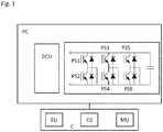
- Figure 1 shows a block diagram of a power converter PC and an exemplary embodiment of a circuit C according to the improved concept.
- the power converter may for example comprise a plurality of power semiconductor devices PS1, PS2,..., PS6 (six are shown as exemplary number only; circuit symbols of an IGBT are used only as a placeholder for any power semiconductor device) and a drive and control unit DCU.
- the devices PS1,..., PS6 are depicted as part of a six-switch three-phase two-level inverter which is a standard application for a power converter.
- the Power converter PC further may comprise circuitry for generating a switching signal SS, for example a PWM signal.
- the PWM signal may be generated based on a PWM carrier signal.
- the carrier signal or the switching signal SS may be generated based on a base clock signal or system clock signal generated for example by a base clock generator (not shown) of the power converter PC.
- the circuit C is for example arranged outside of the power converter PC and coupled to the power converter PC.
- the circuit C comprises an evaluation unit EU and a measuring unit MU.
- the circuit comprises a clock generator CG.
- the circuit C may comprise a storage unit (not shown).
- circuit C The operation of the circuit C is explained with respect to an exemplary implementation of a method according to the improved concept as depicted in Figure 2 .
- the clock generator CG provides a sample clock signal SC with a constant sample frequency.
- a sample clock signal SC with a constant sample frequency.
- the sample clock signal SC may be asynchronous to or independent of an operation of the power converter PC, for example of the base clock signal or the switching signal SS.
- the measuring unit MU is configured to determine operating parameters of one of the power semiconductor devices PS1,..., PS6, for example of the device PS1, during each of the sample intervals S1,..., S7.
- the operating parameters include an on-state voltage V on , an on-state current I on and an off-state voltage V off of the device PS1.
- the operating parameters may include a total number of turn-on events N on and a total number of turn-off events N off within a sample interval.
- a turn-on event is a switching event from logic zero to logic one of the switching signal SS
- a turn-off event is a switching event from logic one to logic zero of the switching signal SS.
- some of the operating parameters may be measured during or at the end of the sample interval or may be taken from a preceding sample interval. This is described in the following exemplarily with respect to Figure 2 .
- the switching signal SS begins with an on-state and has one turn-off event. Since the on-state current I on is stable after a very short time period after the turn-on event, I on is measured during interval S1. Alternatively, the on-state current I on may be taken from a previous sample interval (not shown). Compared to the current, the on-state voltage V on requires a longer time period after the turn-on event. Therefore, for example, the on-state voltage V on , is not measured during S1 but taken from the previous sample interval. Note that the on-state voltage V on could also be measured during S1 if the width of the respective on-state pulse is sufficiently large.
- the turn-off voltage V off is measured during S1, for example at or directly after the turn-off event.
- the switching signal SS begins with an off-state and has no turn-on event. Therefore, the switching and conduction energies E sw , E c are both zero.
- the on-state current and voltage I on , V on cannot be determined for interval S2 by definition.
- the off-state voltage V off may optionally be measured.
- the switching signal SS begins with an off-state and has one turn-on event.
- all three of the on-state current and voltage I on , V on and the off-state voltage V off may be measured during S3.
- the off-state voltage V off may be taken for example from interval S2.
- the switching and conduction energies E sw , E c may be determined as described above.
- the on-state voltage V on may be taken for example from interval S1. This may be advantageous in case the on-state duration within S3 after the turn-on event in S3 is too short for the on-state voltage V on to settle.
- the switching signal SS begins with an on-state and has no turn-off event. Therefore, the off-state voltage V off cannot be determined for interval S4 by definition and the switching energy E sw is zero.
- the on-state current and voltage I on , V on may be measured during S4 and the conduction energy E c may be determined as described above.
- the switching signal SS begins with an on-state and has one turn-off event followed by one turn-on event. Therefore, all three of the on-state current and voltage I on , V on and the off-state voltage V off may be measured during S5.
- the switching and conduction energies E sw , E c may be determined as described above.
- the on-state voltage V on may be taken for example from interval S4. This may be advantageous in case the on-state duration within S5 after the second turn-on event in S5 is too short for the on-state voltage V on to settle.
- the switching signal SS begins with an on-state and has a turn-off event followed by a turn-on event and another turn-off event. Therefore, all three of the on-state current and voltage I on , V on and the off-state voltage V off may be measured during S6.
- the switching and conduction energies E sw , E c may be determined as described above.
- the on-state voltage V on may be taken for example from interval S5. This may be advantageous in case the on-state duration within S5 after the second turn-on event in S5 is too short for the on-state voltage V on to settle.
- the switching signal SS begins with an off-state and has a turn-on event followed by a turn-off event and another turn-on event. Therefore, all three of the on-state current and voltage I on , V on and the off-state voltage V off may be measured during S7.
- the switching and conduction energies E sw , E c may be determined as described above.
- the on-state voltage V on may be taken for example from interval S6. This may be advantageous in case the first on-state duration after the first turn-on event in S7 and the second on-state duration within S7 after the second turn on-event both are too short for the on-state voltage V on to settle.
- the conduction and switching power loss P c , P sw may be determined for each of the sample intervals S1,..., S7 independently from the base clock of the power converter PC.
- the conduction and switching power loss P c , P sw may be added up by the evaluation unit EU to obtain a self-heating power loss P sh of the power semiconductor device PS1, which may be used as an input to a thermal model.
- the output of the thermal model may be used to determine the junction temperature of the power semiconductor device PS1.
- a cross-coupling power loss may be determined, for example by the evaluation unit EU, and be used as an additional input to the thermal model to improve accuracy.
- the cross-coupling power loss may result from further devices of the power converter PC, for example the further semiconductor devices PS2,..., PS6, and their effect on the junction temperature of the power semiconductor device PS1.
- an operating condition of a power converter in particular a junction temperature of a power semiconductor device of the power converter, may be determined in a universal manner applicable to a great variety of power converters.
- the improved concept is compatible with any switching scheme of the power converter, including regular PWM, for example sine PWM, third harmonic injection, space-vector PWM, discontinuous PWM, for example over-modulation, multi-level converters, irregular PWM, for example direct torque control, hysteresis control, line-frequency switching, for example modular multi-level applications, high-speed motor drive operation or DC choppers, for example buck and boost DC-DC converters.
- regular PWM for example sine PWM, third harmonic injection, space-vector PWM, discontinuous PWM, for example over-modulation, multi-level converters, irregular PWM, for example direct torque control, hysteresis control, line-frequency switching, for example modular multi-level applications, high-speed motor drive operation or DC choppers, for example buck and boost DC-DC converters.
- the improved concept is compatible with a wide range of switching frequencies of the power converter, for example hundreds of Hz to tens of kHz. Even as low frequencies as the modulation frequency in the range of 50-200 Hz are possible.
- the improved concept may be further enhanced by determining the same operating parameter twice or more often during a given sample interval and calculating a respective average or other aggregate value for the power loss calculation. This may improve the accuracy in case of high frequency switching applications.
- Implementations according to the improved concept may involve junction temperature estimation of a power semiconductor device, which may enable several features in next generation of "smart" power converters, including: dynamic rating control (intelligent over-rate/de-rate), optimized parallel inverter stack current sharing, condition monitoring (detection of wear-out and abnormal operation, giving predictive maintenance), temperature cycle counting and remaining useful life estimation, improved validation of inverter stack design during development and type testing, improved over-temperature detection.
- dynamic rating control intelligent over-rate/de-rate
- optimized parallel inverter stack current sharing condition monitoring (detection of wear-out and abnormal operation, giving predictive maintenance)
- temperature cycle counting and remaining useful life estimation
- improved validation of inverter stack design during development and type testing improved over-temperature detection.
Landscapes
- Engineering & Computer Science (AREA)
- Power Engineering (AREA)
- Physics & Mathematics (AREA)
- General Physics & Mathematics (AREA)
- Microelectronics & Electronic Packaging (AREA)
- Inverter Devices (AREA)
- Power Conversion In General (AREA)
- Testing Of Individual Semiconductor Devices (AREA)
Priority Applications (6)
| Application Number | Priority Date | Filing Date | Title |
|---|---|---|---|
| EP18196074.1A EP3627675A1 (fr) | 2018-09-21 | 2018-09-21 | Analyse des conditions de fonctionnement d'un convertisseur de puissance |
| US17/276,877 US11735993B2 (en) | 2018-09-21 | 2019-09-19 | Analyzing an operating condition of a power converter |
| PCT/EP2019/075228 WO2020058436A1 (fr) | 2018-09-21 | 2019-09-19 | Analyse d'une condition de fonctionnement d'un convertisseur de courant |
| JP2021515556A JP2022501991A (ja) | 2018-09-21 | 2019-09-19 | 電力変換器の動作状況の分析 |
| KR1020217011115A KR102773298B1 (ko) | 2018-09-21 | 2019-09-19 | 전력 변환기의 동작 상태의 분석 기술 |
| CN201980061430.5A CN112740524B (zh) | 2018-09-21 | 2019-09-19 | 分析功率转换器的操作状况 |
Applications Claiming Priority (1)
| Application Number | Priority Date | Filing Date | Title |
|---|---|---|---|
| EP18196074.1A EP3627675A1 (fr) | 2018-09-21 | 2018-09-21 | Analyse des conditions de fonctionnement d'un convertisseur de puissance |
Publications (1)
| Publication Number | Publication Date |
|---|---|
| EP3627675A1 true EP3627675A1 (fr) | 2020-03-25 |
Family
ID=63678541
Family Applications (1)
| Application Number | Title | Priority Date | Filing Date |
|---|---|---|---|
| EP18196074.1A Ceased EP3627675A1 (fr) | 2018-09-21 | 2018-09-21 | Analyse des conditions de fonctionnement d'un convertisseur de puissance |
Country Status (6)
| Country | Link |
|---|---|
| US (1) | US11735993B2 (fr) |
| EP (1) | EP3627675A1 (fr) |
| JP (1) | JP2022501991A (fr) |
| KR (1) | KR102773298B1 (fr) |
| CN (1) | CN112740524B (fr) |
| WO (1) | WO2020058436A1 (fr) |
Cited By (1)
| Publication number | Priority date | Publication date | Assignee | Title |
|---|---|---|---|---|
| WO2026077499A1 (fr) * | 2024-10-10 | 2026-04-16 | Schaeffler Technologies AG & Co. KG | Détermination d'énergies de perte de commutation dans des convertisseurs à commutation électronique de puissance |
Families Citing this family (3)
| Publication number | Priority date | Publication date | Assignee | Title |
|---|---|---|---|---|
| EP3875973B1 (fr) * | 2020-03-02 | 2024-05-08 | Maschinenfabrik Reinhausen GmbH | L'analyse du fonctionnement d'un dispositif semi-conducteur de puissance |
| ES3049763T3 (en) | 2021-05-20 | 2025-12-18 | Lg Energy Solution Ltd | Battery module with improved safety |
| CN117235999B (zh) * | 2023-09-07 | 2026-02-06 | 浙江大学 | 一种基于电流通路分析的dc/ac变换器损耗和结温计算方法 |
Citations (5)
| Publication number | Priority date | Publication date | Assignee | Title |
|---|---|---|---|---|
| DE19613735A1 (de) * | 1996-03-29 | 1997-10-02 | Siemens Ag | Verfahren zum Erzeugen eines einer elektrischen Wirkleistung proportionalen Meßsignals |
| EP2498391A1 (fr) * | 2009-11-02 | 2012-09-12 | Kabushiki Kaisha Toshiba | Dispositif onduleur |
| EP2657712A2 (fr) * | 2012-04-23 | 2013-10-30 | Guildline Instruments Limited | Système de mesure CA asynchrone |
| US9035633B1 (en) * | 2009-12-29 | 2015-05-19 | Sunpower Corporation | Switching power converter control |
| EP3373019A1 (fr) * | 2015-11-05 | 2018-09-12 | CRRC Zhuzhou Institute Co., Ltd. | Dispositif et procédé de gestion en ligne de santé de transistor bipolaire à grille isolée |
Family Cites Families (11)
| Publication number | Priority date | Publication date | Assignee | Title |
|---|---|---|---|---|
| JP3987953B2 (ja) * | 2001-04-20 | 2007-10-10 | サンケン電気株式会社 | ソレノイド駆動装置及び駆動方法 |
| CN1640084A (zh) * | 2002-03-04 | 2005-07-13 | St微电子公司 | 用于无线射频传输的谐振功率转换器及其方法 |
| US6819011B2 (en) * | 2002-11-14 | 2004-11-16 | Fyre Storm, Inc. | Switching power converter controller with watchdog timer |
| GB2403355A (en) * | 2003-06-24 | 2004-12-29 | Bombardier Transp | Current converter with variable switching repitition frequency |
| DE102006052042A1 (de) * | 2006-10-30 | 2008-05-15 | Bombardier Transportation Gmbh | Steuerung und/oder Regelung eines 3-Phasen-Stromrichters für den Betrieb einer Asynchronmaschine |
| US7764054B1 (en) * | 2008-05-21 | 2010-07-27 | Fairchild Semiconductor Corporation | Voltage regulator with current-mode dual-edge width modulation and non-linear control |
| CN103280971B (zh) * | 2013-05-28 | 2016-01-13 | 成都芯源系统有限公司 | 升降压变换器及其控制器和控制方法 |
| CN104065266B (zh) * | 2014-07-11 | 2017-12-15 | 成都芯源系统有限公司 | 用于电压转换器的控制电路 |
| US10033272B2 (en) * | 2015-03-12 | 2018-07-24 | Qualcomm Incorporated | Switching loss correction circuitry and method |
| JP6557517B2 (ja) * | 2015-06-08 | 2019-08-07 | ルネサスエレクトロニクス株式会社 | 半導体集積回路装置および電子装置 |
| US10644581B2 (en) * | 2017-11-01 | 2020-05-05 | Texas Instruments Incorporated | DC-DC power conversion circuitry with efficiency optimization using temperature sensing |
-
2018
- 2018-09-21 EP EP18196074.1A patent/EP3627675A1/fr not_active Ceased
-
2019
- 2019-09-19 US US17/276,877 patent/US11735993B2/en active Active
- 2019-09-19 JP JP2021515556A patent/JP2022501991A/ja active Pending
- 2019-09-19 WO PCT/EP2019/075228 patent/WO2020058436A1/fr not_active Ceased
- 2019-09-19 CN CN201980061430.5A patent/CN112740524B/zh active Active
- 2019-09-19 KR KR1020217011115A patent/KR102773298B1/ko active Active
Patent Citations (5)
| Publication number | Priority date | Publication date | Assignee | Title |
|---|---|---|---|---|
| DE19613735A1 (de) * | 1996-03-29 | 1997-10-02 | Siemens Ag | Verfahren zum Erzeugen eines einer elektrischen Wirkleistung proportionalen Meßsignals |
| EP2498391A1 (fr) * | 2009-11-02 | 2012-09-12 | Kabushiki Kaisha Toshiba | Dispositif onduleur |
| US9035633B1 (en) * | 2009-12-29 | 2015-05-19 | Sunpower Corporation | Switching power converter control |
| EP2657712A2 (fr) * | 2012-04-23 | 2013-10-30 | Guildline Instruments Limited | Système de mesure CA asynchrone |
| EP3373019A1 (fr) * | 2015-11-05 | 2018-09-12 | CRRC Zhuzhou Institute Co., Ltd. | Dispositif et procédé de gestion en ligne de santé de transistor bipolaire à grille isolée |
Cited By (1)
| Publication number | Priority date | Publication date | Assignee | Title |
|---|---|---|---|---|
| WO2026077499A1 (fr) * | 2024-10-10 | 2026-04-16 | Schaeffler Technologies AG & Co. KG | Détermination d'énergies de perte de commutation dans des convertisseurs à commutation électronique de puissance |
Also Published As
| Publication number | Publication date |
|---|---|
| KR20210065127A (ko) | 2021-06-03 |
| JP2022501991A (ja) | 2022-01-06 |
| KR102773298B1 (ko) | 2025-02-25 |
| CN112740524B (zh) | 2024-12-10 |
| US20220037993A1 (en) | 2022-02-03 |
| WO2020058436A1 (fr) | 2020-03-26 |
| CN112740524A (zh) | 2021-04-30 |
| US11735993B2 (en) | 2023-08-22 |
Similar Documents
| Publication | Publication Date | Title |
|---|---|---|
| US11735993B2 (en) | Analyzing an operating condition of a power converter | |
| Alvarez et al. | Sinusoidal current operation of delay-time compensation for parallel-connected IGBTs | |
| Khaligh et al. | Dead-time distortion in generalized selective harmonic control | |
| Pu et al. | Real-time degradation monitoring of SiC-MOSFETs through readily available system microcontroller | |
| Kouro et al. | Switching loss analysis of modulation methods used in cascaded H-bridge multilevel converters | |
| Langmaack et al. | Fast and universal semiconductor loss calculation method | |
| Arnaudov et al. | Modeling of multiphase converter for charging of energy storage elements | |
| Pietrowski et al. | The wide range of output frequency regulation method for the inverter using the combination of PWM and DDS | |
| HK40049010A (en) | Analyzing an operating condition of a power converter | |
| Swamy et al. | Speed control of space vector modulated inverter driven induction motor | |
| Edrington et al. | Power semiconductor loss evaluation in voltage source IGBT converters for three-phase induction motor drives | |
| Kaboli et al. | Probabilistic voltage harmonic analysis of direct torque controlled induction motor drives | |
| Das et al. | Experimental study on the influence of junction temperature on the relationship between IGBT switching energy loss and device current | |
| Albu et al. | Single-phase SPWM inverter ordered with microcontroller | |
| Gai et al. | Comparative analysis of power losses in different PWM techniques for a three-phase voltage source inverter | |
| Wu et al. | Discrete-time modeling and stability analysis of grid-connected inverter based on equivalent circuit | |
| Cataliotti et al. | A new over modulation strategy for high-switching frequency space vector PWM voltage source inverters | |
| Liu et al. | Design and implementation of DSP based high-frequency SPWM generator | |
| Yankov et al. | A power loss analysis of a three-phase 12/8 switched reluctance motor fed from asymmetric power converter in MATLAB/Simulink | |
| Xiao et al. | An Improved SiC MOSFET Analytical Model for Multi-timescale Simulation and Loss Analysis of Power Electronic Systems | |
| Vuchev et al. | Comparative Analysis of Resonant Converters for Energy Storage Systems | |
| Montazeri Najafabadi | Efficiency Optimization of Induction Machine Drives with Model Predictive Control | |
| Anjana et al. | Investigation into the Reverse Recovery Dynamics of High-Voltage Fast Recovery Diodes | |
| Khelif et al. | Diagnosis of SVM controlled three-phase rectifier using mean value of park currents technique | |
| Haspel et al. | A Simple Approach to Realize a Power Hardware-in-the-Loop Machine Emulator Based on a B6-Inverter and a Bang-Bang Controller |
Legal Events
| Date | Code | Title | Description |
|---|---|---|---|
| PUAI | Public reference made under article 153(3) epc to a published international application that has entered the european phase |
Free format text: ORIGINAL CODE: 0009012 |
|
| STAA | Information on the status of an ep patent application or granted ep patent |
Free format text: STATUS: THE APPLICATION HAS BEEN PUBLISHED |
|
| AK | Designated contracting states |
Kind code of ref document: A1 Designated state(s): AL AT BE BG CH CY CZ DE DK EE ES FI FR GB GR HR HU IE IS IT LI LT LU LV MC MK MT NL NO PL PT RO RS SE SI SK SM TR |
|
| AX | Request for extension of the european patent |
Extension state: BA ME |
|
| STAA | Information on the status of an ep patent application or granted ep patent |
Free format text: STATUS: REQUEST FOR EXAMINATION WAS MADE |
|
| 17P | Request for examination filed |
Effective date: 20200925 |
|
| RBV | Designated contracting states (corrected) |
Designated state(s): AL AT BE BG CH CY CZ DE DK EE ES FI FR GB GR HR HU IE IS IT LI LT LU LV MC MK MT NL NO PL PT RO RS SE SI SK SM TR |
|
| STAA | Information on the status of an ep patent application or granted ep patent |
Free format text: STATUS: EXAMINATION IS IN PROGRESS |
|
| 17Q | First examination report despatched |
Effective date: 20210715 |
|
| STAA | Information on the status of an ep patent application or granted ep patent |
Free format text: STATUS: THE APPLICATION HAS BEEN REFUSED |
|
| 18R | Application refused |
Effective date: 20230702 |