EP2498391A1 - Dispositif onduleur - Google Patents
Dispositif onduleur Download PDFInfo
- Publication number
- EP2498391A1 EP2498391A1 EP10826755A EP10826755A EP2498391A1 EP 2498391 A1 EP2498391 A1 EP 2498391A1 EP 10826755 A EP10826755 A EP 10826755A EP 10826755 A EP10826755 A EP 10826755A EP 2498391 A1 EP2498391 A1 EP 2498391A1
- Authority
- EP
- European Patent Office
- Prior art keywords
- temperature
- switching elements
- loss
- switching
- inverter
- Prior art date
- Legal status (The legal status is an assumption and is not a legal conclusion. Google has not performed a legal analysis and makes no representation as to the accuracy of the status listed.)
- Granted
Links
Images


Classifications
-
- H—ELECTRICITY
- H02—GENERATION; CONVERSION OR DISTRIBUTION OF ELECTRIC POWER
- H02M—APPARATUS FOR CONVERSION BETWEEN AC AND AC, BETWEEN AC AND DC, OR BETWEEN DC AND DC, AND FOR USE WITH MAINS OR SIMILAR POWER SUPPLY SYSTEMS; CONVERSION OF DC OR AC INPUT POWER INTO SURGE OUTPUT POWER; CONTROL OR REGULATION THEREOF
- H02M7/00—Conversion of AC power input into DC power output; Conversion of DC power input into AC power output
- H02M7/42—Conversion of DC power input into AC power output without possibility of reversal
- H02M7/44—Conversion of DC power input into AC power output without possibility of reversal by static converters
- H02M7/48—Conversion of DC power input into AC power output without possibility of reversal by static converters using discharge tubes with control electrode or semiconductor devices with control electrode
-
- B—PERFORMING OPERATIONS; TRANSPORTING
- B60—VEHICLES IN GENERAL
- B60L—PROPULSION OF ELECTRICALLY-PROPELLED VEHICLES; SUPPLYING ELECTRIC POWER FOR AUXILIARY EQUIPMENT OF ELECTRICALLY-PROPELLED VEHICLES; ELECTRODYNAMIC BRAKE SYSTEMS FOR VEHICLES IN GENERAL; MAGNETIC SUSPENSION OR LEVITATION FOR VEHICLES; MONITORING OPERATING VARIABLES OF ELECTRICALLY-PROPELLED VEHICLES; ELECTRIC SAFETY DEVICES FOR ELECTRICALLY-PROPELLED VEHICLES
- B60L3/00—Electric devices on electrically-propelled vehicles for safety purposes; Monitoring operating variables, e.g. speed, deceleration or energy consumption
- B60L3/0023—Detecting, eliminating, remedying or compensating for drive train abnormalities, e.g. failures within the drive train
- B60L3/003—Detecting, eliminating, remedying or compensating for drive train abnormalities, e.g. failures within the drive train relating to inverters
-
- H—ELECTRICITY
- H02—GENERATION; CONVERSION OR DISTRIBUTION OF ELECTRIC POWER
- H02M—APPARATUS FOR CONVERSION BETWEEN AC AND AC, BETWEEN AC AND DC, OR BETWEEN DC AND DC, AND FOR USE WITH MAINS OR SIMILAR POWER SUPPLY SYSTEMS; CONVERSION OF DC OR AC INPUT POWER INTO SURGE OUTPUT POWER; CONTROL OR REGULATION THEREOF
- H02M1/00—Details of apparatus for conversion
- H02M1/32—Means for protecting converters other than automatic disconnection
- H02M1/327—Means for protecting converters other than automatic disconnection against abnormal temperatures
Definitions
- Embodiments of the present invention generally relate to an inverter apparatus, which drives an electric motor, and particularly to a technology for estimating a temperature of a switching element forming part of an inverter.
- An electric motor is used in a hybrid car in combination with an engine or in an electric car which is driven only by an electric motor.
- an inverter is used to obtain desired torque and frequency.
- the inverter is built in a car and is demanded to achieve high power at high integration density to ensure a passenger space.
- an operation temperature of the inverter greatly changes.
- the inverter has a high temperature under influence of heat generation of an engine.
- Switching elements in the inverter have a risk that the temperature increases under influence of constant loss due to a current through the switching elements themselves and switching loss due to switching on/off, in addition to influence of such an environmental temperature, and a breakdown may occur when a certain temperature is exceeded.
- the temperatures of the switching elements need to be detected for protection. Since temperature detection can be performed with high accuracy by using an on-chip sensor in which a diode is assembled in an element, such a sensor is mounted on an inverter for a hybrid car. Since the on-chip sensor has a high electric potential, temperature information needs to be transferred to a micro-controller (hereinafter abbreviated as mi-con) through an insulating circuit. In an inverter on which at least six switching elements are mounted, a plurality of insulating circuits are required to detect temperatures of all the switching elements. A board area increases and may cause an inverter capacity to increase.
- a method can be considered in which temperature detection is performed only partially on several of the switching elements and temperatures of the other switching elements are estimated. There has been disclosed a method in which one or more switching element temperatures are detected and a temperature of a switching element having a maximum temperature is estimated from thermal transfer models of IGBT modules.
- Patent Literature 1 Jpn. Pat. Appln. KOKAI Publication No. 2007-195343
- loss models of switching elements and thermal transfer models belong to a steady state.
- a state in which a current concentrates only on a part of the switching elements e.g., when a motor is locked or rotates at a low frequency
- a switching element which has a maximum temperature can not steadily be specified, and switching element temperatures can not accurately be estimated, either.
- thermal transfer models are constructed on the basis of estimated temperature values of switching elements existing around a switching element which is estimated to have the maximum temperature. Therefore, when a basing switching element temperature includes an error, an estimation error concerning the switching element temperature indicating the maximum temperature increases.
- the present invention has been made to solve problems as described above, and has an object of reducing the number of components forming an inverter apparatus and reducing a board space by accurately estimating temperatures of the other switching elements, based on a temperature detected from one switching element, whatever state an operation mode of the inverter is in.
- an inverter apparatus includes: a direct-current power supply; switching elements and a freewheel diode which are connected to the direct-current power supply; a means which converts a direct current voltage into a predetermined alternating current voltage, a predetermined current, and a predetermined frequency, depending on switching on/off of the switching elements; a temperature detector provided near at least one of the switching elements and an estimation means.
- the estimation means estimates temperatures of switching elements not provided with the temperature detector and the freewheel diode, based on a loss model of the switching elements and freewheel diode, a thermal resistance model of a module which fixes the switching elements and freewheel diodes, an estimated-temperature increase value calculated by the loss model and thermal resistance model, and a temperature of the switching element detected by the temperature detector.
- FIG. 1 shows a configuration of an embodiment when an inverter apparatus according to the invention is applied to an electric vehicle such as an electric car or a hybrid car.
- the inverter apparatus according to the invention can be applied not only to an electric vehicle but also to an electric propulsion ship.
- the inverter apparatus inputs a torque command value Tq* to an inverter 2 from an accelerator 1, and converts an output voltage of a direct current voltage source 4 such as a battery into a three-phase alternating-current voltage having a variable voltage and a variable frequency, depending on the torque command value Tq*, thereby to control wheels 6 by driving an electric motor 5.
- a direct current voltage source 4 such as a battery
- a condenser 7 which smoothes a direct current voltage is connected to an input stage, and bridged circuits of a U-phase, a V-phase, and a W-phase are formed by switching elements.
- a connection point between a switching element S U and a switching element S X is connected to an electric motor 5.
- the switching elements S U and S X are respectively connected in antiparallel with return diodes D U and D X .
- the bridge circuit of the V-phase which is formed by the switching elements S V and S Y and the return diodes D V and D Y
- the bridge circuit of the W-phase which is formed by the switching elements S W and S Z and the return diodes D W and D Z
- the bridge circuit of the V-phase which is formed by the switching elements S W and S Z and the return diodes D W and D Z
- a temperature sensor is provided near one or a plurality of the switching elements S U , S X , S V , S Y , S W , and S Z .
- temperature sensors C X , C Y , and C Z are respectively provided as low-side elements of the switching elements S X , S Y , and S Z .
- the temperature sensors C X , C Y , and C Z are on-chip diodes built on the switching elements. Under condition of a constant current, diodes have a tendency that a forward voltage decreases as a temperature increases.
- a temperature of a switching element is obtained by supplying a constant current for a diode and by measuring a forward voltage.
- Temperature sensors of a type other than diodes are applicable as the temperature sensors although the sensor desirably has high responsibility and accuracy.
- a temperature signal 9 of a switching element which indicates the highest temperature among the switching elements is transmitted to a control calculation apparatus 10.
- the switching elements S X , S Y , and S Z which form a lower leg (also referred to as an arm) of the inverter have equal potentials and need not be isolated from each other. Therefore, a temperature signal indicating a maximum temperature T NMAX can be easily extracted.
- FIG. 2 shows an example of a circuit 8a to select the maximum temperature T NMAX ⁇
- the present circuit is generally used as a minimum value circuit formed of operation amplifiers 11X, 11Y, and 11Z and diodes 12X, 12Y, and 12Z, and the lowest voltage among temperature sensor voltages V fX , V fY , and V fZ . Circle marks marked at operation amplifier inputs respectively represent inverted input terminals. A forward voltage of a diode decreases as a temperature thereof increases. Therefore, the lowest voltage is a signal which indicates the maximum temperature T NMAX .
- Output voltages are compared with an output of a triangular wave generation circuit 13 by a comparator 14, and are converted into pulses which are transferred to a control operation apparatus 10 through an insulating element 15 such as a photocoupler.
- the maximum temperature T NMAX is obtained by calculating a duty ratio of pulses with a control operation apparatus 10.
- FIG. 2 shows a circuit which is configured such that a duty decreases as a temperature increases. If one signal is thus transferred, one insulating element is enough for use in the temperature detection circuit 8, and a circuit scale need not be enlarged. Although one of temperatures of the switching elements S X , S Y , and S Z may be constantly detected, a more highly reliable temperature protection system can be provided by detecting the maximum temperature.
- the control operation apparatus 10 is formed of a current controller 16 and a temperature estimator 17.
- the current controller 16 is input with an instantaneous three-phase-current value 19 obtained from a current detector 18 and an electric angle 21 obtained from an angle detector 20 of an electric motor.
- a current command value corresponding to the torque command value Tqb* is calculated by the current controller 16, and a gate signal 22 with which a desired current can be obtained is output to a gate drive circuit 23.
- the gate drive circuit 23 is connected to all the gates that the switching elements S U , S V , S Y , S W , and S Z have, and switches on/off them, in accordance with the gate signal 22 input from the control operation apparatus 10.
- the temperature estimator 17 is input with the instantaneous three-phase-current voltage 19, a voltage value 25 obtained from the direct current voltage detector 24, and a maximum switching-element temperature 9 among switching element temperatures obtained from the temperature sensors C X , C Y , and C Z . Based on these physical amounts, temperatures of all the switching elements and return diodes are estimated.
- FIG. 3 is a flowchart showing an outline of a temperature estimation method which is carried out by the temperature estimator 17.
- the temperature estimator 17 estimates losses of all the elements of the IGBT and return diodes (FWD), based on IGBT temperatures, direct current voltages, phase currents, duty ratios, and carrier frequencies (S10).
- the temperature estimator 17 estimates temperature increase values of all the elements of IGBT and FWD elements, by inputting the losses to an IGBT-module heat-resistance model (S20).
- the temperature estimator 17 calculates temperatures from differences between the temperature increase estimation values and detected temperatures (S30). Using a detected temperature of an IGBT as a base, temperatures of other elements whose temperatures have not yet been detected are calculated.
- the temperature of each element depends on heat generated by a loss of the element itself and heat caused by losses of peripheral elements. Therefore, loss of each element needs to be estimated at first.
- Losses of the switching elements can be classified into conduction losses and switching losses.
- a conduction loss is caused by a current flowing through an element and a resistance component of the element itself, and depends on a junction temperature. Therefore, the conduction loss is expressed by Expression 1, below.
- P sat f I C T j ⁇ DUTY
- I C current flowing through an element (instant value)
- T j junction temperature of an element
- DUTY conduction rate of a switching element
- the current I C can be obtained from a current detector 18.
- Tj is a temperature to estimate from now and can therefore not be obtained.
- the maximum temperature T NMAX of an element in a low side which has been detected by a temperature sensor, is applied to all the elements. In the present embodiment, estimation is carried out not based on an average temperature but based on the maximum temperature for expectation of safety.
- a function f is expressed as a polynomial using a current I C and a temperature Tj, and is prestored in a control operation apparatus 10.
- a switching loss is a sum of an on-loss PSWON caused at the time of turn-on and an off-loss PSWOFF caused at the time of turn-off.
- Overlapping of a voltage and a current i.e., simultaneous generation of a voltage and a current in a switching element causes a loss.
- These losses depend on the junction temperature Tj, and are therefore expressed by Expressions 2 and 3, respectively.
- P SWON g I C V DC T j ⁇ f SW
- P SWOFF h I C V DC T j ⁇ f SW
- the voltage V DC is obtained from the voltage detector 24.
- These functions g and h can be described as polynomials of parameters, and are stored in the control operation apparatus 10. Like conduction losses, switching losses are not caused unless a current flows through an element.
- a conduction loss and a switching loss are obtained from each of the switching elements S U to S Z .
- a sum of the conduction loss and the switching loss is a loss caused by one element.
- a freewheel diode is provided in order to prevent a surge voltage to be generated when the switching element turns off. Therefore, a current flows through the freewheel diode during an off-period of the switching element. During an on-period of the switching element, no current flows through the freewheel diode.
- a loss of the freewheel diode is calculated as a sum of a conduction loss and a recovery loss.
- DUTY is a conduction rate of paired switching elements (for example, the switching element S X relative to the freewheel diode D U ).
- a function j is a polynomial formed of three parameters. Unless a current flows through a freewheel diode, no switching loss is caused. A detailed description will now be made, exemplifying the U-phase leg.
- a conduction loss and a recovery loss are obtained for each of return diodes D U to D Z .
- a total of the conduction loss and the recovery loss is a loss caused by one freewheel diode.
- the loss estimation method as described above is available.
- a calculation time required for estimating losses and temperatures is not sufficiently short, in comparison with the drive frequency. For example, when a cycle of a drive signal frequency is equal to the calculation time, equal detection current values are used for each calculation cycle. Therefore, accuracy of loss estimation remarkably deteriorates.
- An on-loss P SWON , an off-loss P SWOFF , and a recovery loss P trr are obtained by supposing an average current value as I ave 2 ⁇ 2 ⁇ I rms ⁇ by substituting this value for I C in Expressions 2, 3, and 5, and by further halving.
- Switching of the loss calculation method is determined by an electric frequency obtained by an angle detector.
- an electric frequency is smaller than a frequency f e
- an instantaneous current value is used for loss estimation
- an effective current value I rms is used for loss estimation.
- the cycle of the frequency f e is sufficiently shorter than a calculation cycle and a heat/time constant of the switching elements.
- P LOSS is a loss of a target for which the temperature increase ⁇ T j is calculated.
- modules are formed to be adjacent to other semiconductor elements in many cases, and are therefore influenced by losses generated from the other semiconductor elements. Accordingly, the temperature increases. That is, highly accurate temperature estimation requires obtaining a temperature increase to be obtained by considering the influence of the other semiconductor elements.
- Z th is called the thermal transfer impedance, and is determined by the shape and a material of a module formed by switching elements and return diodes. That is, the thermal transfer impedance Z th is obtained by a simulation or an experiment.
- Z th is expressed in form of Expression 8, below.
- R th is called the thermal resistance and is a constant expressing the relationship between a loss and a temperature increase in a steady state.
- ⁇ is a heat/time constant indicating the ratio of temperature increase to elapsed time in a transition state.
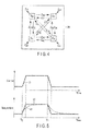
- FIG. 4 An example configuration of a semiconductor module is shown in FIG. 4 , and an estimation method for estimating a temperature increase will be described with reference to the figure.
- a semiconductor element forming a U-phase leg is mounted as an example on a semiconductor module 26 in FIG. 4 , which shows the relationship between each semiconductor element and a thermal transfer impedance.
- Expression 9 is satisfied, provided that switching elements S U and S X and return diodes D U and D X are respectively set as ⁇ T SU , ⁇ T SX , ⁇ T DU , and ⁇ T DX .
- Thermal transfer impedances Z ij all comply with the form of Expression 8, and values of the thermal resistance R th , the heat/time constant ⁇ , and the natural number n are determined by a shape and a material of the module 26 and by positions where semiconductor elements are provided. These Z ij are prestored in the control operation apparatus 10. ⁇ T SU 1 P SU ⁇ T SX 2 P SX ⁇ T DU 3 P DU ⁇ T DX 4 P DX
- the junction temperature input to the control operation apparatus 10 is a maximum temperature T NMAX of low-side elements.
- T NMAX T a + ⁇ T NMAX
- ⁇ T NMAX is the greatest value among the temperature increase values ⁇ T SX , ⁇ T SY , and ⁇ T SZ of respective phases, which are calculated for low-side switching elements of respective phases whose temperatures are measured by use of Expression 9.
- temperatures of all the switching elements and return diodes can be estimated.
- a temperature can be estimated by detecting a junction temperature for any one of all switching elements, in place of taking the maximum temperature T NMAX of the low-side elements as the temperature as a reference.
- reliability improves by using the maximum temperature.
- a switching element which takes the maximum temperature is estimated according to information of an electric angle obtained from an angle sensor.
- a module including return diodes complicates heat interference, and is therefore difficult to estimate a switching element whose maximum temperature only at an electric angle.
- the present application uses a heat interference model which takes a loss as a reference. Therefore, a temperature increase value can be accurately estimated, for phases other than a phase including an element (recording a maximum temperature) as a temperature detection target.
- the prior art configures a conventional thermal transfer impedance by thermal resistance components only, and therefore, cannot follow a temperature change in a transition state. For example, a description will now be made based on FIG. 5 .
- a current 27 increases at a time point of time T0
- an estimation temperature 29 abruptly increases, depending on a current in relation to a true temperature 28 which gently changes under the influence of actual thermal capacity. Therefore, the estimation temperature 29 is estimated to be higher than the true temperature 28.
- the estimation temperature decreases to be lower than the true temperature, and reliability is impaired.
- junction temperatures of all the switching elements and return diodes can be accurately estimated, without depending on the configuration, operation mode, and transition state of the module. Therefore, steady protection can be achieved, and an inverter apparatus with high reliability can be provided.
- Tj used in loss calculations through Expressions 1 to 5 is substituted with a maximum temperature T NMAX of the low-side elements detected by a temperature sensor.
- a temperature calculation is repeatedly performed for each control cycle T CTRL . Therefore, a temperature at present can be estimated by using an estimated temperature of each element obtained before the control cycle T CTRL .
- a loss (a value close to an actual value) can be more accurately estimated by using estimated temperatures of respective switching elements and return diodes which comply with actual situations than by uniquely using the maximum temperature T NMAX .
- the control cycle TCTRL needs to be sufficiently shorter than a heat/time constant to approximate a true temperature at the instance of estimation to an estimation temperature before the control cycle TCTRL used for estimation.
- the present embodiment is applied to a hybrid car of a sili-para system on which an inverter for driving an electric motor for driving and an inverter for a power generator driven by an engine are mounted. Since two inverters are mounted on the hybrid car of the sili-para system, the two inverters are integrated, in some cases, in order to reduce a mount space. At this time, semiconductor elements for the electric motor and semiconductor elements for the power generator are mounted on a module configured by semiconductor elements. Therefore, the semiconductor elements are influenced under heat generated from each other.
- the embodiments 1 and 2 relate to temperature estimation limited to an inverter for an electric motor. Under influence of heat generation from semiconductor elements for the power generator, as in the present embodiment, errors occur in temperature estimation.
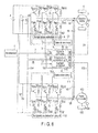
- FIG. 6 shows an example configuration of the present embodiment.
- the same configurations as those of the embodiment 1 will be denoted at the same reference signs, and reiterative descriptions will be omitted.
- the inverter which drives an electric motor 5 has exactly the same configuration as the embodiment 1.
- the inverter for the power generator comprises a condenser 101, switching elements S GU , S GV , S GV , S GX , S GY , and S GZ , and return diodes D GU , D GV , D GW , D GX , D GY , and D GZ .
- This inverter is connected to a power generator 103 driven by an engine 103, and returns electric power to a direct-current voltage source 4.
- a control operation apparatus 10 is added with a current controller 104 for a power generator.
- the current controller In accordance with a current instruction value I*105 which is instructed from a hybrid car, depending on a charge state of a battery (direct-current voltage source 4), the current controller generates a current value detected by a current sensor 106, and a gate signal 110 for switching elements, from an electric angle 109 detected by an angle sensor 108 of the power generator.
- the gate signal 110 is input to a gate drive circuit 111 to switch on/off a switching element.
- temperature detection of the inverter for the power generator is to detect an element having a maximum temperature in a low side.
- a temperature detection circuit 112 also has the same configuration as the temperature detection circuit 9 for the inverter for the electric motor.
- a temperature estimation unit 113 estimates junction temperatures of all the semiconductor elements of both inverters for the electric motor and power generator. Therefore, a current value 107 for the power generator and a maximum temperature element temperature 114 in the low side are used by the temperature estimation unit 113.
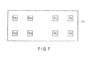
- an estimation method will be described. As shown in FIG. 7 in which a module 115 which integrates a U-phase of the inverter for the electric motor and a U-phase of the inverter for the power generator is an example, the number of semiconductor elements to be mounted is eight.
- a basic estimation method is the same as those in the embodiments 1 and 2 while only the number of elements as targets for temperature estimation increases.
- Loss of all elements are estimated by Expressions 1 to 5.
- a detection current used for loss estimation a current value 19 detected by a current sensor 18 is used for semiconductor elements in the side of the electric motor, and a current value 107 detected by a current sensor 106 is used for semiconductor elements in the side of the power generator.
- the thermal transfer impedance of Expression 8 is measured in advance.
- Expression 12 is used as an expression which expresses the relationship between a temperature increase and a loss in Expression 9.
- Temperature increase values of the semiconductor elements mounted on the modules of the V- and W-phases can also be obtained by using the same expression.
- junction temperatures are calculated in accordance with Expression 11.
- the maximum temperature T NMAX of low-side elements of an inverter for an electric motor is used as a reference.
- the present embodiment also takes T NMAX as a reference.
- low-side elements for the power generator are subjected to temperature detection.
- the semiconductor elements for the power generator are estimated by using Expression 11 with reference to the maximum temperature T NGMAX . That is, losses (P GSU -P GDX ) of the power generator of Expression 12 are obtained by using a maximum temperature in the loss Expressions 1 to 5.
- a temperature increase value ⁇ T is obtained from Expression 12, and the temperature increase value ⁇ T is substituted in Expression 11, to obtain a junction temperature.
- positions of a semiconductor element as a target for temperature estimation and an element which detects a temperature as a reference are set in a relationship to be close to each other. Then, the temperature estimation accuracy increases.
- Power generator 104... Current controller, 105... Current command value, 106... Current detector, 107 ... Current value, 108... Angle detector, 109... Electric angle, 110.,.
- Gate signal 111... Gate drive circuit, 112... Temperature detection circuit, 113... Temperature estimation unit, 114... Maximum low-side element temperature, 115... Semiconductor module
Landscapes
- Engineering & Computer Science (AREA)
- Power Engineering (AREA)
- Life Sciences & Earth Sciences (AREA)
- Sustainable Development (AREA)
- Sustainable Energy (AREA)
- Transportation (AREA)
- Mechanical Engineering (AREA)
- Inverter Devices (AREA)
- Electric Propulsion And Braking For Vehicles (AREA)
- Hybrid Electric Vehicles (AREA)
Applications Claiming Priority (2)
| Application Number | Priority Date | Filing Date | Title |
|---|---|---|---|
| JP2009252332A JP5443946B2 (ja) | 2009-11-02 | 2009-11-02 | インバータ装置 |
| PCT/JP2010/069035 WO2011052623A1 (fr) | 2009-11-02 | 2010-10-27 | Dispositif onduleur |
Publications (3)
| Publication Number | Publication Date |
|---|---|
| EP2498391A1 true EP2498391A1 (fr) | 2012-09-12 |
| EP2498391A4 EP2498391A4 (fr) | 2018-02-28 |
| EP2498391B1 EP2498391B1 (fr) | 2020-04-15 |
Family
ID=43922048
Family Applications (1)
| Application Number | Title | Priority Date | Filing Date |
|---|---|---|---|
| EP10826755.0A Active EP2498391B1 (fr) | 2009-11-02 | 2010-10-27 | Dispositif onduleur |
Country Status (5)
| Country | Link |
|---|---|
| US (1) | US8582335B2 (fr) |
| EP (1) | EP2498391B1 (fr) |
| JP (1) | JP5443946B2 (fr) |
| CN (1) | CN102474198B (fr) |
| WO (1) | WO2011052623A1 (fr) |
Cited By (4)
| Publication number | Priority date | Publication date | Assignee | Title |
|---|---|---|---|---|
| EP2768139A1 (fr) * | 2013-02-14 | 2014-08-20 | ABB Oy | Système de commande pour des commutateurs semiconducteurs |
| WO2015000651A1 (fr) * | 2013-07-03 | 2015-01-08 | Zf Friedrichshafen Ag | Dispositif de contrôle et procédé permettant de surveiller une fonction d'un composant semi-conducteur pendant le fonctionnement de ce dernier, et module électrique pourvu d'un dispositif de contrôle |
| EP3627675A1 (fr) * | 2018-09-21 | 2020-03-25 | Maschinenfabrik Reinhausen GmbH | Analyse des conditions de fonctionnement d'un convertisseur de puissance |
| WO2025195554A1 (fr) * | 2024-03-20 | 2025-09-25 | Schaeffler Technologies AG & Co. KG | Calcul dépendant de la fréquence de sortie de la température de jonction de semi-conducteurs de puissance dans un convertisseur de puissance |
Families Citing this family (70)
| Publication number | Priority date | Publication date | Assignee | Title |
|---|---|---|---|---|
| JP5633682B2 (ja) * | 2010-06-03 | 2014-12-03 | 日産自動車株式会社 | 電力変換機の制御装置 |
| CN103415992B (zh) * | 2011-02-25 | 2016-07-27 | Ntn株式会社 | 电动汽车 |
| JP5482694B2 (ja) * | 2011-03-08 | 2014-05-07 | 株式会社デンソー | 電力変換装置 |
| US9815193B2 (en) | 2011-06-27 | 2017-11-14 | Delaware Capital Formation, Inc. | Electric motor based holding control systems and methods |
| JP5546687B2 (ja) * | 2011-07-28 | 2014-07-09 | 三菱電機株式会社 | モータ制御装置 |
| JP5500136B2 (ja) * | 2011-08-18 | 2014-05-21 | 三菱電機株式会社 | 半導体電力変換装置 |
| CA2879578A1 (fr) * | 2012-08-03 | 2014-02-06 | Abb Schweiz Ag | Limitation de surcharge en fonctionnement de puissance de crete |
| JP2014036475A (ja) * | 2012-08-08 | 2014-02-24 | Hitachi Automotive Systems Ltd | 電動パワートレインシステム |
| JP5927082B2 (ja) * | 2012-08-28 | 2016-05-25 | 本田技研工業株式会社 | 電動機の駆動装置 |
| JP5843735B2 (ja) * | 2012-09-24 | 2016-01-13 | 三菱電機株式会社 | インバータの過熱保護制御装置及びインバータの過熱保護制御方法 |
| KR102062018B1 (ko) * | 2012-11-14 | 2020-01-08 | 현대로템 주식회사 | 철도차량용 보조전원장치의 제어회로 및 방법 |
| WO2014091852A1 (fr) * | 2012-12-12 | 2014-06-19 | 富士電機株式会社 | Dispositif d'estimation de température de puce de semi-conducteur et dispositif de protection contre une surchauffe |
| CN102991374B (zh) * | 2012-12-15 | 2017-07-21 | 奇瑞新能源汽车技术有限公司 | 一种电动汽车电机控制器被动整流保护系统 |
| JP6339022B2 (ja) * | 2012-12-28 | 2018-06-06 | 三菱電機株式会社 | 半導体装置、自動車 |
| JP2014187789A (ja) * | 2013-03-22 | 2014-10-02 | Fanuc Ltd | 異常検出機能を備えたモータ駆動装置 |
| US9891640B2 (en) * | 2013-06-14 | 2018-02-13 | Infineon Technologies Ag | Sensing element for semiconductor |
| CN103346712B (zh) * | 2013-07-24 | 2015-07-08 | 东南大学 | 一种在线估算低速电流斩波控制模式中开关磁阻电机控制器下续流管温度的方法 |
| CN103457495B (zh) * | 2013-09-13 | 2014-12-10 | 青岛四方车辆研究所有限公司 | 动车组辅助变流器有互联线并联供电控制系统及控制方法 |
| WO2015035803A1 (fr) | 2013-09-13 | 2015-03-19 | 青岛四方车辆研究所有限公司 | Système et méthode de commande d'alimentation électrique parallèle pour convertisseurs auxiliaires d'unité train de moteurs en présence de lignes d'interconnexion. |
| US9465074B2 (en) * | 2013-10-09 | 2016-10-11 | Ford Global Technologies, Llc | System and method for measuring switching loss associated with semiconductor switching devices |
| JP5907236B2 (ja) * | 2013-12-11 | 2016-04-26 | 株式会社デンソー | 温度検出装置 |
| JP6219154B2 (ja) | 2013-12-11 | 2017-10-25 | 新電元工業株式会社 | 温度検出装置 |
| KR102056156B1 (ko) | 2013-12-24 | 2019-12-16 | 현대자동차 주식회사 | 전기 차량의 인버터 보호 방법 |
| CN103701105A (zh) * | 2013-12-31 | 2014-04-02 | 深圳市英威腾电气股份有限公司 | 一种电力电子设备的热过载保护方法、装置及系统 |
| KR101646346B1 (ko) * | 2014-09-23 | 2016-08-05 | 현대자동차주식회사 | 모터 제어 장치 및 방법 |
| CN107306516B (zh) * | 2014-12-24 | 2019-08-20 | 东芝三菱电机产业系统株式会社 | 功率转换装置 |
| JP6091546B2 (ja) * | 2015-05-28 | 2017-03-08 | 三菱電機株式会社 | 回転電機制御装置 |
| JP6557517B2 (ja) | 2015-06-08 | 2019-08-07 | ルネサスエレクトロニクス株式会社 | 半導体集積回路装置および電子装置 |
| JP6549451B2 (ja) | 2015-09-02 | 2019-07-24 | ルネサスエレクトロニクス株式会社 | 半導体集積回路装置および電子装置 |
| US9608558B1 (en) * | 2015-09-14 | 2017-03-28 | Infineon Technologies Ag | Calculation of MOSFET switch temperature in motor control |
| JP2017060276A (ja) * | 2015-09-16 | 2017-03-23 | 富士電機株式会社 | 三相インバータ装置 |
| US9762146B2 (en) * | 2015-10-30 | 2017-09-12 | Faraday&Future Inc. | Methods and systems for interconnecting parallel IGBT modules |
| CA2947465A1 (fr) * | 2015-11-18 | 2017-05-18 | General Electric Company | Un systeme et une methode d'alimentation sans panne |
| CN108475997B (zh) * | 2015-12-10 | 2020-08-04 | 株式会社电装 | 信号传输电路 |
| CN108475998B (zh) * | 2015-12-18 | 2020-05-15 | 株式会社电装 | 电力转换装置的控制系统 |
| JP6332297B2 (ja) * | 2016-02-09 | 2018-05-30 | トヨタ自動車株式会社 | 電力変換装置 |
| JP6666174B2 (ja) * | 2016-03-10 | 2020-03-13 | 株式会社Soken | 電力変換装置 |
| CN105655984B (zh) * | 2016-03-28 | 2018-10-30 | 广州七喜智能设备有限公司 | 一种变频器中igbt过温保护方法 |
| JP6180576B1 (ja) * | 2016-04-12 | 2017-08-16 | 三菱電機株式会社 | Dc−dc電圧変換装置 |
| US10811985B2 (en) | 2016-08-26 | 2020-10-20 | General Electric Company | Power conversion system and an associated method thereof |
| US10309838B2 (en) * | 2016-09-08 | 2019-06-04 | Qualcomm Incorporated | Temporal temperature sensor position offset error correction |
| JP2018046647A (ja) * | 2016-09-14 | 2018-03-22 | サンデン・オートモーティブコンポーネント株式会社 | インバータ装置及びそれを備えた車両用電動圧縮機 |
| JP2018096888A (ja) * | 2016-12-15 | 2018-06-21 | ルネサスエレクトロニクス株式会社 | 電圧検出装置、それを備えた温度検出装置、電圧検出方法、及び、それを備えた温度検出方法 |
| KR102712333B1 (ko) * | 2016-12-15 | 2024-10-02 | 현대자동차주식회사 | 파워모듈의 정션온도 측정 방법 |
| WO2019053825A1 (fr) * | 2017-09-13 | 2019-03-21 | 三菱電機株式会社 | Dispositif et procédé de commande pour ascenseurs |
| CH714311A1 (de) * | 2017-11-08 | 2019-05-15 | Landis & Gyr Ag | Schaltsystem für einen Stromzähler und Verfahren zum Schalten eines Schalters. |
| JP6753837B2 (ja) * | 2017-12-18 | 2020-09-09 | 株式会社東芝 | インバータ装置、及びインバータ装置の放熱特性検出方法 |
| US11323032B2 (en) * | 2017-12-28 | 2022-05-03 | Shindengen Electric Manufacturing Co., Ltd. | Plural power modules conversion device with switch element control |
| JP6753883B2 (ja) * | 2018-03-19 | 2020-09-09 | 株式会社東芝 | 検査装置、検査方法、検査プログラムおよびインバータ装置 |
| JP7091800B2 (ja) * | 2018-04-16 | 2022-06-28 | 株式会社デンソー | 回路基板 |
| JP7061060B2 (ja) * | 2018-12-20 | 2022-04-27 | ルネサスエレクトロニクス株式会社 | 制御回路、駆動システムおよびインバータの制御方法 |
| DE102019101163B3 (de) * | 2019-01-17 | 2020-06-04 | Schaeffler Technologies AG & Co. KG | Elektrische Antriebseinheit und Verfahren zur Temperaturberechnung in einer elektrischen Antriebseinheit |
| CN110098635B (zh) * | 2019-04-17 | 2022-06-28 | 华为数字能源技术有限公司 | 一种光伏逆变器以及相应开关频率控制的方法 |
| DE102020002352A1 (de) * | 2019-04-25 | 2020-10-29 | Fanuc Corporation | Motorantriebsvorrichtung mit Energiespeicher |
| JP6847158B2 (ja) * | 2019-05-31 | 2021-03-24 | 三菱電機株式会社 | 電力変換装置 |
| JP7181851B2 (ja) * | 2019-12-13 | 2022-12-01 | 日立Astemo株式会社 | 電力変換装置 |
| KR20210129855A (ko) * | 2020-04-21 | 2021-10-29 | 현대자동차주식회사 | 무선 충전 장치, 차량용 무선 충전 시스템 및 그 제어 방법 |
| JP7472663B2 (ja) * | 2020-06-05 | 2024-04-23 | 富士電機株式会社 | 電力変換装置 |
| JP7494041B2 (ja) * | 2020-07-29 | 2024-06-03 | 株式会社日立産機システム | 電力変換装置および遠隔監視システム |
| JP7385538B2 (ja) * | 2020-07-31 | 2023-11-22 | 株式会社安川電機 | 電力変換装置、温度推定方法及びプログラム |
| DE112021003307T5 (de) * | 2020-08-25 | 2023-04-20 | Sanden Corporation | Wechselrichtervorrichtung und damit ausgerüsteter elektrischer kompressor für fahrzeuge |
| EP3979480A1 (fr) * | 2020-10-01 | 2022-04-06 | Siemens Aktiengesellschaft | Agencement et procédé de détermination des températures des composants électroniques |
| CN115603604A (zh) * | 2021-07-08 | 2023-01-13 | 法雷奥西门子新能源汽车德国有限责任公司(De) | 逆变器以及半导体开关的内部温度的估算 |
| CN114398809B (zh) * | 2021-12-17 | 2025-09-19 | 中车永济电机有限公司 | 一种考虑散热器的igbt模块结温计算方法 |
| WO2023190776A1 (fr) | 2022-03-29 | 2023-10-05 | ニデック株式会社 | Dispositif de conversion de puissance, programme d'estimation et procédé d'estimation |
| JP7254230B1 (ja) * | 2022-03-29 | 2023-04-07 | 三菱電機株式会社 | 電力変換装置 |
| DE102022208136A1 (de) * | 2022-08-04 | 2024-02-15 | Zf Friedrichshafen Ag | Verfahren und Vorrichtung zum Bestimmen einer Halbleitertemperatur eines Halbleiterelements, Stromrichter, elektrischer Achsantrieb und Kraftfahrzeug |
| CN118826584B (zh) * | 2023-12-26 | 2025-11-04 | 比亚迪股份有限公司 | 电机控制方法、存储介质、控制器及电机 |
| WO2025162313A1 (fr) * | 2024-01-31 | 2025-08-07 | 台达电子工业股份有限公司 | Appareil d'alimentation électrique |
| CN118584284B (zh) * | 2024-08-05 | 2025-07-01 | 清华大学 | 功率半导体特性测试回路、方法、系统、设备及存储介质 |
Family Cites Families (11)
| Publication number | Priority date | Publication date | Assignee | Title |
|---|---|---|---|---|
| JPH07234162A (ja) * | 1994-02-24 | 1995-09-05 | Toshiba Corp | 電力変換器の温度検出装置 |
| US6483271B1 (en) * | 2000-11-14 | 2002-11-19 | Otis Elevator Company | Motor drive parameters |
| US6747884B2 (en) * | 2001-04-13 | 2004-06-08 | Mitsubishi Denki Kabushiki Kaisha | Power converter device |
| JP4665569B2 (ja) * | 2004-11-30 | 2011-04-06 | トヨタ自動車株式会社 | 電圧変換装置および電圧変換装置における電圧変換の制御をコンピュータに実行させるためのプログラムを記録したコンピュータ読取り可能な記録媒体 |
| US7791300B2 (en) * | 2005-09-21 | 2010-09-07 | Mitsubishi Denki Kabushiki Kaisha | Excessive temperature detecting system of electric motor controller |
| JP4710588B2 (ja) * | 2005-12-16 | 2011-06-29 | トヨタ自動車株式会社 | 昇圧コンバータの制御装置 |
| JP2007195343A (ja) * | 2006-01-19 | 2007-08-02 | Nissan Motor Co Ltd | インバータ装置 |
| JP2009171702A (ja) * | 2008-01-15 | 2009-07-30 | Toyota Motor Corp | 車両駆動システム |
| JP2009229128A (ja) * | 2008-03-19 | 2009-10-08 | Hitachi Ltd | インバータ回路の温度センサ診断装置 |
| JP4703677B2 (ja) * | 2008-03-25 | 2011-06-15 | 三菱電機株式会社 | 車載用電力変換装置、及び車両制御装置 |
| US8148929B2 (en) * | 2008-09-30 | 2012-04-03 | Rockwell Automation Technologies, Inc. | Power electronic module IGBT protection method and system |
-
2009
- 2009-11-02 JP JP2009252332A patent/JP5443946B2/ja active Active
-
2010
- 2010-10-27 CN CN201080036867.2A patent/CN102474198B/zh active Active
- 2010-10-27 EP EP10826755.0A patent/EP2498391B1/fr active Active
- 2010-10-27 WO PCT/JP2010/069035 patent/WO2011052623A1/fr not_active Ceased
-
2012
- 2012-05-01 US US13/461,201 patent/US8582335B2/en active Active
Non-Patent Citations (1)
| Title |
|---|
| See references of WO2011052623A1 * |
Cited By (8)
| Publication number | Priority date | Publication date | Assignee | Title |
|---|---|---|---|---|
| EP2768139A1 (fr) * | 2013-02-14 | 2014-08-20 | ABB Oy | Système de commande pour des commutateurs semiconducteurs |
| WO2015000651A1 (fr) * | 2013-07-03 | 2015-01-08 | Zf Friedrichshafen Ag | Dispositif de contrôle et procédé permettant de surveiller une fonction d'un composant semi-conducteur pendant le fonctionnement de ce dernier, et module électrique pourvu d'un dispositif de contrôle |
| US10453767B2 (en) | 2013-07-03 | 2019-10-22 | ZF Friedricshafen AG | Control device and method for monitoring a function of a semiconductor component during the operation thereof and electrical assembly having a control device |
| EP3627675A1 (fr) * | 2018-09-21 | 2020-03-25 | Maschinenfabrik Reinhausen GmbH | Analyse des conditions de fonctionnement d'un convertisseur de puissance |
| WO2020058436A1 (fr) * | 2018-09-21 | 2020-03-26 | Maschinenfabrik Reinhausen Gmbh | Analyse d'une condition de fonctionnement d'un convertisseur de courant |
| CN112740524A (zh) * | 2018-09-21 | 2021-04-30 | 赖茵豪森机械制造公司 | 分析功率转换器的操作状况 |
| US11735993B2 (en) | 2018-09-21 | 2023-08-22 | Maschinenfabrik Reinhausen Gmbh | Analyzing an operating condition of a power converter |
| WO2025195554A1 (fr) * | 2024-03-20 | 2025-09-25 | Schaeffler Technologies AG & Co. KG | Calcul dépendant de la fréquence de sortie de la température de jonction de semi-conducteurs de puissance dans un convertisseur de puissance |
Also Published As
| Publication number | Publication date |
|---|---|
| JP5443946B2 (ja) | 2014-03-19 |
| EP2498391A4 (fr) | 2018-02-28 |
| CN102474198A (zh) | 2012-05-23 |
| CN102474198B (zh) | 2014-10-01 |
| JP2011097812A (ja) | 2011-05-12 |
| WO2011052623A1 (fr) | 2011-05-05 |
| EP2498391B1 (fr) | 2020-04-15 |
| US8582335B2 (en) | 2013-11-12 |
| US20120217795A1 (en) | 2012-08-30 |
Similar Documents
| Publication | Publication Date | Title |
|---|---|---|
| EP2498391B1 (fr) | Dispositif onduleur | |
| US8952642B2 (en) | Power conversion device and temperature rise calculation method thereof | |
| CN101494431B (zh) | 多相电动机控制装置 | |
| CN101983322B (zh) | 温度检测电路 | |
| CN102195551B (zh) | 用于五相机同步电流调整的方法、系统和设备 | |
| JP5578197B2 (ja) | 温度検出装置 | |
| US8878477B2 (en) | Electric motor driving apparatus having failure detection circuit, and failure detection method for the electric motor driving apparatus having failure detection circuit | |
| CN106410760A (zh) | 半导体集成电路装置及电子装置 | |
| EP3086453A1 (fr) | Convertisseur avec compensation des températures par un décalage cc de mode commun | |
| JP6217554B2 (ja) | インバータ装置 | |
| JP6398949B2 (ja) | 半導体素子の駆動装置 | |
| CN111092563B (zh) | 功率变换装置以及功率变换装置的诊断方法 | |
| US9991785B2 (en) | Electric power converting device | |
| CN102957333B (zh) | 半导体功率转换装置 | |
| EP3089346A1 (fr) | Dispositif de conversion de puissance et procédé de commande de dispositif de conversion de puissance | |
| JP2013258857A (ja) | 半導体モジュール及びその制御方法 | |
| US11290036B2 (en) | Control device | |
| US12237785B2 (en) | Electrical power conversion apparatus | |
| JP2015192578A (ja) | 電圧検出装置及び電圧電流検出装置 | |
| JP2017103840A (ja) | インバータ装置 | |
| JP2010154726A (ja) | 電力変換器の制御方法 | |
| JP5895704B2 (ja) | 電力変換装置 | |
| US20240377475A1 (en) | Method and device for detecting a short circuit of a semiconductor switch element in an inverter for energizing an electric drive in an electric vehicle or hybrid vehicle; inverter comprising such a device | |
| JP4631575B2 (ja) | インバータ装置 | |
| WO2025023028A1 (fr) | Convertisseur de puissance |
Legal Events
| Date | Code | Title | Description |
|---|---|---|---|
| PUAI | Public reference made under article 153(3) epc to a published international application that has entered the european phase |
Free format text: ORIGINAL CODE: 0009012 |
|
| 17P | Request for examination filed |
Effective date: 20120424 |
|
| AK | Designated contracting states |
Kind code of ref document: A1 Designated state(s): AL AT BE BG CH CY CZ DE DK EE ES FI FR GB GR HR HU IE IS IT LI LT LU LV MC MK MT NL NO PL PT RO RS SE SI SK SM TR |
|
| DAX | Request for extension of the european patent (deleted) | ||
| RA4 | Supplementary search report drawn up and despatched (corrected) |
Effective date: 20180125 |
|
| RIC1 | Information provided on ipc code assigned before grant |
Ipc: H02M 1/32 20070101AFI20180119BHEP Ipc: B60L 3/00 20060101ALI20180119BHEP Ipc: H02M 7/48 20070101ALI20180119BHEP |
|
| REG | Reference to a national code |
Ref country code: DE Ref legal event code: R079 Ref document number: 602010063949 Country of ref document: DE Free format text: PREVIOUS MAIN CLASS: H02M0007480000 Ipc: H02M0001320000 |
|
| GRAP | Despatch of communication of intention to grant a patent |
Free format text: ORIGINAL CODE: EPIDOSNIGR1 |
|
| STAA | Information on the status of an ep patent application or granted ep patent |
Free format text: STATUS: GRANT OF PATENT IS INTENDED |
|
| RIC1 | Information provided on ipc code assigned before grant |
Ipc: H02M 7/48 20070101ALI20191107BHEP Ipc: H02M 1/32 20070101AFI20191107BHEP Ipc: B60L 3/00 20190101ALI20191107BHEP |
|
| INTG | Intention to grant announced |
Effective date: 20191202 |
|
| GRAS | Grant fee paid |
Free format text: ORIGINAL CODE: EPIDOSNIGR3 |
|
| GRAJ | Information related to disapproval of communication of intention to grant by the applicant or resumption of examination proceedings by the epo deleted |
Free format text: ORIGINAL CODE: EPIDOSDIGR1 |
|
| GRAL | Information related to payment of fee for publishing/printing deleted |
Free format text: ORIGINAL CODE: EPIDOSDIGR3 |
|
| STAA | Information on the status of an ep patent application or granted ep patent |
Free format text: STATUS: REQUEST FOR EXAMINATION WAS MADE |
|
| GRAJ | Information related to disapproval of communication of intention to grant by the applicant or resumption of examination proceedings by the epo deleted |
Free format text: ORIGINAL CODE: EPIDOSDIGR1 |
|
| GRAP | Despatch of communication of intention to grant a patent |
Free format text: ORIGINAL CODE: EPIDOSNIGR1 |
|
| GRAR | Information related to intention to grant a patent recorded |
Free format text: ORIGINAL CODE: EPIDOSNIGR71 |
|
| STAA | Information on the status of an ep patent application or granted ep patent |
Free format text: STATUS: GRANT OF PATENT IS INTENDED |
|
| GRAA | (expected) grant |
Free format text: ORIGINAL CODE: 0009210 |
|
| STAA | Information on the status of an ep patent application or granted ep patent |
Free format text: STATUS: THE PATENT HAS BEEN GRANTED |
|
| INTC | Intention to grant announced (deleted) | ||
| AK | Designated contracting states |
Kind code of ref document: B1 Designated state(s): AL AT BE BG CH CY CZ DE DK EE ES FI FR GB GR HR HU IE IS IT LI LT LU LV MC MK MT NL NO PL PT RO RS SE SI SK SM TR |
|
| INTG | Intention to grant announced |
Effective date: 20200306 |
|
| REG | Reference to a national code |
Ref country code: CH Ref legal event code: EP Ref country code: GB Ref legal event code: FG4D |
|
| REG | Reference to a national code |
Ref country code: DE Ref legal event code: R096 Ref document number: 602010063949 Country of ref document: DE |
|
| REG | Reference to a national code |
Ref country code: IE Ref legal event code: FG4D |
|
| REG | Reference to a national code |
Ref country code: AT Ref legal event code: REF Ref document number: 1258462 Country of ref document: AT Kind code of ref document: T Effective date: 20200515 |
|
| REG | Reference to a national code |
Ref country code: NL Ref legal event code: MP Effective date: 20200415 |
|
| REG | Reference to a national code |
Ref country code: LT Ref legal event code: MG4D |
|
| PG25 | Lapsed in a contracting state [announced via postgrant information from national office to epo] |
Ref country code: IS Free format text: LAPSE BECAUSE OF FAILURE TO SUBMIT A TRANSLATION OF THE DESCRIPTION OR TO PAY THE FEE WITHIN THE PRESCRIBED TIME-LIMIT Effective date: 20200815 Ref country code: FI Free format text: LAPSE BECAUSE OF FAILURE TO SUBMIT A TRANSLATION OF THE DESCRIPTION OR TO PAY THE FEE WITHIN THE PRESCRIBED TIME-LIMIT Effective date: 20200415 Ref country code: PT Free format text: LAPSE BECAUSE OF FAILURE TO SUBMIT A TRANSLATION OF THE DESCRIPTION OR TO PAY THE FEE WITHIN THE PRESCRIBED TIME-LIMIT Effective date: 20200817 Ref country code: SE Free format text: LAPSE BECAUSE OF FAILURE TO SUBMIT A TRANSLATION OF THE DESCRIPTION OR TO PAY THE FEE WITHIN THE PRESCRIBED TIME-LIMIT Effective date: 20200415 Ref country code: NL Free format text: LAPSE BECAUSE OF FAILURE TO SUBMIT A TRANSLATION OF THE DESCRIPTION OR TO PAY THE FEE WITHIN THE PRESCRIBED TIME-LIMIT Effective date: 20200415 Ref country code: LT Free format text: LAPSE BECAUSE OF FAILURE TO SUBMIT A TRANSLATION OF THE DESCRIPTION OR TO PAY THE FEE WITHIN THE PRESCRIBED TIME-LIMIT Effective date: 20200415 Ref country code: NO Free format text: LAPSE BECAUSE OF FAILURE TO SUBMIT A TRANSLATION OF THE DESCRIPTION OR TO PAY THE FEE WITHIN THE PRESCRIBED TIME-LIMIT Effective date: 20200715 Ref country code: GR Free format text: LAPSE BECAUSE OF FAILURE TO SUBMIT A TRANSLATION OF THE DESCRIPTION OR TO PAY THE FEE WITHIN THE PRESCRIBED TIME-LIMIT Effective date: 20200716 |
|
| REG | Reference to a national code |
Ref country code: AT Ref legal event code: MK05 Ref document number: 1258462 Country of ref document: AT Kind code of ref document: T Effective date: 20200415 |
|
| PG25 | Lapsed in a contracting state [announced via postgrant information from national office to epo] |
Ref country code: BG Free format text: LAPSE BECAUSE OF FAILURE TO SUBMIT A TRANSLATION OF THE DESCRIPTION OR TO PAY THE FEE WITHIN THE PRESCRIBED TIME-LIMIT Effective date: 20200715 Ref country code: RS Free format text: LAPSE BECAUSE OF FAILURE TO SUBMIT A TRANSLATION OF THE DESCRIPTION OR TO PAY THE FEE WITHIN THE PRESCRIBED TIME-LIMIT Effective date: 20200415 Ref country code: HR Free format text: LAPSE BECAUSE OF FAILURE TO SUBMIT A TRANSLATION OF THE DESCRIPTION OR TO PAY THE FEE WITHIN THE PRESCRIBED TIME-LIMIT Effective date: 20200415 Ref country code: LV Free format text: LAPSE BECAUSE OF FAILURE TO SUBMIT A TRANSLATION OF THE DESCRIPTION OR TO PAY THE FEE WITHIN THE PRESCRIBED TIME-LIMIT Effective date: 20200415 |
|
| PG25 | Lapsed in a contracting state [announced via postgrant information from national office to epo] |
Ref country code: AL Free format text: LAPSE BECAUSE OF FAILURE TO SUBMIT A TRANSLATION OF THE DESCRIPTION OR TO PAY THE FEE WITHIN THE PRESCRIBED TIME-LIMIT Effective date: 20200415 |
|
| REG | Reference to a national code |
Ref country code: DE Ref legal event code: R097 Ref document number: 602010063949 Country of ref document: DE |
|
| PG25 | Lapsed in a contracting state [announced via postgrant information from national office to epo] |
Ref country code: AT Free format text: LAPSE BECAUSE OF FAILURE TO SUBMIT A TRANSLATION OF THE DESCRIPTION OR TO PAY THE FEE WITHIN THE PRESCRIBED TIME-LIMIT Effective date: 20200415 Ref country code: ES Free format text: LAPSE BECAUSE OF FAILURE TO SUBMIT A TRANSLATION OF THE DESCRIPTION OR TO PAY THE FEE WITHIN THE PRESCRIBED TIME-LIMIT Effective date: 20200415 Ref country code: DK Free format text: LAPSE BECAUSE OF FAILURE TO SUBMIT A TRANSLATION OF THE DESCRIPTION OR TO PAY THE FEE WITHIN THE PRESCRIBED TIME-LIMIT Effective date: 20200415 Ref country code: SM Free format text: LAPSE BECAUSE OF FAILURE TO SUBMIT A TRANSLATION OF THE DESCRIPTION OR TO PAY THE FEE WITHIN THE PRESCRIBED TIME-LIMIT Effective date: 20200415 Ref country code: EE Free format text: LAPSE BECAUSE OF FAILURE TO SUBMIT A TRANSLATION OF THE DESCRIPTION OR TO PAY THE FEE WITHIN THE PRESCRIBED TIME-LIMIT Effective date: 20200415 Ref country code: RO Free format text: LAPSE BECAUSE OF FAILURE TO SUBMIT A TRANSLATION OF THE DESCRIPTION OR TO PAY THE FEE WITHIN THE PRESCRIBED TIME-LIMIT Effective date: 20200415 Ref country code: CZ Free format text: LAPSE BECAUSE OF FAILURE TO SUBMIT A TRANSLATION OF THE DESCRIPTION OR TO PAY THE FEE WITHIN THE PRESCRIBED TIME-LIMIT Effective date: 20200415 |
|
| PLBE | No opposition filed within time limit |
Free format text: ORIGINAL CODE: 0009261 |
|
| STAA | Information on the status of an ep patent application or granted ep patent |
Free format text: STATUS: NO OPPOSITION FILED WITHIN TIME LIMIT |
|
| PG25 | Lapsed in a contracting state [announced via postgrant information from national office to epo] |
Ref country code: SK Free format text: LAPSE BECAUSE OF FAILURE TO SUBMIT A TRANSLATION OF THE DESCRIPTION OR TO PAY THE FEE WITHIN THE PRESCRIBED TIME-LIMIT Effective date: 20200415 Ref country code: PL Free format text: LAPSE BECAUSE OF FAILURE TO SUBMIT A TRANSLATION OF THE DESCRIPTION OR TO PAY THE FEE WITHIN THE PRESCRIBED TIME-LIMIT Effective date: 20200415 |
|
| 26N | No opposition filed |
Effective date: 20210118 |
|
| PG25 | Lapsed in a contracting state [announced via postgrant information from national office to epo] |
Ref country code: SI Free format text: LAPSE BECAUSE OF FAILURE TO SUBMIT A TRANSLATION OF THE DESCRIPTION OR TO PAY THE FEE WITHIN THE PRESCRIBED TIME-LIMIT Effective date: 20200415 |
|
| REG | Reference to a national code |
Ref country code: CH Ref legal event code: PL |
|
| GBPC | Gb: european patent ceased through non-payment of renewal fee |
Effective date: 20201027 |
|
| PG25 | Lapsed in a contracting state [announced via postgrant information from national office to epo] |
Ref country code: LU Free format text: LAPSE BECAUSE OF NON-PAYMENT OF DUE FEES Effective date: 20201027 Ref country code: MC Free format text: LAPSE BECAUSE OF FAILURE TO SUBMIT A TRANSLATION OF THE DESCRIPTION OR TO PAY THE FEE WITHIN THE PRESCRIBED TIME-LIMIT Effective date: 20200415 |
|
| REG | Reference to a national code |
Ref country code: BE Ref legal event code: MM Effective date: 20201031 |
|
| PG25 | Lapsed in a contracting state [announced via postgrant information from national office to epo] |
Ref country code: BE Free format text: LAPSE BECAUSE OF NON-PAYMENT OF DUE FEES Effective date: 20201031 Ref country code: CH Free format text: LAPSE BECAUSE OF NON-PAYMENT OF DUE FEES Effective date: 20201031 Ref country code: GB Free format text: LAPSE BECAUSE OF NON-PAYMENT OF DUE FEES Effective date: 20201027 Ref country code: LI Free format text: LAPSE BECAUSE OF NON-PAYMENT OF DUE FEES Effective date: 20201031 |
|
| PG25 | Lapsed in a contracting state [announced via postgrant information from national office to epo] |
Ref country code: IE Free format text: LAPSE BECAUSE OF NON-PAYMENT OF DUE FEES Effective date: 20201027 |
|
| PG25 | Lapsed in a contracting state [announced via postgrant information from national office to epo] |
Ref country code: TR Free format text: LAPSE BECAUSE OF FAILURE TO SUBMIT A TRANSLATION OF THE DESCRIPTION OR TO PAY THE FEE WITHIN THE PRESCRIBED TIME-LIMIT Effective date: 20200415 Ref country code: MT Free format text: LAPSE BECAUSE OF FAILURE TO SUBMIT A TRANSLATION OF THE DESCRIPTION OR TO PAY THE FEE WITHIN THE PRESCRIBED TIME-LIMIT Effective date: 20200415 Ref country code: CY Free format text: LAPSE BECAUSE OF FAILURE TO SUBMIT A TRANSLATION OF THE DESCRIPTION OR TO PAY THE FEE WITHIN THE PRESCRIBED TIME-LIMIT Effective date: 20200415 |
|
| PG25 | Lapsed in a contracting state [announced via postgrant information from national office to epo] |
Ref country code: MK Free format text: LAPSE BECAUSE OF FAILURE TO SUBMIT A TRANSLATION OF THE DESCRIPTION OR TO PAY THE FEE WITHIN THE PRESCRIBED TIME-LIMIT Effective date: 20200415 |
|
| PGFP | Annual fee paid to national office [announced via postgrant information from national office to epo] |
Ref country code: IT Payment date: 20230913 Year of fee payment: 14 |
|
| PGFP | Annual fee paid to national office [announced via postgrant information from national office to epo] |
Ref country code: FR Payment date: 20230911 Year of fee payment: 14 |
|
| PGFP | Annual fee paid to national office [announced via postgrant information from national office to epo] |
Ref country code: DE Payment date: 20230830 Year of fee payment: 14 |
|
| REG | Reference to a national code |
Ref country code: DE Ref legal event code: R119 Ref document number: 602010063949 Country of ref document: DE |
|
| PG25 | Lapsed in a contracting state [announced via postgrant information from national office to epo] |
Ref country code: DE Free format text: LAPSE BECAUSE OF NON-PAYMENT OF DUE FEES Effective date: 20250501 |
|
| PG25 | Lapsed in a contracting state [announced via postgrant information from national office to epo] |
Ref country code: FR Free format text: LAPSE BECAUSE OF NON-PAYMENT OF DUE FEES Effective date: 20241031 |
|
| PG25 | Lapsed in a contracting state [announced via postgrant information from national office to epo] |
Ref country code: IT Free format text: LAPSE BECAUSE OF NON-PAYMENT OF DUE FEES Effective date: 20241027 |