EP3633355B1 - Dispositif d'inspection de semi-conducteur - Google Patents
Dispositif d'inspection de semi-conducteur Download PDFInfo
- Publication number
- EP3633355B1 EP3633355B1 EP18808722.5A EP18808722A EP3633355B1 EP 3633355 B1 EP3633355 B1 EP 3633355B1 EP 18808722 A EP18808722 A EP 18808722A EP 3633355 B1 EP3633355 B1 EP 3633355B1
- Authority
- EP
- European Patent Office
- Prior art keywords
- light
- optical path
- semiconductor device
- optical
- light source
- Prior art date
- Legal status (The legal status is an assumption and is not a legal conclusion. Google has not performed a legal analysis and makes no representation as to the accuracy of the status listed.)
- Active
Links
Images







Classifications
-
- G—PHYSICS
- G01—MEASURING; TESTING
- G01R—MEASURING ELECTRIC VARIABLES; MEASURING MAGNETIC VARIABLES
- G01R31/00—Arrangements for testing electric properties; Arrangements for locating electric faults; Arrangements for electrical testing characterised by what is being tested not provided for elsewhere
- G01R31/28—Testing of electronic circuits, e.g. by signal tracer
- G01R31/302—Contactless testing
- G01R31/308—Contactless testing using non-ionising electromagnetic radiation, e.g. optical radiation
-
- G—PHYSICS
- G01—MEASURING; TESTING
- G01N—INVESTIGATING OR ANALYSING MATERIALS BY DETERMINING THEIR CHEMICAL OR PHYSICAL PROPERTIES
- G01N21/00—Investigating or analysing materials by the use of optical means, i.e. using sub-millimetre waves, infrared, visible or ultraviolet light
- G01N21/84—Systems specially adapted for particular applications
- G01N21/88—Investigating the presence of flaws or contamination
- G01N21/95—Investigating the presence of flaws or contamination characterised by the material or shape of the object to be examined
-
- G—PHYSICS
- G01—MEASURING; TESTING
- G01N—INVESTIGATING OR ANALYSING MATERIALS BY DETERMINING THEIR CHEMICAL OR PHYSICAL PROPERTIES
- G01N21/00—Investigating or analysing materials by the use of optical means, i.e. using sub-millimetre waves, infrared, visible or ultraviolet light
- G01N21/01—Arrangements or apparatus for facilitating the optical investigation
-
- G—PHYSICS
- G01—MEASURING; TESTING
- G01N—INVESTIGATING OR ANALYSING MATERIALS BY DETERMINING THEIR CHEMICAL OR PHYSICAL PROPERTIES
- G01N21/00—Investigating or analysing materials by the use of optical means, i.e. using sub-millimetre waves, infrared, visible or ultraviolet light
- G01N21/84—Systems specially adapted for particular applications
- G01N21/88—Investigating the presence of flaws or contamination
- G01N21/8806—Specially adapted optical and illumination features
-
- G—PHYSICS
- G01—MEASURING; TESTING
- G01N—INVESTIGATING OR ANALYSING MATERIALS BY DETERMINING THEIR CHEMICAL OR PHYSICAL PROPERTIES
- G01N21/00—Investigating or analysing materials by the use of optical means, i.e. using sub-millimetre waves, infrared, visible or ultraviolet light
- G01N21/84—Systems specially adapted for particular applications
- G01N21/88—Investigating the presence of flaws or contamination
- G01N21/8851—Scan or image signal processing specially adapted therefor, e.g. for scan signal adjustment, for detecting different kinds of defects, for compensating for structures, markings, edges
-
- G—PHYSICS
- G01—MEASURING; TESTING
- G01N—INVESTIGATING OR ANALYSING MATERIALS BY DETERMINING THEIR CHEMICAL OR PHYSICAL PROPERTIES
- G01N21/00—Investigating or analysing materials by the use of optical means, i.e. using sub-millimetre waves, infrared, visible or ultraviolet light
- G01N21/84—Systems specially adapted for particular applications
- G01N21/88—Investigating the presence of flaws or contamination
- G01N21/95—Investigating the presence of flaws or contamination characterised by the material or shape of the object to be examined
- G01N21/956—Inspecting patterns on the surface of objects
-
- G—PHYSICS
- G01—MEASURING; TESTING
- G01R—MEASURING ELECTRIC VARIABLES; MEASURING MAGNETIC VARIABLES
- G01R31/00—Arrangements for testing electric properties; Arrangements for locating electric faults; Arrangements for electrical testing characterised by what is being tested not provided for elsewhere
- G01R31/26—Testing of individual semiconductor devices
- G01R31/2601—Apparatus or methods therefor
-
- G—PHYSICS
- G01—MEASURING; TESTING
- G01R—MEASURING ELECTRIC VARIABLES; MEASURING MAGNETIC VARIABLES
- G01R31/00—Arrangements for testing electric properties; Arrangements for locating electric faults; Arrangements for electrical testing characterised by what is being tested not provided for elsewhere
- G01R31/26—Testing of individual semiconductor devices
- G01R31/265—Contactless testing
- G01R31/2656—Contactless testing using non-ionising electromagnetic radiation, e.g. optical radiation
-
- G—PHYSICS
- G01—MEASURING; TESTING
- G01R—MEASURING ELECTRIC VARIABLES; MEASURING MAGNETIC VARIABLES
- G01R31/00—Arrangements for testing electric properties; Arrangements for locating electric faults; Arrangements for electrical testing characterised by what is being tested not provided for elsewhere
- G01R31/28—Testing of electronic circuits, e.g. by signal tracer
- G01R31/302—Contactless testing
-
- G—PHYSICS
- G02—OPTICS
- G02B—OPTICAL ELEMENTS, SYSTEMS OR APPARATUS
- G02B26/00—Optical devices or arrangements for the control of light using movable or deformable optical elements
- G02B26/08—Optical devices or arrangements for the control of light using movable or deformable optical elements for controlling the direction of light
- G02B26/10—Scanning systems
- G02B26/105—Scanning systems with one or more pivoting mirrors or galvano-mirrors
-
- G—PHYSICS
- G02—OPTICS
- G02B—OPTICAL ELEMENTS, SYSTEMS OR APPARATUS
- G02B26/00—Optical devices or arrangements for the control of light using movable or deformable optical elements
- G02B26/08—Optical devices or arrangements for the control of light using movable or deformable optical elements for controlling the direction of light
- G02B26/10—Scanning systems
- G02B26/12—Scanning systems using multifaceted mirrors
-
- G—PHYSICS
- G02—OPTICS
- G02B—OPTICAL ELEMENTS, SYSTEMS OR APPARATUS
- G02B6/00—Light guides; Structural details of arrangements comprising light guides and other optical elements, e.g. couplings
- G02B6/24—Coupling light guides
- G02B6/26—Optical coupling means
- G02B6/32—Optical coupling means having lens focusing means positioned between opposed fibre ends
-
- G—PHYSICS
- G06—COMPUTING OR CALCULATING; COUNTING
- G06T—IMAGE DATA PROCESSING OR GENERATION, IN GENERAL
- G06T7/00—Image analysis
- G06T7/0002—Inspection of images, e.g. flaw detection
- G06T7/0004—Industrial image inspection
-
- H—ELECTRICITY
- H10—SEMICONDUCTOR DEVICES; ELECTRIC SOLID-STATE DEVICES NOT OTHERWISE PROVIDED FOR
- H10F—INORGANIC SEMICONDUCTOR DEVICES SENSITIVE TO INFRARED RADIATION, LIGHT, ELECTROMAGNETIC RADIATION OF SHORTER WAVELENGTH OR CORPUSCULAR RADIATION
- H10F30/00—Individual radiation-sensitive semiconductor devices in which radiation controls the flow of current through the devices, e.g. photodetectors
- H10F30/20—Individual radiation-sensitive semiconductor devices in which radiation controls the flow of current through the devices, e.g. photodetectors the devices having potential barriers, e.g. phototransistors
- H10F30/21—Individual radiation-sensitive semiconductor devices in which radiation controls the flow of current through the devices, e.g. photodetectors the devices having potential barriers, e.g. phototransistors the devices being sensitive to infrared, visible or ultraviolet radiation
- H10F30/22—Individual radiation-sensitive semiconductor devices in which radiation controls the flow of current through the devices, e.g. photodetectors the devices having potential barriers, e.g. phototransistors the devices being sensitive to infrared, visible or ultraviolet radiation the devices having only one potential barrier, e.g. photodiodes
- H10F30/225—Individual radiation-sensitive semiconductor devices in which radiation controls the flow of current through the devices, e.g. photodetectors the devices having potential barriers, e.g. phototransistors the devices being sensitive to infrared, visible or ultraviolet radiation the devices having only one potential barrier, e.g. photodiodes the potential barrier working in avalanche mode, e.g. avalanche photodiodes
-
- G—PHYSICS
- G01—MEASURING; TESTING
- G01N—INVESTIGATING OR ANALYSING MATERIALS BY DETERMINING THEIR CHEMICAL OR PHYSICAL PROPERTIES
- G01N21/00—Investigating or analysing materials by the use of optical means, i.e. using sub-millimetre waves, infrared, visible or ultraviolet light
- G01N21/01—Arrangements or apparatus for facilitating the optical investigation
- G01N2021/0106—General arrangement of respective parts
- G01N2021/0112—Apparatus in one mechanical, optical or electronic block
-
- G—PHYSICS
- G06—COMPUTING OR CALCULATING; COUNTING
- G06T—IMAGE DATA PROCESSING OR GENERATION, IN GENERAL
- G06T2207/00—Indexing scheme for image analysis or image enhancement
- G06T2207/30—Subject of image; Context of image processing
- G06T2207/30108—Industrial image inspection
- G06T2207/30148—Semiconductor; IC; Wafer
Definitions
- the present disclosure relates to a semiconductor inspection device that inspects semiconductor devices.
- Patent Literature 1 a device including a Galvano mirror, two optical fibers, and a multi-fiber turret that can be optically coupled to the Galvano mirror and the optical fibers is disclosed, in which one of the optical fibers is optically connected to a laser scanning module (hereinafter referred to as an "LSM") and the other optical fiber is optically connected to a single photon detector.
- LSM laser scanning module
- the present invention is defined by the independent claim 1.
- Advantageous embodiments are defined in the dependent claims.
- a semiconductor inspection device according to the present invention is defined in claim 1.
- the semiconductor inspection device is a semiconductor inspection device for inspecting a semiconductor device, and includes: a first light source configured to emit light for irradiating the semiconductor device with; a light guide element optically connected to the first light source; a pair of Galvano mirrors provided at positions at which the Galvano mirrors are optically connectable to the first light source via the light guide element; a casing holding the light guide element and the pair of Galvano mirrors therein and including a first attachment portion for attaching an optical element, the first attachment element being provided at a position at which the optical element is optically connectable to the pair of Galvano mirrors; and a control unit configured to control a deflection angle of the pair of Galvano mirrors, wherein the control unit is configured to control the deflection angle so that an optical path optically connected to the semiconductor device is switched between a first optical path
- the semiconductor inspection device With the semiconductor inspection device according to the embodiments, it is possible to inspect a semiconductor device with high accuracy by improving spatial accuracy of optical paths in a plurality of optical elements.
- Examples of the semiconductor device D include an individual semiconductor element (discrete), an optoelectronic element, a sensor/actuator, a logic large scale integration (LSI), a memory element, a linear integrated circuit (IC), or a hybrid device thereof.
- the discrete semiconductor element includes a diode, a power transistor, and the like.
- the logic LSI is configured of a transistor having a metal-oxide-semiconductor (MOS) structure, a transistor having a bipolar structure, and the like.
- the semiconductor device D may be a package or a composite substrate, including a semiconductor device, or the like.
- the semiconductor device D is configured by forming a metal layer on a substrate. For example, a silicon substrate is used as the substrate of the semiconductor device D.
- the semiconductor device D is placed on a sample stage 40.
- the signal application unit 11 is electrically connected to the semiconductor device D via a cable and applies a stimulation signal to the semiconductor device D.
- the signal application unit 11 is, for example, a tester unit, is operated by a power supply (not illustrated), and repeatedly applies a stimulation signal such as a predetermined test pattern to the semiconductor device D.
- the signal application unit 11 may apply a modulation current signal or may apply a continuous wave (CW) current signal.
- the signal application unit 11 is electrically connected to the calculator 21 via a cable, and applies a stimulation signal such as a test pattern designated by the calculator 21 to the semiconductor device D. It should be noted that the signal application unit 11 may not necessarily be electrically connected to the calculator 21.
- the signal application unit 11 determines the stimulation signal such as the test pattern alone and applies the stimulation signal such as the test pattern to the semiconductor device D.
- the signal application unit 11 may be a pulse generator that generates a predetermined signal and applies the predetermined signal to the semiconductor device D.
- the calculator 21 is electrically connected to the optical device 31A via a cable.
- the calculator 21 is, for example, a computer including a processor (a central processing unit (CPU)) and a storage medium such as a random access memory (RAM), a read only memory (ROM), a hard disk drive (HDD), and the like.
- the calculator 21 executes a process of a processor for data stored in a storage medium.
- the calculator 21 may be configured of a microcomputer, a field-programmable gate array (FPGA), a cloud server, and the like.
- the calculator 21 creates a pattern image or an analysis image (for example, an emitted light image) on the basis of a detection signal input from the optical device 31A.
- the calculator 21 generates, as the analysis image, a superimposed image in which a pattern image based on reflected light from the semiconductor device D and the analysis image of the semiconductor device D are superimposed.
- the calculator 21 outputs the created analysis image to the display unit 22.
- the display unit 22 is a display device such as a display for showing the analysis image or the like to a user.
- the display unit 22 displays the input analysis image.
- the user confirms a position of the fault location from the analysis image displayed on the display unit 22, and inputs information indicating the fault location to the input unit 23.
- the input unit 23 is an input device such as a keyboard and a mouse that receive an input from the user.
- the input unit 23 outputs, to the calculator 21, the information indicating the fault location received from the user. It should be noted that the calculator 21, the display unit 22, and the input unit 23 may be smart device terminals.
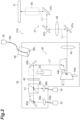
- FIG 2 is a diagram illustrating a configuration in a state in which switching to the first inspection system is performed, and a first optical path in the optical device 31A
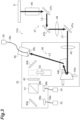
- FIG. 3 is a diagram illustrating a configuration in a state in which switching to the second inspection system is performed, and a second optical path in the optical device 31A.
- the optical device 31A includes a casing 32, a light source (a first light source) 33, a photodetector (a first photodetector) 34, a photodetector (a second photodetector) 35, an internal optical system 36 disposed inside the casing 32, and an external optical system 37 disposed outside the casing 32.
- the light source 33 is operated by a power supply (not illustrated) and generates and emits light for irradiating the semiconductor device D with for generating a pattern image of the semiconductor device D.
- the light source 33 is, for example, an incoherent light source such as a light emitting diode (LED) or a super luminescent diode (SLD) light source.
- the light source 33 may be, for example, a coherent light source such as a laser.
- the light output from the light source 33 is radiated to the semiconductor device D via the internal optical system 36 and the external optical system 37.
- the photodetector 34 detects the reflected light from the semiconductor device D, and outputs a detection signal of the reflected light of the semiconductor device D to the calculator 21.
- the photodetector 34 is a light reception element such as a photomultiplier tube, a photodiode (PD), or an avalanche photodiode (APD).
- the reflected light from the semiconductor device D is incident on the photodetector 34 via the external optical system 37 and the internal optical system 36.
- the photodetector 35 detects emitted light generated in the semiconductor device D, and outputs a detection signal of the emitted light of the semiconductor device D to the calculator 21.
- the photodetector 35 is, for example, a superconducting single photon detector (SSPD) that is a superconducting single photon detector, a photomultiplier tube, or a silicon photomultiplier (SiPM).
- SSPD superconducting single photon detector
- SiPM silicon photomultiplier
- the internal optical system 36 includes optical fibers 38a, 38b, and 38c, collimator lenses 39a, 39b, and 39c, a mirror 40a, a light guide element (mirror) 40b, a polarization beam splitter (hereinafter referred to as "PBS") 41, a 1/4 wavelength plate 42, a variable pupil 43, a pair of Galvano mirrors 44a and 44b, and a pupil relay lens 45.
- PBS polarization beam splitter
- One ends of the optical fibers 38a, 38b, and 38c are respectively optically connected to the light source 33, the photodetector 34, and the photodetector 35 outside the casing 32, and the other ends of the optical fibers 38a, 38b, and 38c are respectively optically connected to the collimator lenses 39a, 39b, and 39c inside the casing 32.
- the collimator lens 39a converts the light radiated from the light source 33 into parallel light
- the collimator lenses 39b and 39c convert light incident on the photodetector 34 and the photodetector 35 into parallel light.
- the mirror 40a is disposed on the light output side of the collimator lens 39a inside the casing 32, the PBS 41 is disposed on the light input side of the collimator lens 39b, and the mirror 40a, the PBS 41, the 1/4 wavelength plate 42, the variable pupil 43, and a mirror 40b are arranged side by side in line in that order.
- the mirror 40a reflects the light output from the light source 33 toward the PBS 41.
- the PBS 41 transmits linearly polarized light in the light output from the light source 33 toward the mirror 40b, and the 1/4 wavelength plate 42 converts the linearly polarized light into circularly polarized light and outputs the circularly polarized light toward the mirror 40b.
- the 1/4 wavelength plate 42 converts reflected light from the semiconductor device D incident from the mirror 40b side into linearly polarized light having a polarization direction orthogonal to that of the linearly polarized light of the light output from the light source 33, and the PBS 41 reflects the linearly polarized light of the reflected light toward the photodetector 34.
- the variable pupil 43 is provided on an optical path between the mirror 40a and the mirror 40b to be movable into and out of the optical path and is intended to change a size of the pupil.
- the mirror 40b is optically connected to the light source 33 and the photodetector 34 as described above. Specifically, the mirror 40b reflects the light output from the light source 33 and guides the light toward the pair of Galvano mirrors 44a and 44b, which are light scanning units. Further, the mirror 40b receives the reflected light from the semiconductor device D via the pair of Galvano mirrors 44a and 44b, and causes the reflected light to be incident on the photodetector 34 via the variable pupil 43, the 1/4 wavelength plate 42, the PBS 41, the collimator lens 39b, and the optical fiber 38b.
- the mirror is used as the light guide element in the embodiment, an optical fiber or the like may be used as long as the optical fiber or the like is an optical element capable of guiding light between the light source 33 and/or the photodetector 34 and the pair of Galvano mirrors 44a and 44b.
- the pair of Galvano mirrors 44a and 44b are configured to be optically connectable to the light source 33 and the photodetector 34 via the mirror 40b, and are optically connected to the external optical system 37 via the pupil relay lens 45. That is, the pair of Galvano mirrors 44a and 44b are light scanning units that are disposed in a reflection direction of the light from the light source 33, of the mirror 40b, and can reflect the light while performing two-dimensional scanning with the light, and have a configuration in which two Galvano mirrors of which a deflection angle can be changed around on a predetermined axis are combined. The pair of Galvano mirrors 44a and 44b can two-dimensionally scan the semiconductor device D with the light to be radiated to the semiconductor device D.
- the pair of Galvano mirrors 44a and 44b can also guide the reflected light or emitted light at a predetermined point of the semiconductor device D toward a predetermined position of the mirror 40b or the collimator lens 39c while performing two-dimensional position selection.
- the semiconductor device D may be two-dimensionally illuminated by reflecting a separately prepared light source by one of the mirrors in a state in which the pair of Galvano mirrors 44a and 44b are stopped.
- the deflection angle of the pair of Galvano mirrors 44a and 44b is configured to be able to be controlled by the control unit 21a of the calculator 21.
- the collimator lens 39c is held inside the casing 32 by an attachment portion (a first attachment portion) 46 provided at a position on the casing 32 at which the collimator lens 39c can be optically connected to the pair of Galvano mirrors 44a and 44b.
- this attachment portion 46 forms a cylindrical member, and is a portion for attaching an optical element such as a collimator lens inside the casing 32.
- the other end of the optical fiber 38c is optically connected to the collimator lens 39c inside the attachment portion 46.
- the external optical system 37 includes mirrors 47a, 47b and 47c, a pupil relay lens 48, and an objective lens unit 49.
- the external optical system 37 guides the light from the light source 33 to be incident on the semiconductor device D, and guides the reflected light and the emitted light generated in the semiconductor device D to be incident on the internal optical system 36. That is, the light from the light source 33 incident from the internal optical system 36 is reflected by the mirror 47a, transmitted through the pupil relay lens 48, sequentially reflected by the mirrors 47b and 47c, and then radiated to the semiconductor device D through the objective lens unit 49.
- the reflected light or the emitted light in the semiconductor device D passes through the objective lens unit 49, and is sequentially reflected by the mirrors 47c and 47b, transmitted through the pupil relay lens 48, and then reflected by the mirror 47a, such that the light is incident on the internal optical system 36.
- the objective lens unit 49 may include a plurality of objective lenses with different magnifications and may be configured so that the objective lenses are switched by a turret.
- the optical device 31A configured as described above is configured to be able to perform control so that the optical path for optical connection to the semiconductor device D is switched by the calculator 21. That is, the calculator 21 includes the control unit 21a as a functional component.
- the control unit 21a of the calculator 21 controls the deflection angle of the pair of Galvano mirrors 44a and 44b so that the optical path optically connected to the semiconductor device D is switched between the first optical path L1 ( FIG. 2 ) including the external optical system 37 and the internal optical system 36 via the pair of Galvano mirrors 44a and 44b and the mirror 40b, and the second optical path L2 ( FIG. 3 ) including the external optical system 37 and the internal optical system 36 via the pair of Galvano mirrors 44a and 44b and the collimator lens 39c in the attachment portion 46 by controlling the deflection angle of the pair of Galvano mirrors 44a and 44b.
- control unit 21a switches the optical path to the first optical path L1 when the user has instructed execution of the inspection of the reflected light via the input unit 23, and switches the optical path to the second optical path L2 when the user has instructed execution of the inspection of the emitted light via the input unit 23.
- control unit 21a performs control so that the semiconductor device D is two-dimensionally scanned with the light to be radiated to the semiconductor device D by sequentially changing the deflection angle of the pair of Galvano mirrors 44a and 44b within a predetermined angle range, and performs control so that a position of the reflected light or the emitted light is selected at a predetermined point of the semiconductor device D, and the position-selected light is guided, by two-dimensional scanning.
- FIG. 4 illustrates an example of a change range of the deflection angle of the pair of Galvano mirrors 44a and 44b controlled by the control unit 21a of the calculator 21.
- a horizontal axis H indicates the deflection angle in one direction of the pair of Galvano mirrors 44a and 44b controlled by the control unit 21a
- a vertical axis V indicates the deflection angle in the other direction perpendicular to the one direction of the pair of Galvano mirrors 44a and 44b controlled by the control unit 21a.
- the one direction is a horizontal direction
- the other direction is a vertical direction.
- the control unit 21a performs control so that the range W1 of the deflection angle when switching to the first optical path L1 has been performed and the range W2 of the deflection angle when switching to the second optical path L2 has been performed do not overlap.
- the calculator 21 also has a function of generating a pattern image or an emitted light image (an analysis image) on the basis of detection signals input from the photodetectors 34 and 35. That is, the calculator 21 generates a pattern image indicating intensity of the reflected light at each two-dimensional position of the semiconductor device D on the basis of a detection signal obtained while scanning the semiconductor device D with the light from the light source 33 under the control of the control unit 21a. Similarly, the calculator 21 generates an emitted light image indicating intensity of the emitted light at each two-dimensional position of the semiconductor device D on the basis of a detection signal obtained while scanning an observation position on the semiconductor device D under the control of the control unit 21a. Further, the calculator 21 generates, as the analysis image, a superimposed image in which the pattern image and the emitted light image are superimposed, and outputs the generated analysis image to the display unit 22.
- the deflection angle of the pair of Galvano mirrors 44a and 44b is controlled so that the optical path optically connected to the semiconductor device D is switched between the first optical path L1 and the second optical path L2. Accordingly, measurement of the reflected light of the semiconductor device D using the light source 33, the photodetector 34, and the mirror 40b, and inspection of the emitted light of the semiconductor device D using the photodetector 35 attached to the attachment portion 46 can be executed in a switching manner.
- the optical system of each measurement system can be set to an optimal state independently, and as a result, spatial accuracy of the optical path in each inspection system can be improved, and as a result, the semiconductor device D can be inspected with high accuracy.
- the photodetector 35 is attached to the attachment portion 46 such that the emitted light of the semiconductor device D can be detected via the second optical path L2.
- the attachment portion 46 it is possible to easily replace the photodetector 35 with another optical element and to perform optimal inspection.
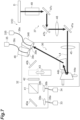
- the optical device 31B further includes the light source (a third light source) 133 that radiates laser light for performing marking indicating a fault location.
- This light source 133 is optically connected to an internal optical system 36 via a collimator lens 39d and an optical fiber 38d held by an attachment portion (a third attachment portion) 146 provided at a position on a casing 32 at which optical connection to a pair of Galvano mirrors 44a and 44b is possible.
- the attachment portion 146 forms a cylindrical member, and is a portion for attaching an optical element such as a collimator lens inside the casing 32 on an extended line connecting the pair of Galvano mirrors 44a and 44b to a dichroic mirror 140b.
- fault analysis of the semiconductor device D may be performed by using, as the light source 133, a laser light source that outputs laser light having a wavelength of 1064 nm, which has energy lower than a band gap of silicon, or laser light having a wavelength of 1300 nm, which has energy higher than the band gap of the silicon.
- a laser light source that outputs laser light having a wavelength of 1064 nm, which has energy lower than a band gap of silicon, or laser light having a wavelength of 1300 nm, which has energy higher than the band gap of the silicon.
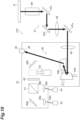
- the optical device 3 1D further includes a photodetector 335 for inspecting emitted light of the semiconductor device D.
- This photodetector 335 is optically connected to an internal optical system 36 via a collimator lens 39e and an optical fiber 38e held by an attachment portion (a second attachment portion) 346 provided at a position on a casing 32 at which the photodetector 335 can be optically connected to a pair of Galvano mirrors 44a and 44b.
- the attachment portion 346 forms a cylindrical member, and is a portion for attaching an optical element such as a collimator lens inside the casing 32.
- the control unit 21a of the calculator 21 controls the deflection angle of the pair of Galvano mirrors 44a and 44b so that the optical path optically connected to the semiconductor device D is switched to the third optical path L4 including the external optical system 37 and the internal optical system 36 via the pair of Galvano mirrors 44a and 44b and the collimator lens 39e in the attachment portion 346.
- the control unit 21a switches the optical path to the optical path L4.
- control unit 21a performs control so that the range W1 of the deflection angle when switching to the first optical path L1 has been performed, the range W2 of the deflection angle when switching to the second optical path L2 has been performed, and the range W4 of the deflection angle when switching to the third optical path L4 has been performed do not overlap.
- the optical system of each measurement system can be set to an optimal state independently, and as a result, spatial accuracy of the optical path in each inspection system can be improved. As a result, the semiconductor device D can be inspected with high accuracy.
- a light source 333 for illumination, marking, heating, or generation of a photovoltaic current of the semiconductor device D may be attached to the attachment portion 346 instead of the photodetector 335, as illustrated in FIG. 9 .
- the photodetector 35 is optically connected to the Galvano mirrors 44a and 44b via the collimator lens and the optical fiber in the first embodiment, the photodetector 35 may be optically directly connected to the Galvano mirrors 44a and 44b, as in an optical device 31F according to a modification example illustrated in FIG. 10 .
- an optical path division element 50 to which a light source 233 and a photodetector 334 have been optically connected may be attached to the attachment portion 46, as in an optical device 31H according to a modification example illustrated in FIG. 12 .
- the light source 233 is, for example, an incoherent light source such as a light emitting diode (LED) or a super luminescent diode (SLD) light source, or a coherent light source such as a laser.
- the photodetector 334 is, for example, a light reception element such as a photomultiplier tube, a photodiode (PD), or an avalanche photodiode (APD).
- the optical path division element 50 is, for example, an optical circulator.
- the semiconductor device D when the semiconductor device D is irradiated with the light from the light source 233 via a second optical path L5, light reflected and returning via the second optical path L5 can be guided to the photodetector 334 and detected.
- a 1/2 wavelength plate may be disposed on the optical path L5 as the polarization element 51 and rotated to any angle so that the semiconductor device D is irradiated with light including any linearly polarized light.
- a polarization maintaining optical fiber coupler may be used as the optical path division element 50, and a 1/4 wavelength plate may be disposed on the optical path L5 as the polarization element 51.
- the semiconductor device D can be irradiated with the light output from the light source 233 as circularly polarized light, and the light reflected and caused to return by the semiconductor device D can be guided to the photodetector 334 and detected.
- the reflected light of the light radiated from the light source 233 to the semiconductor device D can be detected by the photodetector 334 so that the pattern image is generated, or light having different wavelengths can be generated by the light source 33 and the light source 133 and radiated to the semiconductor device D via the first optical path L6 so that default analysis can be performed.
- the semiconductor inspection device may further include the first photodetector configured to detect the light from the semiconductor device, and the light guide element may be optically connected to the first photodetector. In this case, switching between measurement of the light of the semiconductor device using the first light source, the first photodetector, and the light guide element, and inspection of the semiconductor device using the optical element attached to the first attachment portion can be performed and the measurement and the inspection can be executed.
- the second photodetector configured to detect the light from the semiconductor device may be further included, and the second photodetector may be attached to the first attachment portion such that the light can be detected via the second optical path.
- the optical path optically connected to the semiconductor device is switched to the second optical path, the light from the semiconductor device can be measured using the second photodetector.
- the second photodetector may be attached to the first attachment portion via the collimator lens and the optical fiber.
- the optical path optically connected to the semiconductor device is switched to the second optical path, the light from the semiconductor device can be measured by the second photodetector via the collimator lens and the optical fiber.
- the second light source may be attached to the first attachment portion via the collimator lens and the optical fiber.
- the semiconductor device when the optical path optically connected to the semiconductor device is switched to the second optical path, the semiconductor device can be irradiated with light using the second light source via the collimator lens and the optical fiber and can be inspected.
- a second light source configured to emit light for irradiating the semiconductor device with, a second photodetector configured to detect light from the semiconductor device, and an optical path division element optically connected to the second light source and the second photodetector may be further included, and the optical path division element may be attached to the first attachment portion, such that the light can be radiated and/or detected via the second optical path.
- the optical path optically connected to the semiconductor device is switched to the second optical path, it is possible to measure the light from the semiconductor device while irradiating the semiconductor device with the light using the second light source.
- the casing may further include a second attachment portion for attaching an optical element, the second attachment portion being provided at a position at which the optical element can be optically connected to the pair of Galvano mirrors, and the control unit may control the deflection angle so that switching among the first optical path, the second optical path, and the third optical path passing through the pair of Galvano mirrors and the second attachment portion is performed, and may control the deflection angle so that the deflection angle when switching to the first optical path has been performed, the deflection angle when switching to the second optical path has been performed, and the deflection angle when switching to the third optical path has been performed do not overlap.
- the optical path optically connected to the semiconductor device by switching the optical path optically connected to the semiconductor device to the third optical path, it is possible to execute the inspection of the semiconductor device using the optical element attached to the second attachment portion in a switching manner.
- the control since the control is performed so that the deflection angle of the Galvano mirror when switching to the first optical path has been performed, the deflection angle of the Galvano mirror when switching to the second optical path has been performed, and the deflection angle of the Galvano mirror when switching to the third optical path has been performed do not overlap, the optical system of each inspection system can be set to an optimal state independently, and as a result, spatial accuracy of the optical path in each inspection system can be improved. As a result, it is possible to inspect the semiconductor device with high accuracy.
- the light guide element may be a mirror.
- the mirror as the light guide element may be a dichroic mirror, and the casing may further include the third attachment portion for attaching the optical element on an extended line connecting the pair of Galvano mirrors to the dichroic mirror. In this case, when the optical path optically connected to the semiconductor device is switched to the first optical path, inspection of the semiconductor device using the optical element attached to the third attachment portion can be performed.
- a third light source optically connected to the light guide element may be further included.
- the optical path optically connected to the semiconductor device is switched to the first optical path, it is possible to perform the measurement of the light of the semiconductor device while irradiating the semiconductor device with light using the third light source.
- the second photodetector may be a superconducting single photon detector.
- the semiconductor inspection device is used as an application, it is possible to inspect a semiconductor device with high accuracy by improving spatial accuracy of optical paths in a plurality of optical elements.
Landscapes
- Physics & Mathematics (AREA)
- General Physics & Mathematics (AREA)
- Engineering & Computer Science (AREA)
- Health & Medical Sciences (AREA)
- Optics & Photonics (AREA)
- Life Sciences & Earth Sciences (AREA)
- Chemical & Material Sciences (AREA)
- Analytical Chemistry (AREA)
- Biochemistry (AREA)
- General Health & Medical Sciences (AREA)
- Immunology (AREA)
- Pathology (AREA)
- Computer Vision & Pattern Recognition (AREA)
- Electromagnetism (AREA)
- Toxicology (AREA)
- Quality & Reliability (AREA)
- Theoretical Computer Science (AREA)
- General Engineering & Computer Science (AREA)
- Signal Processing (AREA)
- Investigating Materials By The Use Of Optical Means Adapted For Particular Applications (AREA)
- Tests Of Electronic Circuits (AREA)
- Testing Or Measuring Of Semiconductors Or The Like (AREA)
- Mechanical Light Control Or Optical Switches (AREA)
- Crystals, And After-Treatments Of Crystals (AREA)
- Led Devices (AREA)
Claims (12)
- Dispositif d'inspection de semi-conducteur pour inspecter un dispositif à semi-conducteur (D), le dispositif d'inspection de semi-conducteur comprenant :une première source (33) de lumière configurée pour émettre de la lumière pour irradier le dispositif à semi-conducteur avec ;un élément (40b) de guidage de lumière optiquement connecté à la première source (33) de lumière ;une paire de miroirs Galvano (44a, 44b) disposés à des positions au niveau desquelles les miroirs Galvano (44a, 44b) peuvent être optiquement connectés à la première source (33) de lumière via l'élément (40b) de guidage de lumière ;un boîtier (32) renfermant l'élément (40b) de guidage de lumière et la paire de miroirs Galvano (44a, 44b) en son sein et incluant une première partie de fixation (46) pour fixer un élément optique, la première partie de fixation (46) étant disposée à une position au niveau de laquelle l'élément optique peut être optiquement connecté à la paire de miroirs Galvano (44a, 44b) ; etune unité de commande (21a) configurée pour commander un angle de déviation de la paire de miroirs Galvano (44a, 44b),dans lequel l'unité de commande (21a) est configurée pourcommander l'angle de déviation de sorte qu'un chemin optique optiquement connecté au dispositif à semi-conducteur est commuté entre un premier chemin optique (L1) passant à travers la paire de miroirs Galvano (44a, 44b) et l'élément (40b) de guidage de lumière et un deuxième chemin optique passant à travers la paire de miroirs Galvano (44a, 44b) et la première partie de fixation (46), et pourcommander l'angle de déviation de sorte que l'angle de déviation lorsqu'une commutation vers le premier chemin optique (L1) a été mise en oeuvre et l'angle de déviation lorsqu'une commutation vers le deuxième chemin optique a été mise en oeuvre ne se chevauchent pas.
- Dispositif d'inspection de semi-conducteur selon la revendication 1, comprenant en outre :un premier photodétecteur (34) configuré pour détecter de la lumière provenant du dispositif à semi-conducteur (D),dans lequel l'élément (40b) de guidage de lumière est optiquement connecté au premier photodétecteur (34).
- Dispositif d'inspection de semi-conducteur selon la revendication 1 ou la revendication 2, comprenant en outre :un deuxième photodétecteur (35) configuré pour détecter de la lumière provenant du dispositif à semi-conducteur (D),dans lequel le deuxième photodétecteur (35) est configuré pour détecter la lumière via le deuxième chemin optique en étant fixé à la première partie de fixation (46).
- Dispositif d'inspection de semi-conducteur selon la revendication 3, dans lequel le deuxième photodétecteur (35) est fixé à la première partie de fixation (46) via une lentille de collimation (39a à 39e) et une fibre optique (38a à 38e).
- Dispositif d'inspection de semi-conducteur selon la revendication 1 ou la revendication 2, comprenant en outre :une deuxième source (333) de lumière configurée pour émettre de la lumière pour irradier le dispositif à semi-conducteur (D) avec,dans lequel la deuxième source (333) de lumière est fixée à la première partie de fixation (46), de sorte que la lumière peut être irradiée via le deuxième chemin optique.
- Dispositif d'inspection de semi-conducteur selon la revendication 5, dans lequel la deuxième source (333) de lumière est fixée à la première partie de fixation (46) via une lentille de collimation (39a à 39e) et une fibre optique (38a à 38e).
- Dispositif d'inspection de semi-conducteur selon la revendication 1 ou la revendication 2, comprenant en outre :une deuxième source (333) de lumière configurée pour émettre de la lumière pour irradier le dispositif à semi-conducteur (D) avec, un deuxième photodétecteur (35) configuré pour détecter de la lumière provenant du dispositif à semi-conducteur (D), et un élément (50) de division de chemin optique optiquement connecté à la deuxième source (333) de lumière et au deuxième photodétecteur (35),dans lequel l'élément (50) de division de chemin optique est fixé à la première partie de fixation (46), de sorte que la lumière peut être irradiée et/ou détectée via le deuxième chemin optique (L2).
- Dispositif d'inspection de semi-conducteur selon l'une quelconque des revendications 1 à 7,dans lequel le boîtier (32) inclut en outre une deuxième partie de fixation (346) pour fixer un élément optique, la deuxième partie de fixation (346) étant disposée à une position au niveau de laquelle l'élément optique peut être optiquement connecté à la paire de miroirs Galvano (44a, 44b),l'unité de commande (21a) est configurée pourcommander l'angle de déviation de sorte qu'une commutation entre le premier chemin optique (L1), le deuxième chemin optique (L2) et un troisième chemin optique (L4) passant à travers la paire de miroirs Galvano (44a, 44b) et la deuxième partie de fixation (346) est mise en oeuvre, et pourcommander l'angle de déviation de sorte que l'angle de déviation lorsqu'une commutation vers le premier chemin optique (L1) a été mise en oeuvre, l'angle de déviation lorsqu'une commutation vers le deuxième chemin optique (L2) a été mise en oeuvre, et l'angle de déviation lorsqu'une commutation vers le troisième chemin optique (L4) a été mise en oeuvre ne se chevauchent pas.
- Dispositif d'inspection de semi-conducteur selon l'une quelconque des revendications 1 à 8, dans lequel l'élément (40b) de guidage de lumière est un miroir.
- Dispositif d'inspection de semi-conducteur selon la revendication 9,dans lequel le miroir (40b) est un miroir dichroïque, etle boîtier (32) inclut en outre une troisième partie de fixation (146) pour fixer un élément optique sur une ligne étendue connectant la paire de miroirs Galvano (44a, 44b) au miroir dichroïque (40b).
- Dispositif d'inspection de semi-conducteur selon l'une quelconque des revendications 1 à 10, comprenant en outre :
une troisième source (133) de lumière optiquement connectée à l'élément (40b) de guidage de lumière. - Dispositif d'inspection de semi-conducteur selon la revendication 3, dans lequel le deuxième photodétecteur (35) est un détecteur de photon unique supraconducteur.
Priority Applications (1)
| Application Number | Priority Date | Filing Date | Title |
|---|---|---|---|
| EP24184687.2A EP4414694B1 (fr) | 2017-06-02 | 2018-03-07 | Dispositif d'inspection de semi-conducteur |
Applications Claiming Priority (2)
| Application Number | Priority Date | Filing Date | Title |
|---|---|---|---|
| JP2017109918A JP6419893B1 (ja) | 2017-06-02 | 2017-06-02 | 半導体検査装置 |
| PCT/JP2018/008830 WO2018220931A1 (fr) | 2017-06-02 | 2018-03-07 | Dispositif d'inspection de semi-conducteur |
Related Child Applications (2)
| Application Number | Title | Priority Date | Filing Date |
|---|---|---|---|
| EP24184687.2A Division EP4414694B1 (fr) | 2017-06-02 | 2018-03-07 | Dispositif d'inspection de semi-conducteur |
| EP24184687.2A Division-Into EP4414694B1 (fr) | 2017-06-02 | 2018-03-07 | Dispositif d'inspection de semi-conducteur |
Publications (4)
| Publication Number | Publication Date |
|---|---|
| EP3633355A1 EP3633355A1 (fr) | 2020-04-08 |
| EP3633355A4 EP3633355A4 (fr) | 2021-03-31 |
| EP3633355B1 true EP3633355B1 (fr) | 2024-08-07 |
| EP3633355C0 EP3633355C0 (fr) | 2024-08-07 |
Family
ID=64098718
Family Applications (2)
| Application Number | Title | Priority Date | Filing Date |
|---|---|---|---|
| EP24184687.2A Active EP4414694B1 (fr) | 2017-06-02 | 2018-03-07 | Dispositif d'inspection de semi-conducteur |
| EP18808722.5A Active EP3633355B1 (fr) | 2017-06-02 | 2018-03-07 | Dispositif d'inspection de semi-conducteur |
Family Applications Before (1)
| Application Number | Title | Priority Date | Filing Date |
|---|---|---|---|
| EP24184687.2A Active EP4414694B1 (fr) | 2017-06-02 | 2018-03-07 | Dispositif d'inspection de semi-conducteur |
Country Status (8)
| Country | Link |
|---|---|
| US (2) | US11209476B2 (fr) |
| EP (2) | EP4414694B1 (fr) |
| JP (1) | JP6419893B1 (fr) |
| KR (2) | KR102459819B1 (fr) |
| CN (2) | CN115326827B (fr) |
| SG (1) | SG11201909742XA (fr) |
| TW (2) | TWI831288B (fr) |
| WO (1) | WO2018220931A1 (fr) |
Families Citing this family (10)
| Publication number | Priority date | Publication date | Assignee | Title |
|---|---|---|---|---|
| JP6820184B2 (ja) * | 2016-10-26 | 2021-01-27 | 浜松ホトニクス株式会社 | 半導体デバイス検査方法及び半導体デバイス検査装置 |
| US11536792B2 (en) * | 2020-04-30 | 2022-12-27 | Applied Materials Israel Ltd. | Test of an examination tool |
| KR102918469B1 (ko) | 2020-05-26 | 2026-01-28 | 하마마츠 포토닉스 가부시키가이샤 | 반도체 디바이스 검사 방법 및 반도체 디바이스 검사 장치 |
| US12517170B2 (en) | 2020-05-26 | 2026-01-06 | Hamamatsu Photonics K.K. | Semiconductor device inspection method and semiconductor device inspection device |
| WO2022064798A1 (fr) * | 2020-09-23 | 2022-03-31 | 浜松ホトニクス株式会社 | Dispositif d'inspection |
| JP7306355B2 (ja) * | 2020-09-23 | 2023-07-11 | トヨタ自動車株式会社 | 変換アダプタ |
| CN112485271B (zh) * | 2020-12-04 | 2024-07-05 | 中山市东照照明有限公司 | 一种pcb板检测装置 |
| WO2023002688A1 (fr) * | 2021-07-19 | 2023-01-26 | 浜松ホトニクス株式会社 | Dispositif d'analyse d'erreur de semi-conducteur et procédé d'analyse d'erreur de semi-conducteur |
| WO2026061792A1 (fr) * | 2024-09-17 | 2026-03-26 | Norlase Aps | Système d'ophtalmoscope indirect laser (oil) multi-spots pouvant être monté sur le corps |
| CN120846649B (zh) * | 2025-09-22 | 2025-12-30 | 晋城市光机电产业协调服务中心(晋城市光机电产业研究院) | 一种半导体激光器综合性能测试系统 |
Family Cites Families (24)
| Publication number | Priority date | Publication date | Assignee | Title |
|---|---|---|---|---|
| JPH0580497A (ja) * | 1991-09-20 | 1993-04-02 | Canon Inc | 面状態検査装置 |
| JPH05129399A (ja) * | 1991-11-01 | 1993-05-25 | Toshiba Corp | 表面付着粒子検出装置 |
| JP3798481B2 (ja) * | 1996-10-16 | 2006-07-19 | 株式会社キーエンス | レーザマーキング装置 |
| JPH11197109A (ja) * | 1998-01-19 | 1999-07-27 | Kowa Co | 走査型レーザー検眼鏡 |
| CN1129788C (zh) * | 1998-08-10 | 2003-12-03 | 三菱电机株式会社 | 印刷电路基板的检查装置 |
| JP2002353558A (ja) * | 2001-05-25 | 2002-12-06 | Opnext Japan Inc | 半導体レーザモジュール及びこれを用いた光ファイバ通信機器 |
| JP5110894B2 (ja) * | 2007-02-05 | 2012-12-26 | 株式会社ジャパンディスプレイウェスト | 欠陥修正装置、配線基板の製造方法、ディスプレイ装置の製造方法 |
| EP2169442B1 (fr) * | 2007-07-19 | 2015-10-28 | Nikon Corporation | Microscope confocal de type à balayage |
| US7952374B2 (en) | 2008-06-02 | 2011-05-31 | Quantum Focus Instruments Corporation | Transient emission scanning microscopy |
| JP2009295414A (ja) | 2008-06-05 | 2009-12-17 | Panasonic Corp | 誘導加熱調理器 |
| JP5187843B2 (ja) * | 2008-09-01 | 2013-04-24 | 浜松ホトニクス株式会社 | 半導体検査装置及び検査方法 |
| JP5231927B2 (ja) * | 2008-10-06 | 2013-07-10 | 株式会社日立ハイテクノロジーズ | 微小突起物検査装置 |
| JP2011075441A (ja) * | 2009-09-30 | 2011-04-14 | Hamamatsu Photonics Kk | 半導体デバイス故障解析装置 |
| JP2012083351A (ja) * | 2011-10-17 | 2012-04-26 | Hitachi High-Technologies Corp | 欠陥検査装置およびその方法 |
| US8836934B1 (en) * | 2012-05-15 | 2014-09-16 | The Boeing Company | Contamination identification system |
| US10520721B2 (en) * | 2013-03-15 | 2019-12-31 | The Brain Window, Inc. | Optical beam scanning system having a synthetic center of beam rotation |
| CN204054955U (zh) * | 2014-05-08 | 2014-12-31 | 佛山市联动科技实业有限公司 | 带检测的激光打标机 |
| KR102242559B1 (ko) * | 2014-12-01 | 2021-04-20 | 삼성전자주식회사 | 광학 검사 장치 |
| JP6534854B2 (ja) * | 2015-04-27 | 2019-06-26 | オリンパス株式会社 | レーザ走査型顕微鏡 |
| CN106405826B (zh) * | 2015-07-29 | 2019-04-19 | 大族激光科技产业集团股份有限公司 | 一种双光路成像的振镜扫描系统及扫描方法 |
| JP2017129650A (ja) * | 2016-01-19 | 2017-07-27 | 株式会社ディスコ | 走査用ミラー |
| US10841548B2 (en) * | 2016-03-01 | 2020-11-17 | Funai Electric Co., Ltd. | Oscillating mirror element and projector |
| US10324185B2 (en) * | 2017-11-22 | 2019-06-18 | Luminar Technologies, Inc. | Reducing audio noise in a lidar scanner with a polygon mirror |
| US10578720B2 (en) * | 2018-04-05 | 2020-03-03 | Luminar Technologies, Inc. | Lidar system with a polygon mirror and a noise-reducing feature |
-
2017
- 2017-06-02 JP JP2017109918A patent/JP6419893B1/ja active Active
-
2018
- 2018-03-07 CN CN202210947735.XA patent/CN115326827B/zh active Active
- 2018-03-07 US US16/617,840 patent/US11209476B2/en active Active
- 2018-03-07 CN CN201880035932.6A patent/CN110691968B/zh active Active
- 2018-03-07 WO PCT/JP2018/008830 patent/WO2018220931A1/fr not_active Ceased
- 2018-03-07 SG SG11201909742X patent/SG11201909742XA/en unknown
- 2018-03-07 KR KR1020197030977A patent/KR102459819B1/ko active Active
- 2018-03-07 EP EP24184687.2A patent/EP4414694B1/fr active Active
- 2018-03-07 KR KR1020227036977A patent/KR102562196B1/ko active Active
- 2018-03-07 EP EP18808722.5A patent/EP3633355B1/fr active Active
- 2018-03-15 TW TW111126174A patent/TWI831288B/zh active
- 2018-03-15 TW TW107108860A patent/TWI769229B/zh active
-
2021
- 2021-10-29 US US17/515,145 patent/US11714120B2/en active Active
Also Published As
| Publication number | Publication date |
|---|---|
| EP4414694B1 (fr) | 2026-08-05 |
| JP2018205083A (ja) | 2018-12-27 |
| KR102459819B1 (ko) | 2022-10-27 |
| EP4414694A2 (fr) | 2024-08-14 |
| TW202242395A (zh) | 2022-11-01 |
| CN110691968B (zh) | 2022-08-26 |
| JP6419893B1 (ja) | 2018-11-07 |
| US11209476B2 (en) | 2021-12-28 |
| CN115326827B (zh) | 2025-05-02 |
| CN110691968A (zh) | 2020-01-14 |
| KR20220150993A (ko) | 2022-11-11 |
| EP3633355C0 (fr) | 2024-08-07 |
| EP3633355A1 (fr) | 2020-04-08 |
| US20200110129A1 (en) | 2020-04-09 |
| US20220050137A1 (en) | 2022-02-17 |
| SG11201909742XA (en) | 2019-11-28 |
| US11714120B2 (en) | 2023-08-01 |
| EP3633355A4 (fr) | 2021-03-31 |
| TW201903394A (zh) | 2019-01-16 |
| CN115326827A (zh) | 2022-11-11 |
| TWI769229B (zh) | 2022-07-01 |
| TWI831288B (zh) | 2024-02-01 |
| KR20200013639A (ko) | 2020-02-07 |
| WO2018220931A1 (fr) | 2018-12-06 |
| KR102562196B1 (ko) | 2023-08-02 |
| EP4414694A3 (fr) | 2024-11-13 |
Similar Documents
| Publication | Publication Date | Title |
|---|---|---|
| US11714120B2 (en) | Semiconductor inspection device | |
| US11402200B2 (en) | Measuring device, observing device and measuring method | |
| EP3754693B1 (fr) | Procédé et dispositif de mesure de durée de vie de porteuse | |
| US11967061B2 (en) | Semiconductor apparatus examination method and semiconductor apparatus examination apparatus | |
| US20200132629A1 (en) | Inspection device and inspection method | |
| WO2015186711A1 (fr) | Dispositif d'inspection et procédé pour disposer un cristal magnéto-optique | |
| US11906571B2 (en) | Optical detection system and laser light providing module without using an optical fiber | |
| JP6909195B2 (ja) | 半導体検査装置 | |
| US20210333207A1 (en) | Optical measurement device | |
| US9417281B1 (en) | Adjustable split-beam optical probing (ASOP) |
Legal Events
| Date | Code | Title | Description |
|---|---|---|---|
| STAA | Information on the status of an ep patent application or granted ep patent |
Free format text: STATUS: THE INTERNATIONAL PUBLICATION HAS BEEN MADE |
|
| PUAI | Public reference made under article 153(3) epc to a published international application that has entered the european phase |
Free format text: ORIGINAL CODE: 0009012 |
|
| STAA | Information on the status of an ep patent application or granted ep patent |
Free format text: STATUS: REQUEST FOR EXAMINATION WAS MADE |
|
| 17P | Request for examination filed |
Effective date: 20191105 |
|
| AK | Designated contracting states |
Kind code of ref document: A1 Designated state(s): AL AT BE BG CH CY CZ DE DK EE ES FI FR GB GR HR HU IE IS IT LI LT LU LV MC MK MT NL NO PL PT RO RS SE SI SK SM TR |
|
| AX | Request for extension of the european patent |
Extension state: BA ME |
|
| DAV | Request for validation of the european patent (deleted) | ||
| DAX | Request for extension of the european patent (deleted) | ||
| A4 | Supplementary search report drawn up and despatched |
Effective date: 20210302 |
|
| RIC1 | Information provided on ipc code assigned before grant |
Ipc: G01N 21/88 20060101ALI20210224BHEP Ipc: G01N 21/956 20060101AFI20210224BHEP Ipc: G01R 31/302 20060101ALI20210224BHEP |
|
| STAA | Information on the status of an ep patent application or granted ep patent |
Free format text: STATUS: EXAMINATION IS IN PROGRESS |
|
| 17Q | First examination report despatched |
Effective date: 20221110 |
|
| GRAP | Despatch of communication of intention to grant a patent |
Free format text: ORIGINAL CODE: EPIDOSNIGR1 |
|
| STAA | Information on the status of an ep patent application or granted ep patent |
Free format text: STATUS: GRANT OF PATENT IS INTENDED |
|
| INTG | Intention to grant announced |
Effective date: 20240315 |
|
| GRAS | Grant fee paid |
Free format text: ORIGINAL CODE: EPIDOSNIGR3 |
|
| GRAA | (expected) grant |
Free format text: ORIGINAL CODE: 0009210 |
|
| STAA | Information on the status of an ep patent application or granted ep patent |
Free format text: STATUS: THE PATENT HAS BEEN GRANTED |
|
| AK | Designated contracting states |
Kind code of ref document: B1 Designated state(s): AL AT BE BG CH CY CZ DE DK EE ES FI FR GB GR HR HU IE IS IT LI LT LU LV MC MK MT NL NO PL PT RO RS SE SI SK SM TR |
|
| REG | Reference to a national code |
Ref country code: GB Ref legal event code: FG4D |
|
| REG | Reference to a national code |
Ref country code: CH Ref legal event code: EP |
|
| REG | Reference to a national code |
Ref country code: IE Ref legal event code: FG4D |
|
| REG | Reference to a national code |
Ref country code: DE Ref legal event code: R096 Ref document number: 602018072845 Country of ref document: DE |
|
| U01 | Request for unitary effect filed |
Effective date: 20240821 |
|
| U07 | Unitary effect registered |
Designated state(s): AT BE BG DE DK EE FI FR IT LT LU LV MT NL PT RO SE SI Effective date: 20240902 |
|
| PG25 | Lapsed in a contracting state [announced via postgrant information from national office to epo] |
Ref country code: NO Free format text: LAPSE BECAUSE OF FAILURE TO SUBMIT A TRANSLATION OF THE DESCRIPTION OR TO PAY THE FEE WITHIN THE PRESCRIBED TIME-LIMIT Effective date: 20241107 |
|
| PG25 | Lapsed in a contracting state [announced via postgrant information from national office to epo] |
Ref country code: PL Free format text: LAPSE BECAUSE OF FAILURE TO SUBMIT A TRANSLATION OF THE DESCRIPTION OR TO PAY THE FEE WITHIN THE PRESCRIBED TIME-LIMIT Effective date: 20240807 Ref country code: GR Free format text: LAPSE BECAUSE OF FAILURE TO SUBMIT A TRANSLATION OF THE DESCRIPTION OR TO PAY THE FEE WITHIN THE PRESCRIBED TIME-LIMIT Effective date: 20241108 |
|
| PG25 | Lapsed in a contracting state [announced via postgrant information from national office to epo] |
Ref country code: IS Free format text: LAPSE BECAUSE OF FAILURE TO SUBMIT A TRANSLATION OF THE DESCRIPTION OR TO PAY THE FEE WITHIN THE PRESCRIBED TIME-LIMIT Effective date: 20241207 |
|
| PG25 | Lapsed in a contracting state [announced via postgrant information from national office to epo] |
Ref country code: HR Free format text: LAPSE BECAUSE OF FAILURE TO SUBMIT A TRANSLATION OF THE DESCRIPTION OR TO PAY THE FEE WITHIN THE PRESCRIBED TIME-LIMIT Effective date: 20240807 |
|
| PG25 | Lapsed in a contracting state [announced via postgrant information from national office to epo] |
Ref country code: RS Free format text: LAPSE BECAUSE OF FAILURE TO SUBMIT A TRANSLATION OF THE DESCRIPTION OR TO PAY THE FEE WITHIN THE PRESCRIBED TIME-LIMIT Effective date: 20241107 Ref country code: ES Free format text: LAPSE BECAUSE OF FAILURE TO SUBMIT A TRANSLATION OF THE DESCRIPTION OR TO PAY THE FEE WITHIN THE PRESCRIBED TIME-LIMIT Effective date: 20240807 |
|
| PG25 | Lapsed in a contracting state [announced via postgrant information from national office to epo] |
Ref country code: RS Free format text: LAPSE BECAUSE OF FAILURE TO SUBMIT A TRANSLATION OF THE DESCRIPTION OR TO PAY THE FEE WITHIN THE PRESCRIBED TIME-LIMIT Effective date: 20241107 Ref country code: PL Free format text: LAPSE BECAUSE OF FAILURE TO SUBMIT A TRANSLATION OF THE DESCRIPTION OR TO PAY THE FEE WITHIN THE PRESCRIBED TIME-LIMIT Effective date: 20240807 Ref country code: NO Free format text: LAPSE BECAUSE OF FAILURE TO SUBMIT A TRANSLATION OF THE DESCRIPTION OR TO PAY THE FEE WITHIN THE PRESCRIBED TIME-LIMIT Effective date: 20241107 Ref country code: IS Free format text: LAPSE BECAUSE OF FAILURE TO SUBMIT A TRANSLATION OF THE DESCRIPTION OR TO PAY THE FEE WITHIN THE PRESCRIBED TIME-LIMIT Effective date: 20241207 Ref country code: HR Free format text: LAPSE BECAUSE OF FAILURE TO SUBMIT A TRANSLATION OF THE DESCRIPTION OR TO PAY THE FEE WITHIN THE PRESCRIBED TIME-LIMIT Effective date: 20240807 Ref country code: GR Free format text: LAPSE BECAUSE OF FAILURE TO SUBMIT A TRANSLATION OF THE DESCRIPTION OR TO PAY THE FEE WITHIN THE PRESCRIBED TIME-LIMIT Effective date: 20241108 Ref country code: ES Free format text: LAPSE BECAUSE OF FAILURE TO SUBMIT A TRANSLATION OF THE DESCRIPTION OR TO PAY THE FEE WITHIN THE PRESCRIBED TIME-LIMIT Effective date: 20240807 |
|
| U20 | Renewal fee for the european patent with unitary effect paid |
Year of fee payment: 8 Effective date: 20250205 |
|
| PG25 | Lapsed in a contracting state [announced via postgrant information from national office to epo] |
Ref country code: SM Free format text: LAPSE BECAUSE OF FAILURE TO SUBMIT A TRANSLATION OF THE DESCRIPTION OR TO PAY THE FEE WITHIN THE PRESCRIBED TIME-LIMIT Effective date: 20240807 |
|
| PG25 | Lapsed in a contracting state [announced via postgrant information from national office to epo] |
Ref country code: CZ Free format text: LAPSE BECAUSE OF FAILURE TO SUBMIT A TRANSLATION OF THE DESCRIPTION OR TO PAY THE FEE WITHIN THE PRESCRIBED TIME-LIMIT Effective date: 20240807 |
|
| PG25 | Lapsed in a contracting state [announced via postgrant information from national office to epo] |
Ref country code: SK Free format text: LAPSE BECAUSE OF FAILURE TO SUBMIT A TRANSLATION OF THE DESCRIPTION OR TO PAY THE FEE WITHIN THE PRESCRIBED TIME-LIMIT Effective date: 20240807 |
|
| PLBE | No opposition filed within time limit |
Free format text: ORIGINAL CODE: 0009261 |
|
| STAA | Information on the status of an ep patent application or granted ep patent |
Free format text: STATUS: NO OPPOSITION FILED WITHIN TIME LIMIT |
|
| 26N | No opposition filed |
Effective date: 20250508 |
|
| PG25 | Lapsed in a contracting state [announced via postgrant information from national office to epo] |
Ref country code: MC Free format text: LAPSE BECAUSE OF FAILURE TO SUBMIT A TRANSLATION OF THE DESCRIPTION OR TO PAY THE FEE WITHIN THE PRESCRIBED TIME-LIMIT Effective date: 20240807 |
|
| REG | Reference to a national code |
Ref country code: CH Ref legal event code: H13 Free format text: ST27 STATUS EVENT CODE: U-0-0-H10-H13 (AS PROVIDED BY THE NATIONAL OFFICE) Effective date: 20251023 |
|
| GBPC | Gb: european patent ceased through non-payment of renewal fee |
Effective date: 20250307 |
|
| PG25 | Lapsed in a contracting state [announced via postgrant information from national office to epo] |
Ref country code: GB Free format text: LAPSE BECAUSE OF NON-PAYMENT OF DUE FEES Effective date: 20250307 |
|
| PG25 | Lapsed in a contracting state [announced via postgrant information from national office to epo] |
Ref country code: CH Free format text: LAPSE BECAUSE OF NON-PAYMENT OF DUE FEES Effective date: 20250331 |
|
| U20 | Renewal fee for the european patent with unitary effect paid |
Year of fee payment: 9 Effective date: 20260209 |
|
| PGFP | Annual fee paid to national office [announced via postgrant information from national office to epo] |
Ref country code: IE Payment date: 20260211 Year of fee payment: 9 |
|
| U1N | Appointed representative for the unitary patent procedure changed after the registration of the unitary effect |
Representative=s name: MARKS & CLERK LLP; GB |
|
| PG25 | Lapsed in a contracting state [announced via postgrant information from national office to epo] |
Ref country code: CY Free format text: LAPSE BECAUSE OF FAILURE TO SUBMIT A TRANSLATION OF THE DESCRIPTION OR TO PAY THE FEE WITHIN THE PRESCRIBED TIME-LIMIT Effective date: 20240807 |
|
| PG25 | Lapsed in a contracting state [announced via postgrant information from national office to epo] |
Ref country code: TR Free format text: LAPSE BECAUSE OF FAILURE TO SUBMIT A TRANSLATION OF THE DESCRIPTION OR TO PAY THE FEE WITHIN THE PRESCRIBED TIME-LIMIT Effective date: 20240807 |