EP3635635B1 - Dispositif, en particulier produit d'impression pour la communication de données - Google Patents
Dispositif, en particulier produit d'impression pour la communication de données Download PDFInfo
- Publication number
- EP3635635B1 EP3635635B1 EP18740085.8A EP18740085A EP3635635B1 EP 3635635 B1 EP3635635 B1 EP 3635635B1 EP 18740085 A EP18740085 A EP 18740085A EP 3635635 B1 EP3635635 B1 EP 3635635B1
- Authority
- EP
- European Patent Office
- Prior art keywords
- nfc
- carrier
- label
- switch
- nfc antenna
- Prior art date
- Legal status (The legal status is an assumption and is not a legal conclusion. Google has not performed a legal analysis and makes no representation as to the accuracy of the status listed.)
- Active
Links
Images




Classifications
-
- G—PHYSICS
- G06—COMPUTING OR CALCULATING; COUNTING
- G06K—GRAPHICAL DATA READING; PRESENTATION OF DATA; RECORD CARRIERS; HANDLING RECORD CARRIERS
- G06K19/00—Record carriers for use with machines and with at least a part designed to carry digital markings
- G06K19/06—Record carriers for use with machines and with at least a part designed to carry digital markings characterised by the kind of the digital marking, e.g. shape, nature, code
- G06K19/067—Record carriers with conductive marks, printed circuits or semiconductor circuit elements, e.g. credit or identity cards also with resonating or responding marks without active components
- G06K19/07—Record carriers with conductive marks, printed circuits or semiconductor circuit elements, e.g. credit or identity cards also with resonating or responding marks without active components with integrated circuit chips
- G06K19/077—Constructional details, e.g. mounting of circuits in the carrier
- G06K19/07749—Constructional details, e.g. mounting of circuits in the carrier the record carrier being capable of non-contact communication, e.g. constructional details of the antenna of a non-contact smart card
- G06K19/07773—Antenna details
- G06K19/07775—Antenna details the antenna being on-chip
-
- G—PHYSICS
- G06—COMPUTING OR CALCULATING; COUNTING
- G06K—GRAPHICAL DATA READING; PRESENTATION OF DATA; RECORD CARRIERS; HANDLING RECORD CARRIERS
- G06K19/00—Record carriers for use with machines and with at least a part designed to carry digital markings
- G06K19/06—Record carriers for use with machines and with at least a part designed to carry digital markings characterised by the kind of the digital marking, e.g. shape, nature, code
- G06K19/067—Record carriers with conductive marks, printed circuits or semiconductor circuit elements, e.g. credit or identity cards also with resonating or responding marks without active components
- G06K19/07—Record carriers with conductive marks, printed circuits or semiconductor circuit elements, e.g. credit or identity cards also with resonating or responding marks without active components with integrated circuit chips
- G06K19/077—Constructional details, e.g. mounting of circuits in the carrier
- G06K19/07749—Constructional details, e.g. mounting of circuits in the carrier the record carrier being capable of non-contact communication, e.g. constructional details of the antenna of a non-contact smart card
- G06K19/0775—Constructional details, e.g. mounting of circuits in the carrier the record carrier being capable of non-contact communication, e.g. constructional details of the antenna of a non-contact smart card arrangements for connecting the integrated circuit to the antenna
- G06K19/07754—Constructional details, e.g. mounting of circuits in the carrier the record carrier being capable of non-contact communication, e.g. constructional details of the antenna of a non-contact smart card arrangements for connecting the integrated circuit to the antenna the connection being galvanic
-
- G—PHYSICS
- G06—COMPUTING OR CALCULATING; COUNTING
- G06K—GRAPHICAL DATA READING; PRESENTATION OF DATA; RECORD CARRIERS; HANDLING RECORD CARRIERS
- G06K19/00—Record carriers for use with machines and with at least a part designed to carry digital markings
- G06K19/02—Record carriers for use with machines and with at least a part designed to carry digital markings characterised by the selection of materials, e.g. to avoid wear during transport through the machine
- G06K19/025—Record carriers for use with machines and with at least a part designed to carry digital markings characterised by the selection of materials, e.g. to avoid wear during transport through the machine the material being flexible or adapted for folding, e.g. paper or paper-like materials used in luggage labels, identification tags, forms or identification documents carrying RFIDs
-
- G—PHYSICS
- G06—COMPUTING OR CALCULATING; COUNTING
- G06K—GRAPHICAL DATA READING; PRESENTATION OF DATA; RECORD CARRIERS; HANDLING RECORD CARRIERS
- G06K19/00—Record carriers for use with machines and with at least a part designed to carry digital markings
- G06K19/06—Record carriers for use with machines and with at least a part designed to carry digital markings characterised by the kind of the digital marking, e.g. shape, nature, code
- G06K19/067—Record carriers with conductive marks, printed circuits or semiconductor circuit elements, e.g. credit or identity cards also with resonating or responding marks without active components
- G06K19/07—Record carriers with conductive marks, printed circuits or semiconductor circuit elements, e.g. credit or identity cards also with resonating or responding marks without active components with integrated circuit chips
- G06K19/072—Record carriers with conductive marks, printed circuits or semiconductor circuit elements, e.g. credit or identity cards also with resonating or responding marks without active components with integrated circuit chips the record carrier comprising a plurality of integrated circuit chips
-
- G—PHYSICS
- G06—COMPUTING OR CALCULATING; COUNTING
- G06K—GRAPHICAL DATA READING; PRESENTATION OF DATA; RECORD CARRIERS; HANDLING RECORD CARRIERS
- G06K19/00—Record carriers for use with machines and with at least a part designed to carry digital markings
- G06K19/06—Record carriers for use with machines and with at least a part designed to carry digital markings characterised by the kind of the digital marking, e.g. shape, nature, code
- G06K19/067—Record carriers with conductive marks, printed circuits or semiconductor circuit elements, e.g. credit or identity cards also with resonating or responding marks without active components
- G06K19/07—Record carriers with conductive marks, printed circuits or semiconductor circuit elements, e.g. credit or identity cards also with resonating or responding marks without active components with integrated circuit chips
- G06K19/077—Constructional details, e.g. mounting of circuits in the carrier
- G06K19/07701—Constructional details, e.g. mounting of circuits in the carrier the record carrier comprising an interface suitable for human interaction
- G06K19/07709—Constructional details, e.g. mounting of circuits in the carrier the record carrier comprising an interface suitable for human interaction the interface being a keyboard
-
- G—PHYSICS
- G06—COMPUTING OR CALCULATING; COUNTING
- G06K—GRAPHICAL DATA READING; PRESENTATION OF DATA; RECORD CARRIERS; HANDLING RECORD CARRIERS
- G06K19/00—Record carriers for use with machines and with at least a part designed to carry digital markings
- G06K19/06—Record carriers for use with machines and with at least a part designed to carry digital markings characterised by the kind of the digital marking, e.g. shape, nature, code
- G06K19/067—Record carriers with conductive marks, printed circuits or semiconductor circuit elements, e.g. credit or identity cards also with resonating or responding marks without active components
- G06K19/07—Record carriers with conductive marks, printed circuits or semiconductor circuit elements, e.g. credit or identity cards also with resonating or responding marks without active components with integrated circuit chips
- G06K19/077—Constructional details, e.g. mounting of circuits in the carrier
- G06K19/0772—Physical layout of the record carrier
- G06K19/07722—Physical layout of the record carrier the record carrier being multilayered, e.g. laminated sheets
-
- G—PHYSICS
- G06—COMPUTING OR CALCULATING; COUNTING
- G06K—GRAPHICAL DATA READING; PRESENTATION OF DATA; RECORD CARRIERS; HANDLING RECORD CARRIERS
- G06K19/00—Record carriers for use with machines and with at least a part designed to carry digital markings
- G06K19/06—Record carriers for use with machines and with at least a part designed to carry digital markings characterised by the kind of the digital marking, e.g. shape, nature, code
- G06K19/067—Record carriers with conductive marks, printed circuits or semiconductor circuit elements, e.g. credit or identity cards also with resonating or responding marks without active components
- G06K19/07—Record carriers with conductive marks, printed circuits or semiconductor circuit elements, e.g. credit or identity cards also with resonating or responding marks without active components with integrated circuit chips
- G06K19/077—Constructional details, e.g. mounting of circuits in the carrier
- G06K19/07749—Constructional details, e.g. mounting of circuits in the carrier the record carrier being capable of non-contact communication, e.g. constructional details of the antenna of a non-contact smart card
- G06K19/07773—Antenna details
- G06K19/07777—Antenna details the antenna being of the inductive type
- G06K19/07779—Antenna details the antenna being of the inductive type the inductive antenna being a coil
-
- H—ELECTRICITY
- H01—ELECTRIC ELEMENTS
- H01Q—ANTENNAS, i.e. RADIO AERIALS
- H01Q1/00—Details of, or arrangements associated with, antennas
- H01Q1/12—Supports; Mounting means
- H01Q1/22—Supports; Mounting means by structural association with other equipment or articles
- H01Q1/2208—Supports; Mounting means by structural association with other equipment or articles associated with components used in interrogation type services, i.e. in systems for information exchange between an interrogator/reader and a tag/transponder, e.g. in Radio Frequency Identification [RFID] systems
-
- H—ELECTRICITY
- H01—ELECTRIC ELEMENTS
- H01Q—ANTENNAS, i.e. RADIO AERIALS
- H01Q1/00—Details of, or arrangements associated with, antennas
- H01Q1/36—Structural form of radiating elements, e.g. cone, spiral, umbrella; Particular materials used therewith
- H01Q1/38—Structural form of radiating elements, e.g. cone, spiral, umbrella; Particular materials used therewith formed by a conductive layer on an insulating support
Definitions
- the invention relates to a device, in particular a printed product, according to claim 1 and an arrangement according to claim 13.
- conductive or “conductive” is always understood to mean “electrically conductive” or “electrically conductive”, unless otherwise stated.
- insulating is always understood to mean “electrically insulating”.
- the publication US2008094181A1 shows a remote control unit based on RFID technology with a large number of RFID modules and switches, with a When one of the switches is actuated, the user can have the command associated with an RFID module performed.
- the publication shows a large number of modules, each with an antenna, which receive, forward and transmit information in different ways and independently of one another, but overall only a single command can be carried out with each RFID module.
- NFC tags which are integrated into a material such as paper, for example, are known. These enable a user to call up a single link stored on the NFC tag with an NFC-enabled data transmission device.
- QR codes are primarily the unappealing look and the low user-friendliness, since the use of QR codes on most smartphones still requires the use of an additional app; this represents a major barrier.
- the entire process of reading the QR code, i.e. opening the app and scanning etc., also takes a certain amount of time, which Using QR codes isn't made much easier or more user-friendly than, for example, an internet search.
- the invention has the task of offering the customer an interactive possibility of intervention, which is made possible by touching the paper haptically and offers a simple and quick access to a number of optional pieces of information or links. It is advantageous for the manufacturer if he can flexibly determine the position of the switches and, if necessary, also the design of the NFC antenna in specific cases. It is also advantageous if the printing unit can be produced inexpensively using printing processes that are generally available or can only be achieved with minor modifications. It is also advantageous if the paper used for printing is very thin or if the user or reader hardly notices anything about the electronic components used. In addition, it is to be avoided that energy storage devices have to be integrated into the paper.
- a further object of the invention is to provide a device in which a user can interactively select a plurality of items of information to be transmitted via NFC technology without a separate NFC tag having to be provided for each item of information to be displayed. It is also an object of the invention to produce such a device using methods that require only minor modifications compared to standard printing processes.
- thin paper for example, can also be used as a carrier and that a user cannot feel the conductor tracks on the carrier when touching the carrier can be ensured by the fact that the conductor tracks on the label and/or on the carrier are electrically conductive layers, in particular are created with an electrically conductive paint or with an electrically conductive ink or foil or consist of it.
- the mutually facing contact points are electrically conductive layers, in particular are created with a conductive paint, a conductive film or an electrically conductive ink or consist of it, the conductive paint and/or the contact points being designed to be conductive on the surface, preferably non-oxidizing.
- a variant of a device according to the invention that is easy to produce, for example a printed product, provides that the NFC antenna is arranged on the label together with the NFC chips.
- a further carrier in particular consisting of paper or cardboard, preferably consisting of the same material as the carrier, with the label being arranged between the two carriers .
- At least one of the switches can be formed by two switch elements arranged opposite one another and facing one another on the carrier and the further carrier, with at least one of the switch elements having an insulating surface layer facing the other switch element, in particular an oxide layer, which is preferably arranged between the two switch elements and electrically insulates them from one another in the initial state, in particular that the switch elements are arranged in such a way that the at least one insulating surface layer of one of the switch elements breaks when subjected to a force normal to the expansion plane of the carrier or tears or is elastically deformed and contact is established between the two switch elements and the switch is thus in the activated state.
- At least one of the switch elements is covered by a layer of conductive material with a superficially insulating coating, in particular made of superficially oxidized aluminum or with a superficially conductive material, in particular conductive silver lacquer, which is preferably coated with a partially applied, hardening, and preferably electrically insulating material such as relief lacquer or UV-curing adhesive, is formed, and where appropriate the opposite switch element is formed with a surface that is electrically conductive material, in particular conductive silver lacquer.
- a superficially insulating coating in particular made of superficially oxidized aluminum or with a superficially conductive material, in particular conductive silver lacquer, which is preferably coated with a partially applied, hardening, and preferably electrically insulating material such as relief lacquer or UV-curing adhesive
- a device that can be created with a simple further production variant, in which the type and the positions of the individual switches can be flexibly defined, provides that the switches are each arranged separately on further labels, with these further labels on the carrier, optionally between the carriers or are arranged on one of the carriers.
- NFC antenna When creating such a device, an advantageous possibility is created for the combination of NFC antenna and NFC chips with the other components. Another advantage here is that an initially interrupted NFC antenna can be coupled to a plurality of chips and for this purpose there are contact points for a direct, planar connection to the carrier material. This makes it possible to produce an NFC communication with a number of NFC chips with flexibly selectable switches in a form suitable for mass production.
- the antenna size and shape of the desired application often depends on the target group of the respective printed product and their NFC-enabled devices.
- the advantage of using the proposed label is that the NFC antenna can be printed completely variably in terms of size and shape in series production, so that the label can be used for a large number of applications with different antennas and receiver devices.
- An arrangement according to the invention for the simple transmission of data using NFC technology provides a device according to the invention and an NFC-enabled data communication device that is in data communication connection with one of the NFC chips by actuating one of the switches via the NFC antenna.
- a switch for use in a device according to the invention or a printed product can comprise two carriers and switch elements arranged opposite one another and facing one another on one of the carriers and on the carrier and the further carrier, with at least one of the switch elements having an insulating switch element on the other facing surface layer, in particular an oxide layer, which is preferably arranged between the two switch elements and electrically insulates them from one another in the initial state, in particular that the switch elements are arranged in such a way that the at least one insulating surface layer of one of the switch elements when subjected to a force normal to the expansion plane of the substrate breaks or tears or is elastically deformed and contact occurs between the two switch elements.
- the switch elements In order to ensure that a switch is not unintentionally or permanently conductive due to a production error or to prevent a switch from being activated while a large number of carriers are being stacked on top of one another in the production process and above all in the further processing of the printed products, it can be provided that that at least one of the switch elements, optionally both switch elements, is covered by a layer of conductive material with a superficially insulating coating, in particular made of superficially oxidized aluminum or with a superficially conductive material, in particular conductive silver lacquer, which is preferably coated with a partially applied, hardening and preferably electrically insulating Material such as relief paint or UV-curing adhesive is coated, is formed, and where appropriate, the opposite switch element with surface electrically conductive material, in particular conductive silver paint, ausbi loads.
- a superficially insulating coating in particular made of superficially oxidized aluminum or with a superficially conductive material, in particular conductive silver lacquer, which is preferably coated with a partially applied
- the carrier and the further carrier are glued to one another, and that area of the carrier and/or the further carrier in the area of or within an environment around the switch elements is free of the adhesive connecting the two carriers to one another .
- FIG. 1 and 2 show schematically the structure of an NFC tag 70 known from the prior art with an NFC antenna 4 and a single NFC chip 3 and the basic mode of operation or operation of an NFC tag 70 known from the prior art.
- a user approaches his NFC-enabled data communication device 60 to the NFC tag 70, a coupling of the NFC antenna 4 of the NFC tag 70 and a further NFC reader antenna 61 of the mobile NFC-enabled data communication device 60 takes place by means of electromagnetic induction, so that a Data exchange between the NFC tag 70 and the NFC-enabled data communication device 60 is possible.
- the data to be transmitted are stored on the NFC chip 3 of the NFC tag 70 .
- the NFC tag 70 usually does not have its own energy supply and the energy required for data exchange is taken from the electric or magnetic field of the data communication device 60 .
- NFC tags 70 with an integrated circuit are integrated, for example, into customer cards or ATM cards in order to enable contactless payment using NFC technology at NFC-enabled points of sale.
- NFC tags 70 are also integrated, for example, on labels on items of clothing or in print media in order to enable a user to call up information stored on the NFC chip 3 using his NFC-enabled data transmission device 60 .
- NFC tags 70 are integrated into a material such as paper, polymer or fabric.
- FIG. 2 shows a carrier 1, in the form of a page of a printed product, such as a magazine, with an NFC tag 70 attached thereto, on which a link is stored.
- a user or reader of the magazine can open the link on his NFC-enabled data communication device 60 by approaching a mobile NFC-enabled data communication device 60 .
- the user can, for example, gain access to additional content on a specified website by opening the associated website on his NFC-enabled data communication device 60 after data communication has taken place.
- NFC tags 70 the disadvantage of such NFC tags 70 is that only a single link can be stored per NFC tag 70 .
- NFC tags 70 Another disadvantage of such NFC tags 70 is that the user is only provided with a limited opportunity to interact with the print medium.
- the device shown can basically be integrated into print media and can also be produced in thin carriers, such as paper pages, the added value associated with its use is not particularly great, since just as with the use of a QR code, only a single link or a single Information can be passed and therefore there are only a few possibilities for interaction.
- the reader is guided away from the printed content to their NFC-enabled device. In particular, there is no link back to this medium that would lead the reader back to the printed content.
- the publisher risks a high bounce rate from the print medium.
- the NFC tag shown here is continuously active, which, in addition to the high unit and production costs incurred for each additional NFC tag to be attached, makes it difficult to integrate several of these NFC tags into a print medium. Because if several of these NFC tags are integrated into a print medium, due to the small surface area of print media, such as magazines, information from another NFC tag that the reader does not want can be called up undesirably, since several NFC day 70 are ready for data transmission with the NFC-enabled data communication device 60 at the same time.
- the invention provides a remedy in this regard and enables a user to interactively select, for example on one side of a print medium, between a number of data to be displayed using switches integrated in the carrier 1 and to display only the desired content on an NFC-enabled data communication device 60.
- FIG. 3 shows a device 100 in the form of a printed product, comprising a carrier 1 and a further carrier 10 with five switches 2 arranged between the two carriers 1, 10, which are interrupted in their respective initial state.
- the switches 2 are arranged between the carrier 1 and the further carrier 10 .
- the position of the switches 2 is marked on the carrier 10 with markings 21 which are located on the carrier 10 on a side of the device 100 facing the user.
- 3 also shows a mobile NFC-enabled data communication device 60 placed on the device 100.
- the beams 1, 10 of the in 3 Device 100 are made of a flexible material, such as paper or cardboard, designed. Attaching the switches 2 to the device 100 enables a user to call up specific information interactively by touching the further carrier 10 . In this case, the user can call up the information associated with the switch 2 by actuating a switch 2 .
- In 4 is the graphic print layout of the in 3 shown device 100 illustrated.
- the device 100 comprises a carrier 1 and five switches 2, each of which is marked by markings 21 on a side facing the user when in use, the carrier 10.
- a marking 22 is also attached to the further carrier 10, which indicates the position at which an NFC-enabled data communication device 60 is to be placed in the use state.
- the switches 2 and the markings 21 are each attached above or to the side of a text block.
- the position of the switches 2 is adjusted to the position of the markings 21, 22 specified in the layout during the manufacture of the device 100 or in the printing process of the magazine.
- marking 21 of switch 2 in the printed image the user is informed of the position where the switches 2 are located and what information can be called up.
- Figures 3 and 4 show the basic operation in an embodiment according to the invention.
- the embodiment according to the invention offers publishers of print media as well as users and readers a multitude of advantages compared to conventional NFC applications and also compared to software-technical attempts at linking between print and digital medium.
- the device 100 according to the invention makes it possible to call up a plurality of links by touching marked locations on that surface.
- the invention makes it possible to integrate this technology within a printing process between thin layers of paper in a way that is hardly noticeable to the user.
- Calling up multiple links via a single NFC antenna 4 by touching the carrier 100 offers the expansion of a structure of further content, which enables new handling of processes within a link between print and digital media.
- the points marked on the carrier material can be in a sequence.
- the operations carried out via the links can be saved via the cookies of the website accessed.
- the next content called up by pressing the switches can build on the operations performed via the previous switches. This enables a new form of handling processes via a haptic medium in combination with electronics. This offers valuable new options for ordering products in the retail and catering sectors.
- reader numbers and other conversions can be read or derived directly from the print medium.
- the interest of the individual customer can be found out by the number of times the switch is touched and the information called up via the smartphone.
- the device according to the invention is also of particular interest for market research purposes. It can also be used sensibly when integrated into packaging in order to fulfill a certain communication function in the context of sales
- a positive user experience can be achieved through, for example, interactive, attractive and easy-to-understand operating instructions, in which explanatory videos or other multimedia content can also be integrated, in order to create customer loyalty by linking the packaging and/or operating instructions with pages of the Reach brand on social networks. Further digital information, such as purchase instructions for additional suitable products, can also be called up.
- the factors of the meaningful combination of haptics and digital lead to a high effectiveness of the device 100 according to the invention as a learning tool. This is particularly effective for instructions and any type of training material.
- the technology can also be sensibly built into a variety of other applications such as board games in order to offer the user interactive and exciting elements.
- FIG. 5 and 6 each show a possible interconnection of the in 3 and 4 devices shown 100.
- figure 5 shows an NFC antenna 4, which is connected to five switches 2 connected in parallel.
- At least one NFC chip 3 is assigned to each of the switches 2, with the switches 2 and the NFC chips 3 assigned to them being connected to one another in series.
- the individual series circuits created in this way, each comprising one of the switches 2 and the NFC chip 3 assigned to it, are each connected to the NFC antenna 4 in this case.
- the connection between the Switches 2, the NFC chips 3 and the NFC antenna 4 are each produced via conductor tracks 6.
- the NFC antenna 4 has an inner connection 16 and an outer connection 17 and includes windings 15.
- a bridging 18 is also provided, which is electrically conductively connected to the inner connection 16 and isolates the windings 15 in the area outside the NFC antenna 4 is guided.
- a layer of electrically insulating material such as, for example, electrically insulating adhesive is arranged between the windings 15 of the NFC antenna 4 and the bridging 18.
- the NFC antenna 4 is arranged behind the marking 22 for the NFC-enabled data communication device 60 on the side of the device 100 facing away from the user in the operating state, while the switches 2 are arranged behind the markings 21 .
- an NFC-enabled data communication device 60 for example an NFC-enabled mobile phone
- electrical energy is transmitted via the NFC antenna 4 and, when a switch 2 is actuated, forwarded to the NFC chip 3 assigned to it.
- the NFC chips 3 transmit the information or commands stored on them, for example by load modulation via the NFC antenna 4 to the NFC-enabled data communication device 60. This information can then be displayed or executed on the NFC-enabled data communication device 60 .
- the turns 15 of the NFC antenna 4 and the conductor tracks 6 can be printed onto the device 100 in a printing process in all embodiments of the invention.
- the windings 15 of the NFC antenna 4 and the conductor tracks 6 can consist of a thinly applied, electrically conductive material such as, for example, conductive silver lacquer, aluminum, copper or a conductive polymer or comprise this material.
- the combination of an NFC antenna 4 with switches 2 shown is in contrast to the example in figure 5 only a common NFC chip 3 is provided.
- the NFC chip 3 is as in figure 5 connected to the NFC antenna 4 via the external connection 17 and connected to one of five switches 2 via conductor tracks 6 .
- the NFC chip 3 is in turn supplied with voltage via the NFC antenna 4 .
- Transistors are provided in the NFC chip 3, which react capacitively, so that when one of the switches 2 is closed, the desired signal is transmitted back to the NFC antenna 4 and received by the NFC-enabled data communication device 60. Depending on which switch 2 is closed, the respective information or the respective command can be retrieved from the associated NFC chip 3 .
- the NFC antenna 4 is connected to the NFC chips 3 and the switches 2 via conductor tracks 6, and the NFC chips 3 and the switches 2 are each connected in series. As a result, a circuit is formed which can be closed or interrupted again by actuating one of the switches 2 .
- FIGS. 8 and 9 show the structure of a first preferred embodiment of the invention, in which a label 5 is used on which NFC chips 3a, ... 3e and an NFC antenna 4 are attached.
- the NFC antenna 4 is formed on the label 5, in particular punched out, etched or printed, and has a plurality of windings 15 as well as an inner connection 16 and an outer connection 17.
- a bridging 18 is provided, which is connected to the inner connection 16 in an electrically conductive manner and is guided into the area outside of the NFC antenna 4 in an insulated manner from the turns 15 .
- One of the connections of each of the NFC chips 3a, ..., 3e located on the label 5 is electrically conductively connected to a respective contact point 9a, ..., 9e and the other connection of each of the NFC chips 3a, .. . , 3e is electrically conductively connected to the internal connection 16 of the NFC antenna 4 via the bridging 18 .
- the external connection 17 of the NFC antenna 4 is electrically conductively connected to a further contact point 90 arranged on the label 5 via a conductor track 7, and each of the label-side contact points 9a, ..., 9b is connected via a conductor track 6 running on the carrier 1 electrically conductively connected to the external connection 17 via the additional contact point 90 on the label.
- a switch 2a In each of these conductor tracks 6 there is a switch 2a, . . .
- the device 100 comprises a carrier 1 and a further carrier 10, between which the five switches 2a, . . . 2e are arranged.
- the switches 2a, ... 2e are each over Conductor tracks 6 are connected to contact points 8a, .
- a label 5 with a foil-shaped base body 50 is arranged on the carrier 1 , the label 5 being in surface contact with the carrier 1 .
- the device 100 offers ecological and economic advantages for integrating several links to be called up into a print medium, since the labels (5, 5′) in connection with printed conductor tracks in production require both fewer materials , as well as fewer dispensing units, are required.
- NFC components have to be purchased from external manufacturers.
- a producer of a printed product has to use only one label per device for a plurality of available NFC chips, with the variants previously known from the prior art requiring each usable chip to have an additional NFC tag to be purchased.
- the device 100 according to the invention spares all those materials and costs that were previously incurred by attaching each additional NFC tag.
- the NFC antenna 4 has an internal connection 16 and an external connection 17, as well as a bridge 18.
- the NFC chips 3a to 3e are connected to the NFC antenna 4 and the bridge 18 via conductor tracks 7.
- contact points 9a, . . . 9e, 90 are connected to the NFC chips 3a, .
- the label 5 is arranged on the carrier 1 of the device 100 in such a way that the switches 2a, ... 2e are mounted on the carrier 1 in a different area from the label 5 .
- the arranged on the label 5 and the carrier 1 contact points 8a, ..., 8e, 80, 9a, ..., 9e, 90 are arranged such that they face each other, and the conductor tracks 6, 7 on the Label 5 and contact each other on the carrier 1 in an electrically conductive manner.
- a user it is possible for a user to Actuate one of the switches 2a, ... 2e to transmit a signal from the NFC chip 3a, ... 3e assigned to the respective switch 2a, ... 2e to the NFC-enabled data communication device 60.
- the device 100 comprises a further carrier 10 on which five markings 21 are arranged, behind which the switches 2a, . . . 2e on the carrier 1 are arranged.
- a user of the device 100 is informed of the point at which a switch 2a, . . .
- a further marking 22 is arranged on the carrier 10, which indicates to a user of the device 100 where an NFC-enabled data communication device 60 is to be arranged in order to read out information by actuating the switch.
- the supports 1, 10 can be made of a flexible, pliable material such as paper and glued together.
- the conductor tracks 6, 7 on the label 5 and/or on the carrier 1 are electrically conductive layers which are created in particular with electrically conductive paint or consist of conductive paint.
- the conductor tracks 6, 7 can also be made of conductive foils, conductive inks or other electrically conductive substances.
- the label 5 is connected via the contact points 8a, . . . , 8e, 80, 9a, .
- the conductor tracks 6 , 7 and the label 5 can no longer be seen by a user of the device 100 .
- NFC-enabled data communication device 60 for example a mobile phone
- the marking 22 on the carrier 10 of the device 100 under which the label 5 is located, and actuates one of the switches 2a, ... 2e manually, for example by pressing with your finger
- the respective circuit is closed.
- NFC communication between the NFC-enabled data communication device 60 and one of the NFC chips 3a, ..., 3e, which is associated with the respective switch 2a, ..., 2e is constructed and it can be opened on the NFC-enabled data communication device 60, for example, a link that is stored on the respective NFC chip.
- the mutually facing contact points 8a, . . . 8e, 80, 9a consist.
- the conductive paint is conductive on the surface, preferably non-oxidizing, and consists in particular of silver.
- the application of the conductor tracks 6 as thin layers during the printing process makes it possible to use very thin carriers 1, 10, such as thin paper, so that the electronic components, such as conductor tracks 6 or contact points 8a, ..., 8e, 80 , can hardly be felt by a user. Furthermore, such a device 100 according to the invention can also be produced using known printing processes, so that such a device 100 can be produced inexpensively. By using NFC technology, the invention can also be operated without an external power supply, such as batteries.
- the device 100 it is also possible for the device 100 to have only one carrier 1 and one label 5, so that the label 5 and the carrier 1 are not covered by a further carrier 10, for example.
- a further carrier 10 for example.
- FIG. 10 shows the schematic structure of the in 8 illustrated embodiment of the invention. It can be seen here that a closed circuit can only be produced if a carrier 1 and a label 5 are combined. In this case, switches 2a, ..., 2e and conductor tracks 6 and contact points 8a, ..., 8e, 80 are arranged on carrier 1. An NFC antenna 4, NFC chips 3a, ..., 3e, conductor tracks 7 and contact points 9a, ..., 9e, 90 are arranged on the label 5.
- the NFC antenna 4 has an internal connection 16 and an external connection 17 and the NFC chips 3a, . . . , 3e and the switches 2a, . . . , 2e are each connected in series. If a label 5 is placed on a carrier 1, the conductor tracks 6, 7 form a circuit which can be closed or interrupted by actuating one of the switches 2a, . . . , 2e.
- switches 2, 2a, ... 2e In order to enable a user to manually operate a switch 2, 2a, ... 2e, for example by pressing with a finger, at least one of the switches 2, 2a, ... 2e can be replaced by two each other on the carrier 1 and the label 5 arranged conductor tracks 6, 7 may be formed, which are opposite and facing each other.
- the insulating surface layer 110, 120 is in particular designed in such a way that the conductor tracks 6, 7 can be brought into contact by applying a force to one of the switch elements 11, 12 that is normal to the expansion plane of the carrier 1.
- the conductor tracks 6, 7 are arranged in such a way that at least one insulating surface layer 110, 120 of one of the switch elements 11, 12 breaks or tears when a force is exerted normal to the expansion plane of the carrier 1.
- the interruption 13 interrupts the switches 2, 2a, . . . 2e and the conductor tracks 6 have switch elements 11 in the area of the switches 2, 2a, .
- further switch elements 12 are arranged on the region of the further carrier 10 opposite the switch elements 11 , which are designed to bridge the interruption 13 when a force is applied normal to the expansion plane of the carrier 1 , 10 .
- the switch elements 11 can be electrically conductively connected to the other switch elements 12 .
- At least one of the switch elements 11, optionally both switch elements 11, 12, are formed by a layer of surface-conductive material, such as oxidized aluminum, and the optionally further switch element 12 is formed with surface-surface electrically conductive material, in particular conductive silver lacquer.
- the NFC antenna 4 and the conductor tracks 6 can be applied directly to the carrier 1, for example as a conductive paint by a printing process, so that on the label 5 'for example only NFC chips 3a, ..., 3e as well Contact points 9a', ..., 9e', 90' and conductor tracks 7 are arranged.
- 11 shows such a second preferred embodiment of the invention with a label 5', on which the NFC chips 3a, ..., 3e are applied, with a bridging 18 of the coil-shaped or spiral-shaped NFC antenna 4 also being ensured by the label 5'. This means that the tag 5 of the second embodiment assumes the function of the bridging 18 .
- the device 100 ′ comprises a carrier 1 with five switches 2 a , . . . Furthermore, an NFC antenna 4 is arranged on the carrier 1, which preferably can be printed directly onto the carrier 1 within the same process as the conductor tracks.
- the switches 2a, . . . , 2e are each arranged separately on further labels 14, with the further labels 14 being arranged on the carrier 1. This makes it possible for other switches 2a, . . .
- the device 100 ′ can also comprise a further carrier 10 , so that the further labels 14 are arranged between the carrier 1 and the carrier 10 in this case.
- the switches 2a, . . . , 2e can also be designed in any other way.
- 12 shows a variant of an electronic layout of the carrier 1 in 11 illustrated second embodiment of the invention without the label 5 'and the other labels 14.
- 12 1 shows the NFC antenna 4 applied to the carrier 1 and five switch elements 11a, . . . , 11c applied to the carrier 1 for the switches 2a, . . . , 2e.
- the switches 2a, . . . , 2e are connected in an electrically conductive manner by the combination of switch elements 11a, .
- the NFC antenna 4 in 12 further comprises an inner connection 16 and an outer connection 17, the outer connection 17 being connected to the conductor tracks 6.
- the switches 2a 51 is formed.
- the NFC antenna 4 is printed onto the carrier 1 and the windings 15 are spaced apart from one another in the bridging region 51, in particular are designed to run parallel.
- the label 5 ′ is arranged so that it projects beyond the bridging area 51 and has a contact point 90 which is electrically conductively contacted with the inner connection 16 of the NFC antenna 4 .
- one connection of the NFC chips 3a, ..., 3e located on the label 5 is electrically conductively connected to the contact point 90, which is also shown in 13 is shown in detail.
- each of the NFC chips 3a, ..., 3e located on the label 5' is provided with a further contact point 9a, ..., 9e with the contact points 8a', 80' located on the carrier 1, the are located outside of the NFC antenna 4, conductively contacted.
- Each of the additional contact points 9a, . . . A switch 2a, . . . , 2e which is interrupted in the initial state is arranged in each of the conductor tracks 6.
- FIG 13 shows a sectional view through the bridging area 51 of FIG 11 illustrated second embodiment of the invention.
- the label 5′ arranged on the carrier 1 or the base body 50 is connected to the carrier 1 of the device 100′.
- the contact points 8a', 80' on the carrier 1 are in electrically conductive contact with the contact points 9a', 90' of the label 5'.
- the contact point 80' is located on the inner connection 16 of the NFC antenna 4.
- the NFC chip 3a is conductively connected to the contact point 9a', 90' via conductor tracks 7.
- the turns 15 of the NFC antenna 4 are thus electrically insulated in the bridging area 51 by the bridging 18 .
- In 14 is a schematic of the circuit in 11 shown embodiment of the invention. It can be seen that the NFC antenna 4 and the five switches 2a, . . . , 2e are arranged on the carrier 1.
- the carrier 1 also includes contact points 80', 8a', ..., 8e', the contact points 80', 8a', ..., 8e' being connected to the switches 2a, ..., 2e or the NFC antenna 4 are electrically conductively connected via conductor tracks 6.
- NFC chips 3a, . . . , 3e are arranged on the label 5', which are electrically conductively connected to contact points 90', 9a', .
- a label 5' it is such that the contact points 80', 8a', ..., 8e' on the carrier 1 are in contact with the contact points 90', 9a', ..., 9e' on the label 5 'stand, an electrical circuit can be produced.
- This circuit can be closed or interrupted by actuating a switch 2a, . . . , 2e on the carrier 1.
- the label 5' comprises a foil-shaped base body 50, a contact point 90', in particular for connection to the inner connection 16 of an NFC antenna 4, and a number of NFC chips 3a, . . . , 3e located on the label 5'.
- the label 5' also includes a number of further contact points 9a', ..., 9e', the respective other connection of each of the NFC chips 3a, ..., 3e located on the label 5' having a further contact point 9a ', ..., 9e' is electrically conductively contacted.
- the label 5' is in that surface area, hereinafter referred to as the bridging area 51, which faces the carrier and the windings 15 bridged, isolating.
- Two surface areas 52, 53 adjoin the bridging area on both sides.
- the first surface region 52 has a contact point 90' which is designed to be conductive to the outside and which is electrically conductively contacted with the contact point 80' of the carrier.
- the second surface area 53 has a number of contact points 9a', . . . It is particularly advantageous for the adhesion of the label 5' if all surface areas not covered by the contact points 90', 9a', . . . 9e' are provided with an adhesive layer.
- the label 5' has an insulating bridging area 51 in which the contact point 90' is arranged and separated from a surface area 53 in which the further contact points 9a', . . . 9e' are arranged.
- FIG 16 shows a detail of the in 12 shown carrier 1 in the area of the NFC antenna 4. It can be seen that the inner connection 16 and the outer connection 17 of the NFC antenna 4 are not electrically connected to one another.
- the NFC antenna 4 and also the five switches 2a, ..., 2e are arranged on the carrier 1, which is also shown in 14 is evident.
- the carrier 1 also includes contact points 80', 8a', ..., 8e', the contact points 80', 8a', ..., 8e' being connected to the switches 2a, ..., 2e or the NFC antenna 4 are electrically conductively connected via conductor tracks 6.
- the contact points 80', 8a', ..., 8e' of the carrier 1 are in electrically conductive contact with the contact points 90', 9a', ..., 9e'.
- an electrical circuit can be produced. This circuit can be closed or interrupted by actuating a switch 2a, . . . , 2e on the carrier 1.
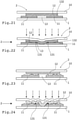
- FIG. 17 and 18 show a switch 2, comprising two carriers 1, 10, and a switch element 11 located on the carrier 1, which is interrupted in the actuation area of the switch 2 and has an interruption 13.
- a further switch element 12 which lies opposite the switch element 11 , is arranged on the region of the further carrier 10 opposite the switch element 11 .
- the further switch element 12 is designed to bridge the interruption 13 in at least one contact point 131 when force is applied normal to the direction of expansion of the carrier 1, 10 and in this way to electrically conductively connect the part of the switch element 11 that is interrupted by the interruption.
- the superimposed, electrically conductive switch elements 11, 12 are electrically insulated from one another by an insulating surface layer 110, 120, in particular made of aluminum that has been oxidized on the surface, aluminum adhesive tape, or insulating adhesive.
- an insulating surface layer 110, 120 in particular made of aluminum that has been oxidized on the surface, aluminum adhesive tape, or insulating adhesive.
- only one of the switch elements 11, 12 can have an insulating surface layer 110, 120.
- the insulating surface layer 110, 120 can also consist of other oxidizing, electrically conductive materials such as copper or conductive silver lacquer.
- FIG 19 shows a further embodiment of a switch 2, in which, as in FIG 17 Switch 2 shown, on the carrier 1, 10, a switch element 11 and a further switch element 12 are arranged opposite one another.
- An electrically insulating material 132 such as electrically insulating adhesive, is applied in a fine grid between the switch element 11 and the switch element 12.
- the application of the grid of the electrically insulating material 132 can be realized in a printing process and an interruption 13 is arranged in the actuation area of the switch 2 .
- An example of an insulating material that can be considered is an adhesive, in particular an adhesive or lacquer that is applied in a printing process and hardens under UV light.
- the flexible or pliable further switch element 12 adapts to the electrically insulating material 132 applied in a grid, so that at least two contact points 131 are formed, in which the further switch element 12 respectively one of the two connections of the switch element 11 is electrically conductively contacted or its interruption 13 is bridged, so that current can flow through the switch 2 .
- the switch 2 comprises a carrier 1, 10 and switch elements 11 and a further switch element 12, the switch 2 having a bridging 13 which is arranged in the actuation area of the switch 2.
- a layer of electrically insulating material 132 is arranged between the switch elements 11 and the further switch element 12 .
- the layer is continuous so that it completely electrically insulates the additional switch element 12 from the switch elements 11 or the interruption 13 .
- the layer of electrically insulating material 132 is an insulating resilient adhesive layer.
- the layer electrically insulating material 132 deformed or displaced. As a result, at least two contact points 131 are formed, in which the switch elements 11 electrically conductively contact the further switch element 12 so that current can flow via the switch 2 .
- the layer of electrically insulating material 132 After the end of the pressurization, the layer of electrically insulating material 132 returns to its original shape and the switch 2 is not continuously activated.
- a combination of conductive silver lacquer for forming the switch elements 11, 12 in combination with a layer of elastic adhesive as the electrically insulating material 132 is particularly suitable for forming such a switch 2.
- the switch 2 comprises a carrier 1 with a switch element 11 with two areas which are separated by an interruption 13 and which have a relief on the side facing the further carrier 10.
- a further switch element 12 is arranged on the further carrier 10 and contacts the switch elements 11 of the carrier 1 at points along the relief. Due to the fact that the contact between the switch elements 11 and the further switch element 12 is only pointwise, a sufficiently high resistance is ensured so that no current can flow via the switch 2 and the NFC chip 3 is not supplied with energy via an NFC antenna 4 .
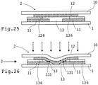
- the switch 2 comprises a carrier 1, 10 and switch elements 11 and a further switch element 12, the switch 2 having a bridging 13 which is arranged in the actuation area of the switch 2.
- a layer of electrically insulating adhesive 136 is specifically arranged between the switch element 11 and the further switch element 12 .
- the layer is continuous so that it completely electrically insulates the additional switch element 12 from the switch element 11 or the interruption 13 .
- the layer of electrically insulating adhesive 132 can be an insulating adhesive, for example.
- 26 shows the in 25 Switch 2 shown in the actuated state.
- the layer of electrically insulating material 132 is deformed or displaced.
- at least one contact point 131 is formed, in which the switch element 11 contacts the further switch element 12 in an electrically conductive manner, so that current can flow via the switch 2 .
- the layer of electrically insulating material 132 such as glue, returns to its original shape and the switch 2 is not continuously activated.
- a combination of conductive silver lacquer for forming the switch elements 11, 12 in combination with a layer of aluminum as the electrically insulating material 132 is particularly suitable for forming such a switch 2.
- a spacer can be arranged on a carrier 1, 10 in all switches shown in the area around the switch 2, so that if slight pressure is unintentionally applied to the switch 2, for example when devices 100, 100' are stacked, the switch 2 is not undesirably closed .
- a switch 2 is formed with a combination of conductive paint and other conductive material, an adhesive or paint serving as a spacer is advantageously used in the industrial production of such a switch, which is cured, for example, by UV radiation and is then no longer deformable.
- a such material is also particularly suitable for the formation of spacers for switches, since the volume remains approximately the same during curing.
- this can be achieved by applying a conventional adhesive but leaving an area free of any adhesive around the locations of the switches. This means that a certain amount of free space remains between the two switch elements 11 , 12 . Even after a high pressure order, the two layers separate again and the switch is therefore functional and not continuously active.
- the carrier 1 and the further carrier 10 are glued together and that area of the carrier 1 or the further carrier 10 within an area 137 ( 28 ) around the switch elements 11, 12 is free of adhesive.
- an additional spacer is inserted in the area around the switch 2, which at least partially surrounds the switch 2.
- Such a spacer is particularly useful and advantageous when, as is the case when magazines are stacked during transport, the individual pages are subject to high pressure.
- the additional spacer around switch 2 ensures that the layers of paper remain spaced in the wider switch area.
- Materials that can be applied in a printing process such as adhesives, in particular UV-curing adhesives, or lacquers, in particular relief lacquers, are particularly advantageous for this purpose.
- the spacer used can be applied in a grid so that the conductive materials can only be brought into electrically conductive contact and a switch 2 is triggered when pressure is applied intentionally and in a targeted manner. If the pressure is released, the switch goes back into the deactivated state.
- the device 100 according to the invention can be implemented with particularly thin paper, for example with two 40 gram layers of paper, by applying a primer to the paper for areas which would otherwise remain white, so that the electronic components and the conductive lacquer do not show through.
- the device according to the invention proves to be particularly robust and durable. This is achieved through the use of flexible materials and the smallest technical elements.
- the NFC chips 3 used can be produced with a thickness of less than 70 microns, for example. Gluing the two layers together connects them in such a way that the function remains intact even through strong bending and slight folding.
- switches 2 can also be used as switches 2, such as snap-action disks made of stainless steel.
- the snap-action disk is arranged on a carrier 1 with conductor tracks 6 , in particular on a label, and serves as a pushbutton switch that is open in its initial state, so that no electric current flows through the switch 2 .
- electrical contact is established between the snap-action disk and a conductor track 6, so that a closed circuit is formed.
- Another carrier 10 can be arranged over the snap disk and cover it so that it is not visible to a user of a device 100, 100'.
- the NFC chip 3 assigned to the respective switch 2 is supplied with electrical energy by the NFC-enabled data communication device via the NFC reader antenna 61 and transmits the information stored in it to the NFC-enabled data communication device 60 using a specified protocol.
- capable data communication device 60 processes the information it receives and executes the instructions contained therein or displays the information contained therein. For example, a link to an internet page with the NFC-enabled data communication device 60 can be called up by pressing a switch 2 on the device 100, 100' according to the invention.
- the speed of transmitting commands or the storage capacity or the possibility of not only transmitting stored commands but also actively storing information on the NFC chip 3 can be increased , to be guaranteed.
- the contacts of the NFC chip 3 are attached to the conductor tracks 7 in a contacting manner, for example using a conductive adhesive.
- the commands to be executed or the information to be displayed are stored on the carrier 1 after they have been applied to the label, in particular before the label is attached.
- information can also be stored on the NCF chip 3 after the NFC chip 3 has been attached to the device 100 according to the invention.
- the stored commands can, for example, open Internet pages on an NFC-enabled data communication device 60 or execute commands in applications stored on the NFC-enabled data communication device 60 .
- a carrier 1, 10 of a device 100 An example of the production of a carrier 1, 10 of a device 100 according to the invention is shown in more detail below.
- the position of a data communication device 60 in relation to the carrier 1 is determined and the position of the NFC antenna 4 relative to the carrier 1 is determined as a function thereof.
- a print image and a print format can be selected for the carrier 1 used to produce the device 100, 100′ according to the invention.
- the carrier 1 is preferably printed on its side opposite the conductor tracks 6 with the print image provided for this purpose or the graphics provided for this purpose.
- the conductor tracks 6 are applied to the carrier 1.
- the switches 2, 2a, ..., 2c or switch elements 11 are positioned on the carrier 1 or created on the carrier 1, for example by printing on the side of the carrier 1 facing the conductor tracks 6, .
- the NFC chips 3 assigned to a switch 2, 2a, ..., 2c are programmed with the control commands or links to be transmitted and then the label 5, 5' is applied to the carrier 1 and the contact points 80, 8a, ... , 8e, 80', 8a', ..., 8e' on the carrier 1 with the contact points 90, 9a, ..., 9e, 90', 9a', ..., 9e' of the label 5, 5' contacted.
- a further carrier 10 can also be provided, which is arranged opposite the carrier 1.
- a printed image for the side of the further carrier 10 facing away from the carrier 1 can optionally be selected for the further carrier 10 .
- the print format of the further carrier 10 is defined according to the print format of the carrier 1 and the further carrier 10 is printed with text or graphics, for example, according to the specified print image.
- further switch elements 12 are formed on the further carrier 10 in the area of the switches 2, 2a, ..., 2c on that side of the further carrier 10 which faces the conductor tracks 6 of the carrier 1 ( 30 ).
- the sides of the carrier 1 and of the further carrier 10, which face one another and are provided with the switch elements 11, 12, are joined together, in particular glued.
- a device 100, 100' can be produced in which the switch elements 11, 12 or the conductor tracks 6 and the label 5, 5' are not visible to a user. If necessary, the device 100, 100' is printed on the sides facing the user, so that the user's interest in the information or links stored on the NFC chips 3 can be effectively aroused.
- a carrier 1 printed on both sides can also be produced.
- a primer is applied to the side of the carrier 1 on which the conductor tracks 6 are located.
- a further print image is defined for that side of the carrier 1 of the device 100, 100' on which the conductor tracks 6 are located, corresponding to the print format of the carrier 1. Subsequently, the carrier 1 is overprinted on its side facing the conductor tracks 6 with the selected further printed image.
- a device 100, 100' can also be created using a single carrier 1, which is printed on both of its sides facing the user.
- the switches require those supplementary further switch elements 12 which can be formed, for example, on the further carrier 10 and would have to be supplemented in such implementations with only one carrier 1 .
- by attaching further labels 14 at the locations of the switch elements 11, those further switch elements 12, as well as other known flat switches, can be supplemented here.
- a device 100, 100' according to the invention can be used, for example, in the printing area for advertisements designed as flyers, brochures or posters or also advertisements in magazines, for example.
- a device 100, 100' according to the invention for example further training materials, handouts, product inserts, packaging or menus can also be designed so that a user can use them interactively.
- the preparation of the individual NFC chips for the printing process can be done in different ways. It is of particular importance for some of the manufacturing methods shown here that for devices 100' according to the invention the individual NFC chips are equipped a priori by their label 5' without an NFC antenna 4, and thus without the presence of an NFC antenna 4 on the label 5' must be written with the respective data sets. However, many NFC chips are designed so that the memory located in the NFC chip can only be written to or programmed with a connected, permanently active NFC antenna 4 . A particularly advantageous method of programming such NFC chips is in 31 shown in more detail.
- the in 30 circuit arrangement shown created In order to be able to flexibly describe the NFC chips 3 of the label 5' with the associated data sets, the in 30 circuit arrangement shown created.
- the NFC chip 3 in question is connected to one side or coil L 2 of a transformer T with its two connections.
- a programming unit 30 is connected, which is designed to use an NFC chip 3 using two to program coupled coils. Instead of using two coils, it is provided in the present case to provide a capacitor C parallel to the coil L 2 of the transformer T, which is dimensioned such that the resulting LC resonant circuit connected to the programming unit 30 resonates at 13.56 MHz.
- the NFC-enabled data communication device 60 is associated with the respective active NFC tag 70 or the NFC antenna 4 of that tag 70, as shown schematically in 2 shown, countered.
- the NFC-enabled data communication device 60 is placed on the marking 22 of the device 100, 100' in order to interact with the NFC by actuating the switch 2 of the device 100, 100' -enabled data communication device 60 to allow.
- an NFC antenna 4 is used in the device 100, 100', the size and shape of which is optimally adapted to the NFC -Reader antennas 61 common NFC-enabled data communication devices 60 are adapted.
- the coil size in conventional NFC antennas 4 of conventional NFC tags 70 is kept relatively small, for example in the range of 38 x 38 mm, it is with the large number of positions that the NFC reader antennas 61 in conventional NFC-enabled Data communication devices 60, in particular NFC-enabled smartphones, difficult to establish NFC data communication with different NFC-enabled data communication devices 60, provided that it is provided that the marking 22 of the respective device 100, 100 ', on which the NFC-enabled data communication device 60 placed in each case is uniform in shape and size.
- an NFC antenna 4 is advantageously used, the size and shape of which, with similar positioning of NFC-enabled data communication devices 60, in particular NFC-enabled smartphones, with regard to the device 100, 100 ', covers a maximum number of positions of NFC reader antennas 61 in NFC-enabled data communication devices 60, in particular NFC-enabled smartphones, or at least overlaps in a certain area in order to place a wide variety of NFC capable data communication devices 60 on the marking 22 of the device 100, 100 'a coupling between the voltage field, which emanates from the NFC reader antenna 61 of the NFC-enabled data communication device 60, and the voltage field on the carrier 1 or the label 5 located NFC antenna 4 to create.
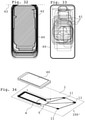
- FIG. 32 shows a graphic in which the outlines of 37 different, common NFC-enabled data communication devices 60, or smartphones, are shown overlapping. These are each aligned centrally on the upper edge 63 of the marking 22, since, for behavioral reasons, users tend, when positioning their NFC-enabled data communication device 60 on the device 100, 100', to position it on the upper edge 63 of the marking 22 on the device 100, 100 ' align.
- the NFC-enabled data communication devices 60 can also be aligned at any other types of uniformly defined locations, provided this is expedient for the result. For example, a point can be selected based on which the center point of the corresponding NFC-enabled data communication device 60 is aligned.
- the position of the NFC reader antenna 61 of the respective NFC-enabled data communication device 60 is marked in the outlines of common NFC-enabled data communication devices 60 ( Figure 33 ). Overall, these different placements lead to a surface area 62 or an overall scheme of positions of NFC reader antennas 61 of the NFC-enabled data communication devices 60, which in 32 is marked.
- the surface area 62 has approximately external dimensions of 70 ⁇ 140 mm ( 32 ).
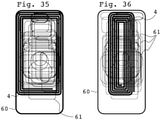
- this approach to creating the NFC antenna design results in the antenna size and shape, such as in the in Figure 35 illustrated NFC antenna 4, a variety of NFC reader antennas 61 of NFC-enabled Data communication devices 60 covers an area in an appropriate area, and thus optimally fulfills the purpose of the broadest possible functionality.
- the main advantage of an NFC antenna 4 designed in this way is that the user does not have to move his mobile NFC-enabled data communication device 60 several times and try different positions in order to establish NFC communication and, for example, to be able to open links, as is the case with the antenna sizes and -Forms of conventional NFC tags 70 would be the case if they were used in a device 100, 100' according to the invention.
- a simple and direct execution of the desired interaction is made possible, since the probability of a coupling of the NFC reader antennas 61 of the respective mobile data communication device 60 with the NFC antenna 4 of the device 100, 100' is maximized due to the large area coverage will.
- a width of 60 to 80 mm and a height of 110 to 150 mm ( Figure 35 ).
- the carrier 1 is a paper in DIN A4 format 210 x 297 mm and the printed NFC antenna 4 has external dimensions of 74 x 131 mm.
- the four turns are each 2.2 mm wide.
- the number of turns proves to be a particularly significant performance feature of the NFC antenna 4. provided the width of the turns in is located in an area less than 3 mm, four turns are sufficient so that the total resistance of the NFC antenna 4 does not significantly exceed twenty-five (25) ohms, provided that the NFC antenna is screen printed on paper with common screen printable silver conductive inks and the specifications of the used Corresponding to conductive silver lacquer is dried. If the number of turns is increased, then the reception range of the NFC antenna 4 is increased. The resistance can be reduced by applying the antenna material higher and wider, as well as by using a suitable substrate, which has proven to promote electrical conductivity.
- the NFC antenna 4 is printed with an electrically conductive lacquer, for example with conductive silver lacquer, coated paper with a surface that is as smooth as possible often proves to be particularly suitable.
- Rough papers tend to absorb the applied materials more, which means that the conductivity of the conductive varnish is inhibited by the influence of paper fibers.
- the number of turns also plays a role with regard to the reception strength of the NFC antenna 4 in that interaction of the parameters.
- the width of the NFC antenna 4 can be reduced from 60 to 80 mm to about 40 to 45 mm if the NFC antenna 4 is added a fifth or sixth turn inward, depending on the extent of the width reduction to compensate for the size reduction with a stronger frequency of the NFC antenna 4 ( Figure 36 ).
Landscapes
- Engineering & Computer Science (AREA)
- Microelectronics & Electronic Packaging (AREA)
- Computer Hardware Design (AREA)
- Physics & Mathematics (AREA)
- General Physics & Mathematics (AREA)
- Theoretical Computer Science (AREA)
- Computer Networks & Wireless Communication (AREA)
- Near-Field Transmission Systems (AREA)
- Details Of Aerials (AREA)
Claims (13)
- Dispositif (100, 100'), en particulier produit imprimé, comprenant- un support (1), de préférence flexible, en particulier constitué de papier ou de carton,- un certain nombre de commutateurs (2 ; 2a, 2b, ...) disposés sur le support (1) et interrompus dans leur état initial respectif,- un nombre de puces NFC (3 ; 3a, 3b, ...) associées respectivement à au moins un commutateur,- une antenne NFC (4),- dans lequel les commutateurs (2 ; 2a, 2b, ...) et les puces NFC (3 ; 3a, 3b, ...) qui leur sont associées sont montés en série les uns avec les autres et les circuits en série individuels ainsi réalisés comprenant respectivement un commutateur (2 ; 2a, 2b, ...) et la puce NFC (3 ; 3a, 3b, ...) qui lui est associée sont respectivement raccordés à l'antenne NFC (4),caractérisé en ce- que le dispositif comprend une étiquette (5 ; 5') avec un corps de base (50) en forme de feuille, dans lequel l'étiquette (5 ; 5') est mise en liaison à plat avec le support (1),- que les puces NFC individuelles (3 ; 3a, 3b, ...) sont disposées sur l'étiquette (5 ; 5'),- que les commutateurs (2 ; 2a, 2b, ...) sont disposés sur le support (1) dans une zone différente de l'étiquette (5 ; 5'),- que, pour la connexion électrique des commutateurs (2 ; 2a, 2b, ...), des puces NFC (3 ; 3a, 3b, ...) et de l'antenne NFC (4), des pistes conductrices (6, 7) sont prévues sur le support (1), le cas échéant aussi sur l'étiquette (5 ; 5'), et- que sont prévus sur l'étiquette (5 ; 5') et sur le support (1) des points de contact (80, 8a, 8b, ..., 90, 9a, 9b, ..., 80', 8a', 8b', ..., 90', 9a', 9b', ...) tournés les uns vers les autres, qui mettent en contact électriquement conducteur les pistes conductrices (6, 7) sur l'étiquette (5 ; 5') et sur le support (1).
- Dispositif (100, 100') selon la revendication 1, caractérisé en ce que les pistes conductrices (6, 7) sur l'étiquette (5 ; 5') et/ou sur le support (1) sont des couches électriquement conductrices, qui sont réalisées en particulier avec un vernis électriquement conducteur ou avec une encre ou un film électriquement conducteur ou qui en sont constituées.
- Dispositif (100, 100') selon la revendication 1 ou 2, caractérisé en ce que les points de contact (80, 8a, 8b, ..., 90, 9a, 9b, ..., 80', 8a', 8b', ..., 90', 9a', 9b', ...) tournés les uns vers les autres, en particulier du support (1, 10), sont des couches électriquement conductrices, qui sont réalisées en particulier avec un vernis conducteur, un film conducteur ou une encre électriquement conductrice ou qui en sont constituées, dans lequel la couche conductrice et/ou les points de contact sont réalisés de manière à être conducteurs en surface, de préférence de manière non oxydante.
- Dispositif (100, 100') selon l'une quelconque des revendications précédentes, caractérisé en ce que l'antenne NFC (4) est disposée sur l'étiquette (5).
- Dispositif (100, 100') selon l'une quelconque des revendications précédentes, caractérisé par un support supplémentaire (10), en particulier en papier ou en carton, de préférence constitué du même matériau que le support (1), dans lequel l'étiquette (5 ; 5') est disposée entre les deux supports (1, 10).
- Dispositif (100, 100') selon la revendication 5, caractérisé en ce qu'au moins un des commutateurs (2 ; 2a, 2b, ...) est réalisé par deux éléments de commutation (11, 12) disposés l'un en face de l'autre sur le support (1) et sur le support supplémentaire (10) et tournés l'un vers l'autre, dans lequel au moins un des éléments de commutation (11, 12) présente une couche superficielle isolante (110, 120) tournée vers l'autre élément de commutation respectif, en particulier une couche d'oxyde, qui est de préférence disposée entre les deux éléments de commutation (11, 12) et isole ceux-ci électriquement l'un de l'autre dans l'état initial,
en particulier en ce que les éléments de commutation (11, 12) sont disposés de sorte que l'au moins une couche superficielle isolante (110, 120) d'un des éléments de commutation (11, 12), en cas d'application d'une force perpendiculaire au plan d'extension du support (1), le cas échéant se rompt ou se déchire ou se déforme élastiquement et qu'un contact se produit entre les deux éléments de commutation (11, 12) et que le commutateur (2 ; 2a, 2b, ...) se trouve ainsi à l'état activé. - Dispositif (100, 100') selon la revendication 6, caractérisé en ce- que les éléments de commutation (11) s'étendant sur le support (1) présentent deux raccords interrompus par une interruption (13), qui sont isolés électriquement l'un de l'autre dans l'état initial, et- que sur la zone du support supplémentaire (10) opposée aux éléments de commutation (11), des éléments de commutation supplémentaires (12) sont disposés, qui sont conçus pour entrer en contact électriquement conducteur avec chacun des raccords de l'élément de commutation (11) respectivement associé en cas d'application d'une force, de manière à ponter l'interruption (13) et à relier de manière électriquement conductrice les raccords de l'élément de commutation (11) respectif qui sont électriquement séparées l'une de l'autre par l'interruption (13).
- Dispositif (100, 100') selon la revendication 6 ou 7, caractérisé en ce qu'au moins un des éléments de commutation (11), le cas échéant les deux éléments de commutation (11, 12), est recouvert d'une couche de matériau conducteur avec un revêtement isolant en surface, en particulier en aluminium oxydé en surface, ou avec un matériau conducteur en surface, en particulier une laque conductrice d'argent, laquelle est de préférence revêtue d'un matériau partiellement appliqué, durcissant et de préférence électriquement isolant, en particulier d'une laque ou d'une colle à haut pouvoir d'application et durcissant aux UV, et dans lequel, le cas échéant, l'élément de commutation opposé est réalisé avec un matériau électriquement conducteur en surface, en particulier une laque conductrice d'argent,
dans lequel en particulier le support (1) et le support supplémentaire (10) sont collés l'un à l'autre, et la zone respective du support (1) et/ou du support supplémentaire (10) dans la zone des éléments de commutation (11, 12) et de préférence aussi à l'intérieur d'un environnement (137) autour des éléments de commutation (11, 12) est exempte de la colle reliant les deux supports (1 ; 10) l'un à l'autre. - Dispositif (100, 100') selon l'une quelconque des revendications précédentes, caractérisé en ce que les commutateurs (2 ; 2a, 2b, ...) sont respectivement disposés séparément sur des étiquettes supplémentaires (14), dans lequel ces étiquettes supplémentaires (14) sont disposées sur le support (1), le cas échéant entre les supports (1, 10) ou sur un des supports (1, 10).
- Dispositif (100) selon l'une quelconque des revendications précédentes, caractérisé en ce- que l'antenne NFC (4) et les puces NFC (3 ; 3a, 3b, ...) sont disposées sur l'étiquette (5),- que l'antenne NFC (4) est réalisée sur l'étiquette (5), en particulier par impression, gravure ou estampage, et présente une pluralité de spires (15) ainsi qu'un raccord intérieur (16) et un raccord extérieur (17), et- qu'un pontage (18) est prévu, qui est relié de manière électriquement conductrice au raccord intérieur (16), dans lequel le pontage (18) est guidé de manière isolée des spires (15) dans la zone à l'extérieur de l'antenne NFC (4),- que respectivement l'un des raccords de chacune des puces NFC (3 ; 3a, 3b, ...) se trouvant sur l'étiquette (5) est relié de manière électriquement conductrice à respectivement un point de contact (9a, 9b, ...),- que l'autre raccord respectif de chacune des puces NFC (3; 3a, 3b, ...) se trouvant sur l'étiquette (5) est relié de manière électriquement conductrice au raccord intérieur (16) de l'antenne NFC (4) par l'intermédiaire du pontage (18),- que le raccord extérieur (17) de l'antenne NFC (4) est raccordé de manière électriquement conductrice à un point de contact supplémentaire (90) disposé sur l'étiquette (5), et- que chacun des points de contact (9a, 9b, ...) est relié de manière électriquement conductrice au raccord extérieur (17) par l'intermédiaire d'une piste conductrice (6) s'étendant sur le support (1), par l'intermédiaire du point de contact supplémentaire (90'), dans lequel un commutateur (2 ; 2a, 2b, ...) interrompu à l'état initial est disposé dans chacune de ces pistes conductrices (6).
- Dispositif (100') selon l'une quelconque des revendications précédentes 1 à 3 ou 5 à 9, caractérisé en ce- que l'antenne NFC (4) est réalisée sur le support (1), en particulier par impression, gravure ou estampage, et présente une pluralité de spires (15) ainsi qu'un raccord intérieur (16) et un raccord extérieur (17), et dans lequel les spires individuelles (15) de l'antenne NFC (4) s'étendent à distance les unes des autres, en particulier parallèlement, dans au moins une zone de pontage (51),- que l'étiquette (5') est disposée sur la zone de pontage (51) de manière à dépasser et présente un point de contact (90) qui est en contact électriquement conducteur avec le raccord intérieur (16) de l'antenne NFC (4),- que respectivement un raccord des puces NFC (3 ; 3a, 3b, ...) se trouvant sur l'étiquette (5') est relié de manière électriquement conductrice à ce point de contact (90), et- que l'autre raccord respectif de chacune des puces NFC (3 ; 3a, 3b, ...) se trouvant sur l'étiquette (5') est en contact conducteur avec un point de contact supplémentaire (9a, 9b, ...) avec une zone du support (1), qui se trouve à l'extérieur de l'antenne NFC (4), et- que chacun des points de contact supplémentaires (9a, 9b, ...) est relié de manière électriquement conductrice au raccord extérieur (17) de l'antenne NFC (4) par l'intermédiaire respectivement d'une des pistes conductrices (6) s'étendant sur le support (1), dans lequel un commutateur (2 ; 2a, 2b, ...) interrompu à l'état initial étant disposé respectivement dans chacune des pistes conductrices (6).
- Dispositif selon l'une quelconque des revendications précédentes, caractérisé en ce que l'antenne NFC (4)- présente des dimensions extérieures avec une largeur de 40 à 80 mm, en particulier de 60 à 80 mm, et une hauteur de 110 à 150 mm, de préférence une largeur de 74 mm et une hauteur de 131 mm, et/ou- présente un nombre de 3 à 7 spires, en particulier avec une épaisseur de ligne respectivement inférieure à 3 mm, de préférence 4 spires avec une épaisseur de ligne de 1,5 à 2,5 mm et une épaisseur de couche inférieure ou égale à 40 µm, en particulier lorsque l'antenne NFC (4) est imprimée sur papier au moyen d'un vernis conducteur d'argent par sérigraphie, et/ou- présente en particulier une résistance totale inférieure ou égale à 25 ohms.
- Disposition comprenant un dispositif (100, 100') selon l'une quelconque des revendications 1 à 12, ainsi qu'un appareil de communication de données (60) compatible NFC, qui est en liaison de communication de données avec une des puces NFC (3 ; 3a, 3b, ...) par l'intermédiaire de l'antenne NFC (4) lors de l'actionnement d'un des commutateurs.
Applications Claiming Priority (5)
| Application Number | Priority Date | Filing Date | Title |
|---|---|---|---|
| AT600492017 | 2017-06-09 | ||
| AT600842017 | 2017-09-03 | ||
| AT601292017 | 2017-11-19 | ||
| AT500422018 | 2018-01-19 | ||
| PCT/AT2018/060119 WO2018223171A2 (fr) | 2017-06-09 | 2018-06-08 | Dispositif, en particulier produit d'impression pour la communication de données |
Publications (2)
| Publication Number | Publication Date |
|---|---|
| EP3635635A2 EP3635635A2 (fr) | 2020-04-15 |
| EP3635635B1 true EP3635635B1 (fr) | 2022-02-16 |
Family
ID=62904205
Family Applications (1)
| Application Number | Title | Priority Date | Filing Date |
|---|---|---|---|
| EP18740085.8A Active EP3635635B1 (fr) | 2017-06-09 | 2018-06-08 | Dispositif, en particulier produit d'impression pour la communication de données |
Country Status (3)
| Country | Link |
|---|---|
| US (1) | US11941473B2 (fr) |
| EP (1) | EP3635635B1 (fr) |
| WO (1) | WO2018223171A2 (fr) |
Families Citing this family (8)
| Publication number | Priority date | Publication date | Assignee | Title |
|---|---|---|---|---|
| DE112019006728T5 (de) * | 2019-01-25 | 2021-10-28 | Murata Manufacturing Co., Ltd. | Drahtloskommunikationsvorrichtung und verfahren zum herstellen derselben |
| GB201904770D0 (en) * | 2019-04-04 | 2019-05-22 | Tech 21 Licensing Ltd | A case for mobile device with a screen |
| ES2986961T3 (es) | 2019-05-22 | 2024-11-13 | Bayer Ag | Monitoreo de productos |
| TWI713250B (zh) * | 2019-10-05 | 2020-12-11 | 啓碁科技股份有限公司 | 通訊裝置和通訊方法 |
| JP2024533936A (ja) | 2021-08-13 | 2024-09-18 | ジェイティー インターナショナル エスエイ | ディスプレイ及びユーザインターフェースを有する電子デバイスを他の電子デバイスにリンクさせるためのスマートペーパ又はシート |
| WO2025158074A1 (fr) * | 2024-01-25 | 2025-07-31 | Fechtig Andreas | Carte de crédit personnalisée et procédé de réalisation de transaction financière avec la carte de crédit |
| CH721549A1 (de) * | 2024-01-25 | 2025-07-31 | Fechtig Andreas | Multiple karte und verfahren zur durchführung einer finanztransaktion mit der karte |
| CN121168481B (zh) * | 2025-09-04 | 2026-04-10 | 深圳市富卡思通物联科技有限公司 | 一种单个芯片扩展多个nfc天线标签及其生产工艺、标签通讯方法 |
Family Cites Families (7)
| Publication number | Priority date | Publication date | Assignee | Title |
|---|---|---|---|---|
| US7762471B2 (en) | 2006-09-07 | 2010-07-27 | Mastercard International, Inc. | Proximity payment card with cost-effective connection between user-actuatable input switch and RFID IC |
| US20080094181A1 (en) | 2006-10-24 | 2008-04-24 | Tagsys Sas | Passive remote control |
| KR101688140B1 (ko) * | 2010-05-19 | 2016-12-20 | 엘지전자 주식회사 | 키조립체 및 이를 구비하는 이동 단말기 |
| DE102013223505B3 (de) * | 2013-11-18 | 2014-11-20 | F & R Innovations UG (haftungsbeschränkt) | NFC-Auslesevorrichtung |
| KR101626503B1 (ko) * | 2014-11-27 | 2016-06-01 | 주식회사 아이엠에이 | 탈부착식 버튼형 nfc 태그를 이용한 스마트 단말의 매크로 실행 시스템 및 방법 |
| US20160180210A1 (en) | 2014-12-22 | 2016-06-23 | Christopher Steele Spears | Multifunction contactless smart chip device with integrated user actuated switch |
| CN105893893B (zh) * | 2015-01-26 | 2020-08-11 | 北京搜狗科技发展有限公司 | 一种信息处理方法、电子设备及nfc卡片 |
-
2018
- 2018-06-08 EP EP18740085.8A patent/EP3635635B1/fr active Active
- 2018-06-08 WO PCT/AT2018/060119 patent/WO2018223171A2/fr not_active Ceased
- 2018-06-08 US US16/620,688 patent/US11941473B2/en active Active
Also Published As
| Publication number | Publication date |
|---|---|
| US11941473B2 (en) | 2024-03-26 |
| WO2018223171A2 (fr) | 2018-12-13 |
| US20200125917A1 (en) | 2020-04-23 |
| EP3635635A2 (fr) | 2020-04-15 |
| WO2018223171A3 (fr) | 2020-01-09 |
Similar Documents
| Publication | Publication Date | Title |
|---|---|---|
| EP3635635B1 (fr) | Dispositif, en particulier produit d'impression pour la communication de données | |
| DE69706280T2 (de) | Kontaktloses elektronisches modul für karte oder etikette | |
| EP2036001B1 (fr) | Transpondeur comprenant une puce mémoire électronique et une antenne circulaire magnétique | |
| DE10016037B4 (de) | Verfahren zur Herstellung eines Etiketts oder einer Chipkarte | |
| EP3818475B1 (fr) | Transpondeur à double bande et etiquette avec transpondeur à double bande | |
| EP0967568A2 (fr) | Elément d'identification | |
| DE102014114570A1 (de) | Verstärkerantennenstruktur | |
| EP3231254B1 (fr) | Module de del | |
| EP1375131A1 (fr) | Laminé ayant une couche conductrice servant d'antenne | |
| EP2875472B1 (fr) | Moyen d'identification de véhicule | |
| EP2338207A1 (fr) | Antenne pour balise rfid | |
| EP2263194A1 (fr) | Structure d' antenne avec au moins deux bobines-antennes; composant rf pour la transmission sans contact d' énergie et de données; appareil électronique avec composant rf | |
| EP1028388B1 (fr) | Elément d'identification et procédé de fabrication d'un élément d'identification | |
| EP1527413B1 (fr) | Support de donnees avec solenoide de transpondeur | |
| EP1877967B1 (fr) | Procédé de fabrication d'un support de données portable | |
| DE202010014408U1 (de) | Baugruppe mit wenigstens einer UHF-Dipol-Antenne | |
| DE102006044881A1 (de) | Tragbarer Datenträger und Verfahren zum Betreiben eines tragbaren Datenträgers | |
| DE102008022711A1 (de) | Raumgebilde mit einem Transponder und Verfahren zum Erzeugen desselben | |
| DE4428732C1 (de) | Mehrlagige Chipkartenspulen für kontaktfreie Chipkarten | |
| EP4437453A1 (fr) | Support de stockage de données sous forme de carte et procédé de fabrication d'un support de stockage de données sous forme de carte | |
| DE102005016511B4 (de) | Verfahren zum Herstellen einer Leiterstruktur auf einem Substrat | |
| EP2430593B1 (fr) | Support d'impression interactif | |
| DE102008024487B4 (de) | Halbleitervorrichtung mit integrierter Spule und Verfahren zu deren Herstellung | |
| DE102006001777B4 (de) | Verfahren zum Erzeugen eines Raumgebildes mit einem Transponder | |
| EP1162480A2 (fr) | Transpondeur sans contact |
Legal Events
| Date | Code | Title | Description |
|---|---|---|---|
| STAA | Information on the status of an ep patent application or granted ep patent |
Free format text: STATUS: UNKNOWN |
|
| STAA | Information on the status of an ep patent application or granted ep patent |
Free format text: STATUS: THE INTERNATIONAL PUBLICATION HAS BEEN MADE |
|
| PUAI | Public reference made under article 153(3) epc to a published international application that has entered the european phase |
Free format text: ORIGINAL CODE: 0009012 |
|
| STAA | Information on the status of an ep patent application or granted ep patent |
Free format text: STATUS: REQUEST FOR EXAMINATION WAS MADE |
|
| 17P | Request for examination filed |
Effective date: 20191209 |
|
| AK | Designated contracting states |
Kind code of ref document: A2 Designated state(s): AL AT BE BG CH CY CZ DE DK EE ES FI FR GB GR HR HU IE IS IT LI LT LU LV MC MK MT NL NO PL PT RO RS SE SI SK SM TR |
|
| AX | Request for extension of the european patent |
Extension state: BA ME |
|
| DAV | Request for validation of the european patent (deleted) | ||
| DAX | Request for extension of the european patent (deleted) | ||
| GRAP | Despatch of communication of intention to grant a patent |
Free format text: ORIGINAL CODE: EPIDOSNIGR1 |
|
| STAA | Information on the status of an ep patent application or granted ep patent |
Free format text: STATUS: GRANT OF PATENT IS INTENDED |
|
| INTG | Intention to grant announced |
Effective date: 20210903 |
|
| GRAS | Grant fee paid |
Free format text: ORIGINAL CODE: EPIDOSNIGR3 |
|
| GRAA | (expected) grant |
Free format text: ORIGINAL CODE: 0009210 |
|
| STAA | Information on the status of an ep patent application or granted ep patent |
Free format text: STATUS: THE PATENT HAS BEEN GRANTED |
|
| AK | Designated contracting states |
Kind code of ref document: B1 Designated state(s): AL AT BE BG CH CY CZ DE DK EE ES FI FR GB GR HR HU IE IS IT LI LT LU LV MC MK MT NL NO PL PT RO RS SE SI SK SM TR |
|
| REG | Reference to a national code |
Ref country code: GB Ref legal event code: FG4D Free format text: NOT ENGLISH |
|
| REG | Reference to a national code |
Ref country code: CH Ref legal event code: EP |
|
| REG | Reference to a national code |
Ref country code: DE Ref legal event code: R096 Ref document number: 502018008797 Country of ref document: DE |
|
| REG | Reference to a national code |
Ref country code: AT Ref legal event code: REF Ref document number: 1469361 Country of ref document: AT Kind code of ref document: T Effective date: 20220315 |
|
| REG | Reference to a national code |
Ref country code: IE Ref legal event code: FG4D Free format text: LANGUAGE OF EP DOCUMENT: GERMAN |
|
| REG | Reference to a national code |
Ref country code: NL Ref legal event code: FP |
|
| REG | Reference to a national code |
Ref country code: SE Ref legal event code: TRGR |
|
| REG | Reference to a national code |
Ref country code: LT Ref legal event code: MG9D |
|
| PG25 | Lapsed in a contracting state [announced via postgrant information from national office to epo] |
Ref country code: RS Free format text: LAPSE BECAUSE OF FAILURE TO SUBMIT A TRANSLATION OF THE DESCRIPTION OR TO PAY THE FEE WITHIN THE PRESCRIBED TIME-LIMIT Effective date: 20220216 Ref country code: PT Free format text: LAPSE BECAUSE OF FAILURE TO SUBMIT A TRANSLATION OF THE DESCRIPTION OR TO PAY THE FEE WITHIN THE PRESCRIBED TIME-LIMIT Effective date: 20220616 Ref country code: NO Free format text: LAPSE BECAUSE OF FAILURE TO SUBMIT A TRANSLATION OF THE DESCRIPTION OR TO PAY THE FEE WITHIN THE PRESCRIBED TIME-LIMIT Effective date: 20220516 Ref country code: LT Free format text: LAPSE BECAUSE OF FAILURE TO SUBMIT A TRANSLATION OF THE DESCRIPTION OR TO PAY THE FEE WITHIN THE PRESCRIBED TIME-LIMIT Effective date: 20220216 Ref country code: HR Free format text: LAPSE BECAUSE OF FAILURE TO SUBMIT A TRANSLATION OF THE DESCRIPTION OR TO PAY THE FEE WITHIN THE PRESCRIBED TIME-LIMIT Effective date: 20220216 Ref country code: ES Free format text: LAPSE BECAUSE OF FAILURE TO SUBMIT A TRANSLATION OF THE DESCRIPTION OR TO PAY THE FEE WITHIN THE PRESCRIBED TIME-LIMIT Effective date: 20220216 Ref country code: BG Free format text: LAPSE BECAUSE OF FAILURE TO SUBMIT A TRANSLATION OF THE DESCRIPTION OR TO PAY THE FEE WITHIN THE PRESCRIBED TIME-LIMIT Effective date: 20220516 |
|
| PG25 | Lapsed in a contracting state [announced via postgrant information from national office to epo] |
Ref country code: PL Free format text: LAPSE BECAUSE OF FAILURE TO SUBMIT A TRANSLATION OF THE DESCRIPTION OR TO PAY THE FEE WITHIN THE PRESCRIBED TIME-LIMIT Effective date: 20220216 Ref country code: LV Free format text: LAPSE BECAUSE OF FAILURE TO SUBMIT A TRANSLATION OF THE DESCRIPTION OR TO PAY THE FEE WITHIN THE PRESCRIBED TIME-LIMIT Effective date: 20220216 Ref country code: GR Free format text: LAPSE BECAUSE OF FAILURE TO SUBMIT A TRANSLATION OF THE DESCRIPTION OR TO PAY THE FEE WITHIN THE PRESCRIBED TIME-LIMIT Effective date: 20220517 Ref country code: FI Free format text: LAPSE BECAUSE OF FAILURE TO SUBMIT A TRANSLATION OF THE DESCRIPTION OR TO PAY THE FEE WITHIN THE PRESCRIBED TIME-LIMIT Effective date: 20220216 |
|
| PG25 | Lapsed in a contracting state [announced via postgrant information from national office to epo] |
Ref country code: IS Free format text: LAPSE BECAUSE OF FAILURE TO SUBMIT A TRANSLATION OF THE DESCRIPTION OR TO PAY THE FEE WITHIN THE PRESCRIBED TIME-LIMIT Effective date: 20220617 |
|
| PG25 | Lapsed in a contracting state [announced via postgrant information from national office to epo] |
Ref country code: SM Free format text: LAPSE BECAUSE OF FAILURE TO SUBMIT A TRANSLATION OF THE DESCRIPTION OR TO PAY THE FEE WITHIN THE PRESCRIBED TIME-LIMIT Effective date: 20220216 Ref country code: SK Free format text: LAPSE BECAUSE OF FAILURE TO SUBMIT A TRANSLATION OF THE DESCRIPTION OR TO PAY THE FEE WITHIN THE PRESCRIBED TIME-LIMIT Effective date: 20220216 Ref country code: RO Free format text: LAPSE BECAUSE OF FAILURE TO SUBMIT A TRANSLATION OF THE DESCRIPTION OR TO PAY THE FEE WITHIN THE PRESCRIBED TIME-LIMIT Effective date: 20220216 Ref country code: EE Free format text: LAPSE BECAUSE OF FAILURE TO SUBMIT A TRANSLATION OF THE DESCRIPTION OR TO PAY THE FEE WITHIN THE PRESCRIBED TIME-LIMIT Effective date: 20220216 Ref country code: DK Free format text: LAPSE BECAUSE OF FAILURE TO SUBMIT A TRANSLATION OF THE DESCRIPTION OR TO PAY THE FEE WITHIN THE PRESCRIBED TIME-LIMIT Effective date: 20220216 Ref country code: CZ Free format text: LAPSE BECAUSE OF FAILURE TO SUBMIT A TRANSLATION OF THE DESCRIPTION OR TO PAY THE FEE WITHIN THE PRESCRIBED TIME-LIMIT Effective date: 20220216 |
|
| REG | Reference to a national code |
Ref country code: DE Ref legal event code: R097 Ref document number: 502018008797 Country of ref document: DE |
|
| PG25 | Lapsed in a contracting state [announced via postgrant information from national office to epo] |
Ref country code: AL Free format text: LAPSE BECAUSE OF FAILURE TO SUBMIT A TRANSLATION OF THE DESCRIPTION OR TO PAY THE FEE WITHIN THE PRESCRIBED TIME-LIMIT Effective date: 20220216 |
|
| PLBE | No opposition filed within time limit |
Free format text: ORIGINAL CODE: 0009261 |
|
| STAA | Information on the status of an ep patent application or granted ep patent |
Free format text: STATUS: NO OPPOSITION FILED WITHIN TIME LIMIT |
|
| 26N | No opposition filed |
Effective date: 20221117 |
|
| PG25 | Lapsed in a contracting state [announced via postgrant information from national office to epo] |
Ref country code: MC Free format text: LAPSE BECAUSE OF FAILURE TO SUBMIT A TRANSLATION OF THE DESCRIPTION OR TO PAY THE FEE WITHIN THE PRESCRIBED TIME-LIMIT Effective date: 20220216 |
|
| REG | Reference to a national code |
Ref country code: BE Ref legal event code: MM Effective date: 20220630 |
|
| PG25 | Lapsed in a contracting state [announced via postgrant information from national office to epo] |
Ref country code: SI Free format text: LAPSE BECAUSE OF FAILURE TO SUBMIT A TRANSLATION OF THE DESCRIPTION OR TO PAY THE FEE WITHIN THE PRESCRIBED TIME-LIMIT Effective date: 20220216 |
|
| PG25 | Lapsed in a contracting state [announced via postgrant information from national office to epo] |
Ref country code: LU Free format text: LAPSE BECAUSE OF NON-PAYMENT OF DUE FEES Effective date: 20220608 |
|
| PG25 | Lapsed in a contracting state [announced via postgrant information from national office to epo] |
Ref country code: BE Free format text: LAPSE BECAUSE OF NON-PAYMENT OF DUE FEES Effective date: 20220630 |
|
| P01 | Opt-out of the competence of the unified patent court (upc) registered |
Effective date: 20230621 |
|
| PG25 | Lapsed in a contracting state [announced via postgrant information from national office to epo] |
Ref country code: IT Free format text: LAPSE BECAUSE OF FAILURE TO SUBMIT A TRANSLATION OF THE DESCRIPTION OR TO PAY THE FEE WITHIN THE PRESCRIBED TIME-LIMIT Effective date: 20220216 |
|
| PG25 | Lapsed in a contracting state [announced via postgrant information from national office to epo] |
Ref country code: MK Free format text: LAPSE BECAUSE OF FAILURE TO SUBMIT A TRANSLATION OF THE DESCRIPTION OR TO PAY THE FEE WITHIN THE PRESCRIBED TIME-LIMIT Effective date: 20220216 Ref country code: CY Free format text: LAPSE BECAUSE OF FAILURE TO SUBMIT A TRANSLATION OF THE DESCRIPTION OR TO PAY THE FEE WITHIN THE PRESCRIBED TIME-LIMIT Effective date: 20220216 |
|
| PG25 | Lapsed in a contracting state [announced via postgrant information from national office to epo] |
Ref country code: HU Free format text: LAPSE BECAUSE OF FAILURE TO SUBMIT A TRANSLATION OF THE DESCRIPTION OR TO PAY THE FEE WITHIN THE PRESCRIBED TIME-LIMIT; INVALID AB INITIO Effective date: 20180608 |
|
| PG25 | Lapsed in a contracting state [announced via postgrant information from national office to epo] |
Ref country code: TR Free format text: LAPSE BECAUSE OF FAILURE TO SUBMIT A TRANSLATION OF THE DESCRIPTION OR TO PAY THE FEE WITHIN THE PRESCRIBED TIME-LIMIT Effective date: 20220216 |
|
| PG25 | Lapsed in a contracting state [announced via postgrant information from national office to epo] |
Ref country code: MT Free format text: LAPSE BECAUSE OF FAILURE TO SUBMIT A TRANSLATION OF THE DESCRIPTION OR TO PAY THE FEE WITHIN THE PRESCRIBED TIME-LIMIT Effective date: 20220216 |
|
| PGFP | Annual fee paid to national office [announced via postgrant information from national office to epo] |
Ref country code: DE Payment date: 20250618 Year of fee payment: 8 |
|
| PGFP | Annual fee paid to national office [announced via postgrant information from national office to epo] |
Ref country code: GB Payment date: 20250618 Year of fee payment: 8 |
|
| PGFP | Annual fee paid to national office [announced via postgrant information from national office to epo] |
Ref country code: NL Payment date: 20250618 Year of fee payment: 8 |
|
| PGFP | Annual fee paid to national office [announced via postgrant information from national office to epo] |
Ref country code: FR Payment date: 20250626 Year of fee payment: 8 |
|
| PGFP | Annual fee paid to national office [announced via postgrant information from national office to epo] |
Ref country code: IE Payment date: 20250618 Year of fee payment: 8 |
|
| PGFP | Annual fee paid to national office [announced via postgrant information from national office to epo] |
Ref country code: SE Payment date: 20250618 Year of fee payment: 8 |
|
| PGFP | Annual fee paid to national office [announced via postgrant information from national office to epo] |
Ref country code: AT Payment date: 20251015 Year of fee payment: 8 |
|
| PGFP | Annual fee paid to national office [announced via postgrant information from national office to epo] |
Ref country code: CH Payment date: 20250701 Year of fee payment: 8 |