EP3647460B1 - Procédé de production de films minces et nouveau composé - Google Patents
Procédé de production de films minces et nouveau composé Download PDFInfo
- Publication number
- EP3647460B1 EP3647460B1 EP18823105.4A EP18823105A EP3647460B1 EP 3647460 B1 EP3647460 B1 EP 3647460B1 EP 18823105 A EP18823105 A EP 18823105A EP 3647460 B1 EP3647460 B1 EP 3647460B1
- Authority
- EP
- European Patent Office
- Prior art keywords
- thin film
- compound
- atom
- titanium
- raw material
- Prior art date
- Legal status (The legal status is an assumption and is not a legal conclusion. Google has not performed a legal analysis and makes no representation as to the accuracy of the status listed.)
- Active
Links
Images


Classifications
-
- C—CHEMISTRY; METALLURGY
- C23—COATING METALLIC MATERIAL; COATING MATERIAL WITH METALLIC MATERIAL; CHEMICAL SURFACE TREATMENT; DIFFUSION TREATMENT OF METALLIC MATERIAL; COATING BY VACUUM EVAPORATION, BY SPUTTERING, BY ION IMPLANTATION OR BY CHEMICAL VAPOUR DEPOSITION, IN GENERAL; INHIBITING CORROSION OF METALLIC MATERIAL OR INCRUSTATION IN GENERAL
- C23C—COATING METALLIC MATERIAL; COATING MATERIAL WITH METALLIC MATERIAL; SURFACE TREATMENT OF METALLIC MATERIAL BY DIFFUSION INTO THE SURFACE, BY CHEMICAL CONVERSION OR SUBSTITUTION; COATING BY VACUUM EVAPORATION, BY SPUTTERING, BY ION IMPLANTATION OR BY CHEMICAL VAPOUR DEPOSITION, IN GENERAL
- C23C16/00—Chemical coating by decomposition of gaseous compounds, without leaving reaction products of surface material in the coating, i.e. chemical vapour deposition [CVD] processes
- C23C16/44—Chemical coating by decomposition of gaseous compounds, without leaving reaction products of surface material in the coating, i.e. chemical vapour deposition [CVD] processes characterised by the method of coating
- C23C16/455—Chemical coating by decomposition of gaseous compounds, without leaving reaction products of surface material in the coating, i.e. chemical vapour deposition [CVD] processes characterised by the method of coating characterised by the method used for introducing gases into reaction chamber or for modifying gas flows in reaction chamber
- C23C16/45523—Pulsed gas flow or change of composition over time
- C23C16/45525—Atomic layer deposition [ALD]
- C23C16/45553—Atomic layer deposition [ALD] characterized by the use of precursors specially adapted for ALD
-
- C—CHEMISTRY; METALLURGY
- C23—COATING METALLIC MATERIAL; COATING MATERIAL WITH METALLIC MATERIAL; CHEMICAL SURFACE TREATMENT; DIFFUSION TREATMENT OF METALLIC MATERIAL; COATING BY VACUUM EVAPORATION, BY SPUTTERING, BY ION IMPLANTATION OR BY CHEMICAL VAPOUR DEPOSITION, IN GENERAL; INHIBITING CORROSION OF METALLIC MATERIAL OR INCRUSTATION IN GENERAL
- C23C—COATING METALLIC MATERIAL; COATING MATERIAL WITH METALLIC MATERIAL; SURFACE TREATMENT OF METALLIC MATERIAL BY DIFFUSION INTO THE SURFACE, BY CHEMICAL CONVERSION OR SUBSTITUTION; COATING BY VACUUM EVAPORATION, BY SPUTTERING, BY ION IMPLANTATION OR BY CHEMICAL VAPOUR DEPOSITION, IN GENERAL
- C23C16/00—Chemical coating by decomposition of gaseous compounds, without leaving reaction products of surface material in the coating, i.e. chemical vapour deposition [CVD] processes
- C23C16/06—Chemical coating by decomposition of gaseous compounds, without leaving reaction products of surface material in the coating, i.e. chemical vapour deposition [CVD] processes characterised by the deposition of metallic material
- C23C16/18—Chemical coating by decomposition of gaseous compounds, without leaving reaction products of surface material in the coating, i.e. chemical vapour deposition [CVD] processes characterised by the deposition of metallic material from metallo-organic compounds
-
- H—ELECTRICITY
- H10—SEMICONDUCTOR DEVICES; ELECTRIC SOLID-STATE DEVICES NOT OTHERWISE PROVIDED FOR
- H10P—GENERIC PROCESSES OR APPARATUS FOR THE MANUFACTURE OR TREATMENT OF DEVICES COVERED BY CLASS H10
- H10P14/00—Formation of materials, e.g. in the shape of layers or pillars
- H10P14/60—Formation of materials, e.g. in the shape of layers or pillars of insulating materials
-
- C—CHEMISTRY; METALLURGY
- C01—INORGANIC CHEMISTRY
- C01B—NON-METALLIC ELEMENTS; COMPOUNDS THEREOF; METALLOIDS OR COMPOUNDS THEREOF NOT COVERED BY SUBCLASS C01C
- C01B32/00—Carbon; Compounds thereof
- C01B32/90—Carbides
- C01B32/914—Carbides of single elements
- C01B32/921—Titanium carbide
-
- C—CHEMISTRY; METALLURGY
- C07—ORGANIC CHEMISTRY
- C07F—ACYCLIC, CARBOCYCLIC OR HETEROCYCLIC COMPOUNDS CONTAINING ELEMENTS OTHER THAN CARBON, HYDROGEN, HALOGEN, OXYGEN, NITROGEN, SULFUR, SELENIUM OR TELLURIUM
- C07F17/00—Metallocenes
-
- C—CHEMISTRY; METALLURGY
- C07—ORGANIC CHEMISTRY
- C07F—ACYCLIC, CARBOCYCLIC OR HETEROCYCLIC COMPOUNDS CONTAINING ELEMENTS OTHER THAN CARBON, HYDROGEN, HALOGEN, OXYGEN, NITROGEN, SULFUR, SELENIUM OR TELLURIUM
- C07F7/00—Compounds containing elements of Groups 4 or 14 of the Periodic Table
- C07F7/28—Titanium compounds
-
- C—CHEMISTRY; METALLURGY
- C23—COATING METALLIC MATERIAL; COATING MATERIAL WITH METALLIC MATERIAL; CHEMICAL SURFACE TREATMENT; DIFFUSION TREATMENT OF METALLIC MATERIAL; COATING BY VACUUM EVAPORATION, BY SPUTTERING, BY ION IMPLANTATION OR BY CHEMICAL VAPOUR DEPOSITION, IN GENERAL; INHIBITING CORROSION OF METALLIC MATERIAL OR INCRUSTATION IN GENERAL
- C23C—COATING METALLIC MATERIAL; COATING MATERIAL WITH METALLIC MATERIAL; SURFACE TREATMENT OF METALLIC MATERIAL BY DIFFUSION INTO THE SURFACE, BY CHEMICAL CONVERSION OR SUBSTITUTION; COATING BY VACUUM EVAPORATION, BY SPUTTERING, BY ION IMPLANTATION OR BY CHEMICAL VAPOUR DEPOSITION, IN GENERAL
- C23C16/00—Chemical coating by decomposition of gaseous compounds, without leaving reaction products of surface material in the coating, i.e. chemical vapour deposition [CVD] processes
- C23C16/22—Chemical coating by decomposition of gaseous compounds, without leaving reaction products of surface material in the coating, i.e. chemical vapour deposition [CVD] processes characterised by the deposition of inorganic material, other than metallic material
- C23C16/30—Deposition of compounds, mixtures or solid solutions, e.g. borides, carbides, nitrides
- C23C16/32—Carbides
-
- C—CHEMISTRY; METALLURGY
- C23—COATING METALLIC MATERIAL; COATING MATERIAL WITH METALLIC MATERIAL; CHEMICAL SURFACE TREATMENT; DIFFUSION TREATMENT OF METALLIC MATERIAL; COATING BY VACUUM EVAPORATION, BY SPUTTERING, BY ION IMPLANTATION OR BY CHEMICAL VAPOUR DEPOSITION, IN GENERAL; INHIBITING CORROSION OF METALLIC MATERIAL OR INCRUSTATION IN GENERAL
- C23C—COATING METALLIC MATERIAL; COATING MATERIAL WITH METALLIC MATERIAL; SURFACE TREATMENT OF METALLIC MATERIAL BY DIFFUSION INTO THE SURFACE, BY CHEMICAL CONVERSION OR SUBSTITUTION; COATING BY VACUUM EVAPORATION, BY SPUTTERING, BY ION IMPLANTATION OR BY CHEMICAL VAPOUR DEPOSITION, IN GENERAL
- C23C16/00—Chemical coating by decomposition of gaseous compounds, without leaving reaction products of surface material in the coating, i.e. chemical vapour deposition [CVD] processes
- C23C16/44—Chemical coating by decomposition of gaseous compounds, without leaving reaction products of surface material in the coating, i.e. chemical vapour deposition [CVD] processes characterised by the method of coating
- C23C16/455—Chemical coating by decomposition of gaseous compounds, without leaving reaction products of surface material in the coating, i.e. chemical vapour deposition [CVD] processes characterised by the method of coating characterised by the method used for introducing gases into reaction chamber or for modifying gas flows in reaction chamber
- C23C16/45523—Pulsed gas flow or change of composition over time
- C23C16/45525—Atomic layer deposition [ALD]
- C23C16/45527—Atomic layer deposition [ALD] characterized by the ALD cycle, e.g. different flows or temperatures during half-reactions, unusual pulsing sequence, use of precursor mixtures or auxiliary reactants or activations
- C23C16/45536—Use of plasma, radiation or electromagnetic fields
-
- Y—GENERAL TAGGING OF NEW TECHNOLOGICAL DEVELOPMENTS; GENERAL TAGGING OF CROSS-SECTIONAL TECHNOLOGIES SPANNING OVER SEVERAL SECTIONS OF THE IPC; TECHNICAL SUBJECTS COVERED BY FORMER USPC CROSS-REFERENCE ART COLLECTIONS [XRACs] AND DIGESTS
- Y02—TECHNOLOGIES OR APPLICATIONS FOR MITIGATION OR ADAPTATION AGAINST CLIMATE CHANGE
- Y02E—REDUCTION OF GREENHOUSE GAS [GHG] EMISSIONS, RELATED TO ENERGY GENERATION, TRANSMISSION OR DISTRIBUTION
- Y02E60/00—Enabling technologies; Technologies with a potential or indirect contribution to GHG emissions mitigation
- Y02E60/10—Energy storage using batteries
Definitions
- the present invention relates to the use of a raw material for thin film formation, a method for manufacturing a thin film using the raw material for thin film formation, and a novel compound.
- a thin film containing titanium oxide is applied as a gate insulating film in a semiconductor memory material.
- thin films containing titanium carbide are used for cutting tools, wiring and electrodes for electronic goods, and for example, applications to semiconductor memory materials and electrodes for lithium-air batteries have been studied.
- Examples of a method for manufacturing the above thin film include a sputtering method, an ion plating method, an MOD method such as a coating pyrolysis method and a sol-gel method, and a chemical vapor deposition method (hereinafter simply referred to as a CVD method).
- the CVD method has many advantages such as excelling in composition controllability and stepwise coating ability, being suitable for mass production, and enabling hybrid accumulation. Therefore, a CVD method including an atomic layer deposition (ALD) method is an optimum manufacturing process.
- ALD atomic layer deposition
- Patent Document 1 and Patent Document 2 disclose Ti(C 5 Me 5 )(Me) 3 as a raw material for forming titanium-containing thin film by an ALD method (Me represents a methyl group) .
- Mo represents a methyl group
- Patent Document 2 disclose Ti(C 5 Me 5 )(Me) 3 as a raw material for forming titanium-containing thin film by an ALD method (Me represents a methyl group) .
- Ti(C 5 Me 5 )(Me) 3 has poor thermal stability, there are problems of residual carbon components as organic substances being mixed into a thin film, and a high quality thin film not being able to form.
- Patent Document 3 discloses MCl 3 (R 1 R 2 R 3 R 4 R 5 Cp) as a zirconium compound or a hafnium compound that can be applied in a CVD method or an ALD method (M represents hafnium or zirconium, R 1 to R 5 represent an alkyl group, and Cp represents a cyclopentadienyl group) .
- Non-Patent Document 1 and Non-Patent Document 2 disclose tetrakis neopentyl titanium as a titanium source used when a titanium carbide thin film is manufactured by an MOCVD method.
- a titanium carbide thin film is manufactured using tetrakis neopentyl titanium by an MOCVD method, the concentration of a carbon component in titanium carbide becomes less than a theoretical amount, and it is not possible to manufacture a titanium carbide thin film having high quality.
- Properties required for a method for manufacturing a titanium-atom-containing thin film using a CVD method include being capable of forming a thin film safely with no pyrophoricity in a raw material for thin film formation, using raw materials for thin film formation having a low melting point and being deliverable in a liquid state, the raw materials for thin film formation having favorable thermal decomposability and/or reactivity with a reactive gas, and having excellent productivity.
- a small amount of residual carbon components as organic substances being mixed into the obtained titanium-atom-containing thin film and high quality are also required.
- the present invention provides the use of raw materials for thin film formation containing a compound represented by the following General Formula (1) and a method for manufacturing a thin film using the raw material.
- X represents a halogen atom
- R represents a primary alkyl group having 1 to 5 carbon atoms or a secondary butyl group.
- the present invention provides a compound represented by the following General Formula (2).
- L represents a primary alkyl group having 2 to 5 carbon atoms or a secondary butyl group.
- the present invention it is possible to provide a raw material for thin film formation suitable for chemical vapor deposition used for forming a titanium-atom-containing thin film having a low melting point that becomes a liquid at 30°C or by being slightly heated under atmospheric pressure. In addition, it is possible to safely manufacture a high quality titanium-atom-containing thin film having excellent productivity and containing little residual carbon components as organic substances mixed thereinto.
- Raw materials for thin film formation of the present invention are those containing the compound represented by General Formula (1), and are suitable as precursors for a method for manufacturing thin film comprising a vaporization step such as a CVD method, and a thin film can be formed using an ALD method therewith.
- X represents a halogen atom.
- halogen atoms include a fluorine atom, a chlorine atom, and a bromine atom.
- X is preferably a chlorine atom or a bromine atom since a strong effect of manufacturing a titanium-atom-containing thin film containing little residual carbon components as organic substances mixed thereinto is obtained.
- R represents a primary alkyl group having 1 to 5 carbon atoms or a secondary butyl group.
- primary alkyl groups having 1 to 5 carbon atoms include a methyl group, an ethyl group, an n-propyl group, an n-butyl group, and an n-pentyl group.
- R is preferably a secondary butyl group or a primary alkyl group having 3 to 5 carbon atoms since the melting point is low.
- a secondary butyl group, an n-propyl group or an n-butyl group is more preferable, and a secondary butyl group or an n-butyl group is particularly preferable.
- R is preferably a secondary butyl group or a primary alkyl group having 2 to 4 carbon atoms since the melting point is low.
- R is preferably a secondary butyl group or an ethyl group since the vapor pressure is high, and R is preferably an ethyl group since the melting point is particularly low.
- Preferable specific examples of the compound represented by General Formula (1) include, for example, compounds represented by the following Compounds No. 1 to No. 12.
- “Me” represents a methyl group
- “Et” represents an ethyl group
- “Pr” represents an n-propyl group
- “Bu” represents an n-butyl group
- “sBu” represents a secondary butyl group
- “Am” represents an n-pentyl group.
- the compound represented by General Formula (1) is not particularly limited by the method for manufacturing and can be manufactured by applying a known reaction.
- a method for manufacturing for example, when X is a chlorine atom and R is an ethyl group, the compound can be obtained by reacting titanium tetrachloride with trimethyl(3-ethyl-2,4-cyclopentadien-1-yl) silane at room temperature, and performing distillation and purification.
- X is a chlorine atom and R is an n-propyl group
- the compound can be obtained by reacting titanium tetrachloride with trimethyl(3-propyl-2,4-cyclopentadien-1-yl) silane at room temperature, and performing distillation and purification.
- the compound can be obtained by reacting titanium tetrachloride with trimethyl(3-butyl-2,4-cyclopentadien-1-yl) silane at room temperature, and performing distillation and purification.
- the raw materials for thin film formation of the present invention contain compounds represented by General Formula (1) as precursors for a CVD method for forming a titanium-atom-containing thin film and their forms vary depending on a manufacturing process in which the raw materials for thin film formation are applied. For example, when a titanium-atom-containing thin film is manufactured, the raw materials for thin film formation of the present invention do not contain metal compounds or semi-metal compounds other than the compounds represented by General Formula (1).
- the raw materials for thin film formation of the present invention contain, in addition to the compound represented by General Formula (1), a compound containing a metal and/or a compound containing a semi-metal other than a titanium atom (hereinafter referred to as other precursors).
- the raw materials for thin film formation of the present invention may further contain an organic solvent and/or a nucleophilic reagent.
- the raw material for thin film formation of the present invention is particularly useful as a raw material for chemical vapor deposition (hereinafter referred to as a raw material for CVD) since, as described above, physical properties of the compound represented by General Formula (1) as a precursor are suitable for a CVD method and an ALD method.
- a raw material for CVD chemical vapor deposition
- the forms of the raw materials for thin film formation of the present invention are appropriately selected according to a method such as a delivery and feed method of a CVD method used.
- a gas delivery method in which a raw material for CVD is vaporized into a vapor by being heated and/or depressurized in a container in which the raw material is stored (hereinafter simply referred to as a raw material container), and the vapor is introduced into a film formation chamber in which a substrate is disposed together with a carrier gas such as argon, nitrogen, and helium used as necessary may be exemplified.
- a carrier gas such as argon, nitrogen, and helium used as necessary
- a liquid delivery method in which a raw material for CVD in a liquid or solution state is deliveried to a vaporization chamber and is vaporized into a vapor by being heated and/or depressurized in the vaporization chamber, and the vapor is introduced into a film formation chamber may be used.
- the compound represented by General Formula (1) can be directly used as a raw material for CVD.
- the compound itself represented by General Formula (1) or a solution in which the compound is dissolved in an organic solvent can be used as a raw material for CVD.
- Such a raw material for CVD may further contain other precursors, a nucleophilic reagent, and the like.
- a method in which components in a raw material for CVD are independently vaporized and supplied (hereinafter referred to as a single source method) and a method in which mixed raw materials in which multiple component raw materials are mixed in a desired composition in advance, vaporized and fed (hereinafter referred to as a cocktail source method) are used.
- a cocktail source method a mixture containing the compound represented by General Formula (1) and other precursors or a mixed solution in which the mixture is dissolved in an organic solvent can be used as a raw material for CVD.
- the mixture or mixed solution may further contain a nucleophilic reagent and the like.
- organic solvent a generally known organic solvent can be used without any particular limitation.
- organic solvents include alcohols such as methanol, ethanol, isopropyl alcohol, and n-butanol; acetate esters such as ethyl acetate, butyl acetate, and methoxyethyl acetate; ethers such as tetrahydrofuran, tetrahydropyran, ethylene glycol dimethyl ether, diethylene glycol dimethyl ether, triethylene glycol dimethyl ether, dibutyl ether, and dioxane; ketones such as methyl butyl ketone, methyl isobutyl ketone, ethyl butyl ketone, dipropyl ketone, diisobutyl ketone, methyl amyl ketone, cyclohexanone, and methylcyclohexanone; hydrocarbons such as hexane, cyclohexane, methylcyclohex
- organic solvents may be used alone or two or more types thereof may be used in combination depending on the solubility of a solute, the relationships between an operation temperature, a boiling point, a flash point, and the like.
- a total amount of the precursors in a raw material for CVD which is a solution in which the precursors are dissolved in the organic solvent, is 0.01 mol/L to 2.0 mol/L, and particularly 0. 05 mol/L to 1.0 mol/L.
- a total amount of the precursors is an amount of the compound represented by General Formula (1)
- a total amount of the precursors is a total amount of the compound represented by General Formula (1) and other precursors.
- a generally known precursor used in a raw material for CVD can be used without any particular limitation.
- a ligand used in the precursor containing no oxygen atoms in its structure is particularly preferable since an amount of oxygen mixed into the obtained titanium-atom-containing thin film can be reduced.
- compounds including one, two or more selected from the group consisting of compounds used as organic ligands such as an alcohol compound, a glycol compound, a ⁇ -diketone compound, a cyclopentadiene compound, and an organic amine compound, with silicon or a metal (provided that titanium is excluded) may be exemplified.
- examples of the type of a metal of the precursor include magnesium, calcium, strontium, barium, vanadium, niobium, tantalum, aluminum, manganese, iron, ruthenium, cobalt, rhodium, iridium, nickel, palladium, platinum, copper, silver, gold, zinc, zirconium, hafnium, gallium, indium, germanium, tin, lead, antimony, bismuth, scandium, yttrium, lanthanum, cerium, praseodymium, neodymium, promethium, samarium, europium, gadolinium, terbium, dysprosium, holmium, erbium, thulium, ytterbium, and lutetium.
- Examples of an alcohol compound used as an organic ligand for other precursors include alkyl alcohols such as methanol, ethanol, propanol, isopropyl alcohol, butanol, secondary butyl alcohol, isobutyl alcohol, tertiary butyl alcohol, pentyl alcohol, isopentyl alcohol, and tertiary pentyl alcohol; and ether alcohols such as 2-methoxyethanol, 2-ethoxyethanol, 2-butoxyethanol, 2-(2-methoxyethoxy)ethanol, 2-methoxy-1-methylethanol, 2-methoxy-1,1-dimethylethanol, 2-ethoxy-1,1-dimethylethanol, 2-isopropoxy-1,1-dimethylethanol, 2-butoxy-1,1-dimethylethanol, 2-(2-methoxyethoxy)-1,1-dimethylethanol, 2-propoxy-1,1-diethylethanol, 2-s-butoxy-1,1-diethylethanol, and 3-methoxy-1,1-dimethylpropan
- Examples of a glycol compound used as an organic ligand for other precursors include 1,2-ethanediol, 1,2-propanediol, 1,3-propanediol, 2,4-hexanediol, 2,2-dimethyl-1,3-propanediol, 2,2-diethyl-1,3-propanediol, 1,3-butanediol, 2,4-butanediol, 2,2-diethyl-1,3-butanediol, 2-ethyl-2-butyl-1,3-propanediol, 2,4-pentanediol, 2-methyl-1,3-propanediol, 2-methyl-2,4-pentanediol, 2,4-hexanediol, and 2,4-dimethyl-2,4-pentanediol.
- examples of ⁇ -diketone compounds include alkyl-substituted ⁇ -diketones such as acetylacetone, hexane-2,4-dione, 5-methylhexane-2,4-dione, heptane-2,4-dione, 2-methylheptane-3,5-dione, 5-methylheptane-2,4-dione, 6-methylheptane-2,4-dione, 2,2-dimethylheptane-3,5-dione, 2,6-dimethylheptane-3,5-dione, 2,2,6-trimethylheptane-3,5-dione, 2,2,6,6-tetramethylheptane-3,5-dione, octane-2,4-dione, 2,2,6-trimethyloctane-3,5-dione, 2,6-dimethyloctane-3,5-dione, 2,9-dimethylnonan
- cyclopentadiene compounds include cyclopentadiene, methylcyclopentadiene, ethylcyclopentadiene, propylcyclopentadiene, isopropylcyclopentadiene, butylcyclopentadiene, secondary butylcyclopentadiene, isobutylcyclopentadiene, tertiary butylcyclopentadiene, dimethylcyclopentadiene, and tetramethylcyclopentadiene.
- examples of an organic amine compound used as the organic ligand include methylamine, ethylamine, propylamine, isopropylamine, butylamine, secondary butylamine, tertiary butylamine, isobutylamine, dimethylamine, diethylamine, dipropylamine, diisopropylamine, ethylmethylamine, propylmethylamine, and isopropylmethylamine.
- an inorganic salt of a metal or its hydrates described above is reacted with an alkali metal alkoxide of the alcohol compound, and thereby a precursor can be manufactured.
- examples of an inorganic salt of a metal or its hydrates include metal halides and nitrates
- alkali metal alkoxides include sodium alkoxides, lithium alkoxides, and potassium alkoxides.
- other precursors are preferably compounds having a similar thermal and/or oxidative decomposition behavior to the compound represented by General Formula (1).
- a compound which has a similar thermal and/or oxidative decomposition behavior and also does not cause deterioration due to a chemical reaction during mixing is preferable.
- raw materials for thin film formation of the present invention may contain, as necessary, a nucleophilic reagent for imparting stability to the raw material.
- a nucleophilic reagent include ethylene glycol ethers such as glyme, diglyme, triglyme, and tetraglyme, crown ethers such as 18-crown-6, dicyclohexyl-18-crown-6, 24-crown-8, dicyclohexyl-24-crown-8, and dibenzo-24-crown-8, polyamines such as ethylenediamine, N,N'-tetramethylethylenediamine, diethylenetriamine, triethylenetetramine, tetraethylenepentamine, pentaethylenehexamine, 1,1,4,7,7-pentamethyldiethylenetriamine, 1,1,4,7,10,10-hexamethyltriethylenetetramine, and triethoxytriethyleneamine, cyclic polyamines such as cyclam and cyclen, heterocycl
- An amount of such a nucleophilic reagent used is preferably in a range of 0.1 mol to 10 mol and more preferably in a range of 1 mol to 4 mol with respect to 1 mol of the compound represented by General Formula (1).
- a nucleophilic reagent having a structure containing no oxygen atoms is preferable, and a nucleophilic reagent having a structure containing a nitrogen atom is particularly preferable.
- an impurity metal element content In the raw materials for thin film formation of the present invention, an impurity metal element content, an impurity halogen content such as impurity chlorine, and impurity organic content other than components constituting the same are minimized.
- the impurity metal element content is preferably 100 ppb or less and more preferably 10 ppb or less for each element, and a total amount thereof is preferably 1 ppm or less and more preferably 100 ppb or less.
- a gate insulating film, a gate film, or a barrier layer of an LSI it is necessary to reduce the content of alkali metal elements, alkaline earth metal elements, and analogous elements which affect electrical characteristics of the obtained thin film.
- the impurity halogen content is preferably 100 ppm or less, more preferably 10 ppm or less, and most preferably 1 ppm or less.
- a total amount of the impurity organic content is preferably 500 ppm or less, more preferably 50 ppm or less, and most preferably 10 ppm or less.
- water causes generation of particles in the raw material for CVD and generation of particles during thin film formation, in order to reduce an amount of water in each of the precursor, the organic solvent, and the nucleophilic reagent, it is preferable to remove as much water as possible in advance during use.
- the content of water in each of the precursor, the organic solvent, and the nucleophilic reagent is preferably 10 ppm or less and more preferably 1 ppm or less.
- the number of particles larger than 0.3 um is preferably 100 or less in 1 ml of a liquid phase
- the number of particles larger than 0.2 um is more preferably 1,000 or less in 1 ml of a liquid phase
- the number of particles larger than 0.2 um is most preferably 100 or less in 1 ml of a liquid phase.
- an apparatus for manufacturing a titanium-atom-containing thin film using the raw materials for thin film formation of the present invention a known apparatus for a chemical vapor deposition method can be used.
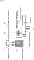
- apparatuses include an apparatus that can perform bubbling supply of a precursor as shown in Fig. 1 and an apparatus having a vaporization chamber as shown in Fig. 2 .
- an apparatus that can perform a plasma treatment on a reactive gas as shown in Fig. 3 and Fig. 4 may be exemplified.
- An apparatus that can simultaneously process a plurality of wafers using a batch furnace can be used without there being limitation to a single-wafer type apparatus as shown in Fig. 1 , Fig. 2 , Fig. 3 , and Fig. 4 .
- a titanium-atom-containing thin film manufactured using the raw materials for thin film formation of the present invention is used for a cutting tool, and wiring and electrodes for electronic goods, and can be used for, for example, a semiconductor memory material and an electrode for a lithium-air battery.
- the method of manufacturing a thin film of the present invention is a CVD method in which vapor obtained by vaporizing the compound represented by General Formula (1), and a reactive gas used as necessary are introduced into a film formation chamber in which a substrate is disposed, and next, a precursor decomposes and/or is chemically reacted, on the substrate and/or in the film formation chamber and/or near a gas inlet and a titanium-atom-containing thin film grows and is deposited on the surface of the substrate.
- a deposition method, manufacturing conditions, a manufacturing apparatus, and the like generally known conditions and methods can be used without any particular limitation.
- Examples of reactive gases used as necessary include oxygen, ozone, nitrogen dioxide, nitric oxide, water vapor, hydrogen peroxide, formic acid, acetic acid, and acetic anhydride which have oxidizability, and hydrogen, silane compounds such as monosilane and disilane, boron compounds such as diborane, and phosphorus compounds such as phosphine which have reducibility.
- examples of reactive gases that can produce a nitride include organic amine compounds such as monoalkylamines, dialkylamines, trialkylamines, and alkylenediamines, hydrazine, and ammonia, and these can be used alone or two or more types thereof can be used in combination.
- the reactive gas can be subjected to a plasma treatment before it reacts with a precursor.
- examples of delivery and feed methods include the gas delivery method, liquid delivery method, single source method, and cocktail source method described above.
- examples of the above deposition methods include thermal CVD in which a thin film is deposited by reacting a raw material gas or a raw material gas and a reactive gas only by heating, plasma CVD using heat and plasma, photo CVD using heat and light, light plasma CVD using heat, light and plasma, and ALD in which a CVD deposition reaction is divided into elementary processes and stepwise deposition is performed at the molecular level.
- Examples of materials of the above substrate include silicon; ceramics such as indium arsenide, indium gallium arsenide, silicon oxide, silicon nitride, silicon carbide, titanium nitride, tantalum oxide, tantalum nitride, titanium oxide, titanium nitride, ruthenium oxide, zirconium oxide, hafnium oxide, lanthanum oxide, and gallium nitride; glass; and metals such as platinum, ruthenium, aluminum, copper, nickel, cobalt, tungsten, and molybdenum.
- Examples of the form of the substrate include a plate shape, a spherical shape, a fibrous form, and a scaly shape.
- the surface of the substrate may be flat or may have a 3D structure such as a trench structure.
- the above manufacturing conditions include a reaction temperature (substrate temperature), a reaction pressure, a deposition rate, and the like.
- the reaction temperature is preferably 100°C or higher which is a temperature at which the compound represented by General Formula (1) sufficiently reacts, and more preferably 150°C to 400°C.
- the reaction pressure is preferably 10 Pa to atmospheric pressure in the case of thermal CVD or photo CVD, and is preferably 10 Pa to 2,000 Pa when a plasma is used.
- the deposition rate can be controlled according to raw material feed conditions (vaporization temperature, vaporization pressure), the reaction temperature, and the reaction pressure.
- the deposition rate is preferably 0.01 nm/min to 100 nm/min and more preferably 1 nm/min to 50 nm/min since characteristics of the obtained thin film may deteriorate if the deposition rate is high and problems may occur in productivity if the deposition rate is low.
- the number of cycles is controlled to obtain a desired film thickness.
- the above manufacturing conditions further include a temperature and pressure at which the raw material for thin film formation is vaporized into a vapor.
- a step of vaporizing the raw material for thin film formation into a vapor may be performed in the raw material container or in the vaporization chamber.
- the raw material for thin film formation used in the method for manufacturing a thin film of the present invention is preferably evaporated at 0°C to 150°C.
- the pressure in the raw material container and the pressure in the vaporization chamber are both preferably 1 Pa to 10,000 Pa.
- the method for manufacturing a thin film of the present invention adopts the ALD method, and may include, in addition to a step for introducing raw material in which a raw material for thin formation is vaporized into a vapor and the vapor is introduced into a film formation chamber according to the delivery and feed method, a step for forming precursor thin film in which a precursor thin film is formed on the surface of the substrate using the compound represented by General Formula (1) in the vapor, an exhaust step in which unreacted compound (represented by General Formula (1)) gases are exhausted, and a titanium-atom-containing thin film forming step in which the precursor thin film is chemically reacted with a reactive gas to form a titanium-atom-containing thin film on the surface of the substrate.
- a titanium-atom-containing thin film is formed by the ALD method as an example.
- the raw material introducing step described above is performed.
- a preferable temperature and pressure when the raw material for thin film formation is vaporized into a vapor are the same as those described above.
- a precursor thin film is formed on the surfaces of the substrate using the compound represented by General Formula (1) introduced into the film formation chamber (step for forming precursor thin film).
- the substrate may be heated or the film formation chamber may be heated to apply heat.
- the precursor thin film formed in this step is a thin film formed by adsorbing the compound represented by General Formula (1) on the surface of the substrate or formed by decomposition and/or reaction of the compound or a part of the compound, and has a composition different from a desired titanium-atom-containing thin film.
- the temperature of the substrate when this step is performed is preferably room temperature to 600°C and more preferably 150°C to 400°C.
- the pressure in the system (in the film formation chamber) when this step is performed is preferably 1 Pa to 10,000 Pa and more preferably 10 Pa to 1,000 Pa.
- unreacted compound (represented by General Formula (1)) gases and by-product gases are exhausted from the film formation chamber (exhaust step).
- Unreacted compound gases represented by General Formula (1) and by-product gases should ideally be completely exhausted from the film formation chamber, but they are not necessarily completely exhausted.
- Examples of an exhaust method include a method for purging the inside of the system with an inert gas such as nitrogen, helium, and argon, a method for exhausting by reducing the pressure in the system, and a combination method thereof.
- the degree of pressure reduction is preferably 0.01 Pa to 300 Pa, and more preferably 0.01 Pa to 100 Pa.
- a reactive gas is introduced into the film formation chamber, and a titanium-atom-containing thin film is formed from the precursor thin film obtained in the step for forming the previous precursor thin film by the action of the reactive gas or the action of the reactive gas and heat (step for forming titanium-atom-containing thin film) .
- the temperature when heat is applied in this step is preferably room temperature to 600°C and more preferably 150°C to 400°C.
- the pressure in the system (in the film formation chamber) when this step is performed is preferably 1 Pa to 10,000 Pa and more preferably 10 Pa to 1,000 Pa.
- thin film deposition according to a series of operations including the above raw material introducing step, precursor thin film forming step, exhaust step, and step for forming titanium-atom-containing thin film is set as one cycle, and this cycle may be repeated a plurality of times until a thin film with a required film thickness is obtained.
- this cycle may be repeated a plurality of times until a thin film with a required film thickness is obtained.
- unreacted compound (represented by General Formula (1)) gases and a reactive gas, and additionally by-product gases are exhausted from the film formation chamber, and the next one cycle is then performed.
- a time for which the energy is applied is not particularly limited, and the time may be, for example, during introducing a compound gas in the step for introducing raw material, during heating in the step for forming a precursor thin film or in the step for forming titanium-atom-containing thin film, during exhausting in the system in the exhaust step, during introduction of a reactive gas in the step for forming titanium-atom-containing thin film, or may be between the steps.
- energy can be applied to a reactive gas before the reactive gas is introduced.
- the reactive gas may continue to flow into the film formation chamber during all steps in the manufacturing method, or a reactive gas treated with plasma may be introduced into the film formation chamber only in the step for forming a titanium-atom-containing thin film.
- the high frequency (hereinafter referred to as an RF) output is too low, it is difficult to form a favorable film containing titanium atoms, and if the high frequency output is too high, damage to the substrate is too large. Therefore, the output is preferably 0 to 1,500 W and more preferably 50 W to 600 W.
- a plasma ALD method is preferably used since a titanium-atom-containing thin film with very high quality can be obtained.
- an annealing treatment may be performed under an inert atmosphere, or a reflow step may be provided when step coverage is necessary.
- the temperature in this case is 200°C to 1,000°C and preferably 250°C to 500°C.
- the compound represented by General Formula (2) is novel as a compound.
- the novel compound of the present invention has a low melting point, and can be applied in an ALD method, and is a compound particularly suitable as a precursor for a method for manufacturing thin film including a vaporization step such as the CVD method.
- L represents a primary alkyl group having 2 to 5 carbon atoms or a secondary butyl group.
- a primary alkyl group having 2 to 5 carbon atoms include an ethyl group, an n-propyl group, an n-butyl group, and an n-pentyl group.
- L is preferably an ethyl group since the melting point is particularly low.
- the compound represented by General Formula (2) is not particularly limited by the method for manufacturing and is manufactured by applying a known reaction.
- a manufacturing method for example, when L is an ethyl group, the compound can be obtained by reacting titanium tetrabromide with trimethyl(3-ethyl-2,4-cyclopentadien-1-yl) silane at room temperature, and performing distillation and purification.
- L is a propyl group
- the compound can be obtained by reacting titanium tetrabromide with trimethyl(3-propyl-2,4-cyclopentadien-1-yl) silane at room temperature and performing distillation and purification.
- L is a butyl group
- the compound can be obtained by reacting titanium tetrabromide with trimethyl(3-butyl-2,4-cyclopentadien-1-yl) silane at room temperature and performing distillation and purification.
- novel compound represented by General Formula (2) include, for example, compounds represented as Compounds Nos. 8 to 12.
- Compound No. 3 was used as a raw material for an ALD method, and a titanium carbide thin film was manufactured on a silicon wafer using the apparatus shown in Fig. 3 by the ALD method under the following conditions.
- the film thickness of the obtained thin film was measured according to an X-ray reflectance method, and the thin film structure and the thin film composition were checked using an X-ray diffraction method and X-ray photoelectron spectroscopy.
- the film thickness was 7.6 nm
- the film composition was a titanium carbide thin film
- the carbon content was 51 atom% (theoretical amount of 50 atom%).
- the residual carbon components as organic substances were not detected.
- the film thickness obtained for one cycle was 0.15 nm.
- Reaction temperature (substrate temperature): 250°C
- reactive gas hydrogen
- steps A series of steps including the following (1) to (4) was set as one cycle and repeated over 50 cycles.
- a titanium carbide thin film was produced under the same conditions as in Example 3 except that Compound No. 4 was used as a raw material for an ALD method.
- the film thickness of the obtained thin film was measured according to an X-ray reflectance method, and the thin film structure and the thin film composition were checked using an X-ray diffraction method and X-ray photoelectron spectroscopy.
- the film thickness was 7.5 nm
- the film composition was a titanium carbide thin film
- the carbon content was 52 atom% (theoretical amount of 50 atom%). Residual carbon components as organic substances were not detected.
- the film thickness obtained for one cycle was 0.15 nm.
- a titanium carbide thin film was manufactured under the same conditions as in Example 3 except that Compound No. 5 was used as a raw material for an ALD method.
- the film thickness of the obtained thin film was measured according to an X-ray reflectance method, and the thin film structure and the thin film composition were checked using an X-ray diffraction method and X-ray photoelectron spectroscopy.
- the film thickness was 7.8 nm
- the film composition was a titanium carbide thin film
- the carbon content was 52 atom% (theoretical amount of 50 atom%). Residual carbon components as organic substances were not detected.
- the film thickness obtained for one cycle was 0.16 nm.
- a titanium carbide thin film was manufactured under the same conditions as in Example 3 except that Compound No. 8 was used as a raw material for an ALD method.
- the film thickness of the obtained thin film was measured according to an X-ray reflectance method, and the thin film structure and the thin film composition were checked using an X-ray diffraction method and X-ray photoelectron spectroscopy.
- the film thickness was 7.2 nm
- the film composition was a titanium carbide thin film
- the carbon content was 50 atom% (theoretical amount of 50 atom%). Residual carbon components as organic substances were not detected.
- the film thickness obtained for one cycle was 0.14 nm.
- a titanium carbide thin film was manufactured under the same conditions as in Example 3 except that Compound No. 10 was used as a raw material for an ALD method.
- the film thickness of the obtained thin film was measured according to an X-ray reflectance method, and the thin film structure and the thin film composition were checked using an X-ray diffraction method and X-ray photoelectron spectroscopy.
- the film thickness was 7.0 nm
- the film composition was a titanium carbide thin film
- the carbon content was 51 atom% (theoretical amount of 50 atom%). Residual carbon components as organic substances were not detected.
- the film thickness obtained for one cycle was 0.14 nm.
- a titanium carbide thin film was manufactured under the same conditions as in Example 1 except that tetrakis neopentyl titanium was used as a raw material for an ALD method.
- the film thickness of the obtained thin film was measured according to an X-ray reflectance method, and the thin film structure and the thin film composition were checked using an X-ray diffraction method and X-ray photoelectron spectroscopy.
- the film thickness was 1.0 nm
- the film composition was titanium carbide
- the carbon content was 40 atom% (theoretical amount of 50 atom%) .
- 10 atom% or more of residual carbon components as organic substances were detected.
- the film thickness obtained for one cycle was 0.12 nm.
Landscapes
- Chemical & Material Sciences (AREA)
- Organic Chemistry (AREA)
- Engineering & Computer Science (AREA)
- Chemical Kinetics & Catalysis (AREA)
- General Chemical & Material Sciences (AREA)
- Materials Engineering (AREA)
- Mechanical Engineering (AREA)
- Metallurgy (AREA)
- Inorganic Chemistry (AREA)
- Physics & Mathematics (AREA)
- Electromagnetism (AREA)
- Plasma & Fusion (AREA)
- Chemical Vapour Deposition (AREA)
- Electrodes Of Semiconductors (AREA)
- Oxygen, Ozone, And Oxides In General (AREA)
- Inorganic Compounds Of Heavy Metals (AREA)
- Formation Of Insulating Films (AREA)
Claims (7)
- Utilisation d'une matière première pour la formation d'un film mince contenant un composé représenté par la Formule Générale (1) :

- Utilisation selon la revendication 1, dans laquelle X est un atome de chlore ou un atome de brome.
- Utilisation selon la revendication 1 ou 2, dans laquelle X est un atome de chlore, et R est un groupe alkyle primaire ayant 3 à 5 atomes de carbone ou un groupe butyle secondaire.
- Utilisation selon la revendication 1 ou 2, dans laquelle X est un atome de brome, et R est un groupe alkyle primaire ayant 2 à 4 atomes de carbone ou un groupe butyle secondaire.
- Procédé de fabrication d'un film mince contenant des atomes de titane, comprenant :la vaporisation de la matière première pour la formation d'un film mince telle que définie dans l'une quelconque des revendications 1 à 4 ;l'introduction de la vapeur résultante contenant le composé représenté par la Formule Générale (1) dans une atmosphère de traitement ; etla décomposition et/ou la mise en réaction chimique du composé et la réalisation d'un dépôt sur une surface d'un substrat.
- Composé représenté par la Formule Générale (2) suivante :

- Composé selon la revendication 6, dans lequel L est un groupe éthyle.
Applications Claiming Priority (2)
| Application Number | Priority Date | Filing Date | Title |
|---|---|---|---|
| JP2017127401A JP6954776B2 (ja) | 2017-06-29 | 2017-06-29 | 薄膜形成用原料及び薄膜の製造方法 |
| PCT/JP2018/019080 WO2019003695A1 (fr) | 2017-06-29 | 2018-05-17 | Charge d'alimentation pour la formation de films minces, procédé de production de films minces et nouveau composé |
Publications (3)
| Publication Number | Publication Date |
|---|---|
| EP3647460A1 EP3647460A1 (fr) | 2020-05-06 |
| EP3647460A4 EP3647460A4 (fr) | 2021-04-14 |
| EP3647460B1 true EP3647460B1 (fr) | 2023-04-12 |
Family
ID=64740523
Family Applications (1)
| Application Number | Title | Priority Date | Filing Date |
|---|---|---|---|
| EP18823105.4A Active EP3647460B1 (fr) | 2017-06-29 | 2018-05-17 | Procédé de production de films minces et nouveau composé |
Country Status (8)
| Country | Link |
|---|---|
| US (1) | US20200131042A1 (fr) |
| EP (1) | EP3647460B1 (fr) |
| JP (1) | JP6954776B2 (fr) |
| KR (1) | KR102602822B1 (fr) |
| CN (1) | CN110799665B (fr) |
| IL (1) | IL271542B2 (fr) |
| TW (1) | TWI805584B (fr) |
| WO (1) | WO2019003695A1 (fr) |
Citations (1)
| Publication number | Priority date | Publication date | Assignee | Title |
|---|---|---|---|---|
| US20140134331A1 (en) * | 2011-07-21 | 2014-05-15 | Jsr Corporation | Method for producing substrate with metal body |
Family Cites Families (17)
| Publication number | Priority date | Publication date | Assignee | Title |
|---|---|---|---|---|
| JPH06145987A (ja) * | 1992-09-18 | 1994-05-27 | Sharp Corp | チタン系膜の形成方法 |
| US6197683B1 (en) * | 1997-09-29 | 2001-03-06 | Samsung Electronics Co., Ltd. | Method of forming metal nitride film by chemical vapor deposition and method of forming metal contact of semiconductor device using the same |
| KR100304694B1 (ko) * | 1997-09-29 | 2001-11-02 | 윤종용 | 화학기상증착법에의한금속질화막형성방법및이를이용한반도체장치의금속컨택형성방법 |
| JP2000154210A (ja) * | 1998-09-15 | 2000-06-06 | Agency Of Ind Science & Technol | 共役ジエン重合用触媒、共役ジエン系重合体の製造方法、イソプレン系重合体およびブタジエン系共重合体 |
| JP4110973B2 (ja) * | 2003-01-17 | 2008-07-02 | Jsr株式会社 | シリコン−アルミニウム混合膜形成用組成物、シリコン−アルミニウム混合膜およびその形成方法 |
| JP3910166B2 (ja) * | 2003-09-09 | 2007-04-25 | 独立行政法人科学技術振興機構 | チタノセン類を触媒とする芳香族フッ素化物の脱フッ素化処理方法 |
| CN1289541C (zh) * | 2004-06-04 | 2006-12-13 | 中国石油化工股份有限公司 | 含单茂、单齿大位阻非茂混合配体钛催化剂及制备和应用 |
| US7514119B2 (en) | 2005-04-29 | 2009-04-07 | Linde, Inc. | Method and apparatus for using solution based precursors for atomic layer deposition |
| US20100036144A1 (en) | 2006-07-20 | 2010-02-11 | Ce Ma | Methods for atomic layer deposition |
| JP5424715B2 (ja) * | 2008-06-23 | 2014-02-26 | 東ソー株式会社 | チタン錯体、その製造方法、チタン含有薄膜及びその製法 |
| JP2010189385A (ja) * | 2009-01-26 | 2010-09-02 | Koei Chem Co Ltd | シクロペンタジエン類の製造方法 |
| US8765220B2 (en) | 2009-11-09 | 2014-07-01 | American Air Liquide, Inc. | Methods of making and deposition methods using hafnium- or zirconium-containing compounds |
| CN103930431B (zh) * | 2011-03-15 | 2016-07-06 | 株式会社Mecharonics | 新型第4b族金属有机化合物及其制备 |
| US20120308739A1 (en) * | 2011-05-30 | 2012-12-06 | L'air Liquide Societe Anonyme Pour I'etude Et I'exploitation Des Procedes Georges Claude | Methods for deposition of alkaline earth metal fluoride films |
| EP2754638B1 (fr) * | 2011-09-05 | 2018-11-07 | Tosoh Corporation | Matière filmogène, film d'oxyde d'un métal du groupe iv et complexe vinylène diamide |
| JP5352024B1 (ja) * | 2013-05-22 | 2013-11-27 | 田中貴金属工業株式会社 | 有機ニッケル化合物からなる化学蒸着用原料及び該化学蒸着用原料を用いた化学蒸着法 |
| TWI664185B (zh) * | 2013-12-22 | 2019-07-01 | 美商恩特葛瑞斯股份有限公司 | 具有用於TiO原子層沉積的臭氧活化配位基之環戊二烯鈦醇鹽 |
-
2017
- 2017-06-29 JP JP2017127401A patent/JP6954776B2/ja active Active
-
2018
- 2018-05-17 EP EP18823105.4A patent/EP3647460B1/fr active Active
- 2018-05-17 WO PCT/JP2018/019080 patent/WO2019003695A1/fr not_active Ceased
- 2018-05-17 US US16/624,433 patent/US20200131042A1/en not_active Abandoned
- 2018-05-17 CN CN201880043465.1A patent/CN110799665B/zh active Active
- 2018-05-17 KR KR1020207002315A patent/KR102602822B1/ko active Active
- 2018-05-30 TW TW107118428A patent/TWI805584B/zh active
-
2019
- 2019-12-18 IL IL271542A patent/IL271542B2/en unknown
Patent Citations (1)
| Publication number | Priority date | Publication date | Assignee | Title |
|---|---|---|---|---|
| US20140134331A1 (en) * | 2011-07-21 | 2014-05-15 | Jsr Corporation | Method for producing substrate with metal body |
Also Published As
| Publication number | Publication date |
|---|---|
| CN110799665B (zh) | 2025-10-24 |
| JP2019011490A (ja) | 2019-01-24 |
| TW201923133A (zh) | 2019-06-16 |
| WO2019003695A1 (fr) | 2019-01-03 |
| KR20200024851A (ko) | 2020-03-09 |
| US20200131042A1 (en) | 2020-04-30 |
| JP6954776B2 (ja) | 2021-10-27 |
| EP3647460A1 (fr) | 2020-05-06 |
| IL271542B2 (en) | 2023-07-01 |
| TWI805584B (zh) | 2023-06-21 |
| EP3647460A4 (fr) | 2021-04-14 |
| CN110799665A (zh) | 2020-02-14 |
| IL271542A (en) | 2020-02-27 |
| KR102602822B1 (ko) | 2023-11-15 |
| IL271542B1 (en) | 2023-03-01 |
Similar Documents
| Publication | Publication Date | Title |
|---|---|---|
| JP5843318B2 (ja) | Ald法用窒化アルミニウム系薄膜形成用原料及び該薄膜の製造方法 | |
| EP3783130A1 (fr) | Matériau source de formation de film mince de dépôt de couche atomique et procédé de production d'un film mince | |
| EP3677585A1 (fr) | Composé alcoxyde métallique, matière première de formation de film mince, et procédé de production de film mince | |
| EP3712159B1 (fr) | Composé ruthénium, matière de départ pour formation de film mince, et procédé de fabrication de film mince | |
| JP7717051B2 (ja) | 原子層堆積法用薄膜形成用原料及び薄膜の製造方法 | |
| WO2022190877A1 (fr) | Matériau de départ formant un film mince, destiné à être utilisé dans un procédé de dépôt de couche atomique, film mince, procédé de production de film mince et composé de zinc | |
| KR102952121B1 (ko) | 신규 화합물, 그 화합물을 함유하는 박막 형성용 원료 및 박막의 제조 방법 | |
| JP7592611B2 (ja) | 新規スズ化合物、該化合物を含有する薄膜形成用原料、該薄膜形成用原料を用いて形成される薄膜、該薄膜を製造するために該化合物をプリカーサとして用いる方法、及び該薄膜の製造方法 | |
| EP3643700A1 (fr) | Composé alcoxyde métallique, matière première de formation de couche mince, et procédé de production de couche mince | |
| JP6691009B2 (ja) | 金属炭化物含有薄膜形成用原料及び金属炭化物含有薄膜の製造方法 | |
| JP7796014B2 (ja) | 薄膜形成用原料、薄膜及び薄膜の製造方法 | |
| KR102875898B1 (ko) | 아연 화합물, 박막 형성용 원료, 박막 및 그 제조 방법 | |
| KR102822492B1 (ko) | 화합물, 박막 형성용 원료 및 박막의 제조 방법 | |
| JP7636336B2 (ja) | 酸化イットリウム含有膜の製造方法 | |
| JP2025081785A (ja) | 原子層堆積法用薄膜形成用原料、薄膜及び薄膜の製造方法 | |
| JP6704808B2 (ja) | 薄膜形成用原料及び薄膜の製造方法 | |
| EP3647460A1 (fr) | Charge d'alimentation pour la formation de films minces, procédé de production de films minces et nouveau composé | |
| WO2021054160A1 (fr) | Matière première de formation de film mince pour dépôt de couches atomiques et procédé de production d'un film mince contenant du zinc et utilisant cette matière première | |
| JP7758681B2 (ja) | 原子層堆積法用薄膜形成原料及び薄膜の製造方法 | |
| KR20250155913A (ko) | 박막 형성용 조성물, 박막 형성용 조성물의 제조 방법, 박막 및 박막의 제조 방법 | |
| KR20260019524A (ko) | 화합물, 박막 형성용 원료, 박막 및 박막의 제조 방법 | |
| WO2023090179A1 (fr) | Matériau de formation de film mince destiné à être utilisé dans le dépôt de couche atomique, film mince, procédé de production de film mince et composé de ruthénium | |
| KR20250142364A (ko) | 화합물, 박막 형성용 원료, 박막 및 박막의 제조 방법 | |
| WO2023276716A1 (fr) | Produit de départ pour former un film mince, film mince et procédé de production de film mince | |
| WO2022107769A1 (fr) | Procédé de fabrication de couche mince |
Legal Events
| Date | Code | Title | Description |
|---|---|---|---|
| STAA | Information on the status of an ep patent application or granted ep patent |
Free format text: STATUS: THE INTERNATIONAL PUBLICATION HAS BEEN MADE |
|
| PUAI | Public reference made under article 153(3) epc to a published international application that has entered the european phase |
Free format text: ORIGINAL CODE: 0009012 |
|
| STAA | Information on the status of an ep patent application or granted ep patent |
Free format text: STATUS: REQUEST FOR EXAMINATION WAS MADE |
|
| 17P | Request for examination filed |
Effective date: 20191213 |
|
| AK | Designated contracting states |
Kind code of ref document: A1 Designated state(s): AL AT BE BG CH CY CZ DE DK EE ES FI FR GB GR HR HU IE IS IT LI LT LU LV MC MK MT NL NO PL PT RO RS SE SI SK SM TR |
|
| AX | Request for extension of the european patent |
Extension state: BA ME |
|
| DAV | Request for validation of the european patent (deleted) | ||
| DAX | Request for extension of the european patent (deleted) | ||
| RIN1 | Information on inventor provided before grant (corrected) |
Inventor name: OKADA, NANA Inventor name: NISHIDA, AKIHIRO Inventor name: OOE, YOSHIKI |
|
| A4 | Supplementary search report drawn up and despatched |
Effective date: 20210315 |
|
| RIC1 | Information provided on ipc code assigned before grant |
Ipc: C23C 16/32 20060101AFI20210309BHEP Ipc: C07F 17/00 20060101ALI20210309BHEP Ipc: H01L 21/316 20060101ALI20210309BHEP Ipc: C07F 7/28 20060101ALI20210309BHEP Ipc: C23C 16/455 20060101ALI20210309BHEP |
|
| RIC1 | Information provided on ipc code assigned before grant |
Ipc: H01L 21/316 20060101ALI20220531BHEP Ipc: C07F 7/28 20060101ALI20220531BHEP Ipc: C07F 17/00 20060101ALI20220531BHEP Ipc: C23C 16/455 20060101ALI20220531BHEP Ipc: C23C 16/32 20060101AFI20220531BHEP |
|
| GRAP | Despatch of communication of intention to grant a patent |
Free format text: ORIGINAL CODE: EPIDOSNIGR1 |
|
| STAA | Information on the status of an ep patent application or granted ep patent |
Free format text: STATUS: GRANT OF PATENT IS INTENDED |
|
| RIC1 | Information provided on ipc code assigned before grant |
Ipc: H01L 21/316 20060101ALI20220627BHEP Ipc: C07F 17/00 20060101ALI20220627BHEP Ipc: C23C 16/455 20060101ALI20220627BHEP Ipc: C23C 16/32 20060101AFI20220627BHEP |
|
| INTG | Intention to grant announced |
Effective date: 20220713 |
|
| GRAJ | Information related to disapproval of communication of intention to grant by the applicant or resumption of examination proceedings by the epo deleted |
Free format text: ORIGINAL CODE: EPIDOSDIGR1 |
|
| STAA | Information on the status of an ep patent application or granted ep patent |
Free format text: STATUS: REQUEST FOR EXAMINATION WAS MADE |
|
| INTC | Intention to grant announced (deleted) | ||
| GRAS | Grant fee paid |
Free format text: ORIGINAL CODE: EPIDOSNIGR3 |
|
| STAA | Information on the status of an ep patent application or granted ep patent |
Free format text: STATUS: GRANT OF PATENT IS INTENDED |
|
| GRAP | Despatch of communication of intention to grant a patent |
Free format text: ORIGINAL CODE: EPIDOSNIGR1 |
|
| RIC1 | Information provided on ipc code assigned before grant |
Ipc: C23C 16/455 20060101ALI20221128BHEP Ipc: C23C 16/32 20060101AFI20221128BHEP |
|
| INTG | Intention to grant announced |
Effective date: 20221222 |
|
| GRAA | (expected) grant |
Free format text: ORIGINAL CODE: 0009210 |
|
| STAA | Information on the status of an ep patent application or granted ep patent |
Free format text: STATUS: THE PATENT HAS BEEN GRANTED |
|
| AK | Designated contracting states |
Kind code of ref document: B1 Designated state(s): AL AT BE BG CH CY CZ DE DK EE ES FI FR GB GR HR HU IE IS IT LI LT LU LV MC MK MT NL NO PL PT RO RS SE SI SK SM TR |
|
| REG | Reference to a national code |
Ref country code: GB Ref legal event code: FG4D |
|
| REG | Reference to a national code |
Ref country code: CH Ref legal event code: EP |
|
| REG | Reference to a national code |
Ref country code: DE Ref legal event code: R096 Ref document number: 602018048384 Country of ref document: DE |
|
| REG | Reference to a national code |
Ref country code: IE Ref legal event code: FG4D |
|
| REG | Reference to a national code |
Ref country code: AT Ref legal event code: REF Ref document number: 1559835 Country of ref document: AT Kind code of ref document: T Effective date: 20230515 |
|
| P01 | Opt-out of the competence of the unified patent court (upc) registered |
Effective date: 20230530 |
|
| REG | Reference to a national code |
Ref country code: LT Ref legal event code: MG9D |
|
| REG | Reference to a national code |
Ref country code: NL Ref legal event code: MP Effective date: 20230412 |
|
| REG | Reference to a national code |
Ref country code: AT Ref legal event code: MK05 Ref document number: 1559835 Country of ref document: AT Kind code of ref document: T Effective date: 20230412 |
|
| PG25 | Lapsed in a contracting state [announced via postgrant information from national office to epo] |
Ref country code: NL Free format text: LAPSE BECAUSE OF FAILURE TO SUBMIT A TRANSLATION OF THE DESCRIPTION OR TO PAY THE FEE WITHIN THE PRESCRIBED TIME-LIMIT Effective date: 20230412 |
|
| PG25 | Lapsed in a contracting state [announced via postgrant information from national office to epo] |
Ref country code: SE Free format text: LAPSE BECAUSE OF FAILURE TO SUBMIT A TRANSLATION OF THE DESCRIPTION OR TO PAY THE FEE WITHIN THE PRESCRIBED TIME-LIMIT Effective date: 20230412 Ref country code: PT Free format text: LAPSE BECAUSE OF FAILURE TO SUBMIT A TRANSLATION OF THE DESCRIPTION OR TO PAY THE FEE WITHIN THE PRESCRIBED TIME-LIMIT Effective date: 20230814 Ref country code: NO Free format text: LAPSE BECAUSE OF FAILURE TO SUBMIT A TRANSLATION OF THE DESCRIPTION OR TO PAY THE FEE WITHIN THE PRESCRIBED TIME-LIMIT Effective date: 20230712 Ref country code: ES Free format text: LAPSE BECAUSE OF FAILURE TO SUBMIT A TRANSLATION OF THE DESCRIPTION OR TO PAY THE FEE WITHIN THE PRESCRIBED TIME-LIMIT Effective date: 20230412 Ref country code: AT Free format text: LAPSE BECAUSE OF FAILURE TO SUBMIT A TRANSLATION OF THE DESCRIPTION OR TO PAY THE FEE WITHIN THE PRESCRIBED TIME-LIMIT Effective date: 20230412 |
|
| PG25 | Lapsed in a contracting state [announced via postgrant information from national office to epo] |
Ref country code: RS Free format text: LAPSE BECAUSE OF FAILURE TO SUBMIT A TRANSLATION OF THE DESCRIPTION OR TO PAY THE FEE WITHIN THE PRESCRIBED TIME-LIMIT Effective date: 20230412 Ref country code: PL Free format text: LAPSE BECAUSE OF FAILURE TO SUBMIT A TRANSLATION OF THE DESCRIPTION OR TO PAY THE FEE WITHIN THE PRESCRIBED TIME-LIMIT Effective date: 20230412 Ref country code: LV Free format text: LAPSE BECAUSE OF FAILURE TO SUBMIT A TRANSLATION OF THE DESCRIPTION OR TO PAY THE FEE WITHIN THE PRESCRIBED TIME-LIMIT Effective date: 20230412 Ref country code: LT Free format text: LAPSE BECAUSE OF FAILURE TO SUBMIT A TRANSLATION OF THE DESCRIPTION OR TO PAY THE FEE WITHIN THE PRESCRIBED TIME-LIMIT Effective date: 20230412 Ref country code: IS Free format text: LAPSE BECAUSE OF FAILURE TO SUBMIT A TRANSLATION OF THE DESCRIPTION OR TO PAY THE FEE WITHIN THE PRESCRIBED TIME-LIMIT Effective date: 20230812 Ref country code: HR Free format text: LAPSE BECAUSE OF FAILURE TO SUBMIT A TRANSLATION OF THE DESCRIPTION OR TO PAY THE FEE WITHIN THE PRESCRIBED TIME-LIMIT Effective date: 20230412 Ref country code: GR Free format text: LAPSE BECAUSE OF FAILURE TO SUBMIT A TRANSLATION OF THE DESCRIPTION OR TO PAY THE FEE WITHIN THE PRESCRIBED TIME-LIMIT Effective date: 20230713 Ref country code: AL Free format text: LAPSE BECAUSE OF FAILURE TO SUBMIT A TRANSLATION OF THE DESCRIPTION OR TO PAY THE FEE WITHIN THE PRESCRIBED TIME-LIMIT Effective date: 20230412 |
|
| REG | Reference to a national code |
Ref country code: DE Ref legal event code: R119 Ref document number: 602018048384 Country of ref document: DE |
|
| PG25 | Lapsed in a contracting state [announced via postgrant information from national office to epo] |
Ref country code: FI Free format text: LAPSE BECAUSE OF FAILURE TO SUBMIT A TRANSLATION OF THE DESCRIPTION OR TO PAY THE FEE WITHIN THE PRESCRIBED TIME-LIMIT Effective date: 20230412 |
|
| REG | Reference to a national code |
Ref country code: CH Ref legal event code: PL |
|
| PG25 | Lapsed in a contracting state [announced via postgrant information from national office to epo] |
Ref country code: SK Free format text: LAPSE BECAUSE OF FAILURE TO SUBMIT A TRANSLATION OF THE DESCRIPTION OR TO PAY THE FEE WITHIN THE PRESCRIBED TIME-LIMIT Effective date: 20230412 |
|
| PG25 | Lapsed in a contracting state [announced via postgrant information from national office to epo] |
Ref country code: MC Free format text: LAPSE BECAUSE OF FAILURE TO SUBMIT A TRANSLATION OF THE DESCRIPTION OR TO PAY THE FEE WITHIN THE PRESCRIBED TIME-LIMIT Effective date: 20230412 |
|
| REG | Reference to a national code |
Ref country code: BE Ref legal event code: MM Effective date: 20230531 |
|
| PG25 | Lapsed in a contracting state [announced via postgrant information from national office to epo] |
Ref country code: SM Free format text: LAPSE BECAUSE OF FAILURE TO SUBMIT A TRANSLATION OF THE DESCRIPTION OR TO PAY THE FEE WITHIN THE PRESCRIBED TIME-LIMIT Effective date: 20230412 Ref country code: SK Free format text: LAPSE BECAUSE OF FAILURE TO SUBMIT A TRANSLATION OF THE DESCRIPTION OR TO PAY THE FEE WITHIN THE PRESCRIBED TIME-LIMIT Effective date: 20230412 Ref country code: RO Free format text: LAPSE BECAUSE OF FAILURE TO SUBMIT A TRANSLATION OF THE DESCRIPTION OR TO PAY THE FEE WITHIN THE PRESCRIBED TIME-LIMIT Effective date: 20230412 Ref country code: MC Free format text: LAPSE BECAUSE OF FAILURE TO SUBMIT A TRANSLATION OF THE DESCRIPTION OR TO PAY THE FEE WITHIN THE PRESCRIBED TIME-LIMIT Effective date: 20230412 Ref country code: LU Free format text: LAPSE BECAUSE OF NON-PAYMENT OF DUE FEES Effective date: 20230517 Ref country code: LI Free format text: LAPSE BECAUSE OF NON-PAYMENT OF DUE FEES Effective date: 20230531 Ref country code: EE Free format text: LAPSE BECAUSE OF FAILURE TO SUBMIT A TRANSLATION OF THE DESCRIPTION OR TO PAY THE FEE WITHIN THE PRESCRIBED TIME-LIMIT Effective date: 20230412 Ref country code: DK Free format text: LAPSE BECAUSE OF FAILURE TO SUBMIT A TRANSLATION OF THE DESCRIPTION OR TO PAY THE FEE WITHIN THE PRESCRIBED TIME-LIMIT Effective date: 20230412 Ref country code: CZ Free format text: LAPSE BECAUSE OF FAILURE TO SUBMIT A TRANSLATION OF THE DESCRIPTION OR TO PAY THE FEE WITHIN THE PRESCRIBED TIME-LIMIT Effective date: 20230412 Ref country code: CH Free format text: LAPSE BECAUSE OF NON-PAYMENT OF DUE FEES Effective date: 20230531 |
|
| PLBE | No opposition filed within time limit |
Free format text: ORIGINAL CODE: 0009261 |
|
| STAA | Information on the status of an ep patent application or granted ep patent |
Free format text: STATUS: NO OPPOSITION FILED WITHIN TIME LIMIT |
|
| 26N | No opposition filed |
Effective date: 20240115 |
|
| GBPC | Gb: european patent ceased through non-payment of renewal fee |
Effective date: 20230712 |
|
| PG25 | Lapsed in a contracting state [announced via postgrant information from national office to epo] |
Ref country code: DE Free format text: LAPSE BECAUSE OF NON-PAYMENT OF DUE FEES Effective date: 20231201 Ref country code: GB Free format text: LAPSE BECAUSE OF NON-PAYMENT OF DUE FEES Effective date: 20230712 |
|
| PG25 | Lapsed in a contracting state [announced via postgrant information from national office to epo] |
Ref country code: SI Free format text: LAPSE BECAUSE OF FAILURE TO SUBMIT A TRANSLATION OF THE DESCRIPTION OR TO PAY THE FEE WITHIN THE PRESCRIBED TIME-LIMIT Effective date: 20230412 |
|
| PG25 | Lapsed in a contracting state [announced via postgrant information from national office to epo] |
Ref country code: SI Free format text: LAPSE BECAUSE OF FAILURE TO SUBMIT A TRANSLATION OF THE DESCRIPTION OR TO PAY THE FEE WITHIN THE PRESCRIBED TIME-LIMIT Effective date: 20230412 Ref country code: IT Free format text: LAPSE BECAUSE OF FAILURE TO SUBMIT A TRANSLATION OF THE DESCRIPTION OR TO PAY THE FEE WITHIN THE PRESCRIBED TIME-LIMIT Effective date: 20230412 Ref country code: FR Free format text: LAPSE BECAUSE OF NON-PAYMENT OF DUE FEES Effective date: 20230612 Ref country code: BE Free format text: LAPSE BECAUSE OF NON-PAYMENT OF DUE FEES Effective date: 20230531 |
|
| PG25 | Lapsed in a contracting state [announced via postgrant information from national office to epo] |
Ref country code: BG Free format text: LAPSE BECAUSE OF FAILURE TO SUBMIT A TRANSLATION OF THE DESCRIPTION OR TO PAY THE FEE WITHIN THE PRESCRIBED TIME-LIMIT Effective date: 20230412 |
|
| PG25 | Lapsed in a contracting state [announced via postgrant information from national office to epo] |
Ref country code: BG Free format text: LAPSE BECAUSE OF FAILURE TO SUBMIT A TRANSLATION OF THE DESCRIPTION OR TO PAY THE FEE WITHIN THE PRESCRIBED TIME-LIMIT Effective date: 20230412 |
|
| PG25 | Lapsed in a contracting state [announced via postgrant information from national office to epo] |
Ref country code: CY Free format text: LAPSE BECAUSE OF FAILURE TO SUBMIT A TRANSLATION OF THE DESCRIPTION OR TO PAY THE FEE WITHIN THE PRESCRIBED TIME-LIMIT; INVALID AB INITIO Effective date: 20180517 |
|
| PGFP | Annual fee paid to national office [announced via postgrant information from national office to epo] |
Ref country code: IE Payment date: 20250521 Year of fee payment: 8 |
|
| PG25 | Lapsed in a contracting state [announced via postgrant information from national office to epo] |
Ref country code: HU Free format text: LAPSE BECAUSE OF FAILURE TO SUBMIT A TRANSLATION OF THE DESCRIPTION OR TO PAY THE FEE WITHIN THE PRESCRIBED TIME-LIMIT; INVALID AB INITIO Effective date: 20180517 |
|
| PG25 | Lapsed in a contracting state [announced via postgrant information from national office to epo] |
Ref country code: TR Free format text: LAPSE BECAUSE OF FAILURE TO SUBMIT A TRANSLATION OF THE DESCRIPTION OR TO PAY THE FEE WITHIN THE PRESCRIBED TIME-LIMIT Effective date: 20230412 |