EP3651385A1 - Circuit de commande pour supprimer des signaux d'interférence électromagnétique - Google Patents
Circuit de commande pour supprimer des signaux d'interférence électromagnétique Download PDFInfo
- Publication number
- EP3651385A1 EP3651385A1 EP19208121.4A EP19208121A EP3651385A1 EP 3651385 A1 EP3651385 A1 EP 3651385A1 EP 19208121 A EP19208121 A EP 19208121A EP 3651385 A1 EP3651385 A1 EP 3651385A1
- Authority
- EP
- European Patent Office
- Prior art keywords
- circuit
- signal
- control circuit
- electromagnetic interference
- output
- Prior art date
- Legal status (The legal status is an assumption and is not a legal conclusion. Google has not performed a legal analysis and makes no representation as to the accuracy of the status listed.)
- Granted
Links
Images


Classifications
-
- H—ELECTRICITY
- H03—ELECTRONIC CIRCUITRY
- H03H—IMPEDANCE NETWORKS, e.g. RESONANT CIRCUITS; RESONATORS
- H03H11/00—Networks using active elements
- H03H11/02—Multiple-port networks
- H03H11/04—Frequency selective two-port networks
- H03H11/12—Frequency selective two-port networks using amplifiers with feedback
- H03H11/126—Frequency selective two-port networks using amplifiers with feedback using a single operational amplifier
-
- H—ELECTRICITY
- H02—GENERATION; CONVERSION OR DISTRIBUTION OF ELECTRIC POWER
- H02M—APPARATUS FOR CONVERSION BETWEEN AC AND AC, BETWEEN AC AND DC, OR BETWEEN DC AND DC, AND FOR USE WITH MAINS OR SIMILAR POWER SUPPLY SYSTEMS; CONVERSION OF DC OR AC INPUT POWER INTO SURGE OUTPUT POWER; CONTROL OR REGULATION THEREOF
- H02M1/00—Details of apparatus for conversion
- H02M1/44—Circuits or arrangements for compensating for electromagnetic interference in converters or inverters
-
- H—ELECTRICITY
- H03—ELECTRONIC CIRCUITRY
- H03H—IMPEDANCE NETWORKS, e.g. RESONANT CIRCUITS; RESONATORS
- H03H11/00—Networks using active elements
- H03H11/02—Multiple-port networks
- H03H11/04—Frequency selective two-port networks
- H03H11/12—Frequency selective two-port networks using amplifiers with feedback
- H03H11/1291—Current or voltage controlled filters
-
- H—ELECTRICITY
- H04—ELECTRIC COMMUNICATION TECHNIQUE
- H04B—TRANSMISSION
- H04B15/00—Suppression or limitation of noise or interference
-
- H—ELECTRICITY
- H03—ELECTRONIC CIRCUITRY
- H03H—IMPEDANCE NETWORKS, e.g. RESONANT CIRCUITS; RESONATORS
- H03H2210/00—Indexing scheme relating to details of tunable filters
- H03H2210/02—Variable filter component
- H03H2210/025—Capacitor
-
- H—ELECTRICITY
- H03—ELECTRONIC CIRCUITRY
- H03H—IMPEDANCE NETWORKS, e.g. RESONANT CIRCUITS; RESONATORS
- H03H2210/00—Indexing scheme relating to details of tunable filters
- H03H2210/02—Variable filter component
- H03H2210/028—Resistor
Definitions
- the invention relates to suppression of electromagnetic interference signals conducted in signal or power lines in electric circuits.
- Electromagnetic interference suppression circuits are known and are commonly used for suppressing conducted electromagnetic interference signals present on a signal or power line. These conducted electromagnetic interference signals can be classified into differential mode electromagnetic interference signals, which are conducted on the power supply line and the power return line in opposite directions, and common mode electromagnetic interference signals, which are conducted on the power supply line and the power return line in the same direction.
- an electromagnetic interference suppression circuit is able to generate a suppression signal that can reduce or even eliminate the unwanted electromagnetic interference signal.
- the generated suppression signal should be a negative of the electromagnetic interference signal (e.g., equal in magnitude and anti-phase) so that the two always completely cancel each other.
- a gain factor of the circuit has to be precisely controlled to be equal to unity to match the amplitude of the suppression signal with the amplitude of the electromagnetic interference signal. But such gain factor is affected by various factors including the environment in which the circuit is arranged, intrinsic parameters of components of the circuit, the deterioration of circuit components over time, the operation condition of the circuit, etc. These factors cause undesirable performance variation during production as well as throughout the operating life of the circuit.
- the suppression signal has to be precisely controlled to be about 180 degrees out of phase with the electromagnetic interference signal voltage (when the suppression signal is a voltage signal), or substantially in phase with the electromagnetic interference signal current (when the suppression signal is a current signal).
- Another difficulty with the implementation of electromagnetic interference suppression circuits relates to feedback control. In particular, the use of amplifiers or like circuit components with high gain and good phase characteristic would easily introduce undesirable side effects such as instability and oscillation to the circuit.
- a control circuit for suppressing electromagnetic interference (noise) signal having an input and an output, and comprising: a variable gain filter circuit with a first gain factor that is variable, the variable gain filter circuit being arranged to receive a signal indicative of an electromagnetic interference signal; and output a signal to a controlled signal source with a second gain factor; and a controller operably connected with the variable gain filter circuit, the controller being arranged to receive a signal indicative of an output signal at the output of the control circuit; and output a control signal to the variable gain filter circuit based on the received signal so as to control the first gain factor.
- the first gain factor may be controlled to minimize (or at least reduce) the electromagnetic interference signal.
- control circuit further includes the controlled signal source, which is arranged to: receive the signal outputted from the variable gain filter circuit; and output a suppression signal that is arranged to suppress transfer of an electromagnetic interference signal from a first circuit part to a second circuit part.
- controlled signal source which is arranged to: receive the signal outputted from the variable gain filter circuit; and output a suppression signal that is arranged to suppress transfer of an electromagnetic interference signal from a first circuit part to a second circuit part.
- the first circuit part is connected with the input of the control circuit and the first circuit part comprises a load circuit.
- the second circuit part is connected with the output of the control circuit and the second circuit part comprises a power supply circuit.
- the suppression signal has a first phase and the electromagnetic interference signal has a second phase.
- the electromagnetic interference signal is a voltage signal
- the first phase and the second phase are out of phase by about 180 degrees.
- the electromagnetic interference signal is a current signal
- the first phase and the second phase are substantially in phase.
- the suppression signal may have a first magnitude and the electromagnetic interference signal may have a second magnitude, and the first magnitude and the second magnitude may be substantially the same.
- the control signal is arranged to adjust the first gain factor such that a product of the first gain factor and the second gain factor is substantially equal to 1, for example, between 0.9 to 1.1.
- the gain factor affects the amplitude of the suppression signal outputted by the controlled signal source.
- a factor close to or equal to 1 ensures that the amplitude of the suppression signal is close to or the same as the amplitude of the electromagnetic interference signal. With suitable phase shift, the electromagnetic interference signal can be substantially suppressed by the suppression signal.
- variable gain filter circuit is a high pass filter circuit.
- variable gain filter circuit comprises: an operational amplifier with an inverting input, a non-inverting input, and an output; and a variable resistance circuit connected between the inverting input and the output.
- the variable resistance circuit provides a resistance that can be varied (e.g. by the controller control signal) to change the first gain factor.
- variable resistance circuit comprises a plurality of resistors each respectivly connected in parallel with a switch.
- variable resistance circuit may comprise a switched capacitor.
- the electromagnetic interference signal is a voltage signal or a current signal at the input of the control circuit.
- the signal indicative of an electromagnetic interference signal may be the electromagnetic interference signal itself or a portion of the electromagnetic interference signal.
- control circuit further includes a detector circuit arranged to detect the output signal at the output of the control circuit, the detector circuit is operably connected between the output of the control circuit and the controller.
- the detector circuit may be a voltage detector circuit or a current detector circuit.
- the detector circuit is a high-pass filter circuit.
- the detector circuit has an input and an output
- the variable gain filter circuit has an input and an output
- the control circuit further comprises a first capacitor connected across the input of the detector circuit, and a second capacitor connected across the input of the variable gain filter circuit.
- the controlled signal source is a voltage source.
- the controlled signal source is a current source.
- the controlled signal source is a voltage source while the detector circuit is a voltage detector circuit; and the controlled signal source is a current source while the detector circuit is a current detector circuit.
- the controlled signal source comprises a transformer
- the second gain factor is associated with, at least, the transformer turns ratio.
- control circuit is arranged between a power supply line and a power return line for suppressing a differential mode electromagnetic interference signal. In another implementation, the control circuit is arranged between a power supply line or a power return line or both and a reference ground line for suppressing a common mode electromagnetic interference signal.
- an integrated circuit comprising a control circuit of the first aspect.
- FIG 1A shows a control circuit 100 arranged between a power supply line and a power return line for suppressing differential mode electromagnetic interference signals in one embodiment of the invention.
- the control circuit 100 is arranged between a power supply circuit 10 (labeled as "Power Source”) and a load circuit 20 (labeled as "Electronic circuit”).
- the control circuit 100 has an input connected with the load circuit 20 and an output connected with the power supply circuit 10.
- the power supply circuit 10 includes a diode rectifier bridge, operably connected with an AC power source (not shown).
- the control circuit 100 includes a variable gain filter circuit 101 arranged to receive, at an input of the control circuit 100, an electromagnetic interference signal in the form of an electromagnetic interference signal voltage v n and to provide a signal to a controlled voltage source 102.
- the variable gain filter circuit 101 is preferably a high pass filter.
- the variable gain filter circuit 101 has a transfer function K 1 F(s).
- the gain factor K 1 of the variable gain filter circuit 101 can be adjusted, for example, by varying a resistance in the variable gain filter circuit 101.
- a controlled voltage source 102 is arranged in the control circuit 100, in the power supply line.
- the controlled voltage source 102 is arranged to receive an output from the variable gain filter circuit 101 and to, based on the received output, provide an output voltage signal to counteract, suppress, or eliminate the electromagnetic interference signal voltage v n .
- the output voltage signal provided by the controlled voltage source 102 is preferably substantially 180 degrees out of phase with that of the electromagnetic interference signal voltage v n , but with like or same amplitude as that of the electromagnetic interference signal voltage v n .
- the controlled voltage source 102 has a gain factor K 2 , which may be fixed or adjustable.
- the controlled voltage source 102 preferably includes a transformer (not shown), in which case the gain factor K 2 is determined by, at least, the transformer turns ratio.
- the control circuit 100 also includes a controller 103 operably connected with the variable gain filter circuit 101 to adjust gain factor K 1 .
- the controller 103 may be formed by one or more CPU, MCU, controllers, logic circuits, Raspberry Pi chip, etc.
- the controller 103 is arranged to receive an electromagnetic interference signal indicative of an output electromagnetic interference signal at the output of the control circuit 100 and to output a control signal to the variable gain filter circuit 101 based on the received signal indicative of the output electromagnetic interference signal so as to control the gain factor K 1 of the variable gain filter circuit 101.
- the controller 103 is connected at its input with a voltage detector circuit 104 arranged to detect an output electromagnetic interference noise signal in the form of a voltage signal v n ' at the output of the control circuit 100, for feedback control.
- the output electromagnetic interference noise signal is preferably a high frequency electromagnetic interference noise signal at the output of the control circuit 100, where there includes the output electromagnetic interference noise signal as well as the true signal.
- the voltage signal v n ' reflects the performance of the control circuit 100, in particular how well it has suppressed the electromagnetic interference signal. The lower the voltage signal v n ', the better the suppression performance.
- the voltage detector circuit 104 is preferably a high pass filter circuit, connected across the power supply line and the power return line.
- the memory unit may include one or more volatile memory unit (such as RAM, DRAM, SRAM), one or more non-volatile unit (such as ROM, PROM, EPROM, EEPROM, FRAM, MRAM, FLASH, SSD, NAND, and NVDIMM), or any of their combinations.
- the memory unit may be used to store predetermined control algorithms, thresholds, values, etc. for controlling the gain factor K 1 .
- the controller 103 in the control circuit 100 is arranged to control and adjust the gain factor K 1 such that the overall gain of K 1 times K 2 is controlled to be substantially equal to 1.
- the control and adjustment are based on the output voltage signal, i.e., the output electromagnetic interference noise signal v n '.
- a large output electromagnetic interference noise signal v n ' implies that adjustment of the factor K 1 is needed to improve electromagnetic interference signal suppression.
- the controller 103 By using the controller 103 to maintain the product of gain factor K 1 and K 2 to be at about 1, the voltage signal outputted by the controlled voltage source 102, being substantially a "negative" of the electromagnetic interference signal voltage v n , can effectively suppress and substantially eliminate the electromagnetic interference signal voltage v n , preventing the electromagnetic interference signal voltage from propagating to the power supply circuit 10.
- control circuit 100 may be arranged between the variable gain filter circuit 101 and the controlled voltage source 102, provided that the overall gain K 1 times K 2 times the overall gain of all added gain stage(s) is controlled to be substantially equal to 1.
- one or more gain stages may be added between the controller 103 and the variable gain filter circuit 101.
- the controlled voltage source 102 may be arranged at the power return line instead.
- the control circuit 100 need not be arranged after the diode rectifier bridge.
- the power supply need not be rectified AC source, but can also be other types of power source such as DC power source.
- the control circuit 100 can be arranged at the AC side before the diode rectifier bridge.
- the detection of the input electromagnetic interference noise voltage can be made directly or indirectly at any point in the circuit that includes correlated input electromagnetic interference noise voltage.
- the detection of the feedback (or output) electromagnetic interference noise voltage can be made directly or indirectly at any point in the circuit that includes correlated feedback electromagnetic interference noise voltage.
- indirect sensing of electromagnetic interference noise signals is desirable as it can substantially ameliorate high voltage breakdown requirements of circuit components.
- FIG 1B shows a control circuit 200 arranged between a power supply line and a power return line for suppressing differential mode electromagnetic interference signals in one embodiment of the invention.
- the control circuit 200 is arranged between a power supply circuit 10 (labeled as "Power Source”) and a load circuit 20 (labeled as "Electronic circuit”).
- the control circuit 200 has an input connected with the load circuit 20 and an output connected with the power supply circuit 10.
- the power supply circuit 10 includes a diode rectifier bridge, operably connected with an AC power source (not shown).
- the control circuit 200 includes a variable gain filter circuit 201 arranged to receive, at an input of the control circuit 200, an electromagnetic interference signal in the form of an electromagnetic interference signal current i n and to provide a signal to a controlled current source 202.
- the variable gain filter circuit 201 is preferably a high pass filter.
- the variable gain filter circuit 201 has a transfer function K 1 F(s).
- the gain factor K 1 of the variable gain filter circuit 201 can be adjusted, for example, by varying a resistance in the variable gain filter circuit 201.
- a controlled current source 202 is arranged in the control circuit 200, in or connected to the power supply line.
- the controlled current source 202 is arranged to receive an output from the variable gain filter circuit 201 and to, based on the received output, provide an output current signal to counteract, suppress, or eliminate the electromagnetic interference signal current i n .
- the output current signal provided by the controlled current source 202 is preferably substantially in phase with that of the electromagnetic interference signal current i n , and with like or same amplitude with that of the electromagnetic interference signal current i n . Kirchhoff s current law requires the sum of current at a particular circuit node to be always zero.
- the controlled current source 202 (or more generally the control circuit 200) provides a circulating path for the electromagnetic interference signal current i n to return to the load circuit 20, preventing the electromagnetic interference signal current i n from passing into the power supply circuit 10.
- the controlled current source 202 has a gain factor K 2 , which may be fixed or adjustable.
- the controlled current source 202 preferably includes a transformer (not shown), in which case the gain factor K 2 is determined by, at least, the transformer turns ratio.
- the control circuit 200 also includes a controller 203 operably connected with the variable gain filter circuit 201 to adjust gain factor K 1 .
- the controller 203 may be formed by one or more CPU, MCU, controllers, logic circuits, Raspberry Pi chip, etc.
- the controller 203 is arranged to receive an electromagnetic interference signal indicative of an output electromagnetic interference signal at the output of the control circuit 200 and to output a control signal to the variable gain filter circuit 201 based on the received signal indicative of the output electromagnetic interference signal so as to control the gain factor K 1 of the variable gain filter circuit 201.
- the controller 203 is connected at its input with a current detector circuit 204 arranged to detect an output electromagnetic interference noise signal in the form of a current signal i n ' at the power return line of the control circuit 200, for feedback control.
- the current signal i n ' reflects the performance of the control circuit 200, in particular how well it has suppressed the electromagnetic interference signal.
- the output electromagnetic interference noise signal is preferably a high frequency electromagnetic interference noise signal at the output of the control circuit 200, where there includes the output electromagnetic interference noise signal as well as the true signal. The lower the current signal i n ', the better the suppression performance.
- the current detector circuit 204 is preferably a high pass filter circuit arranged at the power return line.
- the memory unit may include one or more volatile memory unit (such as RAM, DRAM, SRAM), one or more non-volatile unit (such as ROM, PROM, EPROM, EEPROM, FRAM, MRAM, FLASH, SSD, NAND, and NVDIMM), or any of their combinations.
- the memory unit may be used to store predetermined control algorithms, thresholds, values, etc. for controlling the gain factor K 1 .
- the controller 203 in the control circuit 200 is arranged to control and adjust the gain factor K 1 such that the overall gain of K 1 times K 2 is controlled to be substantially equal to 1.
- the control and adjustment are based on the output electromagnetic interference current signal i n ' .
- a large output electromagnetic interference noise signal i n ' implies that adjustment of the factor K 1 is needed to improve interference suppression.
- control circuit 200 may be added between the variable gain filter circuit 201 and the controlled current source 202, provided that the overall gain K 1 times K 2 times the overall gain of all added gain stage(s) is controlled to be substantially equal to 1.
- one or more gain stages may be added between the controller 203 and the variable gain filter circuit 201.
- the current detector circuit 204 may be connected at the power supply line instead.
- the control circuit 200 need not be arranged after the diode rectifier bridge.
- the power supply need not be rectified AC source, but can also be other types of power source such as DC power source.
- the control circuit 200 can be arranged at the AC side before the diode rectifier bridge.
- the detection of the input electromagnetic interference noise signal can be made directly or indirectly at any point in the circuit that includes correlated input electromagnetic interference noise signal.
- the detection of the feedback (or output) electromagnetic interference noise signal can be made directly or indirectly at any point in the circuit that includes correlated feedback electromagnetic interference noise signal.
- FIG. 2A shows a control circuit 300 arranged between a power return line and a ground line for suppressing common mode electromagnetic interference signals in one embodiment of the invention.
- the control circuit 300 is arranged between a power supply circuit 10 (labeled as "Power Source”) and a load circuit 20 (labeled as "Electronic circuit”).
- the control circuit 300 has an input connected with the load circuit 20 and an output connected with the power supply circuit 10.
- the power supply circuit 10 includes a diode rectifier bridge, operably connected with an AC power source (not shown).
- a high frequency bypass capacitor 350 is connected across the power supply line and the power return line such that these two lines can be considered as AC shorted.
- the control circuit 300 includes a variable gain filter circuit 301 arranged to receive, at an input of the control circuit 300, an electromagnetic interference signal in the form of a voltage signal v n (across the power return line and the ground line) and to provide a signal to a controlled voltage source 302.
- the variable gain filter circuit 301 is preferably a high pass filter.
- the variable gain filter circuit 301 has a transfer function K 1 F(s).
- the gain factor K 1 of the variable gain filter circuit 301 can be adjusted, for example, by varying a resistance in the variable gain filter circuit 301.
- a controlled voltage source 302 is arranged in the control circuit 300, in the ground line.
- the controlled voltage source 302 is arranged to receive an output from the variable gain filter circuit 301 and to, based on the received output, provide an output voltage signal to counteract, suppress, or eliminate the electromagnetic interference signal voltage v n .
- the output voltage signal provided by the controlled voltage source 302 is preferably substantially 180 degrees out of phase with that of the electromagnetic interference signal voltage v n , but with like or same amplitude as that of the electromagnetic interference signal voltage v n ,.
- the controlled voltage source 302 has a gain factor K 2 , which may be fixed or adjustable.
- the controlled voltage source 302 preferably includes a transformer (not shown), in which case the gain factor K 2 is determined by, at least, the transformer turns ratio.
- the control circuit 300 also includes a controller 303 operably connected with the variable gain filter circuit 301 to adjust gain factor K 1 .
- the controller 303 may be formed by one or more CPU, MCU, controllers, logic circuits, Raspberry Pi chip, etc.
- the controller 303 is arranged to receive an electromagnetic interference signal indicative of an output electromagnetic interference signal at the output of the control circuit 300 and to output a control signal to the variable gain filter circuit 301 based on the received signal indicative of the output electromagnetic interference signal so as to control the gain factor K 1 of the variable gain filter circuit 301.
- the controller 303 is connected at its input with a voltage detector circuit 304 arranged to detect an output electromagnetic interference noise signal in the form of a voltage signal v n ' at the output of the control circuit 300, across the power return line and the ground line, for feedback control.
- the output electromagnetic interference noise signal is preferably a high frequency electromagnetic interference noise signal at the output of the control circuit 300, where there includes the output electromagnetic interference noise signal as well as the true signal.
- the output electromagnetic interference voltage signal v n ' reflects the performance of the control circuit 300, in particular how well it has suppressed the electromagnetic interference signal. The lower the electromagnetic interference voltage signal v n ', the better the suppression performance.
- the voltage detector circuit 304 is preferably a high pass filter circuit, connected across the power return line and the ground line.
- the memory unit may include one or more volatile memory unit (such as RAM, DRAM, SRAM), one or more non-volatile unit (such as ROM, PROM, EPROM, EEPROM, FRAM, MRAM, FLASH, SSD, NAND, and NVDIMM), or any of their combinations.
- the memory unit may be used to store predetermined control algorithms, thresholds, values, etc. for controlling the gain factor K 1 .
- the controller 303 in the control circuit 300 is arranged to control and adjust the gain factor K 1 such that the overall gain of K 1 times K 2 is controlled to be substantially equal to 1.
- the control and adjustment are based on the output electromagnetic interference voltage signal v n '.
- a large output electromagnetic interference noise signal v n ' implies that adjustment of the factor K 1 is needed to improve interference suppression.
- control circuit 300 may be arranged between the variable gain filter circuit 301 and the controlled voltage source 302, provided that the overall gain K 1 times K 2 times the overall gain of all added gain stage(s) is controlled to be substantially equal to 1.
- the controlled voltage source 302 may be arranged at the power supply line, at the power return line, or simultaneously at both the power supply line and the power return line.
- the control circuit 300 need not be arranged after the diode rectifier bridge.
- the power supply need not be rectified AC source, but can also be other types of power source such as DC power source.
- control circuit 300 can be arranged at the AC side before the diode rectifier bridge.
- the detection of the input electromagnetic interference noise signal can be made directly or indirectly at any point in the circuit that includes correlated input electromagnetic interference noise signal.
- the detection of the feedback (or output) electromagnetic interference noise signal can be made directly or indirectly at any point in the circuit that includes correlated feedback electromagnetic interference noise signal.
- indirect sensing of electromagnetic interference noise signals is desirable, as it can substantially ameliorate high voltage breakdown requirements of circuit components.
- FIG. 2B shows a control circuit 400 arranged between a power return line and a ground line for suppressing common mode electromagnetic interference signals in one embodiment of the invention.
- the control circuit 400 is arranged between a power supply circuit 10 (labeled as "Power Source”) and a load circuit 20 (labeled as "Electronic circuit”).
- the control circuit 400 has an input connected with the load circuit 20 and an output connected with the power supply circuit 10.
- the power supply circuit 10 includes a diode rectifier bridge, operably connected with an AC power source (not shown).
- a high frequency bypass capacitor 450 is connected across the power supply line and the power return line such that these two lines can be considered as AC shorted.
- the control circuit 400 includes a variable gain filter circuit 401 arranged to receive, at an input of the control circuit 400, an electromagnetic interference signal in the form of a current signal i n and to provide a signal to a controlled current source 402.
- the variable gain filter circuit 401 is preferably a high pass filter.
- the variable gain filter circuit 401 has a transfer function K 1 F(s).
- the gain factor K 1 of the variable gain filter circuit 401 can be adjusted, for example, by varying a resistance in the variable gain filter circuit 401.
- a controlled current source 402 is arranged in the control circuit 400, in or connected to the power supply line.
- the controlled current source 402 is arranged to receive an output from the variable gain filter circuit 401 and to, based on the received output, provide an output current signal to counteract, suppress, or eliminate the electromagnetic interference signal current i n .
- the output current signal provided by the controlled current source 402 is preferably substantially in phase with that of the electromagnetic interference signal current i n , and with like or same amplitude as that of the electromagnetic interference signal current i n . Kirchhoff s current law requires the sum of current at a particular circuit node to be always zero.
- the controlled current source 402 (or more generally the control circuit 400) provides a circulating path for the electromagnetic interference signal current i n to return to the load circuit 20, preventing the electromagnetic interference signal current i n from passing into the power supply circuit 10.
- the controlled current source 402 has a gain factor K 2 , which may be fixed or adjustable.
- the controlled current source 402 preferably includes a transformer (not shown), in which case the gain factor K 2 is determined by, at least, the transformer turns ratio.
- the control circuit 400 also includes a controller 403 operably connected with the variable gain filter circuit 401 to adjust gain factor K 1 .
- the controller 403 may be formed by one or more CPU, MCU, controllers, logic circuits, Raspberry Pi chip, etc.
- the controller 403 is arranged to receive an electromagnetic interference signal indicative of an output electromagnetic interference signal at the output of the control circuit 400 and to output a control signal to the variable gain filter circuit 401 based on the received signal indicative of the output electromagnetic interference signal so as to control the gain factor K 1 of the variable gain filter circuit 401.
- the controller 403 is connected at its input with a current detector circuit 404 arranged to detect an output electromagnetic interference noise signal in the form of a current signal i n ' at the ground line of the control circuit 400, for feedback control.
- the current signal i n ' reflects the performance of the control circuit 400, in particular how well it has suppressed the electromagnetic interference signal.
- the output electromagnetic interference noise signal is preferably a high frequency electromagnetic interference noise signal at the output of the control circuit 400, where there includes the output electromagnetic interference noise signal as well as the true signal. The lower the electromagnetic interference current signal i n ', the better the suppression performance.
- the current detector circuit 404 is preferably a high pass filter circuit arranged at the ground line.
- the memory unit may include one or more volatile memory unit (such as RAM, DRAM, SRAM), one or more non-volatile unit (such as ROM, PROM, EPROM, EEPROM, FRAM, MRAM, FLASH, SSD, NAND, and NVDIMM), or any of their combinations.
- the memory unit may be used to store predetermined control algorithms, thresholds, values, etc. for controlling the gain factor K 1 .
- the controller 403 in the control circuit 400 is arranged to control and adjust the gain factor K 1 such that the overall gain of K 1 times K 2 is controlled to be substantially equal to 1.
- the control and adjustment are based on the output electromagnetic interference noise signal i n ' .
- a large output electromagnetic interference noise signal i n ' implies that adjustment of the factor K 1 is needed to improve interference suppression.
- one or more gain stages may be added between the variable gain filter circuit 401 and the controlled current source 402, provided that the overall gain K 1 times K 2 times the overall gain of all added gain stage(s) is controlled to be substantially equal to 1.
- one or more gain stages may be added between the controller 403 and the variable gain filter circuit 401.
- the controlled current source 402 may be arranged at the power supply line, at the power return line, or simultaneously at both the power supply line and the power return line.
- the current detector circuit 404 may be arranged at the power supply line, at the power return line, or simultaneously at both the power supply line and the power return line.
- the control circuit 400 need not be arranged after the diode rectifier bridge.
- the power supply need not be rectified AC source, but can also be other types of power source such as DC power source.
- the control circuit 400 can be arranged at the AC side before the diode rectifier bridge.
- the detection of the input electromagnetic interference noise signal can be made directly or indirectly at any point in the circuit that includes correlated input electromagnetic interference noise signal.
- the detection of the feedback (or output) electromagnetic interference noise signal can be made directly or indirectly at any point in the circuit that includes correlated feedback electromagnetic interference noise signal.
- FIG 3A shows a control circuit 500 arranged between a power supply line and a power return line for suppressing differential mode electromagnetic interference signals in one embodiment of the invention.
- the control circuit 500 in this embodiment is similar to the control circuit 100 of Figure 1A .
- the main difference is that in this embodiment indirect electromagnetic interference noise signal sensing is implemented.
- the skilled person would appreciate that the other aspects of the circuit 500 are the same as that of circuit 100 and its variation. Modification that can be applied to control circuit 100 can likewise be applied to control circuit 500, as far as possible, without hindering implementation of the differences.
- the sensing or detection of the electromagnetic interference noise signal at the input of the control circuit 500 and the feedback electromagnetic interference noise signal at the output of the control circuit 500 is performed indirectly, via capacitive divider formed by capacitors C 1 , C 2 , and C sense .
- the capacitors C 1 and C 2 are connected in series, across the power supply line and the power return line.
- the capacitor C sense is connected in series on the power return line, as part of a LC tank.
- the variable gain filter circuit 501 takes voltage signal v sense across the LC tank as the input.
- the voltage detector circuit 504 takes an electromagnetic interference voltage signal across capacitor C2 as the output electromagnetic interference noise signal for feedback control.
- control circuit 500 can be implemented using more capacitors, at different locations.
- the LC tank can be arranged in the power supply line instead.
- FIG 3B shows a control circuit 600 arranged between a power return line and a ground line for suppressing common mode electromagnetic interference signals in one embodiment of the invention.
- the control circuit 600 in this embodiment is similar to the control circuit 300 of Figure 2A .
- the main difference is that in this embodiment indirect electromagnetic interference noise signal sensing is implemented.
- the other aspects of the circuit 600 are the same as that of circuit 300 and its variation. Modification that can be applied to control circuit 300 can likewise be applied to control circuit 600, as far as possible, without hindering implementation of the differences.
- the sensing or detection of the electromagnetic interference noise signal at the input of the control circuit 600 and the feedback electromagnetic interference noise signal at the output of the control circuit 600 is performed indirectly, via capacitive divider formed by capacitors C cm and C sense .
- the capacitor C m is connected in series across the power return line and the ground line.
- the capacitor C sense is connected in series on the power return line, as part of a LC tank.
- the variable gain filter circuit 601 takes voltage signal v sense across the LC tank as the input.
- the voltage detector circuit 604 takes a voltage signal across capacitor C 2 as the output electromagnetic interference noise signal for feedback control.
- control circuit 600 can be implemented using more capacitors, at different locations.
- the LC tank can be arranged in the ground line instead.
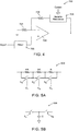
- FIG 4 shows a variable gain filter circuit 700 that can be used in the control circuit of Figures 1A to 3B in one embodiment of the invention.
- the variable gain filter circuit 700 includes an operational amplifier 720 with an inverting input, a non-inverting input, and an output.
- a filter circuit is connected to the non-inverting input.
- a first resistor 724, grounded, is connected with the inverting input.
- a second resistor 726 and a variable resistance circuit 728 are connected between the inverting input and the output of the operational amplifier 720.
- the variable resistance circuit provides a resistance that can be varied by a control signal, such as that from a controller, to change the gain factor K 1 .
- variable gain filter circuit 700 can be implemented using a circuit with a resistor network, a capacitor network, an inductor network, or any of their combination.
- FIG. 5A shows a variable resistance circuit 800 in the variable gain filter circuit of Figure 4 in one embodiment of the invention.
- the variable resistance circuit 800 includes three resistors R, 2R, 4R, each respective connected in parallel with a switch S 1 , S 2 , S 3 .
- Each of the switches S 1 , S 2 , S 3 is arranged to receive a respective control signal C 1 , C 2 , C 3 .
- the equivalent resistance of the variable resistance circuit 800 can be changed to affect the gain factor K 1 .
- the equivalent resistance of the circuit 800 can change from o to 7R with incremental steps of R.
- Figure 5B is a variable resistance circuit 900 in the variable gain filter circuit of Figure 4 in another embodiment of the invention.
- the circuit 900 includes a switched capacitor, a capacitor C operably connected at two ends with a respective switch S 4 , S 5 .
- Each of the switches S 4 , S 5 is arranged to receive a respective control signal.
- the equivalent resistance of the variable resistance circuit 900 can be changed to affect the gain factor K 1 .
- the equivalent resistance of the circuit 900 is a function of switching frequency.
- variable resistance circuits 800, 900 can be made.
- the number and resistance of the resistors in circuit 800 can be modified based on applications.
- the number and capacitance of the capacitor in circuit 900 can be modified based on applications.
- control circuits in all of the above embodiments can be readily embodied in an integrated circuit.
- the above embodiments of the invention provide a variable gain control circuit, the gain factor of which can be adjusted as needed to ensure that the overall gain of the circuit can be maintained at or substantially at 1, to improve interference suppression performance.
- This aspect is particularly advantageous because the overall gain or gain product can be affected by various factors, such as
Landscapes
- Engineering & Computer Science (AREA)
- Physics & Mathematics (AREA)
- Electromagnetism (AREA)
- Power Engineering (AREA)
- Computer Networks & Wireless Communication (AREA)
- Signal Processing (AREA)
- Networks Using Active Elements (AREA)
- Control Of Amplification And Gain Control (AREA)
Applications Claiming Priority (1)
| Application Number | Priority Date | Filing Date | Title |
|---|---|---|---|
| US16/185,275 US10396656B1 (en) | 2018-11-09 | 2018-11-09 | Control circuit for suppressing electromagnetic interference signals |
Publications (2)
| Publication Number | Publication Date |
|---|---|
| EP3651385A1 true EP3651385A1 (fr) | 2020-05-13 |
| EP3651385B1 EP3651385B1 (fr) | 2021-08-25 |
Family
ID=67700590
Family Applications (1)
| Application Number | Title | Priority Date | Filing Date |
|---|---|---|---|
| EP19208121.4A Active EP3651385B1 (fr) | 2018-11-09 | 2019-11-08 | Circuit de commande pour supprimer des signaux d'interférence électromagnétique |
Country Status (4)
| Country | Link |
|---|---|
| US (1) | US10396656B1 (fr) |
| EP (1) | EP3651385B1 (fr) |
| CN (1) | CN111181378A (fr) |
| TW (1) | TWI869358B (fr) |
Families Citing this family (7)
| Publication number | Priority date | Publication date | Assignee | Title |
|---|---|---|---|---|
| WO2021030964A1 (fr) * | 2019-08-16 | 2021-02-25 | AnApp Technologies Limited | Circuit de suppression d'interférence électromagnétique |
| WO2022016395A1 (fr) | 2020-07-21 | 2022-01-27 | AnApp Technologies Limited | Circuit de suppression d'interférence électromagnétique et circuit de détection associé |
| TWI790956B (zh) * | 2022-03-31 | 2023-01-21 | 宏碁股份有限公司 | 抑制噪音之電源供應器 |
| CN115996033A (zh) * | 2023-03-22 | 2023-04-21 | 敏业信息科技(上海)有限公司 | 一种电磁干扰滤波器 |
| CN116015048B (zh) * | 2023-03-27 | 2023-05-30 | 杭州顺元微电子有限公司 | 一种电磁辐射均衡器 |
| CN118873204B (zh) * | 2024-07-16 | 2025-05-13 | 上海三友医疗器械股份有限公司 | 髓内钉定位方法和系统 |
| CN121077432B (zh) * | 2025-11-10 | 2026-02-03 | 嘉兴翼波电子有限公司 | 一种远端高抑制管状低通滤波器及其控制方法 |
Citations (3)
| Publication number | Priority date | Publication date | Assignee | Title |
|---|---|---|---|---|
| US4730243A (en) * | 1985-12-23 | 1988-03-08 | Sundstrand Corporation | EMI reduction circuit |
| US5490030A (en) * | 1994-01-31 | 1996-02-06 | Taylor; Harold L. | Electromagnetic and radio frequency interference suppression for ground fault circuit interrupters |
| US8823448B1 (en) * | 2013-03-29 | 2014-09-02 | Hamilton Sundstrand Corporation | Feed forward active EMI filters |
Family Cites Families (9)
| Publication number | Priority date | Publication date | Assignee | Title |
|---|---|---|---|---|
| US6052420A (en) * | 1997-05-15 | 2000-04-18 | Northern Telecom Limited | Adaptive multiple sub-band common-mode RFI suppression |
| US6940973B1 (en) * | 1999-06-07 | 2005-09-06 | Bell Canada | Method and apparatus for cancelling common mode noise occurring in communications channels |
| US6775157B2 (en) * | 2002-06-25 | 2004-08-10 | International Rectifier Corporation | Closed loop active EMI filter for reducing common or differential noise based on an error value |
| CN101295924B (zh) * | 2008-05-22 | 2010-06-09 | 中国人民解放军海军工程大学 | 消除互感耦合电磁干扰的方法和装置 |
| TWI521843B (zh) * | 2014-12-16 | 2016-02-11 | 晶焱科技股份有限公司 | 消弭電源式電磁干擾之濾波器 |
| KR101710781B1 (ko) * | 2015-04-15 | 2017-02-27 | 강원대학교산학협력단 | Cm 필터와 dm 필터를 결합한 능동 emi 필터 장치 |
| CN205864262U (zh) * | 2016-06-08 | 2017-01-04 | 昂宝电子(上海)有限公司 | 电源转换电路 |
| CN108233355A (zh) * | 2018-05-25 | 2018-06-29 | 敏业信息科技(上海)有限公司 | 共模电磁噪声注入网络及有源电磁干扰滤波器 |
| CN108418569B (zh) * | 2018-05-25 | 2018-11-09 | 敏业信息科技(上海)有限公司 | 差模电磁噪声注入网络及有源电磁干扰滤波器 |
-
2018
- 2018-11-09 US US16/185,275 patent/US10396656B1/en active Active
-
2019
- 2019-11-08 TW TW108140698A patent/TWI869358B/zh active
- 2019-11-08 EP EP19208121.4A patent/EP3651385B1/fr active Active
- 2019-11-11 CN CN201911093434.XA patent/CN111181378A/zh active Pending
Patent Citations (3)
| Publication number | Priority date | Publication date | Assignee | Title |
|---|---|---|---|---|
| US4730243A (en) * | 1985-12-23 | 1988-03-08 | Sundstrand Corporation | EMI reduction circuit |
| US5490030A (en) * | 1994-01-31 | 1996-02-06 | Taylor; Harold L. | Electromagnetic and radio frequency interference suppression for ground fault circuit interrupters |
| US8823448B1 (en) * | 2013-03-29 | 2014-09-02 | Hamilton Sundstrand Corporation | Feed forward active EMI filters |
Also Published As
| Publication number | Publication date |
|---|---|
| TWI869358B (zh) | 2025-01-11 |
| TW202027392A (zh) | 2020-07-16 |
| CN111181378A (zh) | 2020-05-19 |
| EP3651385B1 (fr) | 2021-08-25 |
| US10396656B1 (en) | 2019-08-27 |
Similar Documents
| Publication | Publication Date | Title |
|---|---|---|
| EP3651385A1 (fr) | Circuit de commande pour supprimer des signaux d'interférence électromagnétique | |
| US7504814B2 (en) | Current generating apparatus and feedback-controlled system utilizing the current generating apparatus | |
| US20130082672A1 (en) | Capacitor-free low drop-out regulator | |
| US6552629B2 (en) | Universally stable output filter | |
| US10320280B2 (en) | LC filter including coupled inductors for reducing ripple in switching power supplies | |
| JP7321377B2 (ja) | ノイズフィルタ | |
| US11418031B2 (en) | Actively-controlled power transformer and method for controlling | |
| US20110133710A1 (en) | Partial Feedback Mechanism in Voltage Regulators to Reduce Output Noise Coupling and DC Voltage Shift at Output | |
| US20180212592A1 (en) | Second order switched capacitor filter | |
| US9666375B2 (en) | Voltage smoothing circuit, voltage conversion circuit, and method for controlling voltage to be applied to multilayer capacitor | |
| JP2021005459A (ja) | 誘電加熱システム | |
| US11754611B2 (en) | Electromagnetic interference suppression circuit and related sensing circuit | |
| US11545934B2 (en) | Oscillating signal generator circuit | |
| JP3012616B1 (ja) | 過電圧保護回路 | |
| US1921788A (en) | Electric control system | |
| JP7084479B2 (ja) | 定電圧発生回路 | |
| KR101970205B1 (ko) | 위상조정회로, 인버터회로 및 급전장치 | |
| US12597915B2 (en) | Capacitance circuit | |
| Amaya et al. | Improving Low-Dropout Regulator Frequency Stability by Exploiting the Equivalent Series Resistor and Featuring an Adaptive Biasing Strategy | |
| US2944207A (en) | Current loss compensating device | |
| JPH0586090B2 (fr) | ||
| JP2025043940A (ja) | 等価回路 | |
| WO2017001253A1 (fr) | Détecteur de proximité par induction à réglage électronique | |
| SU549796A1 (ru) | Импульсный стабилизатор посто нного напр жени | |
| AT521551A1 (de) | Vorrichtung zur Stabilisierung sowie zum Filtern von Störungen bei einem Mehrphasen-Wechselspannungsnetz |
Legal Events
| Date | Code | Title | Description |
|---|---|---|---|
| PUAI | Public reference made under article 153(3) epc to a published international application that has entered the european phase |
Free format text: ORIGINAL CODE: 0009012 |
|
| STAA | Information on the status of an ep patent application or granted ep patent |
Free format text: STATUS: THE APPLICATION HAS BEEN PUBLISHED |
|
| AK | Designated contracting states |
Kind code of ref document: A1 Designated state(s): AL AT BE BG CH CY CZ DE DK EE ES FI FR GB GR HR HU IE IS IT LI LT LU LV MC MK MT NL NO PL PT RO RS SE SI SK SM TR |
|
| AX | Request for extension of the european patent |
Extension state: BA ME |
|
| STAA | Information on the status of an ep patent application or granted ep patent |
Free format text: STATUS: REQUEST FOR EXAMINATION WAS MADE |
|
| STAA | Information on the status of an ep patent application or granted ep patent |
Free format text: STATUS: EXAMINATION IS IN PROGRESS |
|
| 17P | Request for examination filed |
Effective date: 20201113 |
|
| RBV | Designated contracting states (corrected) |
Designated state(s): AL AT BE BG CH CY CZ DE DK EE ES FI FR GB GR HR HU IE IS IT LI LT LU LV MC MK MT NL NO PL PT RO RS SE SI SK SM TR |
|
| 17Q | First examination report despatched |
Effective date: 20201209 |
|
| GRAP | Despatch of communication of intention to grant a patent |
Free format text: ORIGINAL CODE: EPIDOSNIGR1 |
|
| STAA | Information on the status of an ep patent application or granted ep patent |
Free format text: STATUS: GRANT OF PATENT IS INTENDED |
|
| INTG | Intention to grant announced |
Effective date: 20210316 |
|
| GRAS | Grant fee paid |
Free format text: ORIGINAL CODE: EPIDOSNIGR3 |
|
| GRAA | (expected) grant |
Free format text: ORIGINAL CODE: 0009210 |
|
| STAA | Information on the status of an ep patent application or granted ep patent |
Free format text: STATUS: THE PATENT HAS BEEN GRANTED |
|
| AK | Designated contracting states |
Kind code of ref document: B1 Designated state(s): AL AT BE BG CH CY CZ DE DK EE ES FI FR GB GR HR HU IE IS IT LI LT LU LV MC MK MT NL NO PL PT RO RS SE SI SK SM TR |
|
| REG | Reference to a national code |
Ref country code: CH Ref legal event code: EP |
|
| REG | Reference to a national code |
Ref country code: IE Ref legal event code: FG4D Ref country code: AT Ref legal event code: REF Ref document number: 1424879 Country of ref document: AT Kind code of ref document: T Effective date: 20210915 |
|
| REG | Reference to a national code |
Ref country code: DE Ref legal event code: R096 Ref document number: 602019007152 Country of ref document: DE |
|
| REG | Reference to a national code |
Ref country code: LT Ref legal event code: MG9D |
|
| REG | Reference to a national code |
Ref country code: NL Ref legal event code: MP Effective date: 20210825 |
|
| REG | Reference to a national code |
Ref country code: AT Ref legal event code: MK05 Ref document number: 1424879 Country of ref document: AT Kind code of ref document: T Effective date: 20210825 |
|
| PG25 | Lapsed in a contracting state [announced via postgrant information from national office to epo] |
Ref country code: SE Free format text: LAPSE BECAUSE OF FAILURE TO SUBMIT A TRANSLATION OF THE DESCRIPTION OR TO PAY THE FEE WITHIN THE PRESCRIBED TIME-LIMIT Effective date: 20210825 Ref country code: RS Free format text: LAPSE BECAUSE OF FAILURE TO SUBMIT A TRANSLATION OF THE DESCRIPTION OR TO PAY THE FEE WITHIN THE PRESCRIBED TIME-LIMIT Effective date: 20210825 Ref country code: ES Free format text: LAPSE BECAUSE OF FAILURE TO SUBMIT A TRANSLATION OF THE DESCRIPTION OR TO PAY THE FEE WITHIN THE PRESCRIBED TIME-LIMIT Effective date: 20210825 Ref country code: LT Free format text: LAPSE BECAUSE OF FAILURE TO SUBMIT A TRANSLATION OF THE DESCRIPTION OR TO PAY THE FEE WITHIN THE PRESCRIBED TIME-LIMIT Effective date: 20210825 Ref country code: BG Free format text: LAPSE BECAUSE OF FAILURE TO SUBMIT A TRANSLATION OF THE DESCRIPTION OR TO PAY THE FEE WITHIN THE PRESCRIBED TIME-LIMIT Effective date: 20211125 Ref country code: AT Free format text: LAPSE BECAUSE OF FAILURE TO SUBMIT A TRANSLATION OF THE DESCRIPTION OR TO PAY THE FEE WITHIN THE PRESCRIBED TIME-LIMIT Effective date: 20210825 Ref country code: FI Free format text: LAPSE BECAUSE OF FAILURE TO SUBMIT A TRANSLATION OF THE DESCRIPTION OR TO PAY THE FEE WITHIN THE PRESCRIBED TIME-LIMIT Effective date: 20210825 Ref country code: HR Free format text: LAPSE BECAUSE OF FAILURE TO SUBMIT A TRANSLATION OF THE DESCRIPTION OR TO PAY THE FEE WITHIN THE PRESCRIBED TIME-LIMIT Effective date: 20210825 Ref country code: PT Free format text: LAPSE BECAUSE OF FAILURE TO SUBMIT A TRANSLATION OF THE DESCRIPTION OR TO PAY THE FEE WITHIN THE PRESCRIBED TIME-LIMIT Effective date: 20211227 Ref country code: NO Free format text: LAPSE BECAUSE OF FAILURE TO SUBMIT A TRANSLATION OF THE DESCRIPTION OR TO PAY THE FEE WITHIN THE PRESCRIBED TIME-LIMIT Effective date: 20211125 |
|
| PG25 | Lapsed in a contracting state [announced via postgrant information from national office to epo] |
Ref country code: PL Free format text: LAPSE BECAUSE OF FAILURE TO SUBMIT A TRANSLATION OF THE DESCRIPTION OR TO PAY THE FEE WITHIN THE PRESCRIBED TIME-LIMIT Effective date: 20210825 Ref country code: LV Free format text: LAPSE BECAUSE OF FAILURE TO SUBMIT A TRANSLATION OF THE DESCRIPTION OR TO PAY THE FEE WITHIN THE PRESCRIBED TIME-LIMIT Effective date: 20210825 Ref country code: GR Free format text: LAPSE BECAUSE OF FAILURE TO SUBMIT A TRANSLATION OF THE DESCRIPTION OR TO PAY THE FEE WITHIN THE PRESCRIBED TIME-LIMIT Effective date: 20211126 |
|
| PG25 | Lapsed in a contracting state [announced via postgrant information from national office to epo] |
Ref country code: NL Free format text: LAPSE BECAUSE OF FAILURE TO SUBMIT A TRANSLATION OF THE DESCRIPTION OR TO PAY THE FEE WITHIN THE PRESCRIBED TIME-LIMIT Effective date: 20210825 |
|
| PG25 | Lapsed in a contracting state [announced via postgrant information from national office to epo] |
Ref country code: DK Free format text: LAPSE BECAUSE OF FAILURE TO SUBMIT A TRANSLATION OF THE DESCRIPTION OR TO PAY THE FEE WITHIN THE PRESCRIBED TIME-LIMIT Effective date: 20210825 |
|
| REG | Reference to a national code |
Ref country code: DE Ref legal event code: R097 Ref document number: 602019007152 Country of ref document: DE |
|
| PG25 | Lapsed in a contracting state [announced via postgrant information from national office to epo] |
Ref country code: SM Free format text: LAPSE BECAUSE OF FAILURE TO SUBMIT A TRANSLATION OF THE DESCRIPTION OR TO PAY THE FEE WITHIN THE PRESCRIBED TIME-LIMIT Effective date: 20210825 Ref country code: SK Free format text: LAPSE BECAUSE OF FAILURE TO SUBMIT A TRANSLATION OF THE DESCRIPTION OR TO PAY THE FEE WITHIN THE PRESCRIBED TIME-LIMIT Effective date: 20210825 Ref country code: RO Free format text: LAPSE BECAUSE OF FAILURE TO SUBMIT A TRANSLATION OF THE DESCRIPTION OR TO PAY THE FEE WITHIN THE PRESCRIBED TIME-LIMIT Effective date: 20210825 Ref country code: EE Free format text: LAPSE BECAUSE OF FAILURE TO SUBMIT A TRANSLATION OF THE DESCRIPTION OR TO PAY THE FEE WITHIN THE PRESCRIBED TIME-LIMIT Effective date: 20210825 Ref country code: CZ Free format text: LAPSE BECAUSE OF FAILURE TO SUBMIT A TRANSLATION OF THE DESCRIPTION OR TO PAY THE FEE WITHIN THE PRESCRIBED TIME-LIMIT Effective date: 20210825 Ref country code: AL Free format text: LAPSE BECAUSE OF FAILURE TO SUBMIT A TRANSLATION OF THE DESCRIPTION OR TO PAY THE FEE WITHIN THE PRESCRIBED TIME-LIMIT Effective date: 20210825 |
|
| PG25 | Lapsed in a contracting state [announced via postgrant information from national office to epo] |
Ref country code: MC Free format text: LAPSE BECAUSE OF FAILURE TO SUBMIT A TRANSLATION OF THE DESCRIPTION OR TO PAY THE FEE WITHIN THE PRESCRIBED TIME-LIMIT Effective date: 20210825 |
|
| PLBE | No opposition filed within time limit |
Free format text: ORIGINAL CODE: 0009261 |
|
| STAA | Information on the status of an ep patent application or granted ep patent |
Free format text: STATUS: NO OPPOSITION FILED WITHIN TIME LIMIT |
|
| PG25 | Lapsed in a contracting state [announced via postgrant information from national office to epo] |
Ref country code: LU Free format text: LAPSE BECAUSE OF NON-PAYMENT OF DUE FEES Effective date: 20211108 Ref country code: IT Free format text: LAPSE BECAUSE OF FAILURE TO SUBMIT A TRANSLATION OF THE DESCRIPTION OR TO PAY THE FEE WITHIN THE PRESCRIBED TIME-LIMIT Effective date: 20210825 Ref country code: BE Free format text: LAPSE BECAUSE OF NON-PAYMENT OF DUE FEES Effective date: 20211130 |
|
| REG | Reference to a national code |
Ref country code: BE Ref legal event code: MM Effective date: 20211130 |
|
| 26N | No opposition filed |
Effective date: 20220527 |
|
| PG25 | Lapsed in a contracting state [announced via postgrant information from national office to epo] |
Ref country code: SI Free format text: LAPSE BECAUSE OF FAILURE TO SUBMIT A TRANSLATION OF THE DESCRIPTION OR TO PAY THE FEE WITHIN THE PRESCRIBED TIME-LIMIT Effective date: 20210825 |
|
| PG25 | Lapsed in a contracting state [announced via postgrant information from national office to epo] |
Ref country code: IE Free format text: LAPSE BECAUSE OF NON-PAYMENT OF DUE FEES Effective date: 20211108 |
|
| PG25 | Lapsed in a contracting state [announced via postgrant information from national office to epo] |
Ref country code: CY Free format text: LAPSE BECAUSE OF FAILURE TO SUBMIT A TRANSLATION OF THE DESCRIPTION OR TO PAY THE FEE WITHIN THE PRESCRIBED TIME-LIMIT Effective date: 20210825 |
|
| REG | Reference to a national code |
Ref country code: CH Ref legal event code: PL |
|
| PG25 | Lapsed in a contracting state [announced via postgrant information from national office to epo] |
Ref country code: LI Free format text: LAPSE BECAUSE OF NON-PAYMENT OF DUE FEES Effective date: 20221130 Ref country code: HU Free format text: LAPSE BECAUSE OF FAILURE TO SUBMIT A TRANSLATION OF THE DESCRIPTION OR TO PAY THE FEE WITHIN THE PRESCRIBED TIME-LIMIT; INVALID AB INITIO Effective date: 20191108 Ref country code: CH Free format text: LAPSE BECAUSE OF NON-PAYMENT OF DUE FEES Effective date: 20221130 |
|
| PG25 | Lapsed in a contracting state [announced via postgrant information from national office to epo] |
Ref country code: MK Free format text: LAPSE BECAUSE OF FAILURE TO SUBMIT A TRANSLATION OF THE DESCRIPTION OR TO PAY THE FEE WITHIN THE PRESCRIBED TIME-LIMIT Effective date: 20210825 |
|
| REG | Reference to a national code |
Ref country code: GB Ref legal event code: 732E Free format text: REGISTERED BETWEEN 20240411 AND 20240417 |
|
| REG | Reference to a national code |
Ref country code: DE Ref legal event code: R081 Ref document number: 602019007152 Country of ref document: DE Owner name: POWER GREEN TECHNOLOGIES INC., OAKLAND, US Free format text: FORMER OWNER: ANAPP TECHNOLOGIES LTD, KOWLOON, HK |
|
| PG25 | Lapsed in a contracting state [announced via postgrant information from national office to epo] |
Ref country code: MT Free format text: LAPSE BECAUSE OF FAILURE TO SUBMIT A TRANSLATION OF THE DESCRIPTION OR TO PAY THE FEE WITHIN THE PRESCRIBED TIME-LIMIT Effective date: 20210825 |
|
| PGFP | Annual fee paid to national office [announced via postgrant information from national office to epo] |
Ref country code: GB Payment date: 20250926 Year of fee payment: 7 |
|
| PG25 | Lapsed in a contracting state [announced via postgrant information from national office to epo] |
Ref country code: TR Free format text: LAPSE BECAUSE OF FAILURE TO SUBMIT A TRANSLATION OF THE DESCRIPTION OR TO PAY THE FEE WITHIN THE PRESCRIBED TIME-LIMIT Effective date: 20210825 |
|
| PGFP | Annual fee paid to national office [announced via postgrant information from national office to epo] |
Ref country code: DE Payment date: 20251118 Year of fee payment: 7 |
|
| PGFP | Annual fee paid to national office [announced via postgrant information from national office to epo] |
Ref country code: FR Payment date: 20251114 Year of fee payment: 7 |