EP1652009B1 - Verfahren zur herstellung von mustern mit geneigten flanken mittels fotolithographie - Google Patents
Verfahren zur herstellung von mustern mit geneigten flanken mittels fotolithographie Download PDFInfo
- Publication number
- EP1652009B1 EP1652009B1 EP04786375A EP04786375A EP1652009B1 EP 1652009 B1 EP1652009 B1 EP 1652009B1 EP 04786375 A EP04786375 A EP 04786375A EP 04786375 A EP04786375 A EP 04786375A EP 1652009 B1 EP1652009 B1 EP 1652009B1
- Authority
- EP
- European Patent Office
- Prior art keywords
- mask
- layer
- substrate
- optical system
- photosensitive resin
- Prior art date
- Legal status (The legal status is an assumption and is not a legal conclusion. Google has not performed a legal analysis and makes no representation as to the accuracy of the status listed.)
- Expired - Lifetime
Links
- 238000004519 manufacturing process Methods 0.000 title claims abstract description 16
- 238000000206 photolithography Methods 0.000 title claims description 31
- 239000011347 resin Substances 0.000 claims abstract description 134
- 229920005989 resin Polymers 0.000 claims abstract description 134
- 239000000758 substrate Substances 0.000 claims abstract description 103
- 238000000034 method Methods 0.000 claims abstract description 75
- 230000003287 optical effect Effects 0.000 claims description 103
- 230000006978 adaptation Effects 0.000 claims description 19
- 238000000151 deposition Methods 0.000 claims description 15
- 239000000463 material Substances 0.000 claims description 14
- 239000007788 liquid Substances 0.000 claims description 9
- XLYOFNOQVPJJNP-UHFFFAOYSA-N water Substances O XLYOFNOQVPJJNP-UHFFFAOYSA-N 0.000 claims description 7
- 239000012530 fluid Substances 0.000 claims description 6
- 230000000284 resting effect Effects 0.000 claims description 3
- 239000010410 layer Substances 0.000 description 231
- 229920002120 photoresistant polymer Polymers 0.000 description 70
- 230000008569 process Effects 0.000 description 22
- VYPSYNLAJGMNEJ-UHFFFAOYSA-N Silicium dioxide Chemical compound O=[Si]=O VYPSYNLAJGMNEJ-UHFFFAOYSA-N 0.000 description 18
- PEDCQBHIVMGVHV-UHFFFAOYSA-N Glycerine Chemical compound OCC(O)CO PEDCQBHIVMGVHV-UHFFFAOYSA-N 0.000 description 16
- 230000003071 parasitic effect Effects 0.000 description 13
- 230000002745 absorbent Effects 0.000 description 12
- 239000002250 absorbent Substances 0.000 description 12
- 229920000642 polymer Polymers 0.000 description 9
- 229920000297 Rayon Polymers 0.000 description 8
- 239000002964 rayon Substances 0.000 description 8
- 239000000377 silicon dioxide Substances 0.000 description 8
- 235000011187 glycerol Nutrition 0.000 description 7
- 229920001486 SU-8 photoresist Polymers 0.000 description 5
- 229910052751 metal Inorganic materials 0.000 description 5
- 239000002184 metal Substances 0.000 description 5
- 239000011521 glass Substances 0.000 description 4
- VYZAMTAEIAYCRO-UHFFFAOYSA-N Chromium Chemical compound [Cr] VYZAMTAEIAYCRO-UHFFFAOYSA-N 0.000 description 3
- XUIMIQQOPSSXEZ-UHFFFAOYSA-N Silicon Chemical compound [Si] XUIMIQQOPSSXEZ-UHFFFAOYSA-N 0.000 description 3
- 229910052804 chromium Inorganic materials 0.000 description 3
- 239000011651 chromium Substances 0.000 description 3
- 238000007796 conventional method Methods 0.000 description 3
- 238000001459 lithography Methods 0.000 description 3
- 229910052710 silicon Inorganic materials 0.000 description 3
- 239000010703 silicon Substances 0.000 description 3
- OKTJSMMVPCPJKN-UHFFFAOYSA-N Carbon Chemical compound [C] OKTJSMMVPCPJKN-UHFFFAOYSA-N 0.000 description 2
- 238000001015 X-ray lithography Methods 0.000 description 2
- 238000012550 audit Methods 0.000 description 2
- 230000008901 benefit Effects 0.000 description 2
- 239000011247 coating layer Substances 0.000 description 2
- 230000008021 deposition Effects 0.000 description 2
- 230000000670 limiting effect Effects 0.000 description 2
- 230000000149 penetrating effect Effects 0.000 description 2
- 229920003229 poly(methyl methacrylate) Polymers 0.000 description 2
- 239000004926 polymethyl methacrylate Substances 0.000 description 2
- 239000004576 sand Substances 0.000 description 2
- 239000000126 substance Substances 0.000 description 2
- CERQOIWHTDAKMF-UHFFFAOYSA-M Methacrylate Chemical compound CC(=C)C([O-])=O CERQOIWHTDAKMF-UHFFFAOYSA-M 0.000 description 1
- 241001465805 Nymphalidae Species 0.000 description 1
- 239000004642 Polyimide Substances 0.000 description 1
- 229910004298 SiO 2 Inorganic materials 0.000 description 1
- 229910010413 TiO 2 Inorganic materials 0.000 description 1
- RTAQQCXQSZGOHL-UHFFFAOYSA-N Titanium Chemical compound [Ti] RTAQQCXQSZGOHL-UHFFFAOYSA-N 0.000 description 1
- 229910052782 aluminium Inorganic materials 0.000 description 1
- XAGFODPZIPBFFR-UHFFFAOYSA-N aluminium Chemical compound [Al] XAGFODPZIPBFFR-UHFFFAOYSA-N 0.000 description 1
- 239000006117 anti-reflective coating Substances 0.000 description 1
- 230000003667 anti-reflective effect Effects 0.000 description 1
- 230000015572 biosynthetic process Effects 0.000 description 1
- 229910052799 carbon Inorganic materials 0.000 description 1
- 230000008878 coupling Effects 0.000 description 1
- 238000010168 coupling process Methods 0.000 description 1
- 238000005859 coupling reaction Methods 0.000 description 1
- 230000003247 decreasing effect Effects 0.000 description 1
- 229920001971 elastomer Polymers 0.000 description 1
- 239000000806 elastomer Substances 0.000 description 1
- 238000009713 electroplating Methods 0.000 description 1
- 229910052500 inorganic mineral Inorganic materials 0.000 description 1
- 230000001678 irradiating effect Effects 0.000 description 1
- 230000001788 irregular Effects 0.000 description 1
- 239000011707 mineral Substances 0.000 description 1
- 230000035515 penetration Effects 0.000 description 1
- 230000000704 physical effect Effects 0.000 description 1
- 239000000049 pigment Substances 0.000 description 1
- 229920001721 polyimide Polymers 0.000 description 1
- 239000011241 protective layer Substances 0.000 description 1
- 230000009467 reduction Effects 0.000 description 1
- 230000002829 reductive effect Effects 0.000 description 1
- 238000007493 shaping process Methods 0.000 description 1
- 239000002356 single layer Substances 0.000 description 1
- 239000002904 solvent Substances 0.000 description 1
- 239000010936 titanium Substances 0.000 description 1
- 229910052719 titanium Inorganic materials 0.000 description 1
Images



Classifications
-
- B—PERFORMING OPERATIONS; TRANSPORTING
- B81—MICROSTRUCTURAL TECHNOLOGY
- B81C—PROCESSES OR APPARATUS SPECIALLY ADAPTED FOR THE MANUFACTURE OR TREATMENT OF MICROSTRUCTURAL DEVICES OR SYSTEMS
- B81C1/00—Manufacture or treatment of devices or systems in or on a substrate
- B81C1/00015—Manufacture or treatment of devices or systems in or on a substrate for manufacturing microsystems
- B81C1/00023—Manufacture or treatment of devices or systems in or on a substrate for manufacturing microsystems without movable or flexible elements
- B81C1/00103—Structures having a predefined profile, e.g. sloped or rounded grooves
-
- G—PHYSICS
- G03—PHOTOGRAPHY; CINEMATOGRAPHY; ANALOGOUS TECHNIQUES USING WAVES OTHER THAN OPTICAL WAVES; ELECTROGRAPHY; HOLOGRAPHY
- G03F—PHOTOMECHANICAL PRODUCTION OF TEXTURED OR PATTERNED SURFACES, e.g. FOR PRINTING, FOR PROCESSING OF SEMICONDUCTOR DEVICES; MATERIALS THEREFOR; ORIGINALS THEREFOR; APPARATUS SPECIALLY ADAPTED THEREFOR
- G03F7/00—Photomechanical, e.g. photolithographic, production of textured or patterned surfaces, e.g. printing surfaces; Materials therefor, e.g. comprising photoresists; Apparatus specially adapted therefor
- G03F7/70—Microphotolithographic exposure; Apparatus therefor
- G03F7/70216—Mask projection systems
-
- B—PERFORMING OPERATIONS; TRANSPORTING
- B81—MICROSTRUCTURAL TECHNOLOGY
- B81C—PROCESSES OR APPARATUS SPECIALLY ADAPTED FOR THE MANUFACTURE OR TREATMENT OF MICROSTRUCTURAL DEVICES OR SYSTEMS
- B81C2201/00—Manufacture or treatment of microstructural devices or systems
- B81C2201/01—Manufacture or treatment of microstructural devices or systems in or on a substrate
- B81C2201/0101—Shaping material; Structuring the bulk substrate or layers on the substrate; Film patterning
- B81C2201/0156—Lithographic techniques
- B81C2201/0159—Lithographic techniques not provided for in B81C2201/0157
Definitions
- the present invention relates to a controlled incidence photolithography process for the manufacture of micro-components or micro-systems and a device for carrying out the method.
- Photolithography is used in the manufacture of integrated circuits, it is also the basic technique for the manufacture of micro-structures such as MEMS (abbreviation Anglo-Saxon “Micro Electro Mechanical Systems” or micro-electro-mechanical systems). It consists in manufacturing predefined patterns on a suitable substrate (for example a silicon wafer) in order to locally modify the properties of this substrate (which makes it possible, for example, to make transistors) or to deposit metal at certain locations on the substrate for realize for example micro-machines.
- MEMS abbreviation Anglo-Saxon "Micro Electro Mechanical Systems” or micro-electro-mechanical systems
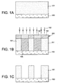
- a photolithography process is carried out at normal incidence (that is to say that a layer of resin to photo-structuring is usually perpendicular to the main direction of a beam of light rays through which it is insulated).
- a layer of photosensitive resin 101 for example hundred micrometers of polyimide
- a substrate 100 for example silicon
- This layer of photosensitive resin 101 is then exposed so as to make patterns therein, using a beam of light rays 102 (generally of wavelength located in the ultraviolet range) orthogonal to the main plane of light.
- the resin layer 101 through a mask 103 having opaque portions 104 (for example metal) to the beam of light ray 102 and transparent portions 105 (for example silica) to the beam of light rays 102, the transparent portions 105 being able to to be holes.
- the transparent portions 105 are arranged according to the patterns that one wishes to achieve.
- the image of the mask 103 is then projected on the photosensitive resin layer 101. Some parts of the resin layer 101 are at this time exposed to ultraviolet rays while others remain intact.
- the resin layer 101 thus comprises insolated zones 106 and non-insolated zones 107 corresponding to the portions of the resin layer 101 protected by the mask 103 (FIG. 1B).
- the mask 103 is removed, then the resin layer 101 is developed with chemicals such as, for example, a strong base, which remove the insolated zones 106 from the resin layer 101 and leave the non-insolated zones 107 in the where the resin of the resin layer 101 is a "positive" type resin ( Figure 1C).
- chemicals such as, for example, a strong base, which remove the insolated zones 106 from the resin layer 101 and leave the non-insolated zones 107 in the where the resin of the resin layer 101 is a "positive" type resin ( Figure 1C).
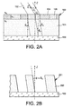
- FIG. 1A An example of a method for producing sloping flank resin patterns is first of all to deposit a layer of photosensitive resin 101 on a substrate 100 as illustrated in FIG. 1A.
- the photoresist layer 101 has a refractive index N 2 .
- a mask 103 is attached to this resin layer 101.
- the mask 103 has opaque portions 104, for example made of chromium, and transparent portions 105, for example made of silica having a refractive index N 1 .
- the substrate 100 covered with the photoresist layer 101 and the mask 103 form an assembly that is tilted under a beam of ultraviolet light beams 102 of main direction d ⁇ 1 .
- the beam of light rays 102 passes through an air layer of refractive index N 0 approximately equal to 1 and achieves an angle of incidence Î 1 on the mask 103 with respect to a normal not ⁇ at the main plane of the substrate 100 before penetrating through the transparent portions 105 of the mask 103.
- the light beam 102 is then refracted as it passes through the transparent portions 105 of the mask 103.
- the main direction d ⁇ 1 beam 102 is then deflected and makes an incident angle R 1 on the resin layer 101 with a normal not ⁇ at the main plane of the substrate 100 as the beam is about to pass through the photosensitive resin layer 101.
- the incident angle R 1 on the resin layer 101 is less than the angle of incidence Î 1 on the mask 103 since the beam passes air to a more refractive medium (N 1 > N 0 ).
- the light beam 102 then penetrates through the photoresist layer 101 of refractive index N 2 .
- the beam of light rays 102 is then refracted again.
- the main direction d ⁇ 1 beam 102 achieves with normal not ⁇ , an angle resulting from exposure R 2 as a function of the incident angle R 1 , N 2 and N 1 (FIG. 2A).
- the layer of photosensitive resin 101 is thus insolated by a beam of light rays 102 inclined and achieving an angle resulting from insolation R 2 with the normal not ⁇ the main plane of the substrate 100.
- the mask 103 is removed from the photosensitive resin layer 101.
- the photosensitive resin layer 101 is developed, for example using a strong base.
- resin patterns 200 with inclined sides 201 are obtained (FIG. 2B).
- the inclined flanks 201 of the patterns 200 form an angle ⁇ with a normal not ⁇ at the main plane of the substrate 100, approximately equal to the resulting angle of insolation R 2 .
- the angle ⁇ of the flanks 201 of the patterns 200 is strongly limited. Indeed, during the insolation step, the beam of light rays 102 first inevitably passes through an air layer of index N 0 , then a mask of index N 1 approximately equal to 1.45 by example for a silica mask, then a layer of photoresist 101 of refractive index approximately equal to 1.6 (1.67 for a resin layer 101 SU-8 type). The large difference in refractive index between the air layer and the mask 103 and the difference in refractive index between the mask 103 and the photosensitive resin layer 101, cause a significant difference between the angle of incidence.
- the angle ⁇ of the sidewalls 201 of patterns 200 (approximately equal to R 2 ) that the inclined sides 201 of the resin patterns 200 produce with the normal not ⁇ so is also limited.
- the limitation of the angle ⁇ of the resin patterns 200 is very disadvantageous. It prevents the ability to manufacture many micro-structures. The realization for example micro-prisms at angles of 45 ° is impossible with such a method.
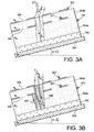
- an angle ⁇ is first inclined, a substrate 100 covered with a layer of photosensitive resin 101, under a beam of ultraviolet light rays 102. main direction d ⁇ 1 with the aid of a tilting plate 300 on which the substrate 100 rests.
- the layer of photosensitive resin 101 is insolated through two masks 301, 302 integrated directly into the layer of photosensitive resin 101.
- the layer of photosensitive resin is composed of a base sub-layer 303a of refractive index N 2 which rests on the substrate 100 and an intermediate sub-layer 303b situated above the base sub-layer 303a and with a refractive index N 1 equal to N 2 .
- the masks 301, 302 are each composed of a metal layer of titanium or aluminum separated from each other by the intermediate photosensitive resin sublayer 303b.
- the mask 301 comprises openings 304.
- the mask 302 comprises openings 305 which are identical but offset laterally slightly with respect to the openings 304.
- the main direction d ⁇ 1 beam 102 achieves an angle of incidence Î 1 on the mask 301 with a normal not ⁇ in the main plan of the substrate 100 equal to the angle of inclination ⁇ , before penetrating through the photosensitive resin layer 101.
- the beam 102 passes through the photosensitive resin layer 101, it is refracted and its main direction d ⁇ 1 achieves an angle resulting from insolation R 2 with normal not ⁇ the main plane of the substrate 100.
- the layer of photoresist 101 is thus exposed at an angle resulting from insolation R 2 .
- the masks 301, 302 being integrated with the photoresist layer 101, parasitic reflections, for example Fresnel-type reflections, are suppressed since there is no longer an air layer between mask and resin.
- the method of making inclined-walled patterns illustrated in FIG. 3A still has several disadvantages.
- the embodiment of the masks 302, 303 implies that this method is only valid for making simple patterns of relatively large size (of the order of ten micrometers), on the other hand it requires additional steps of photolithography to achieve the masks 302,303 integrated in the resin layer 101 relative to that shown in Figure 2A.
- the technique of making photolithographically inclined flanking patterns 3A always has the disadvantage that the inclination angle ⁇ of the inclined sides of the resin patterns remains limited.
- the document [2] referenced at the end of the present description proposes a method for reducing the reflection problems on the substrate 100.
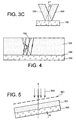
- the substrate 100 is subjected to a jet of 300 to 500 kPa pressure sand with SiC grains. This sand jet serves to render the surface 400 of the substrate 100 rough.
- This sand jet serves to render the surface 400 of the substrate 100 rough.
- the reflections of the beam of light beam 102 on the substrate 100 become irregular, which leads to a reduction of parasitic insolation areas (FIG. 4).
- this method has the disadvantage that it does not completely eliminate parasitic reflections, since it reduces the exposure time of the resin layer. index matching layer between the mask and the resin layer.
- US 2001/008741 discloses insolation through substrate using an optical system that allows the use of a standard apparatus for inclined insolation for the manufacture of microcomponents.
- the LIGA technique (LIGA for "Lithography Galvaniesirung und Abformung" is finished lithography by galvanization) consists in exposing a photoresist layer, for example a PMMA polymer (PMMA for polylmethyl methacrylate) using X-rays from a synchrotron. The layer of photoresist is then developed. Resin patterns of good definition are thus formed.
- a method derived from the LIGA method and described in documents [4] and [5] referenced at the end may be used. of the present description.
- This method described in FIG. 5 consists in making several exposures of a substrate 100 covered with a layer of photosensitive resin 101 and a mask 501 while keeping the mask 501-subtrat 100 assembly inclined with respect to a ray beam X 500 incident from a synchrotron (no in the areas of parasitic insolation by orienting the reflected light rays in very different directions.
- the document [3] referenced at the end of the present description proposes another method using a method that makes it possible in particular to reduce the problems of reflection on the substrate.
- the method includes coupling a plurality of polarizing filters to a light source to irradiate a substrate-based layer of photoresist with a beam of light rays, the beam being inclined relative to the substrate.
- the use of a circular polarizer filter coupled to a rectilinear polarizing filter makes it possible to significantly reduce the reflection problems on the substrate.
- Document [3] also discloses a method (not shown) for making curved resin patterns through the use of a "shadow mask” (or “shadow mask”).
- the "shadow mask” is a mask comprising opaque portions and transparent portions.
- the transparent parts of the "shadow mask” have the particularity of being covered with curved mounds made of polymer. It is these mounds, placed on the transparent parts of the mask that make it possible to obtain curved resin patterns.
- Document [3] also discloses the use of a layer of glycerol between the shadow mask and the resin-coated substrate to replace the layer of air inevitably between the shadow mask and the resin layer. The glycerol layer therefore serves represent).
- X-ray photolithography Unlike ultraviolet rays, the X-rays are hardly refracted when they penetrate through the photoresist layer 501. X-rays thus make it possible to obtain resin patterns having an angle of inclination with respect to a normal to a main plane of the substrate greater than that obtained by conventional techniques using ultraviolet rays. But X-ray photolithography nevertheless has significant disadvantages.
- a first disadvantage associated with the use of this technique is that the X-ray sources (synchrotrons) used to implement X-ray photolithography are very expensive and very cumbersome. Masks used in X-ray photolithography are also very expensive.
- X-ray photolithography because of its cost and difficulty of implementation is currently not used at the industrial level in integrated circuit manufacturing processes.
- the object of the present invention is to propose a process for producing patterns by photolithography as well as a device for carrying out this method.
- the method as well as the device are simple to implement and of reduced cost, unlike X-ray photolithography techniques.
- the present invention makes it possible to produce photolithographic patterns having inclined flanks at an angle much greater than those which the can be obtained with the prior art.
- the present invention also relates to a device as well as a method which make it possible to overcome the problems of parasitic reflections that occur, with some conventional methods of photolithography inclined light beam.
- the step of depositing the photoresist layer may be preceded by a step depositing at least one absorbent layer of light rays.
- an index matching layer may be deposited on the photoresist layer.
- an index matching layer in the form of a liquid or a gel chosen as a function of the index jump between the mask and the coating layer.
- the index matching layer has a refractive index greater than that of air and preferably between the refractive index of the mask and the refractive index of the photoresist layer.
- an index matching layer is placed between the optical system and the mask.
- This second index matching layer is for example in the form of a gel or a liquid deposited on the mask and which diffuses by capillarity between the optical system and the attached mask.
- This adaptation layer thus makes it possible to eliminate the Fresnel reflections between the optical system and the mask, and in step d) to obtain angles of inclination of the flanks of the resin patterns greater than those obtained in the art. prior.
- the optical system may comprise a prism, a diffraction grating, a network of micro-prisms or an optical diffuser.
- a prism, a diffraction grating, a micro-prism array or an optical diffuser are suitable optical systems, during the insolation phase to deflect the main direction of the beam of light rays by a predetermined deflection angle so that it has an angle of incidence on the non-zero mask with a normal to the main plane of the substrate as it penetrates through the mask.
- the angle of incidence on the mask can vary.
- the angle of incidence on the mask that the main direction of the light beam can be varied with can be varied. normal to the main plane of the substrate.
- the resulting angle of insolation of the photosensitive resin layer can be varied and in this way, after development, resin patterns with sidewalls having a variable inclination angle can be obtained.
- the optical system and on the other hand the substrate can be moved relative to one another, the mask being associated with either the optical system or the substrate.
- the optical system for example a prism
- the optical system can remain fixed while an assembly formed by the substrate, the photoresist layer and the mask turns on itself.
- the optical system for example a diffraction grating
- the mask associated with the optical system can also turn on itself while the substrate coated with the photoresist layer remains fixed.
- a set formed by the optical system, the mask, and the substrate can be moved relative to the beam of light rays.
- an assembly formed by the optical system, for example a prism, by the substrate, the photosensitive resin layer can be fixed while the main direction of the light beam beam varies. This can make it possible to obtain patterns of variable inclination resin.
- the invention also relates to a device for producing one or more patterns inclined by photolithography, comprising a plate on which a substrate rests, on which a layer of photosensitive resin, a mask, means for insolating the layer of photoresist to by means of a beam of light rays having a main direction, the beam of light rays passing through an optical system deviating from a predetermined deflection angle the main direction of the light beam so that the main direction of the beam is angle of incidence on the non-zero mask with a normal to the main plane of the substrate at the moment when the beam of light rays penetrates through the mask.
- the invention further relates to a device for producing one or more photolithographically inclined patterns comprising a substrate on which a layer of photoresist resides, the device further comprising a refractive index mask attached to said photosensitive resin layer or an index matching layer resting on said resin layer, an optical system attached to the mask or at an index matching layer based on the mask, means for irradiating the photosensitive resin layer with a beam of light rays having a certain main direction, the optical system being able to deviate from a predetermined deflection angle the main direction of the beam, so that the main direction of the light beam has an angle of incidence on the non-zero mask with a normal to the main plane of the substrate at the moment the beam of light rays penetrates to through the mask.
- the mask of the device comprises one or more openings.
- the optical system and the openings of the mask may have close refractive indices.
- the optical system and the openings of the mask may be made of the same material.
- the mask is integrated with the photoresist layer.
- the mask may consist of an etched metal layer embedded in the photoresist layer so that there is no refraction when the light beam passes from the mask to the photoresist layer.
- the Fresnel reflections between the mask and the resin layer are thus removed.
- the optical system may comprise a prism, a diffraction grating, a micro-prism array or an optical diffuser.
- the prism, the diffraction grating, the optical diffuser, the array of micro-prisms allow to insolate a photo-structured layer of photosensitive resin placed on a substrate using a beam of light rays inclined by to a normal to the main plane of the substrate, even when the beam of light rays passes through the prism, the diffraction grating, the array of micro-prisms or the optical diffuser at a normal incidence.
- the device may comprise an index matching layer between the photosensitive resin layer and the mask.
- An index matching layer between the photoresist layer and the mask replaces a thin layer of air inevitably at the interface between the resin layer. photosensitive and the mask and thus limits the Fresnel reflections of the light beam at the interface between the photosensitive resin layer and the mask.
- the device comprises an index matching layer between the mask and the optical system.
- An index matching layer between the mask and the optical system makes it possible to replace a thin layer of air inevitably found at the interface between the mask and the optical system and thus limits the Fresnel reflections of the beam of light rays at the interface between the mask and the optical system.
- the adaptation layer located between the photosensitive resin layer and the mask and / or the adaptation layer located between the optical system and the mask may be a liquid such as water or a fluid. fat.
- the device comprises an absorbent layer of light rays between the substrate and the photoresist layer.
- an ultraviolet-absorptive layer located just below the photosensitive resin layer to be photo-structured makes it possible to limit parasitic reflections on a layer located under the photoresist layer during the exposure step. These parasitic reflections, appear when the beam of light rays incident on the resin is inclined with respect to a normal to the main plane of the substrate. The parasitic reflections then create parasitic exposure areas in the photoresist layer and can create parasitic resin patterns after developing the photoresist layer.
- the optical system is movable relative to the substrate, the mask being associated with either the optical system or the substrate.
- a plate on which the substrate is located may be in motion and therefore for example allow a set formed by the substrate, the photosensitive resin layer and the mask to be rotated on itself while the optical system remains fixed.
- the device may comprise a plate on which the substrate rests, movable in rotation with respect to the beam of light rays.
- the device may comprise a plate on which the substrate rests, tilting with respect to the beam of light rays.
- FIGS. 6A-6C A first example of a method for producing one or more patterns by photolithography with inclined sides according to the invention is illustrated in FIGS. 6A-6C.
- the first step of this process illustrated in FIG. 6A consists in depositing a layer of photoresist 601 on a substrate 600.
- the photoresist layer 601 for example an epoxy-based negative photoresist layer such as that sold by the company. Micro-Chemical Corporation under the reference "SU-8" is deposited by a conventional method and has a thickness for example of about 100 microns.
- the substrate 600 is for example glass, silicon, etc.
- a mask 603 is attached to the photoresist layer 601, and an optical system 606 of refractive index N is attached to the top of the mask 603.
- the mask 603 comprises opaque areas 604 to light, for example metal such as chromium, and 605 transparent areas to light for example silica.
- the layer of photoresist 601 of refractive index N 2 is then irradiated through mask 603 of refractive index N 1 . Insolation is achieved by a beam of light rays 602 coming for example from an ultraviolet ray source (not shown in the figure) emitting for example around the wavelength of 365 nm.
- the light beam 602 has a main direction d ⁇ 1 and penetrates, in normal incidence, through the optical system 606 of refractive index N, attached to the mask 603.
- the optical system 606 deviates the main direction d ⁇ 1 of the optical beam 603 of a deflection angle D.
- the deviation angle D is predetermined according to the geometrical characteristics and / or physical properties of the optical system 606.
- the main beam direction makes the angle of incidence Î 1 on the mask 603 with a normal not ⁇ at the main plane of the substrate 600.
- the light beam 602 passes through the mask 603 and its main direction d ⁇ 1 is again deflected and makes an incident angle R 1 on the resin layer 601 with the normal not ⁇ at the main plane of the substrate 600.
- the beam 602 penetrates through the photoresist layer 601 and the main direction d ⁇ 1 the beam of light rays 602 is then again deflected and makes an angle resulting from insolation R 2 with the normal not ⁇ in the main plane of the substrate 600.
- the photoresist layer 601 thus comprises insolated areas 609 inclined relative to the normal to the main plane of the substrate 600.
- optical system 606 capable of deflecting the main direction d ⁇ 1 of the light beam 602 reduces the difference between the angle of incidence Î 1 on the mask 603 and the resulting angle insolation R 2 .
- the 606 optical system thus, the photosensitive resin layer 601 can be insolated at a greater angle resulting from insolation R 2 than with the methods according to the prior art.
- the optical system 606 may advantageously be made of a material whose refractive index is close to that of the mask 603, so that the optical system 606 has a refractive index N close to the index N 1 of the mask 603
- the incident angle R 1 on the resin layer 601 is almost equal to the incidence angle ⁇ 1 on the mask 603
- the main direction d ⁇ 1 of the light beam 602 is unchanged when the beam 602 passes through the optical system 606 and then when the beam 602 passes through the mask 603.
- the mask 603 and the optical system 606 are removed from the photoresist layer 601.
- the photosensitive resin layer 601 is developed so as to obtain 607 resin patterns which have sidewalls 608.
- the inclined flanks 608 of the patterns 607 make an angle ⁇ with a normal not ⁇ the main plane of the substrate 600 ( Figure 6C).
- the angle ⁇ is almost equal to the resulting angle of insolation R 2 .
- the method according to the invention therefore makes it possible to obtain resin patterns 607 with an angle ⁇ of the sidewalls 608 of patterns 607, a function of the predetermined deflection angle D of the optical system 606.
- the angle ⁇ of the sidewalls 608 of patterns 607 may be much greater than that obtained with methods according to the prior art.
- a variant of the process according to the invention consists in depositing, prior to the step of depositing the photoresist layer 601 illustrated in FIG. 6A, an absorbent layer of light rays 700 on the substrate 600.
- the deposition of the absorbing layer 700 of light rays can be followed by the deposition of a protective layer 701 which allows the absorbent layer 700 of light rays not to be dissolved by the solvents of the resin 601 of the substrate 600 when the substrate 600 is subjected to constraints important (Figure 7).
- the absorbent layer of light rays 700 makes it possible to prevent the reflection on the substrate 600 of ultraviolet rays, in the case of an ultraviolet ray photolithography.
- the absorbent layer of light rays 700 may be for example an organic thin layer BARC type (BARC being the English terminology for "Bottom Anti Reflective Coating" which means anti-reflective background layer). Its thickness may be for example of the order of 80 nm. As a variant, this absorbent light-ray layer 700 may be a resin or a polymer mixed with a carbon powder, or it may also be an inorganic layer such as a layer comprising at least one SiO 2 / TiO 2 stack.
- the layer 701 may comprise, for example, a polymer of the family of elastomers.
- Another variant of the process according to the invention consists in depositing, before the exposure phase described in FIG. 6B, an index matching layer 800 on the photoresist layer 601.
- This adaptation layer of index 800 has an index of refraction N 3 and is placed between the photoresist layer 601 and the mask 603 placed on top.
- the refractive index N 3 is close to the index N 1 of the mask 603 and the index N 2 of the photoresist layer 601 between which the index matching layer 800 is placed in order to minimize reflection.
- the Fresnel reflections are indeed due to a thin layer of air inevitably found between the mask 603 and the photoresist layer 601.
- the adaptation layer 800 index then allows to replace the thin layer of air refractive index equal to 1 by a more refractive material.
- the index jump caused by the thin layer of air is therefore limited by replacing it with the index matching layer 800 having a refractive index N 3 greater than 1 and between N 1 and N 2 .
- the index matching layer 800 may take the form of a gel or a liquid such as water. It can be deposited on the photoresist layer using for example a micro-pipette. The water has a refractive index of approximately 1.33 lying between N 1 and N 2 and diffuses by capillarity between the photoresist layer 601 and the mask 603 which is placed on top of it to form the coating layer.
- index fitting 800 (FIG. 8).
- Layer index matching 800 can also be formed glycerin refractive index of about 1.47 between N 1 and N 2 or a fatty liquid.
- Another variant of the method according to the invention consists, after having deposited the index matching layer 800 and the mask 603, to deposit another index matching layer 900 on the mask 603 before step d insolation described in Figure 6B.
- the other index matching layer 900 is interposed between the mask 603 and the optical system 606 which is then attached over it.
- a thin layer of air is inevitably between the mask 603 and the optical system 606.
- the other index matching layer 900 has a refractive index N 4 ideally between the index N of the optical system 606 and the N 2 index of the resin layer 601. It allows to replace the thin refractive index air layer close to 1, with a more refractive material.
- the other index matching layer 900 thus prevents Fresnel reflections between the mask 603 and the optical system 606 by decreasing the index jump between the optical system 606 and the mask 603.
- the other adaptation layer of index 900 can be constituted for example by a liquid such as water, or advantageously by a glycerin-based gel or a fatty fluid deposited on the mask 603.
- the glycerin also has the advantage of allowing the system optical 606 to move relative to the mask 603 while ensuring index matching between these two elements.
- the fluid or the liquid that is deposited on the mask 603 is compressed by the optical system 606 that we put on top.
- the fluid then diffuses by capillarity between the mask 603 and the optical system 606 to form the other index matching layer (FIG. 9).
- the optical system 606 used during the insolation phase described in FIG. 6B may be formed of a prism 1000.
- the prism 1000 has a refractive index N, and is cut at an angle ⁇ at the apex, which enables it to deflect the light beam 602 from a predetermined deflection angle D , which is a function of the refractive index of the air N 0 , of its refractive index N, and its apex angle ⁇ .
- the light beam 602 has a main direction d ⁇ 1 and penetrates through the prism 1000 attached to the mask 603 at any incidence.
- the prism 1000 then deviates the main direction d ⁇ 1 the light beam 602 of the deflection angle D.
- the main direction d ⁇ 1 beam 602 makes an angle of incidence Î 1 on the mask 603 with a normal not ⁇ at the main plane of the substrate 600.
- the light beam 602 passes through the mask 603 and its main direction d ⁇ 1 is again deflected and then makes an incident angle R 1 on the resin layer 601 with a normal not ⁇ at the main plane of the substrate 600.
- the light beam 603 penetrates through the photoresist layer 601 and the main direction d ⁇ 1 of light beam 602 is at new deviated.
- the main direction d ⁇ 1 then makes an angle resulting from insolation R 2 with the normal not ⁇ in the main plane of the substrate 600.
- the prism 1000 may be formed of a mineral material or for example of a polymer.
- the prism 1000 may advantageously be formed of a refractive index material close to that of the mask 603, thus having a refractive index N close to N 1.
- the prism 1000 makes it possible to deviate the main direction d ⁇ 1 the beam of light rays regardless of the incidence of the light beam 602 which passes through it. This implies that with such a method, it is not necessary to tilt the substrate 600 to expose the photoresist layer 601 with an inclined beam of light rays.
- the direction d ⁇ 1 of the light beam varies during the exposure step, which causes a variation of the angle of incidence Î 1 on the mask 603.
- FIG. 10B is a graph which represents the evolution curve C 1 , drawn in solid lines, of an angle ⁇ of flanks 608 of patterns 607 obtained at using a method using the device described in Figure 10A.
- the optical system used is a prism 1000 of refractive index N equal to 1.46, as a function of the variation of the angle of incidence Î 1 on the mask 603.
- the layer of photoresist used at a refractive index N 2 equal to 1.67.
- Figure 10B also shows the evolution curve C 2, drawn in dotted lines ⁇ of the flank angle 608 of the units 607 according to the variation of the angle of incidence Î 1 on the mask 603 obtained according to a similar to the prior art method described in FIGS. 6B-6C, but without using an optical system.
- C 1 and C 2 are increasing and substantially linear.
- the curve C 1 has a rate of increase greater than the curve C 2 .
- the angle ⁇ of the sidewalls 608 of the patterns 607 has, for example, approximately 28 ° on C 2 and a value of approximately 42 ° on C 1 .
- the curves C 1 and C 2 grow to reach a limit threshold to Î 1 approximately equal to 80 °.
- FIG. 10B thus shows that the method described in FIG. 10A using a prism 1000 as an optical system makes it possible to obtain photolithography patterns which have flanks having an angle ⁇ of the flanks 608 of the patterns 607 that are much greater than that that can be obtained with processes without optical system and that does not exceed 38 °.
- the optical system 606 used may be formed of a diffraction grating 1100 in the form of a plate, for example example of glass in which are engraved parallel structures 1101 of width a, regularly ordered, a being of the order of 0.3 microns for example for a beam of light rays emitting around the wavelength 365 nm.
- the diffraction grating 1100 makes it possible to deviate the main direction d ⁇ 1 of the light beam 602, a deflection angle D depending on the wavelength of the light beam 602 and a.
- the diffraction grating 1100 makes it possible to irradiate the photosensitive resin layer with an angle resulting from exposure R 2 and an angle - R 2 functions of the deflection angle D.
- the variant illustrated in FIG. 11A differs from the method of FIG. 6B in that the diffraction grating 1100 associated with the mask 603 turns on itself during the insolation step while the photoresist layer 601 and the substrate 600 remain motionless.
- the optical system used may comprise a network of micro-prisms 1111.
- a network of micro-prisms can be presented under shape of a transparent plate to the ray beam bright covered with micro-prisms distributed evenly on the plate.
- the network of micro-prisms 1111 may be made of a material for example based on glass, silica or a polymer.
- the micro-prism array 1111 operates similar to the diffraction grating 1100 shown in FIG. 11A. Indeed, the network of micro-prisms 1111 makes it possible to deviate the main direction d ⁇ 1 of the light beam 602, a deflection angle D.
- the network of micro-prisms 1111 thus makes it possible to irradiate the layer of photosensitive resin with an angle resulting from exposure R 2 as a function of the deflection angle D.
- the variant illustrated in FIG. 11B differs from the method of FIG. 6B in that the mask 603 associated with the photoresist layer 601 and the substrate 600 turns on itself even though the microprinter array 1111 remains stationary. during the insolation stage.
- the optical system 606 used may be formed of an optical diffuser 1200 of index N which makes it possible to deviate the light beam 602, a deflection angle D predetermined function of N.
- the optical diffuser 1200 has the advantage of being flat and therefore easily integrable with a photolithography device that allows to insolate the resin layer photosensitive with an angle resulting from insolation R 2 depending on the deflection angle D.
- the 1200 optical diffuser can be for example a simple glass slide.
- FIG. 13A represents an exemplary device for producing photolithographically inclined edge patterns.
- the device comprises a substrate 600 on which resides a photoresist layer 601 of refractive index N 2 , a mask 603 of refractive index N 1 attached to the photoresist layer 601, an optical system 606 of refractive index 601. refraction N attached to the mask 603.
- the device also comprises a beam of light rays 602 main direction d ⁇ 1 which is used to insolate the photosensitive resin layer 601 through the mask 603.
- the device also comprises a plate 1300 adapted to adopt a variable inclination angle ⁇ and possibly to turn on itself on which the substrate 600 rests.
- the system optical 606 is able to deflect the main direction d ⁇ 1 , whatever the direction d ⁇ 1 of the beam of light rays 602 passing through it, with a predetermined deflection angle D so that the main direction d ⁇ 1 can be tilted compared to a normal not ⁇ the main plane of the substrate 600 at the time of penetration through the photoresist layer 601.
- the light beam 602 is derived from a source of light rays (not shown in Figure 13A) for example a source of ultraviolet rays purples.
- the optical system 606 is made of a material transparent to the wavelength of the source.
- the optical system 606 is for example embodied in a silica-based or polymer-based material.
- the mask 603 may also be formed of a silica-based or a polymer-based material.
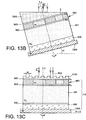
- FIG. 13B represents another example of a device according to the invention which differs from that of FIG. 13A in that, the optical system is a prism 1000 cut at an angle ⁇ .
- the prism 1000 is fixed relative to an assembly 1301 constituted by the mask 603, the photosensitive resin layer 601, the substrate 600 and the plate 1300.
- the plate 1300 is able to adopt an angle of inclination ⁇ substantially equal to ⁇ and to turn on itself, so as to turn the whole 1201 on itself. Tilting the plate 1300 by an angle ⁇ substantially equal to the angle ⁇ makes it possible to have a beam of light 602 that is normal to the prism 1000 and to expose the photoresist layer 601 with the maximum luminous intensity.
- the prism 1000 is formed of the same material as the mask 603, for example of a polymer-based material and is attached to the mask 603.
- the prism has a refractive index N equal to the refractive index N 1 of the mask.
- the prism 1000 is cut at an angle ⁇ which makes it possible to deflect the light beam 602, a predetermined deflection angle D, which is a function of the air index N 0 , the refractive index of the light. N prism, and angle ⁇ .
- the device of FIG. 13B also differs from that of FIG. 13A in that it comprises a first index matching layer 800 situated between the photoresist layer 601 and the mask 603. and which has a refractive index N 3 .
- the first index matching layer 800 is for example water or a fatty liquid such as glycerine whose refractive index N 3 is close to that N 1 of the mask and that N 2 of the resin layer This first index matching layer 800 minimizes the Fresnel reflections between the mask 603 and the photosensitive resin layer 601.
- the device of FIG. 13B also differs from that of FIG. 13A in that it further comprises a second index matching layer 900 having an index of refraction N 4 .
- the second index matching layer 900 is for example water or a fatty fluid such as glycerine.
- the second index matching layer 900 is located between the mask 603 and the optical system 606.
- the second index matching layer 900 has an index of refraction N 4 close to the index N of the optical system 606 and of the index N 1 of the mask 603.
- index matching layers 800 and 900 makes it possible, by minimizing the presence of air between the optical system 606 and the mask 603, on the one hand, and between the mask 603 and the resistor layer 601, on the other hand on the other hand, to obtain angles of inclination of the flanks of the resin patterns higher than those obtained in the prior art.
- the device of FIG. 13B finally differs from that of FIG. 13A in that it comprises an absorbent light-ray layer 700 situated between the substrate 600 and the photoresist layer 601.
- the absorbent ray layer 700 is used to prevent ultraviolet rays from reflecting on the substrate in the case where the beam of light rays 602 is from an ultraviolet light source.
- the light-absorbing layer 700 may be formed of a single layer or a stack of underlays.
- the absorbent layer of light rays 700 may be for example a resin mixed with carbon pigments.
- FIG. 13C represents another example of a device according to the invention that differs from that of FIG. 13B in that the optical system is a diffraction grating 1100. Moreover, the diffraction grating 1100 is mobile relative to a first one. 1301 assembly formed by the mask 603, the photosensitive resin layer 601, the substrate 600 and the plate 1300. Finally, the plate 1300 has a zero inclination angle ⁇ . He is able to turn on himself.
- FIG. 13D represents another example of a device according to the invention that differs from that of FIG. 13A in that the optical system is an optical diffuser 1200.
- the optical diffuser 1200, the mask 603, the photoresist layer 601, the substrate 600, and the plate 1300 form a second assembly 1302 rotatable on itself and movable relative to the light beam 602.
- the device also differs in that the mask 603, for example an etched chromium layer, is directly integrated with the photoresist layer 601.
- the index of the mask N 1 is equal to that of the resin N 2
- Le device also comprises an absorbent layer of light rays 700, located between the substrate 600 and the photosensitive resin layer 601 and an index matching layer 900 which has a refractive index N 4 .
- the plate 1300 has a zero inclination angle.
- FIG. 13E represents another example of a device according to the invention which differs from that of FIG. 13A in that the optical system is a network of micro-prisms 1111.
- the network of micro-prisms 1111 associated with the mask 603 form a third assembly 1303 capable of rotating on itself with respect to the photosensitive resin layer 601 to the substrate 600 and to the plate 1300.
- the third assembly 1303 is also movable relative to the light beam 602.
- the plate 1300 has a angle of inclination ⁇ zero.
Landscapes
- Engineering & Computer Science (AREA)
- Manufacturing & Machinery (AREA)
- Chemical & Material Sciences (AREA)
- Analytical Chemistry (AREA)
- Microelectronics & Electronic Packaging (AREA)
- Physics & Mathematics (AREA)
- General Physics & Mathematics (AREA)
- Exposure And Positioning Against Photoresist Photosensitive Materials (AREA)
- Photosensitive Polymer And Photoresist Processing (AREA)
Claims (20)
- Verfahren zur Herstellung von einem oder mehreren Mustern mittels Fotolithographie, das die folgenden Schritte umfasst:a) Abscheiden einer Fotoresistschicht (601) auf einem Substrat (600),
wobei das Verfahren dadurch gekennzeichnet ist, dass es die folgenden Schritte umfasst:b) Belichten der Fotoresistschicht (601) mittels eines Lichtstrahlenbündels (602) mit einer Hauptrichtung

 c) Entfernen bzw. Rückätzen der Maske (603),d) Entwickeln der Fotoresistschicht (601), um Muster mit Flanken herzustellen, die in Abhängigkeit von dem vorher festgelegten Ablenkwinkel (D̂) geneigt sind in Bezug auf eine Normale (n̂) zur Hauptebene des Substrats (600).
 - Verfahren nach Anspruch 1, dadurch gekennzeichnet, dass dem Schritt zur Abscheidung der Fotoresistschicht (601) ein Schritt zur Abscheidung von wenigstens einer Absorptionsschicht (700) der Lichtstrahlen vorausgeht.
- Verfahren nach einem der Ansprüche 1 oder 2, dadurch gekennzeichnet, dass nach dem Schritt a) zum Abscheiden der Fotoresistschicht (601) auf der Fotoresistschicht (601) eine Indexanpassungsschicttt (800) abgeschieden wird.
- Verfahren nach einem der Ansprüche 1 bis 3, dadurch gekennzeichnet, dass vor dem Belichtungsschritt der Fotoresistschicht (601) zwischen dem optischen System (606) und der Maske (603) eine Indexanpassungsschicht (900) realisiert wird.
- Verfahren nach einem der Ansprüche 1 bis 4, dadurch gekennzeichnet, dass das optische System (606) ein Prisma (1000), ein Beugungsgitter (1100), einen optischen Diffusor (1200) oder ein Mikroprismengitter (1111) umfasst.
- Verfahren nach einem der Ansprüche 1 bis 5, dadurch gekennzeichnet, dass während des Belichtungsschritts b) der Einfallwinkel (Î1) auf die Maske (603) variiert.
- Verfahren nach einem der Ansprüche 1 bis 6, dadurch gekennzeichnet, dass während des Belichtungsschritts b) einerseits das optische System (606) und andererseits das Substrat (600) in gegenseitige Relativbewegungen versetzt werden, wobei die Maske (603) entweder mit dem optischen System (606) oder mit dem Substrat (600) verbunden ist.
- Verfahren nach einem der Ansprüche 1 bis 6, dadurch gekennzeichnet, dass während des Belichtungsschritts b) eine durch das optische System (606), die Maske (603) und das Substrat (600) gebildete Einheit in eine Relativbewegung in Bezug auf das Lichtstrahlenbündel (602) versetzt wird.
- Vorrichtung zur Herstellung von einem oder von mehreren geneigten Mustern mittels Fotolithographie, ein Substrat (600) umfassend, auf dem eine Fotoresistschicht (601) mit einem Brechindex (N2) ruht, dadurch gekennzeichnet, dass sie außerdem eine Maske (603) mit Brechindex (N1), verbunden mit der genannten Fotoresistschicht oder mit einer auf der genannten Fotoresistschicht ruhenden Indexanpassungsschicht, ein optisches System (606), verbunden mit der Maske oder mit einer auf der Maske ruhenden Indexanpassungsschicht und Einrichtungen zum Belichten der Fotoresistschicht (601) mit Hilfe eines Lichtstrahlenbündels (602) mit der Hauptrichtung


- Vorrichtung nach Anspruch 9, bei der die Maske (603) eine oder mehrere Öffnungen (605) aufweist, dadurch gekennzeichnet, dass das optische System (606) und die Öffnungen (605) der Maske (603) ähnliche Brechindizes haben.
- Vorrichtung nach Anspruch 9, bei der die Maske (603) eine oder mehrere Öffnungen (605) aufweist, dadurch gekennzeichnet, dass das optische System (606) und die Öffnungen (605) der Maske (603) in dem gleichen Material realisiert sind.
- Vorrichtung nach einem der Ansprüche 9 bis 11, dadurch gekennzeichnet, dass die Maske (603) in die Fotoresistschicht (601) integriert ist.
- Vorrichtung nach einem der Ansprüche 9 bis 12, dadurch gekennzeichnet, dass das optische System (606) ein Prisma (1000), ein Beugungsgitter (1100), ein Mikroprismengitter (1111) oder einen optischen Diffusor (1200) umfasst.
- Vorrichtung nach einem der Ansprüche 9 bis 13, dadurch gekennzeichnet, dass sie eine Indexanpassungsschicht (800) zwischen der Fotoresistschicht (601) und der Maske (603) umfasst.
- Vorrichtung nach einem der Ansprüche 9 bis 14, dadurch gekennzeichnet, dass die Vorrichtung eine Indexanpassungsschicht (900) zwischen dem optischen System (606) und der Maske (603) umfasst.
- Vorrichtung nach einem der Ansprüche 14 oder 15, dadurch gekennzeichnet, dass die Anpassungsschicht (800) zwischen der Fotoresistschicht (601) und der Maske (603) und/oder die Anpassungsschicht (900) zwischen dem optischen System (606) und der Maske (603) eine Flüssigkeit wie Wasser oder ein fettes Fluid ist.
- Vorrichtung nach einem der Ansprüche 9 bis 16, dadurch gekennzeichnet, dass sie eine Lichtstrahlen absorbierende Schicht (700) zwischen dem Substrat (600) und der Fotoresistschicht (601) umfasst.
- Vorrichtung nach einem der Ansprüche 9 bis 17, dadurch gekennzeichnet, dass das optische System (606) in Bezug auf das Substrat (600) beweglich ist, wobei die Maske (603) entweder mit dem optischen System (606) oder dem Substrat (600) verbunden ist.
- Vorrichtung nach einem der Ansprüche 9 bis 18, dadurch gekennzeichnet, dass sie eine in Bezug auf das Lichtstrahlenbündel (602) drehbare Grundplatte (1300) umfasst, auf der das Substrat (600) ruht.
- Vorrichtung nach einem der Ansprüche 9 bis 19, dadurch gekennzeichnet, dass sie eine in Bezug auf das Lichtstrahlenbündel (602) neigbare Grundplatte (1300) umfasst, auf der das Substrat (600) ruht.
Applications Claiming Priority (2)
| Application Number | Priority Date | Filing Date | Title |
|---|---|---|---|
| FR0350410A FR2858694B1 (fr) | 2003-08-07 | 2003-08-07 | Procede de realisation de motifs a flancs inclines par photolithographie |
| PCT/FR2004/050377 WO2005017623A2 (fr) | 2003-08-07 | 2004-08-05 | Procede de realisation de motifs a flancs inclines par photolithographie |
Publications (2)
| Publication Number | Publication Date |
|---|---|
| EP1652009A2 EP1652009A2 (de) | 2006-05-03 |
| EP1652009B1 true EP1652009B1 (de) | 2007-03-07 |
Family
ID=34073135
Family Applications (1)
| Application Number | Title | Priority Date | Filing Date |
|---|---|---|---|
| EP04786375A Expired - Lifetime EP1652009B1 (de) | 2003-08-07 | 2004-08-05 | Verfahren zur herstellung von mustern mit geneigten flanken mittels fotolithographie |
Country Status (6)
| Country | Link |
|---|---|
| US (1) | US20070003839A1 (de) |
| EP (1) | EP1652009B1 (de) |
| JP (1) | JP2007501951A (de) |
| DE (1) | DE602004005210T2 (de) |
| FR (1) | FR2858694B1 (de) |
| WO (1) | WO2005017623A2 (de) |
Cited By (2)
| Publication number | Priority date | Publication date | Assignee | Title |
|---|---|---|---|---|
| WO2017220930A1 (fr) * | 2016-06-21 | 2017-12-28 | H.E.F. | Systeme et methode de realisation d'un masque optique pour micro-texturation de surface, installation et methode de micro-texturation de surface |
| EP4474909A1 (de) | 2023-06-01 | 2024-12-11 | Mimotec S.A. | Verfahren zur herstellung eines mikroformteils und mikromechanischer bauteile, sowie nach dem verfahren hergestellte mikromechanische bauteile |
Families Citing this family (23)
| Publication number | Priority date | Publication date | Assignee | Title |
|---|---|---|---|---|
| JP4911682B2 (ja) * | 2006-07-20 | 2012-04-04 | 富士フイルム株式会社 | 露光装置 |
| JP5070764B2 (ja) * | 2006-08-18 | 2012-11-14 | 凸版印刷株式会社 | マイクロニードルのパッチの製造方法 |
| JP4984736B2 (ja) * | 2006-08-18 | 2012-07-25 | 凸版印刷株式会社 | 露光装置及び方法 |
| WO2008020631A1 (en) * | 2006-08-18 | 2008-02-21 | Toppan Printing Co., Ltd. | Method for producing original plate, method for producing microneedle patch, microneedle patch, and exposure apparatus |
| JP2009151257A (ja) * | 2007-12-24 | 2009-07-09 | Ind Technol Res Inst | 傾斜露光リソグラフシステム |
| JP5194925B2 (ja) * | 2008-03-25 | 2013-05-08 | オムロン株式会社 | レジスト露光方法 |
| TW201015230A (en) | 2008-10-03 | 2010-04-16 | Univ Nat Chiao Tung | Immersion inclined lithography apparatus and tank thereof |
| JP5458241B2 (ja) * | 2009-10-14 | 2014-04-02 | 国立大学法人京都大学 | 微細構造体の作製方法 |
| US8367307B2 (en) * | 2010-02-05 | 2013-02-05 | GM Global Technology Operations LLC | Solution to optical constraint on microtruss processing |
| CN102566290B (zh) * | 2010-12-22 | 2014-06-18 | 上海微电子装备有限公司 | 投影式斜坡曝光光刻机装置与方法 |
| CN102540748B (zh) * | 2010-12-22 | 2014-11-12 | 上海微电子装备有限公司 | 投影式斜坡曝光光刻机装置与方法 |
| JP5798351B2 (ja) * | 2011-03-28 | 2015-10-21 | セイコーインスツル株式会社 | 電鋳型 |
| CN103034047B (zh) * | 2011-09-29 | 2014-10-29 | 上海微电子装备有限公司 | 一种提高分辨率的光刻工艺 |
| KR102160695B1 (ko) * | 2013-05-10 | 2020-09-29 | 삼성디스플레이 주식회사 | 마스크 |
| WO2014201414A1 (en) * | 2013-06-14 | 2014-12-18 | The Trustees Of Dartmouth College | Methods for fabricating magnetic devices and associated systems and devices |
| DE102015202121B4 (de) * | 2015-02-06 | 2017-09-14 | Infineon Technologies Ag | SiC-basierte Supersperrschicht-Halbleitervorrichtungen und Verfahren zur Herstellung dieser |
| CN104635435A (zh) * | 2015-02-10 | 2015-05-20 | 合肥工业大学 | 一种用于加工交叉网状微结构的光学组件 |
| DE102016110523B4 (de) | 2016-06-08 | 2023-04-06 | Infineon Technologies Ag | Verarbeiten einer Leistungshalbleitervorrichtung |
| CN107463063A (zh) * | 2017-08-02 | 2017-12-12 | 深圳市华星光电技术有限公司 | 紫外光固化掩膜板及其制作方法和固化方法 |
| US11644757B2 (en) * | 2019-12-19 | 2023-05-09 | Intel Corporation | Method to achieve tilted patterning with a through resist thickness using projection optics |
| CN116635787A (zh) | 2020-11-30 | 2023-08-22 | 应用材料公司 | 用以形成具倾斜角的结构的平版印刷术方法 |
| JP7812834B2 (ja) * | 2021-02-26 | 2026-02-10 | 富士フイルム株式会社 | フレキソ印刷版の製造方法 |
| JP2024527134A (ja) * | 2021-08-02 | 2024-07-19 | ロレックス・ソシエテ・アノニム | 時計部品の製造方法 |
Family Cites Families (6)
| Publication number | Priority date | Publication date | Assignee | Title |
|---|---|---|---|---|
| DE2411926A1 (de) * | 1974-03-13 | 1975-09-25 | Ibm Deutschland | Vorrichtung zum belichten lichtempfindlicher schichten durch masken |
| JPS57200042A (en) * | 1981-06-02 | 1982-12-08 | Hoya Corp | Exposure method for chemically machinable photosensitive glass |
| DE3842354A1 (de) * | 1988-12-16 | 1990-06-21 | Kernforschungsz Karlsruhe | Verfahren zur lithographischen herstellung von galvanisch abformbaren mikrostrukturen mit dreieckigem oder trapezfoermigem querschnitt |
| US4912022A (en) * | 1988-12-27 | 1990-03-27 | Motorola, Inc. | Method for sloping the profile of an opening in resist |
| DE19652463C2 (de) * | 1996-12-17 | 1999-02-25 | Univ Schiller Jena | Verfahren und Vorrichtung zur Herstellung dreidimensionaler Mikrostrukturen beliebiger Form |
| JPH11327154A (ja) * | 1998-05-13 | 1999-11-26 | Mitsubishi Electric Corp | 立体形状マイクロ部品の製造方法 |
-
2003
- 2003-08-07 FR FR0350410A patent/FR2858694B1/fr not_active Expired - Fee Related
-
2004
- 2004-08-05 EP EP04786375A patent/EP1652009B1/de not_active Expired - Lifetime
- 2004-08-05 JP JP2006522383A patent/JP2007501951A/ja active Pending
- 2004-08-05 WO PCT/FR2004/050377 patent/WO2005017623A2/fr not_active Ceased
- 2004-08-05 DE DE602004005210T patent/DE602004005210T2/de not_active Expired - Lifetime
- 2004-08-05 US US10/567,889 patent/US20070003839A1/en not_active Abandoned
Non-Patent Citations (1)
| Title |
|---|
| None * |
Cited By (3)
| Publication number | Priority date | Publication date | Assignee | Title |
|---|---|---|---|---|
| WO2017220930A1 (fr) * | 2016-06-21 | 2017-12-28 | H.E.F. | Systeme et methode de realisation d'un masque optique pour micro-texturation de surface, installation et methode de micro-texturation de surface |
| KR20190026674A (ko) * | 2016-06-21 | 2019-03-13 | 에이치.이.에프. | 표면 마이크로텍스쳐링을 위한 광학 마스크를 제조하기 위한 시스템 및 방법, 및 표면 마이크로텍스쳐링 설비 및 방법 |
| EP4474909A1 (de) | 2023-06-01 | 2024-12-11 | Mimotec S.A. | Verfahren zur herstellung eines mikroformteils und mikromechanischer bauteile, sowie nach dem verfahren hergestellte mikromechanische bauteile |
Also Published As
| Publication number | Publication date |
|---|---|
| FR2858694A1 (fr) | 2005-02-11 |
| WO2005017623A3 (fr) | 2005-10-06 |
| DE602004005210T2 (de) | 2007-11-22 |
| FR2858694B1 (fr) | 2006-08-18 |
| DE602004005210D1 (de) | 2007-04-19 |
| EP1652009A2 (de) | 2006-05-03 |
| US20070003839A1 (en) | 2007-01-04 |
| WO2005017623A2 (fr) | 2005-02-24 |
| JP2007501951A (ja) | 2007-02-01 |
Similar Documents
| Publication | Publication Date | Title |
|---|---|---|
| EP1652009B1 (de) | Verfahren zur herstellung von mustern mit geneigten flanken mittels fotolithographie | |
| US7455957B2 (en) | Blazed holographic grating, method for producing the same and replica grating | |
| JP2920164B2 (ja) | 複製回折格子のための反射性保護膜 | |
| JP2007523468A (ja) | 3次元ナノスケール構造を形成するための方法及び装置 | |
| FR2474708A1 (fr) | Procede de microphotolithographie a haute resolution de traits | |
| US10768349B2 (en) | Reflective diffraction grating and fabrication method | |
| US20090170038A1 (en) | Method for producing fine structure | |
| CN1950680A (zh) | 光散射euvl掩模 | |
| KR100990074B1 (ko) | 경사 노광 리소그래피 시스템 | |
| WO2001009680A1 (fr) | Structure pour masque de lithographie en reflexion et procede pour sa realisation | |
| EP1960835B1 (de) | Reflexionsmaske für die lithographie und verfahren zu ihrer herstellung | |
| FR2738670A1 (fr) | Procede et appareil de formation d'un motif sur un substrat de circuit integre | |
| US20040121527A1 (en) | A Method Of Structuring Of A Substrate | |
| US20260016744A1 (en) | Nanoshape patterning techniques that allow high-throughput fabrication of functional nanostructures with complex geometries on planar and non-planar substrates | |
| WO2007068617A1 (fr) | Procede de fabrication de masque lithographique en reflexion et masque issu du procede | |
| EP1803031B1 (de) | Reflektierende lithographiemaske und verfahren zu deren herstellung | |
| EP3655821B1 (de) | Interferenzlithographie -verfahren und -system | |
| US7924489B2 (en) | Hidden micromirror support structure | |
| FR2878983A1 (fr) | Dispositif et procede de photolithographie ameliores permettant la realisation de motifs a flancs inclines | |
| FR3161291A1 (fr) | Procédé de fabrication d'une structure hiérarchique micro-nanométrique et structure hiérarchique micro-nanométrique obtenu par un tel procédé | |
| Cardoso | Development of resonant nanostructures large area device for augmented reality | |
| EP1880249B1 (de) | Optisches system für eine lithographievorrichtung | |
| JP2009151257A (ja) | 傾斜露光リソグラフシステム | |
| WO2001053891A1 (fr) | Procede de lithographie ionique, revetement a fort contraste, equipement et reticule de mise en oeuvre | |
| FR3007151A1 (fr) | Procede de fabrication d'un masque de lithographie uv par contact et de puces optoelectroniques au moyen d'un tel masque |
Legal Events
| Date | Code | Title | Description |
|---|---|---|---|
| PUAI | Public reference made under article 153(3) epc to a published international application that has entered the european phase |
Free format text: ORIGINAL CODE: 0009012 |
|
| 17P | Request for examination filed |
Effective date: 20060203 |
|
| AK | Designated contracting states |
Kind code of ref document: A2 Designated state(s): AT BE BG CH CY CZ DE DK EE ES FI FR GB GR HU IE IT LI LU MC NL PL PT RO SE SI SK TR |
|
| AX | Request for extension of the european patent |
Extension state: AL HR LT LV MK |
|
| RBV | Designated contracting states (corrected) |
Designated state(s): CH DE FR GB IT LI |
|
| RTI1 | Title (correction) |
Free format text: METHOD FOR PRODUCING PATTERNS WITH INCLINED SIDEWALLS BY PHOTOLITHOGRAPHY |
|
| GRAP | Despatch of communication of intention to grant a patent |
Free format text: ORIGINAL CODE: EPIDOSNIGR1 |
|
| RAP1 | Party data changed (applicant data changed or rights of an application transferred) |
Owner name: COMMISSARIAT A L'ENERGIE ATOMIQUE |
|
| DAX | Request for extension of the european patent (deleted) | ||
| RBV | Designated contracting states (corrected) |
Designated state(s): CH DE FR GB IT LI |
|
| GRAS | Grant fee paid |
Free format text: ORIGINAL CODE: EPIDOSNIGR3 |
|
| GRAA | (expected) grant |
Free format text: ORIGINAL CODE: 0009210 |
|
| AK | Designated contracting states |
Kind code of ref document: B1 Designated state(s): CH DE FR GB IT LI |
|
| REG | Reference to a national code |
Ref country code: GB Ref legal event code: FG4D Free format text: NOT ENGLISH |
|
| REG | Reference to a national code |
Ref country code: CH Ref legal event code: EP |
|
| REF | Corresponds to: |
Ref document number: 602004005210 Country of ref document: DE Date of ref document: 20070419 Kind code of ref document: P |
|
| GBT | Gb: translation of ep patent filed (gb section 77(6)(a)/1977) |
Effective date: 20070523 |
|
| PLBE | No opposition filed within time limit |
Free format text: ORIGINAL CODE: 0009261 |
|
| STAA | Information on the status of an ep patent application or granted ep patent |
Free format text: STATUS: NO OPPOSITION FILED WITHIN TIME LIMIT |
|
| RAP2 | Party data changed (patent owner data changed or rights of a patent transferred) |
Owner name: MIMOTEC S.A. |
|
| 26N | No opposition filed |
Effective date: 20071210 |
|
| REG | Reference to a national code |
Ref country code: CH Ref legal event code: NV Representative=s name: LEMAN CONSULTING S.A. Ref country code: CH Ref legal event code: PUE Owner name: MIMOTEC S.A. Free format text: COMMISSARIAT A L'ENERGIE ATOMIQUE#25, RUE LEBLANC IMMEUBLE "LE PONANT D"#75015 PARIS (FR) -TRANSFER TO- MIMOTEC S.A.#RUE BLANCHERIE 61#1950 SION (CH) |
|
| REG | Reference to a national code |
Ref country code: FR Ref legal event code: TP |
|
| GBPC | Gb: european patent ceased through non-payment of renewal fee |
Effective date: 20080805 |
|
| PG25 | Lapsed in a contracting state [announced via postgrant information from national office to epo] |
Ref country code: GB Free format text: LAPSE BECAUSE OF NON-PAYMENT OF DUE FEES Effective date: 20080805 |
|
| REG | Reference to a national code |
Ref country code: CH Ref legal event code: PCOW Free format text: MIMOTEC S.A.;ROUTE DES ILES 20;1950 SION (CH) |
|
| PGFP | Annual fee paid to national office [announced via postgrant information from national office to epo] |
Ref country code: IT Payment date: 20070831 Year of fee payment: 4 |
|
| PGFP | Annual fee paid to national office [announced via postgrant information from national office to epo] |
Ref country code: CH Payment date: 20140820 Year of fee payment: 11 Ref country code: DE Payment date: 20140821 Year of fee payment: 11 |
|
| PGFP | Annual fee paid to national office [announced via postgrant information from national office to epo] |
Ref country code: FR Payment date: 20140821 Year of fee payment: 11 |
|
| REG | Reference to a national code |
Ref country code: DE Ref legal event code: R082 Ref document number: 602004005210 Country of ref document: DE |
|
| REG | Reference to a national code |
Ref country code: DE Ref legal event code: R119 Ref document number: 602004005210 Country of ref document: DE |
|
| REG | Reference to a national code |
Ref country code: CH Ref legal event code: PL |
|
| PG25 | Lapsed in a contracting state [announced via postgrant information from national office to epo] |
Ref country code: CH Free format text: LAPSE BECAUSE OF NON-PAYMENT OF DUE FEES Effective date: 20150831 Ref country code: LI Free format text: LAPSE BECAUSE OF NON-PAYMENT OF DUE FEES Effective date: 20150831 |
|
| REG | Reference to a national code |
Ref country code: FR Ref legal event code: ST Effective date: 20160429 |
|
| PG25 | Lapsed in a contracting state [announced via postgrant information from national office to epo] |
Ref country code: DE Free format text: LAPSE BECAUSE OF NON-PAYMENT OF DUE FEES Effective date: 20160301 |
|
| PG25 | Lapsed in a contracting state [announced via postgrant information from national office to epo] |
Ref country code: FR Free format text: LAPSE BECAUSE OF NON-PAYMENT OF DUE FEES Effective date: 20150831 |