EP3655986B1 - Ensemble cathode ayant un magnétron à double position et un agent de refroidissement à alimentation centrale - Google Patents
Ensemble cathode ayant un magnétron à double position et un agent de refroidissement à alimentation centrale Download PDFInfo
- Publication number
- EP3655986B1 EP3655986B1 EP18834519.3A EP18834519A EP3655986B1 EP 3655986 B1 EP3655986 B1 EP 3655986B1 EP 18834519 A EP18834519 A EP 18834519A EP 3655986 B1 EP3655986 B1 EP 3655986B1
- Authority
- EP
- European Patent Office
- Prior art keywords
- assembly
- target
- rotatable magnet
- magnetron
- magnet assembly
- Prior art date
- Legal status (The legal status is an assumption and is not a legal conclusion. Google has not performed a legal analysis and makes no representation as to the accuracy of the status listed.)
- Active
Links
Images

Classifications
-
- H—ELECTRICITY
- H01—ELECTRIC ELEMENTS
- H01J—ELECTRIC DISCHARGE TUBES OR DISCHARGE LAMPS
- H01J37/00—Discharge tubes with provision for introducing objects or material to be exposed to the discharge, e.g. for the purpose of examination or processing thereof
- H01J37/32—Gas-filled discharge tubes
- H01J37/34—Gas-filled discharge tubes operating with cathodic sputtering
- H01J37/3411—Constructional aspects of the reactor
- H01J37/345—Magnet arrangements in particular for cathodic sputtering apparatus
- H01J37/3455—Movable magnets
-
- C—CHEMISTRY; METALLURGY
- C23—COATING METALLIC MATERIAL; COATING MATERIAL WITH METALLIC MATERIAL; CHEMICAL SURFACE TREATMENT; DIFFUSION TREATMENT OF METALLIC MATERIAL; COATING BY VACUUM EVAPORATION, BY SPUTTERING, BY ION IMPLANTATION OR BY CHEMICAL VAPOUR DEPOSITION, IN GENERAL; INHIBITING CORROSION OF METALLIC MATERIAL OR INCRUSTATION IN GENERAL
- C23C—COATING METALLIC MATERIAL; COATING MATERIAL WITH METALLIC MATERIAL; SURFACE TREATMENT OF METALLIC MATERIAL BY DIFFUSION INTO THE SURFACE, BY CHEMICAL CONVERSION OR SUBSTITUTION; COATING BY VACUUM EVAPORATION, BY SPUTTERING, BY ION IMPLANTATION OR BY CHEMICAL VAPOUR DEPOSITION, IN GENERAL
- C23C14/00—Coating by vacuum evaporation, by sputtering or by ion implantation of the coating forming material
- C23C14/22—Coating by vacuum evaporation, by sputtering or by ion implantation of the coating forming material characterised by the process of coating
- C23C14/34—Sputtering
- C23C14/3407—Cathode assembly for sputtering apparatus, e.g. Target
-
- C—CHEMISTRY; METALLURGY
- C23—COATING METALLIC MATERIAL; COATING MATERIAL WITH METALLIC MATERIAL; CHEMICAL SURFACE TREATMENT; DIFFUSION TREATMENT OF METALLIC MATERIAL; COATING BY VACUUM EVAPORATION, BY SPUTTERING, BY ION IMPLANTATION OR BY CHEMICAL VAPOUR DEPOSITION, IN GENERAL; INHIBITING CORROSION OF METALLIC MATERIAL OR INCRUSTATION IN GENERAL
- C23C—COATING METALLIC MATERIAL; COATING MATERIAL WITH METALLIC MATERIAL; SURFACE TREATMENT OF METALLIC MATERIAL BY DIFFUSION INTO THE SURFACE, BY CHEMICAL CONVERSION OR SUBSTITUTION; COATING BY VACUUM EVAPORATION, BY SPUTTERING, BY ION IMPLANTATION OR BY CHEMICAL VAPOUR DEPOSITION, IN GENERAL
- C23C14/00—Coating by vacuum evaporation, by sputtering or by ion implantation of the coating forming material
- C23C14/22—Coating by vacuum evaporation, by sputtering or by ion implantation of the coating forming material characterised by the process of coating
- C23C14/34—Sputtering
- C23C14/3435—Applying energy to the substrate during sputtering
- C23C14/345—Applying energy to the substrate during sputtering using substrate bias
-
- C—CHEMISTRY; METALLURGY
- C23—COATING METALLIC MATERIAL; COATING MATERIAL WITH METALLIC MATERIAL; CHEMICAL SURFACE TREATMENT; DIFFUSION TREATMENT OF METALLIC MATERIAL; COATING BY VACUUM EVAPORATION, BY SPUTTERING, BY ION IMPLANTATION OR BY CHEMICAL VAPOUR DEPOSITION, IN GENERAL; INHIBITING CORROSION OF METALLIC MATERIAL OR INCRUSTATION IN GENERAL
- C23C—COATING METALLIC MATERIAL; COATING MATERIAL WITH METALLIC MATERIAL; SURFACE TREATMENT OF METALLIC MATERIAL BY DIFFUSION INTO THE SURFACE, BY CHEMICAL CONVERSION OR SUBSTITUTION; COATING BY VACUUM EVAPORATION, BY SPUTTERING, BY ION IMPLANTATION OR BY CHEMICAL VAPOUR DEPOSITION, IN GENERAL
- C23C14/00—Coating by vacuum evaporation, by sputtering or by ion implantation of the coating forming material
- C23C14/22—Coating by vacuum evaporation, by sputtering or by ion implantation of the coating forming material characterised by the process of coating
- C23C14/34—Sputtering
- C23C14/35—Sputtering by application of a magnetic field, e.g. magnetron sputtering
-
- H—ELECTRICITY
- H01—ELECTRIC ELEMENTS
- H01J—ELECTRIC DISCHARGE TUBES OR DISCHARGE LAMPS
- H01J37/00—Discharge tubes with provision for introducing objects or material to be exposed to the discharge, e.g. for the purpose of examination or processing thereof
- H01J37/32—Gas-filled discharge tubes
- H01J37/34—Gas-filled discharge tubes operating with cathodic sputtering
- H01J37/3402—Gas-filled discharge tubes operating with cathodic sputtering using supplementary magnetic fields
- H01J37/3405—Magnetron sputtering
-
- H—ELECTRICITY
- H01—ELECTRIC ELEMENTS
- H01J—ELECTRIC DISCHARGE TUBES OR DISCHARGE LAMPS
- H01J37/00—Discharge tubes with provision for introducing objects or material to be exposed to the discharge, e.g. for the purpose of examination or processing thereof
- H01J37/32—Gas-filled discharge tubes
- H01J37/34—Gas-filled discharge tubes operating with cathodic sputtering
- H01J37/3402—Gas-filled discharge tubes operating with cathodic sputtering using supplementary magnetic fields
- H01J37/3405—Magnetron sputtering
- H01J37/3408—Planar magnetron sputtering
-
- H—ELECTRICITY
- H01—ELECTRIC ELEMENTS
- H01J—ELECTRIC DISCHARGE TUBES OR DISCHARGE LAMPS
- H01J37/00—Discharge tubes with provision for introducing objects or material to be exposed to the discharge, e.g. for the purpose of examination or processing thereof
- H01J37/32—Gas-filled discharge tubes
- H01J37/34—Gas-filled discharge tubes operating with cathodic sputtering
- H01J37/3411—Constructional aspects of the reactor
- H01J37/3414—Targets
- H01J37/3426—Material
-
- H—ELECTRICITY
- H01—ELECTRIC ELEMENTS
- H01J—ELECTRIC DISCHARGE TUBES OR DISCHARGE LAMPS
- H01J37/00—Discharge tubes with provision for introducing objects or material to be exposed to the discharge, e.g. for the purpose of examination or processing thereof
- H01J37/32—Gas-filled discharge tubes
- H01J37/34—Gas-filled discharge tubes operating with cathodic sputtering
- H01J37/3411—Constructional aspects of the reactor
- H01J37/3435—Target holders (includes backing plates and endblocks)
-
- H—ELECTRICITY
- H01—ELECTRIC ELEMENTS
- H01J—ELECTRIC DISCHARGE TUBES OR DISCHARGE LAMPS
- H01J37/00—Discharge tubes with provision for introducing objects or material to be exposed to the discharge, e.g. for the purpose of examination or processing thereof
- H01J37/32—Gas-filled discharge tubes
- H01J37/34—Gas-filled discharge tubes operating with cathodic sputtering
- H01J37/3464—Operating strategies
- H01J37/347—Thickness uniformity of coated layers or desired profile of target erosion
-
- H—ELECTRICITY
- H01—ELECTRIC ELEMENTS
- H01J—ELECTRIC DISCHARGE TUBES OR DISCHARGE LAMPS
- H01J37/00—Discharge tubes with provision for introducing objects or material to be exposed to the discharge, e.g. for the purpose of examination or processing thereof
- H01J37/32—Gas-filled discharge tubes
- H01J37/34—Gas-filled discharge tubes operating with cathodic sputtering
- H01J37/3488—Constructional details of particle beam apparatus not otherwise provided for, e.g. arrangement, mounting, housing, environment; special provisions for cleaning or maintenance of the apparatus
- H01J37/3497—Temperature of target
Definitions
- Embodiments of the present disclosure generally relate to magnetrons for use in physical vapor deposition chambers for substrate processing.
- PVD physical vapor deposition
- TSV through silicon via
- the deposition rate in such applications decreases over the target life, thus also decreasing throughput of the chamber.
- the deposition rate decreases from 18 angstroms per second (A/s) to 12 A/s over the target life.
- Conventional methods of addressing the deposition rate decrease include changing the power to compensate for deposition rate decrease.
- changing the power is laborious and requires constant monitoring of the deposition rate of the chamber.
- Patent application US 2004/045670 A1 discloses a PVD chamber including a rotating magnetron having a set of magnets. The magnetron is coupled to a hollow drive shaft. The hollow drive shaft is coupled to a coolant delivery system.
- Patent application WO 2008/123987 A1 discloses a sputter chamber including a target and a magnetron. A mechanism allows vertical movement of the magnetron to optimize the distance between the magnetron and the back of the target.
- Patent application WO 02/47110 A1 discloses a sputtering apparatus including a target and a magnetron disposed adjacent the target, including at least one magnet assembly movable laterally and rotationally relative to the target. The patent application further discloses that the magnet assembly could be mounted for vertical movement.
- Patent application US 6 153 068 A discloses a sputtering device including a vessel, a means for introducing magnetic field, and a target. The means for introducing magnetic field is installed outside the vessel and can be moved in upward and downward directions and in rotational direction.
- Embodiments of a magnetron assembly according to claim 1 and a processing system incorporating same are provided herein.
- the present disclosure relates to a cathode assembly having a dual position magnetron that can advantageously improve cooling using centrally fed coolant and that can ensure a constant deposition rate by keeping the distance between the lowermost surface of the magnets of the magnetron and the lowermost surface of the sputtering target constant during deposition processes and physical vapor deposition (PVD) chambers incorporating such magnetrons.
- the inventive magnetron advantageously alleviates cracking and/or bowing of the target due to overheating and a decrease in the deposition rate over the life of the target.
- Embodiments of the magnetron disclosed herein have two positions (outer radial position and inner radial position), thus enabling a change in the magnetic field at the sputtering target surface by the reconfiguration of the magnet poles in the different positions. As such, target utilization is further improved because the center and periphery of the target are both sputtered.
- FIG. 1 depicts a simplified, cross-sectional view of a substrate processing system (e.g., physical vapor deposition (PVD) processing system 100) in accordance with some embodiments of the present disclosure.
- PVD physical vapor deposition
- Examples of other PVD chambers suitable for modification in accordance with the teachings provided herein include the VENTURA ® and SIP ENCORE ® PVD processing chambers, both commercially available from Applied Materials, Inc., of Santa Clara, California.
- Other processing chambers from Applied Materials, Inc. or other manufactures, including those configured for other types of processing besides PVD may also benefit from modifications in accordance with the teachings disclosed herein.
- the PVD processing system 100 includes a chamber lid 102 removably disposed atop a process chamber 104.
- the chamber lid 102 may include a target assembly 114 and a grounding assembly 103.
- the process chamber 104 contains a substrate support 106 for receiving a substrate 108 thereon.
- the substrate support 106 may be located within a lower grounded enclosure wall 110, which may be a chamber wall of the process chamber 104.
- the lower grounded enclosure wall 110 may be electrically coupled to the grounding assembly 103 of the chamber lid 102 such that an RF return path is provided to an RF power source 182 disposed above the chamber lid 102.
- the RF power source 182 may provide RF energy to the target assembly 114 as discussed below.
- a DC power source may be similarly coupled to target assembly 114
- the PVD processing system 100 may include a source distribution plate 158 opposing a backside of the target assembly 114 and electrically coupled to the target assembly 114 along a peripheral edge of the target assembly 114.
- the PVD processing system 100 may include a cavity 170 disposed between the backside of the target assembly 114 and the source distribution plate 158.
- the cavity 170 may at least partially house a magnetron assembly 196 as discussed below.
- the cavity 170 is at least partially defined by the inner surface of a conductive support ring 164, a target facing surface of the source distribution plate 158, and a source distribution plate facing surface ( e . g ., backside) of the target assembly 114 (or backing plate 160).
- the PVD processing system 100 further includes a magnetron assembly 196.
- the magnetron assembly 196 provides a rotating magnetic field proximate the target to assist in plasma processing within the process chamber 104.
- the magnetron assembly includes a rotatable magnet assembly 148 disposed within the cavity 170.
- the rotatable magnet assembly 148 rotates about a central axis 186 of the process chamber 104.
- the rotatable magnet assembly 148 provides two different closed magnetic field configurations that are selectable during use. In some embodiments, the configuration can be selected by rotating a section of the rotatable magnet assembly 148, as described below with respect to Figures 1 and 2 .
- the magnetron assembly 196 includes a body 154, a first motor 176, a coupling assembly 178 ( e . g ., a gear assembly) coupled to the first motor 176 and the body 154, a coolant feed structure 183, and the rotatable magnet assembly 148.
- the rotatable magnet assembly 148 includes a plurality of magnets 150 and is configured to rotate the plurality of magnets 150 about the central axis 186 and a magnet axis 286 as well as move the magnet assembly 148 vertically within the cavity 170, as described below.
- the magnetron assembly 196 further includes a second motor 177 coupled to the body 154 to control a vertical position of the body 154 (e.g., the body 154 may be a telescoping body).
- the first and second motors 176, 177 may be electric motors, pneumatic or hydraulic drives, or any other process-compatible mechanism that can provide the required movement. While one illustrative embodiment is described herein to illustrate how the rotatable magnet assembly 148 may be rotated, other configurations may also be used.
- the inventive magnetron assembly 196 is also capable of vertical movement to control the distance from the plurality of magnets 150 to the substrate-facing surface of the target assembly 114, for example, to ensure that the distance remains substantially constant.
- the magnetron assembly 196 rotates and, in some embodiments, vertically moves the rotatable magnet assembly 148 within the cavity 170.
- the first motor 176 and coupling assembly 178 may be provided to rotate the rotatable magnet assembly 148 while the second motor 177 moves the rotatable magnet assembly 148 in a vertical direction.
- the body 154 is fixedly coupled to the rotatable magnet assembly 148.
- the rotatable magnet assembly 148 is rotatably coupled to the coolant feed structure 183 to allow the rotatable magnet assembly 148 to rotate while the coolant feed structure remains stationary.
- the rotatable magnet assembly 148 is coupled to a bottom portion of the coolant feed structure 183 via a bearing 174.
- the coupling assembly 178 may be a belt that includes ridges which mate with grooves disposed in the first motor 176 and the body 154 to transfer the rotational motion provided by the first motor 176 to the rotatable magnet assembly 148.
- a similar motor (not shown) may be coupled to the plurality of magnets 150 to rotate the plurality of magnets 150 about the magnet axis 286, as discussed below.
- the coupling assembly 178 may alternatively be coupled to the rotatable magnet assembly 148 through the use of pulleys, gears, or other suitable means of transferring the rotational motion provided by the first motor 176.
- the coolant feed structure 183 which supplies coolant to a center of the target assembly 114 (i.e., along the central axis 186.
- the coolant feed structure 183 extends through the body 154 along the central axis 186.
- the coolant feed structure 183 includes a central channel 161 extending along the central axis 186 from a manifold portion 162 through a body portion 163.
- a coolant supply 165 is fluidly coupled to an inlet 167 of the manifold portion 162 to supply a coolant through the coolant feed structure 183 and into the cavity 170.
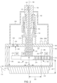
- Figure 2 depicts a schematic cross-sectional view of the magnetron assembly 196 in accordance with some embodiments of the present disclosure.
- the rotatable magnet assembly 148 can rotate the plurality of magnets 150 (as indicated by arrow 201) about the central axis 186 at a first distance (inner radial position) about the central axis 186 and at a second distance (outer radial position as depicted in Figure 2 ), which is greater than the first distance, from the central axis 186.
- the plurality of magnets 150 are also configured to rotate (as indicated by arrow 203) about the magnet axis 286 passing through a center of the plurality of magnets 150.
- a cover 226 may optionally be disposed atop the source distribution plate 158 around the portion of the magnetron assembly 196 that extends above the source distribution plate 158 exposing only the manifold portion 162.
- the magnetron assembly 196 may include two or more sensors (two sensors 204a, 204b shown in Figure 2 ) configured to determine whether the plurality of magnets 150 are rotating in the outer radial position or the inner radial position.
- the two sensors 204a, 204b are disposed atop the source distribution plate 158 at different radial positions.
- the rotatable magnet assembly 148 includes an indicating element 206 disposed atop the plurality of magnets 150.
- the two sensors 204a, 204b are arranged in a manner so that when a second sensor 204b detects the indicating element 206, the plurality of magnets 150 are being rotated about the central axis 186 at the outer radial position (as depicted in Figure 2 ) and when a first sensor204a detects the indicating element 206, the plurality of magnets 150 are being rotated about the central axis 186 at the inner radial position.
- a third sensor 212 may be disposed through the conductive support ring 164 to detect the movement of the plurality of magnets 150 and to detect the vertical position of the rotatable magnet assembly 148.
- the first motor 176 is configured to rotate the rotatable magnet assembly 148 at a first predetermined speed so that at a first speed, the plurality of magnets 150 rotate at the inner radial position and at a second predetermined speed, the plurality of magnets 150 rotate at the outer radial position.
- one or more stoppers 208 and a counterweight 210 may be utilized.
- the magnetron assembly 196 is configured to move the rotatable magnet assembly 148 in a vertical direction as indicated by arrow 205 to control a vertical distance 207 between a first lowermost surface 214 of the plurality of magnets 150 and a second lowermost surface 216 of the target assembly 114.
- the vertical distance 207 can be controlled to maintain the vertical distance 207 to be substantially constant through the life of the target.
- a decrease in deposition rate of the target is advantageously substantially reduced or eliminated.
- the body 154 is coupled directly to the rotatable magnet assembly 148 to transmit the movement of the second motor 177 to and vertically move the rotatable magnet assembly 148.
- the body 154 may be coupled to the source distribution plate 158 via bellows 218.
- the coolant feed structure 183 extends through the body 154 along the central axis 186 to supply a coolant (as shown by flow lines 220) to the cavity at a center of the target assembly 114.
- a coolant as shown by flow lines 220
- a more uniform flow of coolant is advantageously achieved, thus substantially reducing or eliminating the temperature gradient across the target assembly 114. Cracking and bowing of a source material 113 of the target assembly 114 is, therefore, also substantially reduced or eliminated.
- the coolant After entering the cavity 170 through the coolant feed structure 183, the coolant subsequently flows out of the cavity 170 through an opening 224 formed in an outlet 222 disposed in the source distribution plate 158.
- a return line (not shown) is coupled to the outlet 222 to receive the coolant after the coolant has flowed through the cavity 170.
- the substrate support 106 has a material-receiving surface facing a principal surface of a target assembly 114 and supports the substrate 108 to be sputter coated in planar position opposite to the principal surface of the target assembly 114.
- the substrate support 106 may support the substrate 108 in a central region 120 of the process chamber 104.
- the central region 120 is defined as the region above the substrate support 106 during processing (for example, between the target assembly 114 and the substrate support 106 when in a processing position).
- the substrate support 106 may be vertically movable to allow the substrate 108 to be transferred onto the substrate support 106 through a load lock valve (not shown) in the lower portion of the process chamber 104 and thereafter raised to a deposition, or processing position.
- a bellows 122 connected to a bottom chamber wall 124 may be provided to maintain a separation of the inner volume of the process chamber 104 from the atmosphere outside of the process chamber 104 while facilitating vertical movement of the substrate support 106.
- One or more gases may be supplied from a gas source 126 through a mass flow controller 128 into the lower part of the process chamber 104.
- An exhaust port 130 may be provided and coupled to a pump (not shown) via a valve 132 for exhausting the interior of the process chamber 104 and to facilitate maintaining a desired pressure inside the process chamber 104.
- An RF bias power source 134 may be coupled to the substrate support 106 in order to induce a negative DC bias on the substrate 108.
- a negative DC self-bias may form on the substrate 108 during processing.
- RF energy supplied by the RF bias power source 134 may range in frequency from about 2 MHz to about 60 MHz, for example, non-limiting frequencies such as 2 MHz, 13.56 MHz, or 60 MHz can be used.
- RF power may be supplied in a range from about 2 kW to about 20 kW.
- DC power may be supplied in range from about 2 kW to about 40 kW.
- the substrate support 106 may be grounded or left electrically floating.
- a capacitance tuner 136 may be coupled to the substrate support 106 for adjusting voltage on the substrate 108 for applications where RF bias power may not be desired.
- the process chamber 104 further includes a process kit shield, or shield, 138 to surround the processing volume, or central region, of the process chamber 104 and to protect other chamber components from damage and/or contamination from processing.
- the shield 138 may be connected to a ledge 140 of an upper grounded enclosure wall 116 of the process chamber 104.
- the chamber lid 102 may rest on the ledge 140 of the upper grounded enclosure wall 116.
- the upper grounded enclosure wall 116 may provide a portion of the RF return path between the lower grounded enclosure wall 116 and the grounding assembly 103 of the chamber lid 102.
- other RF return paths are possible, such as via the grounded shield 138.
- the shield 138 extends downwardly and may include a generally tubular portion having a generally constant diameter that generally surrounds the central region 120.
- the shield 138 extends along the walls of the upper grounded enclosure wall 116 and the lower grounded enclosure wall 110 downwardly to below a top surface of the substrate support 106 and returns upwardly until reaching a top surface of the substrate support 106 ( e.g ., forming a u-shaped portion at the bottom of the shield 138).
- a cover ring 146 rests on the top of an upwardly extending inner portion of the shield 138 when the substrate support 106 is in a lower, loading position but rests on the outer periphery of the substrate support 106 when in an upper, deposition position to protect the substrate support 106 from sputter deposition.
- An additional deposition ring (not shown) may be used to protect the edges of the substrate support 106 from deposition around the edge of the substrate 108.
- a magnet 152 may be disposed about the process chamber 104 for selectively providing a magnetic field between the substrate support 106 and the target assembly 114.
- the magnet 152 may be disposed about the outside of the enclosure wall 110 in a region just above the substrate support 106 when in processing position.
- the magnet 152 may be disposed additionally or alternatively in other locations, such as adjacent the upper grounded enclosure wall 116.
- the magnet 152 may be an electromagnet and may be coupled to a power source (not shown) for controlling the magnitude of the magnetic field generated by the electromagnet.
- the chamber lid 102 generally includes the grounding assembly 103 disposed about the target assembly 114.
- the grounding assembly 103 may include a grounding plate 156 having a first surface 157 that may be generally parallel to and opposite a backside of the target assembly 114.
- a grounding shield 112 may extending from the first surface 157 of the grounding plate 156 and surround the target assembly 114.
- the grounding assembly 103 may include a support member 175 to support the target assembly 114 within the grounding assembly 103.
- the support member 175 may be coupled to a lower end of the grounding shield 112 proximate an outer peripheral edge of the support member 175 and extends radially inward to support a seal ring 181, and the target assembly 114.
- the seal ring 181 may be a ring or other annular shape having a desired cross-section.
- the seal ring 181 may include two opposing planar and generally parallel surfaces to facilitate interfacing with the target assembly 114, such as the backing plate 160, on a first side of the seal ring 181 and with the support member 175 on a second side of the seal ring 181.
- the seal ring 181 may be made of a dielectric material, such as ceramic. The seal ring 181 may insulate the target assembly 114 from the ground assembly 103.
- the support member 175 may be a generally planar member having a central opening to accommodate the target assembly 114.
- the support member 175 may be circular, or disc-like in shape, although the shape may vary depending upon the corresponding shape of the chamber lid and/or the shape of the substrate to be processed in the PVD processing system 100.
- the target assembly 114 includes the source material 113 to be deposited on a substrate, such as the substrate 108 during sputtering, such as a metal, metal oxide, metal alloy, or the like.
- the source material 113 may be titanium, tantalum, tungsten, or the like.
- the target assembly 114 includes a backing plate 160 to support the source material 113.
- the source material 113 may be disposed on a substrate support facing side of the backing plate assembly 160 as illustrated in Figure 1 .
- the backing plate 160 may comprise a conductive material, such as copper-zinc, copper-chrome, or the same material as the target, such that RF and DC power can be coupled to the source material 113 via the backing plate 160.
- the backing plate 160 may be non-conductive and may include conductive elements (not shown) such as electrical feedthroughs or the like.
- the backing plate 160 may be disc shaped, rectangular, square, or any other shape that may be accommodated by the PVD processing system 100.
- the backing plate 160 is configured to support the source material 113 such that a front surface of the source material opposes the substrate 108 when present.
- the source material 113 may be coupled to the backing plate 160 in any suitable manner.
- the source material 113 may be diffusion bonded to the backing plate 160.
- the conductive support ring 164 may be disposed between the source distribution plate 158 and the backside of the target assembly 114 to propagate RF energy from the source distribution plate to the peripheral edge of the target assembly 114.
- the conductive support ring 164 may be cylindrical, with a first end 166 coupled to a target-facing surface of the source distribution plate 158 proximate the peripheral edge of the source distribution plate 158 and a second end 168 coupled to a source distribution plate-facing surface of the target assembly 114 proximate the peripheral edge of the target assembly 114.
- the second end 168 is coupled to a source distribution plate facing surface of the backing plate 160 proximate the peripheral edge of the backing plate 160.
- An insulative gap 180 is provided between the grounding plate 156 and the outer surfaces of the source distribution plate 158, the conductive support ring 164, and the target assembly 114.
- the insulative gap 180 may be filled with air or some other suitable dielectric material, such as a ceramic, a plastic, or the like.
- the distance between the grounding plate 156 and the source distribution plate 158 depends on the dielectric material between the grounding plate 156 and the source distribution plate 158. Where the dielectric material is predominantly air, the distance between the grounding plate 156 and the source distribution plate 158 may be between about 15mm and about 40 mm.
- the grounding assembly 103 and the target assembly 114 may be electrically separated by the seal ring 181 and by one or more of insulators (not shown) disposed between the first surface 157 of the grounding plate 156 and the backside of the target assembly 114, e . g ., a non-target facing side of the source distribution plate 158.
- the PVD processing system 100 has an RF power source 182 connected to the source distribution plate 158.
- the RF power source 182 may include an RF generator and a matching circuit, for example, to minimize reflected RF energy reflected back to the RF generator during operation.
- RF energy supplied by the RF power source 182 may range in frequency from about 13.56 MHz to about 162 MHz or above.
- non-limiting frequencies such as 13.56 MHz, 27.12 MHz, 40.68 MHz, 60 MHz, or 162 MHz can be used.
- PVD processing system 100 may include a second energy source 189 to provide additional energy to the target assembly 114 during processing.
- the second energy source 189 may be a DC power source to provide DC energy, for example, to enhance a sputtering rate of the target material (and hence, a deposition rate on the substrate).
- the second energy source 189 may be a second RF power source, similar to the RF power source 182, to provide RF energy, for example, at a second frequency different than a first frequency of RF energy provided by the RF power source 182.
- the second energy source 189 is a DC power source
- the second energy source may be coupled target assembly 114 in any location suitable to electrically couple the DC energy to the target assembly 114, such as the source distribution plate 158 or some other conductive member.
- a controller 194 may be provided and coupled to various components of the PVD processing system 100 to control the operation thereof.
- the controller 194 includes a central processing unit (CPU) 118, a memory 172, and support circuits 173.
- the controller 194 may control the PVD processing system 100 directly, or via computers (or controllers) associated with particular process chamber and/or support system components.
- the controller 194 may be one of any form of general-purpose computer processor that can be used in an industrial setting for controlling various chambers and sub-processors.
- the memory, or computer readable medium, 172 of the controller 194 may be one or more of readily available memory such as random access memory (RAM), read only memory (ROM), floppy disk, hard disk, optical storage media (e.g., compact disc or digital video disc), flash drive, or any other form of digital storage, local or remote.
- the support circuits 173 are coupled to the CPU 118 for supporting the processor in a conventional manner. These circuits include cache, power supplies, clock circuits, input/output circuitry and subsystems, and the like.
- Inventive methods may be stored in the memory 172 as software routine that may be executed or invoked to control the operation of the PVD processing system 100 in the manner described herein.
- the software routine may also be stored and/or executed by a second CPU (not shown) that is remotely located from the hardware being controlled by the CPU 118.
Landscapes
- Chemical & Material Sciences (AREA)
- Engineering & Computer Science (AREA)
- Physics & Mathematics (AREA)
- Plasma & Fusion (AREA)
- Analytical Chemistry (AREA)
- Materials Engineering (AREA)
- Chemical Kinetics & Catalysis (AREA)
- Mechanical Engineering (AREA)
- Metallurgy (AREA)
- Organic Chemistry (AREA)
- Physical Vapour Deposition (AREA)
- Internal Circuitry In Semiconductor Integrated Circuit Devices (AREA)
- Control Of High-Frequency Heating Circuits (AREA)
- Constitution Of High-Frequency Heating (AREA)
Claims (15)
- Ensemble magnétron (196), comprenant :un corps (154) s'étendant le long d'un axe central (186) de l'ensemble magnétron (196) ;une structure de distribution d'agent de refroidissement (183) s'étendant à travers le corps (154) le long de l'axe central (186) pour fournir un agent de refroidissement le long de l'axe central dans une zone au-dessous de la structure de distribution d'agent de refroidissement (183) ; etun ensemble aimant rotatif (148) couplé à un fond du corps (154) et présentant une pluralité d'aimants (150), dans lequel le corps (154) est couplé fixement à l'ensemble aimant rotatif (148), dans lequel l'ensemble aimant rotatif est couplé de manière rotative à la structure de distribution d'agent de refroidissement (183) pour permettre à l'ensemble aimant rotatif de tourner pendant que la structure de distribution d'agent de refroidissement (183) reste immobile, et dans lequel l'ensemble aimant rotatif (148) est configuré pour se déplacer verticalement.
- Ensemble magnétron selon la revendication 1, dans lequel l'ensemble aimant rotatif (148) est configuré pour tourner autour de l'axe central (186) à une première distance de l'axe central et à une deuxième distance de l'axe central.
- Ensemble magnétron selon la revendication 2, comprenant en outre :un premier capteur (204a) configuré pour détecter quand l'ensemble aimant rotatif (148) est en rotation à la première distance ; etun deuxième capteur (204b) configuré pour détecter quand l'ensemble aimant rotatif (148) est en rotation à la deuxième distance.
- Ensemble magnétron selon la revendication 3, dans lequel l'ensemble aimant rotatif (148) comprend en outre :
un élément d'indication (206) détectable par les premier et deuxième capteurs (204a, 204b) pour déterminer si la pluralité d'aimants (150) sont en rotation à la première distance ou à la deuxième distance. - Ensemble magnétron selon l'une des revendications 1 à 4, comprenant en outre :
un troisième capteur (212) configuré pour déterminer si l'ensemble aimant rotatif (148) est en rotation et pour déterminer une position verticale de l'ensemble aimant rotatif. - Ensemble magnétron selon l'une des revendications 1 à 4, dans lequel la pluralité d'aimants (150) sont configurés pour tourner autour d'un axe d'aimant (286) passant centralement à travers la pluralité d'aimants.
- Ensemble magnétron selon l'une des revendications 1 à 4, comprenant en outre :
un moteur (177) couplé au corps (154) pour commander une position verticale de l'ensemble aimant rotatif (148) . - Ensemble magnétron selon l'une des revendications 1 à 4, dans lequel le corps (154) est un corps télescopique.
- Système de traitement de substrat (100), comprenant :une chambre (104) ;un couvercle (102) disposé de manière amovible au sommet de la chambre (104) ;un ensemble cible (114) couplé au couvercle (102), l'ensemble cible comportant un matériau cible à pulvériser depuis l'ensemble cible et à déposer sur un substrat (108) ;un support de substrat (106) disposé à l'intérieur de la chambre (104) pour supporter un substrat (108) au cours d'un traitement ;une alimentation en agent de refroidissement (165) ; etl'ensemble magnétron (196) selon l'une des revendications 1 à 4 disposé adjacent à l'ensemble cible (114) sur un côté à l'opposé du support de substrat (106), dans lequel la structure de distribution d'agent de refroidissement (183) est configurée pour fournir l'agent de refroidissement depuis l'alimentation en agent de refroidissement (165) le long de l'axe central (186) dans une cavité au-dessus de l'ensemble cible (114) pour refroidir l'ensemble cible, et dans lequel l'ensemble aimant rotatif (148) est disposé dans la cavité.
- Système de traitement de substrat selon la revendication 9, comprenant en outre :un premier moteur (176) couplé au corps (154) via un ensemble de couplage pour faire tourner le corps et l'ensemble aimant rotatif (148) ; etun deuxième moteur (177) couplé au corps (154) pour déplacer verticalement l'ensemble aimant rotatif (148) à l'intérieur de la cavité.
- Système de traitement de substrat selon la revendication 10, dans lequel le deuxième moteur (177) est configuré pour déplacer verticalement l'ensemble aimant rotatif (148) de sorte qu'une distance verticale entre une première surface la plus basse de la pluralité d'aimants (150) et une deuxième surface la plus basse de l'ensemble cible (114) reste sensiblement constante.
- Système de traitement de substrat selon la revendication 9, dans lequel la structure de distribution d'agent de refroidissement (183) est configurée pour maintenir l'ensemble cible (114) à une température inférieure à 200 °C.
- Système de traitement de substrat selon la revendication 9, comprenant en outre :une source d'énergie CC couplée à l'ensemble cible (114) ; etune source d'énergie RF couplée à l'ensemble cible (114) .
- Système de traitement de substrat selon la revendication 9, dans lequel le matériau cible comprend l'un parmi du titane, du tantale et du tungstène.
- Système de traitement de substrat selon la revendication 9, dans lequel le corps (154) est un corps télescopique.
Applications Claiming Priority (2)
| Application Number | Priority Date | Filing Date | Title |
|---|---|---|---|
| US15/651,791 US11189472B2 (en) | 2017-07-17 | 2017-07-17 | Cathode assembly having a dual position magnetron and centrally fed coolant |
| PCT/US2018/042280 WO2019018283A1 (fr) | 2017-07-17 | 2018-07-16 | Ensemble cathode ayant un magnétron à double position et un agent de refroidissement à alimentation centrale |
Publications (3)
| Publication Number | Publication Date |
|---|---|
| EP3655986A1 EP3655986A1 (fr) | 2020-05-27 |
| EP3655986A4 EP3655986A4 (fr) | 2021-04-14 |
| EP3655986B1 true EP3655986B1 (fr) | 2023-05-03 |
Family
ID=64999200
Family Applications (1)
| Application Number | Title | Priority Date | Filing Date |
|---|---|---|---|
| EP18834519.3A Active EP3655986B1 (fr) | 2017-07-17 | 2018-07-16 | Ensemble cathode ayant un magnétron à double position et un agent de refroidissement à alimentation centrale |
Country Status (8)
| Country | Link |
|---|---|
| US (1) | US11189472B2 (fr) |
| EP (1) | EP3655986B1 (fr) |
| JP (1) | JP7354090B2 (fr) |
| KR (1) | KR102605911B1 (fr) |
| CN (1) | CN111033683B (fr) |
| SG (1) | SG11202000190XA (fr) |
| TW (1) | TWI795420B (fr) |
| WO (1) | WO2019018283A1 (fr) |
Families Citing this family (3)
| Publication number | Priority date | Publication date | Assignee | Title |
|---|---|---|---|---|
| US11024490B2 (en) | 2017-12-11 | 2021-06-01 | Applied Materials, Inc. | Magnetron having enhanced target cooling configuration |
| CN116783324B (zh) * | 2021-05-21 | 2025-11-28 | 株式会社爱发科 | 磁控溅射装置用阴极单元及磁控溅射装置 |
| US11469080B1 (en) | 2021-05-24 | 2022-10-11 | Applied Materials, Inc. | Magnetron assembly having coolant guide for enhanced target cooling |
Family Cites Families (25)
| Publication number | Priority date | Publication date | Assignee | Title |
|---|---|---|---|---|
| FR2627008B1 (fr) | 1988-02-05 | 1990-06-08 | Europ Composants Electron | Procede d'impregnation de condensateurs electrolytiques par des sels de tetracyanoquinodimethane |
| JPH02175866A (ja) * | 1988-12-27 | 1990-07-09 | Mitsumi Electric Co Ltd | 薄膜の製造方法及びその製造装置 |
| JPH10251849A (ja) | 1997-03-07 | 1998-09-22 | Tadahiro Omi | スパッタリング装置 |
| US6641701B1 (en) | 2000-06-14 | 2003-11-04 | Applied Materials, Inc. | Cooling system for magnetron sputtering apparatus |
| DE10039943A1 (de) * | 2000-08-16 | 2002-02-28 | Adc Automotive Dist Control | Verfahren zum Betreiben eines Radarsystems |
| DE10196963T1 (de) * | 2000-12-05 | 2003-11-20 | Trikon Holdings Ltd | Magnetron-Sputtervorrichtung |
| AU2002308295B2 (en) * | 2001-03-12 | 2007-08-23 | Intercept Pharmaceuticals, Inc. | Steroids as agonists for FXR |
| JP2003147522A (ja) * | 2001-11-13 | 2003-05-21 | Seiko Epson Corp | マグネトロンスパッタ装置 |
| US7392880B2 (en) * | 2002-04-02 | 2008-07-01 | Gibson Guitar Corp. | Dual range horn with acoustic crossover |
| US6852202B2 (en) * | 2002-05-21 | 2005-02-08 | Applied Materials, Inc. | Small epicyclic magnetron with controlled radial sputtering profile |
| US6928095B2 (en) * | 2003-07-18 | 2005-08-09 | Eastman Kodak Company | Organic vertical cavity laser array device with varying pixel sizes |
| US20050133361A1 (en) * | 2003-12-12 | 2005-06-23 | Applied Materials, Inc. | Compensation of spacing between magnetron and sputter target |
| US7018515B2 (en) | 2004-03-24 | 2006-03-28 | Applied Materials, Inc. | Selectable dual position magnetron |
| US8597479B2 (en) * | 2005-02-08 | 2013-12-03 | Tohoku Seiki Industries, Ltd. | Sputtering system |
| US8021527B2 (en) * | 2005-09-14 | 2011-09-20 | Applied Materials, Inc. | Coaxial shafts for radial positioning of rotating magnetron |
| US20100024340A1 (en) * | 2006-03-03 | 2010-02-04 | Block Shields Llc | Wind blocking device for buildings |
| CN101506446A (zh) * | 2006-08-24 | 2009-08-12 | 冈部株式会社 | 钢筋接合件 |
| US8114256B2 (en) * | 2007-11-30 | 2012-02-14 | Applied Materials, Inc. | Control of arbitrary scan path of a rotating magnetron |
| US8992741B2 (en) * | 2008-08-08 | 2015-03-31 | Applied Materials, Inc. | Method for ultra-uniform sputter deposition using simultaneous RF and DC power on target |
| JP2012140648A (ja) * | 2010-12-28 | 2012-07-26 | Canon Anelva Corp | スパッタリング装置及びそのスパッタリング方法 |
| US9096927B2 (en) | 2011-09-02 | 2015-08-04 | Applied Materials, Inc. | Cooling ring for physical vapor deposition chamber target |
| US9093252B2 (en) * | 2012-02-16 | 2015-07-28 | Taiwan Semiconductor Manufacturing Co., Ltd. | Rotation plus vibration magnet for magnetron sputtering apparatus |
| US20140061039A1 (en) | 2012-09-05 | 2014-03-06 | Applied Materials, Inc. | Target cooling for physical vapor deposition (pvd) processing systems |
| US9249500B2 (en) * | 2013-02-07 | 2016-02-02 | Applied Materials, Inc. | PVD RF DC open/closed loop selectable magnetron |
| US9812303B2 (en) * | 2013-03-01 | 2017-11-07 | Applied Materials, Inc. | Configurable variable position closed track magnetron |
-
2017
- 2017-07-17 US US15/651,791 patent/US11189472B2/en active Active
-
2018
- 2018-07-16 KR KR1020207004188A patent/KR102605911B1/ko active Active
- 2018-07-16 JP JP2020502391A patent/JP7354090B2/ja active Active
- 2018-07-16 WO PCT/US2018/042280 patent/WO2019018283A1/fr not_active Ceased
- 2018-07-16 CN CN201880046250.5A patent/CN111033683B/zh active Active
- 2018-07-16 SG SG11202000190XA patent/SG11202000190XA/en unknown
- 2018-07-16 EP EP18834519.3A patent/EP3655986B1/fr active Active
- 2018-07-17 TW TW107124630A patent/TWI795420B/zh active
Also Published As
| Publication number | Publication date |
|---|---|
| KR102605911B1 (ko) | 2023-11-23 |
| WO2019018283A1 (fr) | 2019-01-24 |
| CN111033683A (zh) | 2020-04-17 |
| EP3655986A1 (fr) | 2020-05-27 |
| TWI795420B (zh) | 2023-03-11 |
| KR20200020962A (ko) | 2020-02-26 |
| CN111033683B (zh) | 2023-04-18 |
| JP7354090B2 (ja) | 2023-10-02 |
| SG11202000190XA (en) | 2020-02-27 |
| US11189472B2 (en) | 2021-11-30 |
| EP3655986A4 (fr) | 2021-04-14 |
| JP2020527652A (ja) | 2020-09-10 |
| US20190019658A1 (en) | 2019-01-17 |
| TW201908505A (zh) | 2019-03-01 |
Similar Documents
| Publication | Publication Date | Title |
|---|---|---|
| US8647485B2 (en) | Process kit shield for plasma enhanced processing chamber | |
| US9249500B2 (en) | PVD RF DC open/closed loop selectable magnetron | |
| US9957601B2 (en) | Apparatus for gas injection in a physical vapor deposition chamber | |
| CN104205319B (zh) | 具有射频(rf)回程路径的基板支撑件 | |
| US9177763B2 (en) | Method and apparatus for measuring pressure in a physical vapor deposition chamber | |
| EP3655986B1 (fr) | Ensemble cathode ayant un magnétron à double position et un agent de refroidissement à alimentation centrale | |
| US9695502B2 (en) | Process kit with plasma-limiting gap | |
| US11024490B2 (en) | Magnetron having enhanced target cooling configuration | |
| US9255322B2 (en) | Substrate processing system having symmetric RF distribution and return paths | |
| CN106796864A (zh) | 用以改进配件寿命的用于高压缩应力薄膜沉积的设备 | |
| US11469080B1 (en) | Magnetron assembly having coolant guide for enhanced target cooling | |
| TWI913338B (zh) | 處理基板的方法及沉積腔室與非暫時性電腦可讀取儲存媒體 | |
| US11295938B2 (en) | Multi-radius magnetron for physical vapor deposition (PVD) and methods of use thereof | |
| WO2022093540A1 (fr) | Procédés et appareil de traitement d'un substrat |
Legal Events
| Date | Code | Title | Description |
|---|---|---|---|
| STAA | Information on the status of an ep patent application or granted ep patent |
Free format text: STATUS: THE INTERNATIONAL PUBLICATION HAS BEEN MADE |
|
| PUAI | Public reference made under article 153(3) epc to a published international application that has entered the european phase |
Free format text: ORIGINAL CODE: 0009012 |
|
| STAA | Information on the status of an ep patent application or granted ep patent |
Free format text: STATUS: REQUEST FOR EXAMINATION WAS MADE |
|
| 17P | Request for examination filed |
Effective date: 20200120 |
|
| AK | Designated contracting states |
Kind code of ref document: A1 Designated state(s): AL AT BE BG CH CY CZ DE DK EE ES FI FR GB GR HR HU IE IS IT LI LT LU LV MC MK MT NL NO PL PT RO RS SE SI SK SM TR |
|
| AX | Request for extension of the european patent |
Extension state: BA ME |
|
| DAV | Request for validation of the european patent (deleted) | ||
| DAX | Request for extension of the european patent (deleted) | ||
| A4 | Supplementary search report drawn up and despatched |
Effective date: 20210316 |
|
| RIC1 | Information provided on ipc code assigned before grant |
Ipc: H01J 37/34 20060101AFI20210311BHEP Ipc: C23C 14/34 20060101ALI20210311BHEP Ipc: C23C 14/35 20060101ALI20210311BHEP |
|
| GRAP | Despatch of communication of intention to grant a patent |
Free format text: ORIGINAL CODE: EPIDOSNIGR1 |
|
| STAA | Information on the status of an ep patent application or granted ep patent |
Free format text: STATUS: GRANT OF PATENT IS INTENDED |
|
| INTG | Intention to grant announced |
Effective date: 20221121 |
|
| GRAS | Grant fee paid |
Free format text: ORIGINAL CODE: EPIDOSNIGR3 |
|
| GRAA | (expected) grant |
Free format text: ORIGINAL CODE: 0009210 |
|
| STAA | Information on the status of an ep patent application or granted ep patent |
Free format text: STATUS: THE PATENT HAS BEEN GRANTED |
|
| AK | Designated contracting states |
Kind code of ref document: B1 Designated state(s): AL AT BE BG CH CY CZ DE DK EE ES FI FR GB GR HR HU IE IS IT LI LT LU LV MC MK MT NL NO PL PT RO RS SE SI SK SM TR |
|
| REG | Reference to a national code |
Ref country code: GB Ref legal event code: FG4D |
|
| REG | Reference to a national code |
Ref country code: DE Ref legal event code: R096 Ref document number: 602018049353 Country of ref document: DE |
|
| REG | Reference to a national code |
Ref country code: AT Ref legal event code: REF Ref document number: 1565383 Country of ref document: AT Kind code of ref document: T Effective date: 20230515 Ref country code: CH Ref legal event code: EP |
|
| REG | Reference to a national code |
Ref country code: IE Ref legal event code: FG4D |
|
| P01 | Opt-out of the competence of the unified patent court (upc) registered |
Effective date: 20230601 |
|
| REG | Reference to a national code |
Ref country code: LT Ref legal event code: MG9D |
|
| REG | Reference to a national code |
Ref country code: NL Ref legal event code: MP Effective date: 20230503 |
|
| REG | Reference to a national code |
Ref country code: AT Ref legal event code: MK05 Ref document number: 1565383 Country of ref document: AT Kind code of ref document: T Effective date: 20230503 |
|
| PG25 | Lapsed in a contracting state [announced via postgrant information from national office to epo] |
Ref country code: SE Free format text: LAPSE BECAUSE OF FAILURE TO SUBMIT A TRANSLATION OF THE DESCRIPTION OR TO PAY THE FEE WITHIN THE PRESCRIBED TIME-LIMIT Effective date: 20230503 Ref country code: PT Free format text: LAPSE BECAUSE OF FAILURE TO SUBMIT A TRANSLATION OF THE DESCRIPTION OR TO PAY THE FEE WITHIN THE PRESCRIBED TIME-LIMIT Effective date: 20230904 Ref country code: NO Free format text: LAPSE BECAUSE OF FAILURE TO SUBMIT A TRANSLATION OF THE DESCRIPTION OR TO PAY THE FEE WITHIN THE PRESCRIBED TIME-LIMIT Effective date: 20230803 Ref country code: NL Free format text: LAPSE BECAUSE OF FAILURE TO SUBMIT A TRANSLATION OF THE DESCRIPTION OR TO PAY THE FEE WITHIN THE PRESCRIBED TIME-LIMIT Effective date: 20230503 Ref country code: ES Free format text: LAPSE BECAUSE OF FAILURE TO SUBMIT A TRANSLATION OF THE DESCRIPTION OR TO PAY THE FEE WITHIN THE PRESCRIBED TIME-LIMIT Effective date: 20230503 Ref country code: AT Free format text: LAPSE BECAUSE OF FAILURE TO SUBMIT A TRANSLATION OF THE DESCRIPTION OR TO PAY THE FEE WITHIN THE PRESCRIBED TIME-LIMIT Effective date: 20230503 |
|
| PG25 | Lapsed in a contracting state [announced via postgrant information from national office to epo] |
Ref country code: RS Free format text: LAPSE BECAUSE OF FAILURE TO SUBMIT A TRANSLATION OF THE DESCRIPTION OR TO PAY THE FEE WITHIN THE PRESCRIBED TIME-LIMIT Effective date: 20230503 Ref country code: PL Free format text: LAPSE BECAUSE OF FAILURE TO SUBMIT A TRANSLATION OF THE DESCRIPTION OR TO PAY THE FEE WITHIN THE PRESCRIBED TIME-LIMIT Effective date: 20230503 Ref country code: LV Free format text: LAPSE BECAUSE OF FAILURE TO SUBMIT A TRANSLATION OF THE DESCRIPTION OR TO PAY THE FEE WITHIN THE PRESCRIBED TIME-LIMIT Effective date: 20230503 Ref country code: LT Free format text: LAPSE BECAUSE OF FAILURE TO SUBMIT A TRANSLATION OF THE DESCRIPTION OR TO PAY THE FEE WITHIN THE PRESCRIBED TIME-LIMIT Effective date: 20230503 Ref country code: IS Free format text: LAPSE BECAUSE OF FAILURE TO SUBMIT A TRANSLATION OF THE DESCRIPTION OR TO PAY THE FEE WITHIN THE PRESCRIBED TIME-LIMIT Effective date: 20230903 Ref country code: HR Free format text: LAPSE BECAUSE OF FAILURE TO SUBMIT A TRANSLATION OF THE DESCRIPTION OR TO PAY THE FEE WITHIN THE PRESCRIBED TIME-LIMIT Effective date: 20230503 Ref country code: GR Free format text: LAPSE BECAUSE OF FAILURE TO SUBMIT A TRANSLATION OF THE DESCRIPTION OR TO PAY THE FEE WITHIN THE PRESCRIBED TIME-LIMIT Effective date: 20230804 |
|
| PG25 | Lapsed in a contracting state [announced via postgrant information from national office to epo] |
Ref country code: FI Free format text: LAPSE BECAUSE OF FAILURE TO SUBMIT A TRANSLATION OF THE DESCRIPTION OR TO PAY THE FEE WITHIN THE PRESCRIBED TIME-LIMIT Effective date: 20230503 |
|
| PG25 | Lapsed in a contracting state [announced via postgrant information from national office to epo] |
Ref country code: SK Free format text: LAPSE BECAUSE OF FAILURE TO SUBMIT A TRANSLATION OF THE DESCRIPTION OR TO PAY THE FEE WITHIN THE PRESCRIBED TIME-LIMIT Effective date: 20230503 |
|
| PG25 | Lapsed in a contracting state [announced via postgrant information from national office to epo] |
Ref country code: SM Free format text: LAPSE BECAUSE OF FAILURE TO SUBMIT A TRANSLATION OF THE DESCRIPTION OR TO PAY THE FEE WITHIN THE PRESCRIBED TIME-LIMIT Effective date: 20230503 Ref country code: SK Free format text: LAPSE BECAUSE OF FAILURE TO SUBMIT A TRANSLATION OF THE DESCRIPTION OR TO PAY THE FEE WITHIN THE PRESCRIBED TIME-LIMIT Effective date: 20230503 Ref country code: RO Free format text: LAPSE BECAUSE OF FAILURE TO SUBMIT A TRANSLATION OF THE DESCRIPTION OR TO PAY THE FEE WITHIN THE PRESCRIBED TIME-LIMIT Effective date: 20230503 Ref country code: EE Free format text: LAPSE BECAUSE OF FAILURE TO SUBMIT A TRANSLATION OF THE DESCRIPTION OR TO PAY THE FEE WITHIN THE PRESCRIBED TIME-LIMIT Effective date: 20230503 Ref country code: DK Free format text: LAPSE BECAUSE OF FAILURE TO SUBMIT A TRANSLATION OF THE DESCRIPTION OR TO PAY THE FEE WITHIN THE PRESCRIBED TIME-LIMIT Effective date: 20230503 Ref country code: CZ Free format text: LAPSE BECAUSE OF FAILURE TO SUBMIT A TRANSLATION OF THE DESCRIPTION OR TO PAY THE FEE WITHIN THE PRESCRIBED TIME-LIMIT Effective date: 20230503 |
|
| REG | Reference to a national code |
Ref country code: DE Ref legal event code: R097 Ref document number: 602018049353 Country of ref document: DE |
|
| PG25 | Lapsed in a contracting state [announced via postgrant information from national office to epo] |
Ref country code: MC Free format text: LAPSE BECAUSE OF FAILURE TO SUBMIT A TRANSLATION OF THE DESCRIPTION OR TO PAY THE FEE WITHIN THE PRESCRIBED TIME-LIMIT Effective date: 20230503 |
|
| PG25 | Lapsed in a contracting state [announced via postgrant information from national office to epo] |
Ref country code: MC Free format text: LAPSE BECAUSE OF FAILURE TO SUBMIT A TRANSLATION OF THE DESCRIPTION OR TO PAY THE FEE WITHIN THE PRESCRIBED TIME-LIMIT Effective date: 20230503 |
|
| REG | Reference to a national code |
Ref country code: CH Ref legal event code: PL |
|
| PLBE | No opposition filed within time limit |
Free format text: ORIGINAL CODE: 0009261 |
|
| STAA | Information on the status of an ep patent application or granted ep patent |
Free format text: STATUS: NO OPPOSITION FILED WITHIN TIME LIMIT |
|
| PG25 | Lapsed in a contracting state [announced via postgrant information from national office to epo] |
Ref country code: LU Free format text: LAPSE BECAUSE OF NON-PAYMENT OF DUE FEES Effective date: 20230716 |
|
| PG25 | Lapsed in a contracting state [announced via postgrant information from national office to epo] |
Ref country code: LU Free format text: LAPSE BECAUSE OF NON-PAYMENT OF DUE FEES Effective date: 20230716 |
|
| 26N | No opposition filed |
Effective date: 20240206 |
|
| GBPC | Gb: european patent ceased through non-payment of renewal fee |
Effective date: 20230803 |
|
| REG | Reference to a national code |
Ref country code: IE Ref legal event code: MM4A |
|
| PG25 | Lapsed in a contracting state [announced via postgrant information from national office to epo] |
Ref country code: CH Free format text: LAPSE BECAUSE OF NON-PAYMENT OF DUE FEES Effective date: 20230731 |
|
| PG25 | Lapsed in a contracting state [announced via postgrant information from national office to epo] |
Ref country code: SI Free format text: LAPSE BECAUSE OF FAILURE TO SUBMIT A TRANSLATION OF THE DESCRIPTION OR TO PAY THE FEE WITHIN THE PRESCRIBED TIME-LIMIT Effective date: 20230503 |
|
| PG25 | Lapsed in a contracting state [announced via postgrant information from national office to epo] |
Ref country code: SI Free format text: LAPSE BECAUSE OF FAILURE TO SUBMIT A TRANSLATION OF THE DESCRIPTION OR TO PAY THE FEE WITHIN THE PRESCRIBED TIME-LIMIT Effective date: 20230503 |
|
| PG25 | Lapsed in a contracting state [announced via postgrant information from national office to epo] |
Ref country code: IE Free format text: LAPSE BECAUSE OF NON-PAYMENT OF DUE FEES Effective date: 20230716 |
|
| PG25 | Lapsed in a contracting state [announced via postgrant information from national office to epo] |
Ref country code: GB Free format text: LAPSE BECAUSE OF NON-PAYMENT OF DUE FEES Effective date: 20230803 |
|
| PG25 | Lapsed in a contracting state [announced via postgrant information from national office to epo] |
Ref country code: IE Free format text: LAPSE BECAUSE OF NON-PAYMENT OF DUE FEES Effective date: 20230716 Ref country code: GB Free format text: LAPSE BECAUSE OF NON-PAYMENT OF DUE FEES Effective date: 20230803 |
|
| PG25 | Lapsed in a contracting state [announced via postgrant information from national office to epo] |
Ref country code: BG Free format text: LAPSE BECAUSE OF FAILURE TO SUBMIT A TRANSLATION OF THE DESCRIPTION OR TO PAY THE FEE WITHIN THE PRESCRIBED TIME-LIMIT Effective date: 20230503 |
|
| PG25 | Lapsed in a contracting state [announced via postgrant information from national office to epo] |
Ref country code: BG Free format text: LAPSE BECAUSE OF FAILURE TO SUBMIT A TRANSLATION OF THE DESCRIPTION OR TO PAY THE FEE WITHIN THE PRESCRIBED TIME-LIMIT Effective date: 20230503 |
|
| PGFP | Annual fee paid to national office [announced via postgrant information from national office to epo] |
Ref country code: BE Payment date: 20250619 Year of fee payment: 8 |
|
| PGFP | Annual fee paid to national office [announced via postgrant information from national office to epo] |
Ref country code: FR Payment date: 20250620 Year of fee payment: 8 |
|
| PG25 | Lapsed in a contracting state [announced via postgrant information from national office to epo] |
Ref country code: CY Free format text: LAPSE BECAUSE OF FAILURE TO SUBMIT A TRANSLATION OF THE DESCRIPTION OR TO PAY THE FEE WITHIN THE PRESCRIBED TIME-LIMIT; INVALID AB INITIO Effective date: 20180716 |
|
| PG25 | Lapsed in a contracting state [announced via postgrant information from national office to epo] |
Ref country code: HU Free format text: LAPSE BECAUSE OF FAILURE TO SUBMIT A TRANSLATION OF THE DESCRIPTION OR TO PAY THE FEE WITHIN THE PRESCRIBED TIME-LIMIT; INVALID AB INITIO Effective date: 20180716 |
|
| PGFP | Annual fee paid to national office [announced via postgrant information from national office to epo] |
Ref country code: DE Payment date: 20250620 Year of fee payment: 8 |
|
| PGFP | Annual fee paid to national office [announced via postgrant information from national office to epo] |
Ref country code: IT Payment date: 20250619 Year of fee payment: 8 |
|
| PG25 | Lapsed in a contracting state [announced via postgrant information from national office to epo] |
Ref country code: TR Free format text: LAPSE BECAUSE OF FAILURE TO SUBMIT A TRANSLATION OF THE DESCRIPTION OR TO PAY THE FEE WITHIN THE PRESCRIBED TIME-LIMIT Effective date: 20230503 |