EP3656112B1 - Elektronische vorrichtung mit griffsensor und antenne - Google Patents
Elektronische vorrichtung mit griffsensor und antenne Download PDFInfo
- Publication number
- EP3656112B1 EP3656112B1 EP18849891.9A EP18849891A EP3656112B1 EP 3656112 B1 EP3656112 B1 EP 3656112B1 EP 18849891 A EP18849891 A EP 18849891A EP 3656112 B1 EP3656112 B1 EP 3656112B1
- Authority
- EP
- European Patent Office
- Prior art keywords
- conductive region
- electronic device
- metal pad
- antenna
- circuit board
- Prior art date
- Legal status (The legal status is an assumption and is not a legal conclusion. Google has not performed a legal analysis and makes no representation as to the accuracy of the status listed.)
- Active
Links
Images









Classifications
-
- H—ELECTRICITY
- H04—ELECTRIC COMMUNICATION TECHNIQUE
- H04M—TELEPHONIC COMMUNICATION
- H04M1/00—Substation equipment, e.g. for use by subscribers
- H04M1/02—Constructional features of telephone sets
- H04M1/0202—Portable telephone sets, e.g. cordless phones, mobile phones or bar type handsets
- H04M1/0249—Details of the mechanical connection between the housing parts or relating to the method of assembly
-
- H—ELECTRICITY
- H01—ELECTRIC ELEMENTS
- H01Q—ANTENNAS, i.e. RADIO AERIALS
- H01Q1/00—Details of, or arrangements associated with, antennas
- H01Q1/12—Supports; Mounting means
- H01Q1/22—Supports; Mounting means by structural association with other equipment or articles
- H01Q1/24—Supports; Mounting means by structural association with other equipment or articles with receiving set
- H01Q1/241—Supports; Mounting means by structural association with other equipment or articles with receiving set used in mobile communications, e.g. GSM
- H01Q1/242—Supports; Mounting means by structural association with other equipment or articles with receiving set used in mobile communications, e.g. GSM specially adapted for hand-held use
- H01Q1/245—Supports; Mounting means by structural association with other equipment or articles with receiving set used in mobile communications, e.g. GSM specially adapted for hand-held use with means for shaping the antenna pattern, e.g. in order to protect user against rf exposure
-
- G—PHYSICS
- G06—COMPUTING OR CALCULATING; COUNTING
- G06F—ELECTRIC DIGITAL DATA PROCESSING
- G06F3/00—Input arrangements for transferring data to be processed into a form capable of being handled by the computer; Output arrangements for transferring data from processing unit to output unit, e.g. interface arrangements
- G06F3/01—Input arrangements or combined input and output arrangements for interaction between user and computer
- G06F3/03—Arrangements for converting the position or the displacement of a member into a coded form
- G06F3/041—Digitisers, e.g. for touch screens or touch pads, characterised by the transducing means
- G06F3/044—Digitisers, e.g. for touch screens or touch pads, characterised by the transducing means by capacitive means
-
- H—ELECTRICITY
- H01—ELECTRIC ELEMENTS
- H01Q—ANTENNAS, i.e. RADIO AERIALS
- H01Q1/00—Details of, or arrangements associated with, antennas
- H01Q1/12—Supports; Mounting means
- H01Q1/22—Supports; Mounting means by structural association with other equipment or articles
- H01Q1/24—Supports; Mounting means by structural association with other equipment or articles with receiving set
- H01Q1/241—Supports; Mounting means by structural association with other equipment or articles with receiving set used in mobile communications, e.g. GSM
- H01Q1/242—Supports; Mounting means by structural association with other equipment or articles with receiving set used in mobile communications, e.g. GSM specially adapted for hand-held use
- H01Q1/243—Supports; Mounting means by structural association with other equipment or articles with receiving set used in mobile communications, e.g. GSM specially adapted for hand-held use with built-in antennas
-
- H—ELECTRICITY
- H01—ELECTRIC ELEMENTS
- H01Q—ANTENNAS, i.e. RADIO AERIALS
- H01Q1/00—Details of, or arrangements associated with, antennas
- H01Q1/36—Structural form of radiating elements, e.g. cone, spiral, umbrella; Particular materials used therewith
- H01Q1/38—Structural form of radiating elements, e.g. cone, spiral, umbrella; Particular materials used therewith formed by a conductive layer on an insulating support
-
- H—ELECTRICITY
- H01—ELECTRIC ELEMENTS
- H01Q—ANTENNAS, i.e. RADIO AERIALS
- H01Q13/00—Waveguide horns or mouths; Slot antennas; Leaky-waveguide antennas; Equivalent structures causing radiation along the transmission path of a guided wave
- H01Q13/10—Resonant slot antennas
-
- H—ELECTRICITY
- H01—ELECTRIC ELEMENTS
- H01Q—ANTENNAS, i.e. RADIO AERIALS
- H01Q5/00—Arrangements for simultaneous operation of antennas on two or more different wavebands, e.g. dual-band or multi-band arrangements
- H01Q5/30—Arrangements for providing operation on different wavebands
- H01Q5/307—Individual or coupled radiating elements, each element being fed in an unspecified way
- H01Q5/342—Individual or coupled radiating elements, each element being fed in an unspecified way for different propagation modes
- H01Q5/35—Individual or coupled radiating elements, each element being fed in an unspecified way for different propagation modes using two or more simultaneously fed points
-
- H—ELECTRICITY
- H01—ELECTRIC ELEMENTS
- H01Q—ANTENNAS, i.e. RADIO AERIALS
- H01Q5/00—Arrangements for simultaneous operation of antennas on two or more different wavebands, e.g. dual-band or multi-band arrangements
- H01Q5/30—Arrangements for providing operation on different wavebands
- H01Q5/307—Individual or coupled radiating elements, each element being fed in an unspecified way
- H01Q5/342—Individual or coupled radiating elements, each element being fed in an unspecified way for different propagation modes
- H01Q5/357—Individual or coupled radiating elements, each element being fed in an unspecified way for different propagation modes using a single feed point
- H01Q5/364—Creating multiple current paths
-
- H—ELECTRICITY
- H01—ELECTRIC ELEMENTS
- H01Q—ANTENNAS, i.e. RADIO AERIALS
- H01Q5/00—Arrangements for simultaneous operation of antennas on two or more different wavebands, e.g. dual-band or multi-band arrangements
- H01Q5/30—Arrangements for providing operation on different wavebands
- H01Q5/307—Individual or coupled radiating elements, each element being fed in an unspecified way
- H01Q5/342—Individual or coupled radiating elements, each element being fed in an unspecified way for different propagation modes
- H01Q5/357—Individual or coupled radiating elements, each element being fed in an unspecified way for different propagation modes using a single feed point
- H01Q5/364—Creating multiple current paths
- H01Q5/371—Branching current paths
-
- H—ELECTRICITY
- H01—ELECTRIC ELEMENTS
- H01Q—ANTENNAS, i.e. RADIO AERIALS
- H01Q5/00—Arrangements for simultaneous operation of antennas on two or more different wavebands, e.g. dual-band or multi-band arrangements
- H01Q5/30—Arrangements for providing operation on different wavebands
- H01Q5/378—Combination of fed elements with parasitic elements
-
- H—ELECTRICITY
- H01—ELECTRIC ELEMENTS
- H01Q—ANTENNAS, i.e. RADIO AERIALS
- H01Q5/00—Arrangements for simultaneous operation of antennas on two or more different wavebands, e.g. dual-band or multi-band arrangements
- H01Q5/50—Feeding or matching arrangements for broad-band or multi-band operation
-
- H—ELECTRICITY
- H04—ELECTRIC COMMUNICATION TECHNIQUE
- H04M—TELEPHONIC COMMUNICATION
- H04M1/00—Substation equipment, e.g. for use by subscribers
- H04M1/02—Constructional features of telephone sets
- H04M1/0202—Portable telephone sets, e.g. cordless phones, mobile phones or bar type handsets
- H04M1/026—Details of the structure or mounting of specific components
-
- H—ELECTRICITY
- H04—ELECTRIC COMMUNICATION TECHNIQUE
- H04M—TELEPHONIC COMMUNICATION
- H04M1/00—Substation equipment, e.g. for use by subscribers
- H04M1/02—Constructional features of telephone sets
- H04M1/0202—Portable telephone sets, e.g. cordless phones, mobile phones or bar type handsets
- H04M1/026—Details of the structure or mounting of specific components
- H04M1/0266—Details of the structure or mounting of specific components for a display module assembly
-
- H—ELECTRICITY
- H04—ELECTRIC COMMUNICATION TECHNIQUE
- H04M—TELEPHONIC COMMUNICATION
- H04M1/00—Substation equipment, e.g. for use by subscribers
- H04M1/02—Constructional features of telephone sets
- H04M1/0202—Portable telephone sets, e.g. cordless phones, mobile phones or bar type handsets
- H04M1/026—Details of the structure or mounting of specific components
- H04M1/0277—Details of the structure or mounting of specific components for a printed circuit board assembly
-
- H—ELECTRICITY
- H01—ELECTRIC ELEMENTS
- H01Q—ANTENNAS, i.e. RADIO AERIALS
- H01Q9/00—Electrically-short antennas having dimensions not more than twice the operating wavelength and consisting of conductive active radiating elements
- H01Q9/04—Resonant antennas
- H01Q9/30—Resonant antennas with feed to end of elongated active element, e.g. unipole
- H01Q9/42—Resonant antennas with feed to end of elongated active element, e.g. unipole with folded element, the folded parts being spaced apart a small fraction of the operating wavelength
-
- H—ELECTRICITY
- H04—ELECTRIC COMMUNICATION TECHNIQUE
- H04M—TELEPHONIC COMMUNICATION
- H04M1/00—Substation equipment, e.g. for use by subscribers
- H04M1/72—Mobile telephones; Cordless telephones, i.e. devices for establishing wireless links to base stations without route selection
- H04M1/724—User interfaces specially adapted for cordless or mobile telephones
- H04M1/72448—User interfaces specially adapted for cordless or mobile telephones with means for adapting the functionality of the device according to specific conditions
- H04M1/72454—User interfaces specially adapted for cordless or mobile telephones with means for adapting the functionality of the device according to specific conditions according to context-related or environment-related conditions
-
- H—ELECTRICITY
- H04—ELECTRIC COMMUNICATION TECHNIQUE
- H04M—TELEPHONIC COMMUNICATION
- H04M2250/00—Details of telephonic subscriber devices
- H04M2250/12—Details of telephonic subscriber devices including a sensor for measuring a physical value, e.g. temperature or motion
-
- H—ELECTRICITY
- H04—ELECTRIC COMMUNICATION TECHNIQUE
- H04M—TELEPHONIC COMMUNICATION
- H04M2250/00—Details of telephonic subscriber devices
- H04M2250/22—Details of telephonic subscriber devices including a touch pad, a touch sensor or a touch detector
Definitions
- the present disclosure relates to a technology for mounting a grip sensor and an antenna on an electronic device.
- a housing may form the exterior of an electronic device (e.g., a smartphone, a wearable device, or the like).
- an electronic device e.g., a smartphone, a wearable device, or the like.
- the supply of an electronic device equipped with a metal housing is increasing.
- the electronic device may include a grip sensor or an antenna.
- the electronic device may use at least a portion of the metal housing as a radiator of an antenna.
- a capacitance of the electronic device may change.
- the grip sensor may sense whether the user approaches the electronic device or touches the electronic device, based on the variation in capacitance.
- US 2017/047641 A1 relates to an electronic device including a housing; a first conductive member that forms a portion of the housing and is at least partially disposed within the housing; a second conductive member that forms another portion of the housing and includes a portion disposed adjacent to a portion of the first conductive member; a non-conductive member disposed between the portion of the first conductive member and a portion of the second conductive member; a capacitive coupling structure coupled between the first conductive member and the second conductive member; a communication circuit electrically coupled to the first conductive member; and a sensor electrically coupled to the first conductive member.
- US 2012/214412 A1 relates to an electronic device that has a housing in which an antenna is mounted.
- An antenna window may be mounted in the housing to allow radio-frequency signals to be transmitted from the antenna and to allow the antenna to receive radiofrequency signals.
- Near-field radiation limits may be satisfied by reducing transmit power when an external object is detected in the vicinity of the dielectric antenna window and the antenna.
- a capacitive proximity sensor may be used in detecting external objects in the vicinity of the antenna.
- the proximity sensor and the antenna may be formed using integral antenna resonating element and proximity sensor capacitor electrode structures. These structures may be formed from identical first and second patterned conductive layers on opposing sides of a dielectric substrate.
- a transceiver and proximity sensor may be coupled to the structures through respective high-pass and low-pass circuits.
- US 2017/033460 A1 relates to an electronic device having wireless circuitry with antennas.
- An antenna resonating element arm for an antenna may be formed from conductive housing structures running along the edges of a device.
- the antenna may have a pair of switchable return paths that bridge a slot between the antenna resonating element and an antenna ground.
- An adjustable component and a feed may be coupled in parallel across the slot. The adjustable component may switch a capacitor into use or out of use and the return paths may be selectively opened and closed to compensate for antenna loading due to the presence of external objects near the electronic device.
- the electronic device may use a portion of a metal rear housing as a radiator of an antenna.
- the electronic device may not connect the portion of the metal rear housing used as the radiator of the antenna to a ground region. In this case, the rate at which the antenna transmits or receives a signal may decrease. Also, the isolation between antennas may decrease.
- an aspect of the present disclosure is to provide an electronic device which electrically connects at least a portion of a metal housing used as a radiator of an antenna to a ground region by using an electronic circuit.
- an electronic device comprises a housing that includes a cover glass through which at least a portion of a display is exposed, and a rear housing coupled with the cover glass, wherein the rear housing includes a first conductive region, a second conductive region physically spaced from the first conductive region, and an insulating material interposed between the first conductive region and the second conductive region, a printed circuit board that is positioned within the housing, a wireless communication circuit that is positioned on the printed circuit board and is electrically connected with the first conductive region, a grip sensor circuit that is positioned on the printed circuit board and is electrically connected with the first conductive region, and a connection member that is interposed between the printed circuit board and the rear housing and electrically connects the first conductive region and the second conductive region.
- the wireless communication circuit is configured to feed the first conductive region and transmit/receive a signal in a specified frequency band based on a first electrical path formed through the first conductive region, the connection member, and the second conductive region
- the grip sensor circuit is configured to sense whether a user approaches the electronic device or whether the user touches the housing, based on a capacitance on a second electrical path connected to the grip sensor circuit from the first conductive region and the second conductive region through the connection member, wherein the connection member includes a first metal pad connected with the first conductive region and a second metal pad connected with the second conductive region and characterized in that the connection member includes a varistor interposed between the first metal pad and the second metal pad.
- an electronic device comprises a housing that includes a cover glass through which at least a portion of a display is exposed, and a rear housing coupled with the cover glass, wherein the rear housing includes a first conductive region, a second conductive region physically spaced from the first conductive region, and an insulating material interposed between the first conductive region and the second conductive region, a printed circuit board that is positioned within the housing, a wireless communication circuit that is positioned on the printed circuit board and is electrically connected with the first conductive region, a grip sensor circuit that is positioned on the printed circuit board and is electrically connected with the first conductive region, and is characterized in that it further comprises a plurality of connection elements comprising a first connection element and a second connection element positioned on the printed circuit board on a path electrically connecting the first conductive region and the second conductive region, a varistor positioned on the printed circuit board, wherein the varistor is interposed between the first connection element and the second connection element and is connected with the first
- the wireless communication circuit is configured to feed the first conductive region, and transmit/receive a signal in a specified frequency band based on an electrical path formed through the first conductive region, the plurality of connection elements, and the second conductive region
- the grip sensor circuit is configured to sense whether a user approaches the electronic device or whether the user touches the housing, based on a capacitance on an electrical path connected to the grip sensor circuit from the first conductive region and the second conductive region through the plurality of connection elements.
- an electronic device may improve the rate at which an antenna transmits or receives a signal. According to embodiments of the present disclosure, it may be possible to improve the isolation between antennas included in the electronic device.
- various functions described below can be implemented or supported by one or more computer programs, each of which is formed from computer readable program code and embodied in a computer readable medium.
- application and “program” refer to one or more computer programs, software components, sets of instructions, procedures, functions, objects, classes, instances, related data, or a portion thereof adapted for implementation in a suitable computer readable program code.
- computer readable program code includes any type of computer code, including source code, object code, and executable code.
- computer readable medium includes any type of medium capable of being accessed by a computer, such as read only memory (ROM), random access memory (RAM), a hard disk drive, a compact disc (CD), a digital video disc (DVD), or any other type of memory.
- ROM read only memory
- RAM random access memory
- CD compact disc
- DVD digital video disc
- a "non-transitory” computer readable medium excludes wired, wireless, optical, or other communication links that transport transitory electrical or other signals.
- a non-transitory computer readable medium includes media where data can be permanently stored and media where data can be stored and later overwritten, such as a rewritable optical disc or an erasable memory device.
- FIGS. 1 through 11 discussed below, and the various embodiments used to describe the principles of the present disclosure in this patent document are by way of illustration only and should not be construed in any way to limit the scope of the disclosure. Those skilled in the art will understand that the principles of the present disclosure may be implemented in any suitably arranged system or device, as limited by the appended claims.
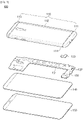
- FIG. 1 illustrates an exploded perspective view of an electronic device according to an embodiment of this disclosure.
- an electronic device 100 includes a housing, a connection member 120, a printed circuit board 130, and a display 140.
- the electronic device 100 may be implemented without some of the components illustrated in FIG. 1 or may be implemented to further include one or more components not illustrated in FIG. 1 .
- the order in which the components included in the electronic device 100 are stacked may be different from the stacked order illustrated in FIG. 1 .
- the housing includes a rear housing 110 and a cover glass 150.
- the rear housing 110 may protect the components included in the electronic device 100.
- the printed circuit board 130, the display 140, a battery, and the like may be accommodated within the rear housing 110, and the rear housing 110 may protect the components from an external shock.
- the rear housing 110 may be formed of tempered glass, plastic, and/or metal.
- the rear housing 110 includes a first conductive region 111, a second conductive region 112, or a third conductive region 113.
- the first conductive region 111, the second conductive region 112, or the third conductive region 113 may be physically separated from each other.
- a non-conductive region 114 e.g., plastic
- a non-conductive material may be interposed between the second conductive region 112 and the third conductive region 113.
- the electronic device 100 uses at least a portion of the first conductive region 111 or the third conductive region 113 as a radiator of an antenna. For example, the electronic device 100 transmits/receives a signal in a high band through the first conductive region 111. For another example, the electronic device 100 may transmit/receive a Wi-Fi signal through the third conductive region 113.
- the second conductive region 112 may be a ground region of an antenna.
- the cover glass 150 may transmit light generated by the display 140.
- the user may touch a portion (e.g., a finger) of his/her body on the cover glass 150 to perform a touch (including a contact using an electronic pen).
- the cover glass 150 may be formed of tempered glass, reinforced plastics, a flexible polymer material, or the like.
- the cover glass 150 may be also referred to as a "glass window"
- connection member 120 is interposed between the rear housing 110 and the printed circuit board 130.
- a first end of the connection member 120 may be electrically connected with the rear housing 110, and a second end of the connection member 120 may be electrically connected with the printed circuit board 130.
- connection member 120 electrically connects the first conductive region 111 and the second conductive region 112.
- the connection member 120 may be attached to the rear housing 110 through an adhesive material.
- the first end of the connection member 120 may be attached to the first conductive region 111, and the second end of the connection member 120 may be attached to the second conductive region 112.
- the first conductive region 111 may be electrically connected with the second conductive region 112 through the connection member 120.
- various electronic parts, elements, or a printed circuit, or the like of the electronic device 100 may be mounted on the printed circuit board (PCB) 130.
- a wireless communication circuit 131 e.g., a communication processor (CP), an application processor (AP), a memory, or the like
- CP communication processor
- AP application processor
- a memory or the like
- the printed circuit board 130 may be referred to as a "main board” or "printed board assembly (PBA)"
- the wireless communication circuit 131 is electrically connected with the first conductive region 111.
- the wireless communication circuit 131 may be connected with a connection element 132 (e.g., a C-clip) positioned at one point on the printed circuit board 130 through a specified wiring (e.g., a flexible printed circuit board (FPCB)).
- the connection element 132 may be in contact with one point of the first conductive region 111.
- the wireless communication circuit 131 may be electrically connected with the first conductive region 111 through the specified wiring and the connection element 132.
- the wireless communication circuit 131 feeds the first conductive region 111, and transmits/receives a signal in a specified frequency band based on an electrical path formed through the first conductive region 111.
- feed or “feeding” may mean an operation in which the wireless communication circuit 131 applies a current to at least a portion of an antenna radiator (e.g., the first conductive region 111 or the third conductive region 113).
- the display 140 may be interposed between the printed circuit board 130 and the cover glass 150.
- the display 140 may be electrically connected with the printed circuit board 130, and may output content (e.g., a text, an image, a video, an icon, a widget, a symbol, or the like).
- content e.g., a text, an image, a video, an icon, a widget, a symbol, or the like.
- the display 140 may receive a touch input (e.g., a touch, a gesture, a hovering, or the like) from the user.
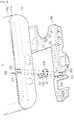
- FIG. 2a illustrates a front surface and a rear surface of a connection member according to an embodiment of this disclosure.
- FIG. 2b illustrates a front surface and a rear surface of a connection member according to an embodiment of this disclosure.
- the connection member 120 includes a non-conductive layer 210, a conductive layer 220, a plurality of metal pads 231, 232, 233, 241, 242, 243, and 244, and at least one circuit element 261 or 262.
- the non-conductive layer 210 may be formed of, for example, plastic.
- the conductive layer 220 may be stacked, for example, on the non-conductive layer 210 and may be formed of a conductive material such as copper (Cu).
- the metal pads 231, 232, and 233 may be positioned adjacent to an edge (e.g., a side) of the connection member 120.
- the first metal pad 231 and the third metal pad 233 may be positioned adjacent to a first end of the connection member 120
- the second metal pad 232 may be positioned adjacent to a second end of the connection member 120.
- the metal pads 241, 242, 243, and 244 connect the at least one circuit element 261 or 262.
- the fifth metal pad 243 and the sixth metal pad 244 may connect the first circuit element 261, and the seventh metal pad 241 and the eighth metal pad 242 may connect the second circuit element 262.
- the at least one circuit element 261 or 262 is interposed between the metal pads 231, 232, and 233.
- the at least one circuit element 261 or 262 is interposed between the first metal pad 231 (or the third metal pad 233) and the second metal pad 232.
- the circuit element 261 or 262 includes a varistor.
- a capacitance of the circuit element 261 or 262 may be, for example, 0.5 pF to 100 pF.
- the at least one circuit element 261 or 262 may be connected with the metal pads 231, 232, and 233 through a specified wiring.
- the first metal pad 231 and the seventh metal pad 241 may be connected through a specified wiring
- the second metal pad 232 and the eighth metal pad 242 may be connected through a specified wiring.
- the second circuit element 262 may be connected with the seventh metal pad 241 and the eighth metal pad 242.
- the first conductive region 111 is connected with the second conductive region 112 through the connection member 120.
- the first conductive region 111 may be connected with the second conductive region 112 through the first metal pad 231, the seventh metal pad 241, the circuit element 262, the eighth metal pad 242, and the second metal pad 232.
- the number of metal pads included in the connection member 120 may be different from the number of metal pads illustrated in FIG. 2a .
- the connection member 120 may include six metal pads 231, 232, 241, 242, 243, and 244 and at least one circuit element 261 or 262.
- the first conductive region 111 may be connected with the second conductive region 112 through the first metal pad 231, the first circuit element 261, the second circuit element 262, and the second metal pad 232.
- an adhesive material 250 may be positioned on a rear surface 120b of the connection member 120.
- the adhesive material 250 may fix the connection member 120 on the rear housing 110.
- the adhesive material 250 may include a conductive tape or the like.
- FIGS. 2a and 2b may be identically applied to components having the same reference numerals/marks as the connection member 120 described with reference to FIGS. 2a and 2b .
- FIG. 3 illustrates a coupling shape between a rear housing, a connection member, and a printed circuit board according to an embodiment of this disclosure.
- connection elements 311, 312, and 313 may be arranged in one region on the printed circuit board 130.
- the connection elements 311, 312, and 313 may be arranged, for example, in a region where the connection member 120 is coupled to the printed circuit board 130.
- the connection elements 311, 312, and 313 may be in contact with the metal pads 231, 232, and 233, for example.
- the first connection element 311 may be in contact with the first metal pad 231
- the second connection element 312 may be in contact with the second metal pad 232
- the third connection element 313 may be in contact with the third metal pad 233.
- connection member 120 may electrically connect the first conductive region 111 and the second conductive region 112.
- a first point 321 on the first conductive region 111 may be in contact with the first metal pad 231, and a second point 322 on the second conductive region 112 may be in contact with the second metal pad 232.
- the third metal pad 233 may be in contact with a third point 323 on the first conductive region 111.
- the first conductive region 111 may be electrically connected with the second conductive region 112 through the first metal pad 231 (and/or the third metal pad 233), the circuit elements 261 and 262, or the second metal pad 232.
- the rear housing 110 is electrically connected with the printed circuit board 130 through the connection member 120.
- the first connection element 311 since the first connection element 311 is in contact with the first metal pad 231, the first point 321 on the first conductive region 111 and the first connection element 311 may be electrically connected.
- the second connection element 312 since the second connection element 312 is in contact with the second metal pad 232, the second point 322 on the second conductive region 112 and the second connection element 312 may be electrically connected.
- FIG. 4a illustrates an electrical path according to an embodiment of this disclosure.
- FIG. 4b illustrates an electrical path according to an embodiment of this disclosure.
- the electronic device 100 may transmit/receive a signal in a first frequency band through a first path 1.
- the electronic device 100 may transmit/receive a signal in a low band and/or a high band through the first path 1.
- the first path 1 may be formed through the connection member 120.
- the electronic device 100 may feed a first point 411 on the printed circuit board 130. Since the first point 411 is connected with a second point 412 on the first conductive region 111 through the connection element 132 (e.g., a C-clip), the fed current may flow from the first point 411 to the second point 412.
- the connection element 132 e.g., a C-clip
- the fed current may flow from the second point 412 to a third point 413 and a fourth point 414.
- the third point 413 and the fourth point 414 may be in contact with the third metal pad 233 and the first metal pad 231, respectively.
- the third metal pad 233 and the first metal pad 231 may be connected with the second metal pad 232 through the at least one circuit element 261 or 262.
- the second metal pad 232 may be electrically connected with a fifth point 415 on the second conductive region 112.
- the fed current may flow from the third point 413 and the fourth point 414 to the second conductive region 112 through the third metal pad 233, the first metal pad 231, the circuit element 261 or 262, the second metal pad 232, and the fifth point 415.
- the electronic device 100 may transmit/receive a signal in a second frequency band through a second path 2.
- the electronic device 100 may transmit/receive a signal in a mid band through the second path 2.
- the second path 2 may be formed through the connection member 120.
- the electronic device 100 may feed a "a" point 421 on the printed circuit board 130. Since the "a" point 421 is connected with a "b" point 422 on the first conductive region 111 through a connection element 431 (e.g., a C-clip), the fed current may flow from the "a" point 421 to the "b" point 422.
- a connection element 431 e.g., a C-clip
- the fed current may flow from the "b” point 422 to a "c" point 423 and a "d” point 424.
- the "c" point 423 and the "d” point 424 may be in contact with the first metal pad 231 and the third metal pad 233, respectively.
- the first metal pad 231 and the third metal pad 233 may be connected with the second metal pad 232 through the at least one circuit element 261 or 262.
- the second metal pad 232 may be electrically connected with an "e” point 425 on the second conductive region 112.
- the fed current may flow from the "c" point 423 and the "d” point 424 to the second conductive region 112 through the first metal pad 231, the third metal pad 233, the at least one circuit element 261 or 262, the second metal pad 232, and the "e” point 425.
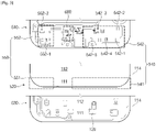
- FIG. 5 illustrates one surface of the printed circuit board 130, and one surface and an opposite surface of the rear housing 110, according to an embodiment of this disclosure.
- One surface 510 of the printed circuit board 130 may mean a surface coupled with the rear housing 110.
- One surface 520 of the rear housing 110 may mean a surface which is opposite to a surface coupled with the printed circuit board 130, and an opposite surface of the rear housing 110 may mean the surface coupled with the printed circuit board 130.
- the electronic device 100 may include the first antenna 540 and the second antenna 550.
- the first antenna 540 may include an "a" region 541 (e.g., a portion of the first conductive region 111), a feeding point 542-1, and a plurality of ground points 542-2, 542-3, 542-4, and 542-5.
- connection elements e.g., a C-clip
- the "a" region 541 may be connected with the feeding point 542-1 and the plurality of ground points 542-2, 542-3, 542-4, and 542-5 through the connection elements.
- the first antenna 540 may be connected with the second conductive region 112 through the connection member 120.
- the second conductive region 112 may be, for example, a ground region of the first antenna 540.
- the first antenna 540 may transmit/receive a signal of the first frequency band through the first path 1.
- the first antenna 540 may transmit/receive a signal in the low band and/or the high band through the first path 1.
- the second antenna 550 may include a "b" region (a portion of the remaining region of the first conductive region 111 other than the "a" region 541), a feeding point 552-1, and a ground point 552-2.
- connection elements e.g., a C-clip
- a "b" region 551 may be connected with the feeding point 552-1 and the ground point 552-2 through the connection elements.
- the second antenna 550 may be connected with the second conductive region 112 through the connection member 120.
- the second conductive region 112 may be, for example, a ground region of the second antenna 550.
- the second antenna 550 may transmit/receive a signal in the second frequency band through the second path 2 illustrated in FIG. 4b .
- the second antenna 550 may transmit/receive a signal in the mid band through the second path 2.
- the first conductive region 111 and the second conductive region 112 are electrically connected through the connection member 120 in the electronic device 100 including the metal rear housing 110.
- the ground region of the first antenna 540 and the second antenna 550 may be expanded, and thus, the isolation between the first antenna 540 and the second antenna 550 may increase.
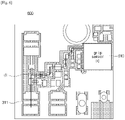
- FIG. 6 illustrates an enlarged view of a partial region of a printed circuit board according to an embodiment of this disclosure.
- a partial region 600 illustrated in FIG. 6 may mean a region of FIG. 5 , at which the printed circuit board 130 and the connection member 120 are coupled.
- a grip sensor circuit 610 is electrically connected with the first conductive region 111 and the second conductive region 112 through a third path 3.
- the third path 3 may mean an electrical path extending from the grip sensor circuit 610 to the first conductive region 111 and the second conductive region 112 through the first connection element 311 and the first metal pad 231.
- the grip sensor circuit 610 may be connected with the first connection element 311, and the first connection element 311 may be in contact with the first metal pad 231 when the connection member 120 is coupled to the printed circuit board 130.
- the first metal pad 231 may be in contact with the first conductive region 111, and may be electrically connected with the second conductive region 112 through the at least one circuit element 261 or 262.
- the grip sensor circuit 610 may be electrically connected with the first conductive region 111 and the second conductive region 112 through the first connection element 311 and the first metal pad 231.
- the grip sensor circuit 610 senses whether a user approaches the electronic device 100 or whether a touch (or a grip) of the user is made, based on a capacitance on the third path 3.
- the capacitance may change when the user approaches the electronic device 100 or when the user touches the electronic device 100.
- the grip sensor circuit 610 may sense whether the user approaches the electronic device 100 or touches the electronic device 100, based on the variation in capacitance.
- the sensing performance of the grip sensor circuit 610 may increase as the capacitance of the circuit element 261 or 262 becomes smaller.
- the capacitance of the second conductive region 112 may be very great.
- the grip sensor circuit 610 may be insensitive to the change (or variation) in capacitance in the case where an electromagnetic effect between the second conductive region 112 and the grip sensor circuit 610 increases.
- the capacitance of the circuit element 261 or 262 is small, the electromagnetic effect between the grip sensor circuit 610 and the second conductive region 112 may decrease, and thus, the grip sensor circuit 610 may sensitively sense the change (or variation) in capacitance.
- the performance of a grip sensor may be improved by inserting the connection member 120 in the electronic device 100 including the metal rear housing 110.
- FIG. 7a illustrates a coupling shape of a printed circuit board and a rear housing according to an embodiment of this disclosure.
- FIG. 7b illustrates an enlarged view of a partial region of a printed circuit board according to an embodiment of this disclosure.
- FIG. 7b is an enlarged view of a partial region 730 illustrated in FIG. 7a .
- An electronic device 700 illustrated in FIG. 7a indicates an electronic device in which, instead of the connection member 120 of the electronic device 100 described with reference to FIGS. 1 to 6 , connection elements 711 and 712 and a circuit element 713 are positioned on the printed circuit board 130.
- the electronic device 700 includes the plurality of connection elements 711 and 712 (e.g., a C-clip) and the at least one circuit element comprising a varistor (713) which are positioned on the printed circuit board 130.
- a position where the plurality of connection elements 711 and 712 and the varistor 713 are positioned may correspond to a position where the connection member 120 is coupled on the printed circuit board 130 in FIG. 3 .
- the first conductive region 111 and the second conductive region 112 are electrically connected through the plurality of connection elements 711 and 712 and the at least one circuit element 713.
- the first connection element 711 may be in contact with one point 721 of the first conductive region 111
- the second connection element 712 may be in contact with one point 722 of the second conductive region 112.
- the circuit element 713 is interposed between the first connection element 711 and the second connection element 712, and may be connected with the first connection element 711 and the second connection element 712 through a specified wiring.
- the first conductive region 111 is connected with the second conductive region 112 through the first connection element 711, the circuit element 713, and the second connection element 712.
- a first antenna 740 transmits/receives a signal in the first frequency band (e.g., the low band and/or the high band).
- the wireless communication circuit 131 feeds a first feeding point 761.
- the fed current may flow to the second conductive region 112 through the first conductive region 111, the first connection element 711, the circuit element 713, and the second connection element 712.
- the first antenna 740 may transmit/receive a signal in the first frequency band based on a path through which the fed current flows.
- the description given with regard to the first antenna 540 may also be applied to the first antenna 740 (illustrated in FIG. 7a ).
- a second antenna 750 may transmit/receive a signal in the second frequency band (e.g., the mid band).
- the wireless communication circuit 131 may feed a second feeding point 762.
- the fed current may flow to the second conductive region 112 through the first conductive region 111, the first connection element 711, the circuit element 713, and the second connection element 712.
- the second antenna 750 may transmit/receive a signal in the second frequency band based on a path through which the fed current flows.
- the description given with regard to the second antenna 550 may also be applied to the second antenna 750 (illustrated in FIG. 7a ).
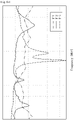
- FIG. 8a illustrates an isolation of antennas and a reflection coefficient of each antenna, according to an embodiment of this disclosure.
- FIG. 8b illustrates an isolation of antennas and a reflection coefficient of each antenna, according to an embodiment of this disclosure.
- FIG. 8c illustrates an isolation of antennas and a reflection coefficient of each antenna, according to an embodiment of this disclosure.
- FIG. 8d illustrates an isolation of antennas and a reflection coefficient of each antenna, according to an embodiment of this disclosure.
- a graph 811 represents an isolation of the first antenna 540 and the second antenna 550 in the electronic device 100 illustrated in FIG. 1
- a graph 812 represents a reflection coefficient of the first antenna 540
- a graph 813 represents a reflection coefficient of the second antenna 550.
- a graph 821 represents an isolation of the first antenna 740 and the second antenna 750 in the electronic device 700 illustrated in FIG. 7a
- a graph 822 represents a reflection coefficient of the first antenna 740
- a graph 823 represents a reflection coefficient of the second antenna 750.
- Graphs 831, 832, and 833 illustrated in FIG. 8c represent an isolation of the antennas 540 and 550 and a reflection coefficient of each of the antenna 540 and the antenna 550 in the case where the first metal pad 231 or the third metal pad 233 is removed from the electronic device 100 illustrated in FIG. 1 (hereinafter referred to as a "first case").
- the graph 831 represents an isolation of the first antenna 540 and the second antenna 550
- a graph 832 represents a reflection coefficient of the first antenna 540
- a graph 833 represents a reflection coefficient of the second antenna 550.
- Graphs 841, 842, and 843 illustrated in FIG. 8d represent an isolation of the antennas 540 and 550 and a reflection coefficient of each of the antenna 540 and the antenna 550 in the case where the connection member 120 is removed from the electronic device 100 illustrated in FIG. 1 (hereinafter referred to as a "second case").
- the graphs 841, 842, and 843 illustrated in FIG. 8d represent an isolation of the antennas 740 and 750 and a reflection coefficient of each of the first antenna 740 and the second antenna 750 in the case where the connection elements 711 and 712 and the circuit element 713 are removed from the electronic device 700 illustrated in FIG. 7a .
- FIGS. 8a to 8d it may be understood from FIGS. 8a to 8d that the electronic device 100 is most excellent in the case of the isolation. It may be understood that an isolation is excellent compared with the first case or the second case even in the case of the electronic device 700 illustrated in FIG. 7a .
- FIGS. 8a to 8d when a ground region of an antenna does not exist or as a ground region of an antenna becomes smaller, a parasitic resonance may increase, and the isolation between the antennas 540 and 550 or 740 and 750 may decrease.
- the electronic device 100 may be understood from a result of comparing reflection coefficients of the antennas 540 and 550 or 740 and 750 that the electronic device 100 is the most excellent.
- the first antenna 540 and the second antenna 550 may have excellent performance in the low band, the mid band, or the high band without a parasitic resonance.
- the performance of the electronic device 700 illustrated in FIG. 7a is somewhat lower than the performance of the electronic device 100, but the electronic device 700 has excellent performance compared with the first case or the second case.
- a parasitic resonance occurring in the second antenna 750 is greater than a parasitic resonance occurring in the second antenna 550 and reflection coefficients of the first antenna 740 and the second antenna 750 are greater than reflection coefficients of the first antenna 540 and the second antenna 550.
- the first case and the second case have very unstable performance compared to the electronic device 100 and the electronic device 700.
- a ground region of an antenna does not exist or as a ground region of an antenna becomes smaller, a parasitic resonance increases, and a reflection coefficient becomes greater.
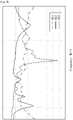
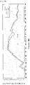
- FIG. 9a illustrates a radiation efficiency of an antenna according to an embodiment of this disclosure.
- FIG. 9b illustrates a reflection coefficient of an antenna according to an embodiment of this disclosure.
- a graph 911 represents a radiation efficiency of the second antenna 550 in the case where the connection member 120 is absent from the electronic device 100
- a graph 912 represents a radiation efficiency of the second antenna 550 according to an embodiment of the present disclosure
- a graph 921 represents a reflection coefficient of the second antenna 550 in the case where the connection member 120 is absent from the electronic device 100
- a graph 922 represents a reflection coefficient of the second antenna 550 according to an embodiment of the present disclosure.
- a radiation efficiency of the second antenna 550 may increase.
- a radiation efficiency of the second antenna 550 may increase in the mid band (e.g., approximately 1900 MHz to approximately 2200 MHz) after inserting the connection member 120.
- the second conductive region 112 of the rear housing 110 may be used as a ground region of the second antenna 550. As such, the radiation efficiency of the antenna 550 may increase.
- a reflection coefficient of the second antenna 550 may decrease.
- a reflection coefficient of the second antenna 550 may decrease in the mid band (e.g., approximately 1900 MHz to approximately 2200 MHz) after inserting the connection member 120.
- the second conductive region 112 of the rear housing 110 may be used as a ground region of the antenna 550. As such, the reflection coefficient of the antenna 550 may decrease.
- the electronic device 100 includes a housing that includes a cover glass 150 through which at least a portion of a display 140 is exposed, and a rear housing 110 coupled with the cover glass 150, wherein the rear housing 110 includes a first conductive region 111, a second conductive region 112 physically spaced from the first conductive region 111, and a non-conductive region (insulating material) 114 interposed between the first conductive region 111 and the second conductive region 112, a printed circuit board 130 that is positioned within the housing, a wireless communication circuit 131 that is positioned on the printed circuit board 130 and is electrically connected with the first conductive region 111, a grip sensor circuit 610 that is positioned on the printed circuit board 130 and is electrically connected with the first conductive region 111, and a connection member 120 that is interposed between the printed circuit board 130 and the rear housing 110 and electrically connects the first conductive region 111 and the second conductive region 112.
- the wireless communication circuit 131 feeds the first conductive region 111 and transmits/receives a signal in a specified frequency band based on a first electrical path formed through the first conductive region 111, the connection member 120, and the second conductive region 112, and the grip sensor circuit 610 senses whether a user approaches the electronic device 100 or whether the user touches the housing, based on a capacitance on a second electrical path connected to the grip sensor circuit 610 from the first conductive region 111 and the second conductive region 112 through the connection member 120.
- connection member 120 includes a first metal pad 231 connected with the first conductive region 111 and a second metal pad 232 connected with the second conductive region 112, and includes a varistor 261 or 262 interposed between the first metal pad 231 and the second metal pad 232.
- the electronic device 100 may further include a first connection element 311 and a second connection element 312 positioned on the printed circuit board 130, and the first metal pad 231 and the second metal pad 232 may be respectively coupled with the first connection element 311 and the second connection element 312.
- the wireless communication circuit 131 transmits/receives the signal of the specified frequency band based on an electrical path formed through the first conductive region 111, the first metal pad 231, the at least one circuit element 261 or 262, the second metal pad 232, and the second conductive region 112.
- connection member 120 may further include a third metal pad 233 connected with the first conductive region 111, and at least one circuit element interposed between the third metal pad 233 and the second metal pad 232.
- the wireless communication circuit 131 may feed a first point 412 on the first conductive region 111 and may transmit/receive a signal of a first frequency band based on an electrical path formed through the first point 412, the first metal pad 231, the at least one circuit element 261 or 262, the second metal pad 232, and the second conductive region 112, and the wireless communication circuit 131 may feed a second point 422 on the first conductive region 111 and transmits/receives a signal of a second frequency band based on an electrical path formed through the second point 422, the first metal pad 231, the at least one circuit element 262 or 262, the second metal pad 232, and the second conductive region 112.
- the first point 411 may be positioned to face the second point 421 with respect to the connection member 120.
- the first frequency band according to an embodiment of the present disclosure may be lower than the second frequency band.
- the grip sensor circuit 610 may sense whether the user approaches the electronic device 100 or whether the user touches the housing, based on a capacitance on a path formed through the first metal pad 231 and the varistor 261 or 262.
- the at least one circuit element 261 or 262 corresponds to a varistor, and a capacitance of the at least one circuit element 261 or 262 may be smaller than a capacitance of the second conductive region 112.
- An adhesive material 250 for attaching the connection member 120 to the housing may be positioned on one surface of the connection member 120.
- the rear housing 110 may further include a third conductive region 113 that is physically connected with the second conductive region 112.
- the specified frequency band may correspond to a first frequency band, and the wireless communication circuit 131 may feed the third conductive region 113 and may transmit/receive a signal of a second frequency band based on an electrical path formed through the third conductive region 113.
- At least a portion of the rear housing 110 may be formed of a conductive material.
- the electronic device 100 includes a housing that includes a cover glass 150 through which at least a portion of a display 140 is exposed, and a rear housing 110 coupled with the cover glass 150, wherein the rear housing 110 includes a first conductive region 111, a second conductive region 112 physically spaced from the first conductive region 111, and a non-conductive region (insulating material) 114 interposed between the first conductive region 111 and the second conductive region 112, a printed circuit board 130 that is positioned within the housing, a wireless communication circuit 131 that is positioned on the printed circuit board 130 and is electrically connected with the first conductive region 111, a grip sensor circuit 610 that is positioned on the printed circuit board 130 and is electrically connected with the first conductive region 111, and a plurality of connection elements 711 and 712 that are positioned on the printed circuit board on a path electrically connecting the first conductive region 111 and the second conductive region 112.
- the wireless communication circuit 131 feeds the first conductive region 111, and transmits/receives a signal in a specified frequency band based on an electrical path formed through the first conductive region 111, the plurality of connection elements 711 and 712, and the second conductive region 112, and the grip sensor circuit 610 senses whether a user approaches the electronic device 100 or whether the user touches the housing, based on a capacitance on an electrical path connected to the grip sensor circuit 610 from the first conductive region 111 and the second conductive region 112 through the plurality of connection elements 711 and 712.
- connection elements 711 and 712 include a first metal clip 711 that is positioned at a first point on the printed circuit board 130, a second metal clip 712 that is positioned at a second point on the printed circuit board 130, and a varistor 713 that is interposed between the first metal clip 711 and the second metal clip 712.
- the first point may correspond to one point on the printed circuit board 130, which corresponds to the first conductive region 111
- the second point may correspond to one point on the printed circuit board 130, which corresponds to the second conductive region 112.
- the wireless communication circuit 131 transmits/receives the signal of the specified frequency band based on an electrical path formed through the first conductive region 111, the first metal clip 711, the circuit element 713, the second metal clip 712, and the second conductive region 112.
- the grip sensor circuit 610 may sense whether the user approaches the electronic device 100 or whether the user touches the housing, based on a capacitance on an electrical path formed through the first metal clip 711 and the varistor 713.
- At least a portion of the first conductive region 111 and at least a portion of the second conductive region 112, according to an embodiment of the present disclosure, may include a conductive material.
- the electronic device 100 may include a housing that includes a cover glass 150 and a rear housing 110 facing the cover glass 150, wherein the rear housing 110 includes a first conductive region 111 including a first edge, a second conductive region 112 including a second edge adjacent to the first edge, and a first non-conductive region 114 electrically separating the first conductive region 111 and the second conductive region 112, and wherein the first non-conductive region 114 extends from the first edge to the second edge so as to contact the first and second edges and is interposed between the first edge and the second edge, a display 140 that is interposed between the cover glass 150 and the rear housing 110 and is exposed through the cover glass 150, a printed circuit board 130 that is interposed between the cover glass 150 and the rear housing 110, a wireless communication circuit 131 that is mounted on the printed circuit board 130 and is electrically connected with a first point of the first conductive region 111, and an connection member 120 that includes a first end electrically connected with a second point of the first conductive
- the circuit element 261 or 262 includes a varistor.
- connection member 120 further includes a structure including a first metal pad 231 being in contact with the second point of the first conductive region 111, and a second metal pad 232 being in contact with the one point of the second conductive region 112.
- the at least one circuit element 261 or 262 electrically connects the first metal pad 231 and the second metal pad 232.
- the structure according to an embodiment of the present disclosure may further include a third metal pad 233 being in contact with a third point of the first conductive region 111, and a distance between the third metal pad 233 and the first metal pad 231 may be shorter than a distance between the second metal pad 232 and the first metal pad 231.
- the structure according to an embodiment of the present disclosure may be mounted on the printed circuit board 130.
- the electronic device 100 may further include a capacitive grip sensor circuit 610 electrically connected with the first conductive region 111.
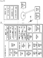
- FIG. 10 illustrates a block diagram of an electronic device in a network environment according to an embodiment of this disclosure.
- an electronic device 1001 may communicate with an electronic device 1002 through a first network 1098 (e.g., a short-range wireless communication) or may communicate with an electronic device 1004 or a server 1008 through a second network 1099 (e.g., a long-distance wireless communication) in a network environment 1000.
- the electronic device 1001 may communicate with the electronic device 1004 through the server 1008.
- the electronic device 1001 may include a processor 1020, a memory 1030, an input device 1050, a sound output device 1055, a display device 1060, an audio module 1070, a sensor module 1076, an interface 1077, a haptic module 1079, a camera module 1080, a power management module 1088, a battery 1089, a communication module 1090, a subscriber identification module 1096, and an antenna module 1097.
- at least one e.g., the display device 1060 or the camera module 1080
- components of the electronic device 1001 may be omitted or other components may be added to the electronic device 1001.
- some components may be integrated and implemented as in the case of the sensor module 1076 (e.g., a fingerprint sensor, an iris sensor, or an illuminance sensor) embedded in the display device 1060 (e.g., a display).
- the sensor module 1076 e.g., a fingerprint sensor, an iris sensor, or an illuminance sensor
- the display device 1060 e.g., a display
- the processor 1020 may operate, for example, software (e.g., a program 1040) to control at least one of other components (e.g., a hardware or software component) of the electronic device 1001 connected to the processor 1020 and may process and compute a variety of data.
- the processor 1020 may load a command set or data, which is received from other components (e.g., the sensor module 1076 or the communication module 1090), into a volatile memory 1032, may process the loaded command or data, and may store result data into a nonvolatile memory 1034.
- the processor 1020 may include a main processor 1021 (e.g., a central processing unit or an application processor) and an coprocessor 1023 (e.g., a graphic processing device, an image signal processor, a sensor hub processor, or a communication processor), which operates independently from the main processor 1021, additionally or alternatively uses less power than the main processor 1021, or is specified to a designated function.
- the coprocessor 1023 may operate separately from the main processor 1021 or embedded.
- the coprocessor 1023 may control, for example, at least some of functions or states associated with at least one component (e.g., the display device 1060, the sensor module 1076, or the communication module 1090) among the components of the electronic device 1001 instead of the main processor 1021 while the main processor 1021 is in an inactive (e.g., sleep) state or together with the main processor 1021 while the main processor 1021 is in an active (e.g., an application execution) state.
- the coprocessor 1023 e.g., the image signal processor or the communication processor
- the memory 1030 may store a variety of data used by at least one component (e.g., the processor 1020 or the sensor module 1076) of the electronic device 1001, for example, software (e.g., the program 1040) and input data or output data with respect to commands associated with the software.
- the memory 1030 may include the volatile memory 1032 or the nonvolatile memory 1034.
- the program 1040 may be stored in the memory 1030 as software and may include, for example, an operating system 1042, a middleware 1044, or an application 1046.
- the input device 1050 may be a device for receiving a command or data, which is used for a component (e.g., the processor 1020) of the electronic device 1001, from an outside (e.g., a user) of the electronic device 1001 and may include, for example, a microphone, a mouse, or a keyboard.
- a component e.g., the processor 1020
- an outside e.g., a user
- a keyboard e.g., a keyboard
- the sound output device 1055 may be a device for outputting a sound signal to the outside of the electronic device 1001 and may include, for example, a speaker used for general purposes, such as multimedia play or recordings play, and a receiver used only for receiving calls. According to an embodiment, the receiver and the speaker may be either integrally or separately implemented.
- the display device 1060 may be a device for visually presenting information to the user and may include, for example, a display, a hologram device, or a projector and a control circuit for controlling a corresponding device. According to an embodiment, the display device 1060 may include a touch circuitry or a pressure sensor for measuring an intensity of pressure on the touch.
- the audio module 1070 may convert a sound and an electrical signal in dual directions. According to an embodiment, the audio module 1070 may obtain the sound through the input device 1050 or may output the sound through an external electronic device (e.g., the electronic device 1002 (e.g., a speaker or a headphone)) wired or wirelessly connected to the sound output device 1055 or the electronic device 1001.
- an external electronic device e.g., the electronic device 1002 (e.g., a speaker or a headphone)
- the sensor module 1076 may generate an electrical signal or a data value corresponding to an operating state (e.g., power or temperature) inside or an environmental state outside the electronic device 1001.
- the sensor module 1076 may include, for example, a gesture sensor, a gyro sensor, a barometric pressure sensor, a magnetic sensor, an acceleration sensor, a grip sensor, a proximity sensor, a color sensor, an infrared sensor, a biometric sensor, a temperature sensor, a humidity sensor, or an illuminance sensor.
- the interface 1077 may support a designated protocol wired or wirelessly connected to the external electronic device (e.g., the electronic device 1002).
- the interface 1077 may include, for example, an HDMI (high-definition multimedia interface), a USB (universal serial bus) interface, an SD card interface, or an audio interface.
- a connection terminal 1078 may include a connector that physically connects the electronic device 1001 to the external electronic device (e.g., the electronic device 1002), for example, an HDMI connector, a USB connector, an SD card connector, or an audio connector (e.g., a headphone connector).
- the external electronic device e.g., the electronic device 1002
- an HDMI connector e.g., a USB connector
- SD card connector e.g., an SD card connector
- an audio connector e.g., a headphone connector
- the haptic module 1079 may convert an electrical signal to a mechanical stimulation (e.g., vibration or movement) or an electrical stimulation perceived by the user through tactile or kinesthetic sensations.
- the haptic module 1079 may include, for example, a motor, a piezoelectric element, or an electric stimulator.
- the camera module 1080 may shoot a still image or a video image.
- the camera module 1080 may include, for example, at least one lens, an image sensor, an image signal processor, or a flash.
- the power management module 1088 may be a module for managing power supplied to the electronic device 1001 and may serve as at least a part of a power management integrated circuit (PMIC).
- PMIC power management integrated circuit
- the battery 1089 may be a device for supplying power to at least one component of the electronic device 1001 and may include, for example, a non-rechargeable (primary) battery, a rechargeable (secondary) battery, or a fuel cell.
- the communication module 1090 may establish a wired or wireless communication channel between the electronic device 1001 and the external electronic device (e.g., the electronic device 1002, the electronic device 1004, or the server 1008) and support communication execution through the established communication channel.
- the communication module 1090 may include at least one communication processor operating independently from the processor 1020 (e.g., the application processor) and supporting the wired communication or the wireless communication.
- the communication module 1090 may include a wireless communication module 1092 (e.g., a cellular communication module, a short-range wireless communication module, or a GNSS (global navigation satellite system) communication module) or a wired communication module 1094 (e.g., an LAN (local area network) communication module or a power line communication module) and may communicate with the external electronic device using a corresponding communication module among them through the first network 1098 (e.g., the short-range communication network such as a Bluetooth, a WiFi direct, or an infrared data association (IrDA)) or the second network 1099 (e.g., the long-distance wireless communication network such as a cellular network, an internet, or a computer network (e.g., LAN or WAN)).
- the above-mentioned various communication modules 1090 may be implemented into one chip or into separate chips, respectively.
- the wireless communication module 1092 may identify and authenticate the electronic device 1001 using user information stored in the subscriber identification module 1096 in the communication network.
- the antenna module 1097 may include one or more antennas to transmit or receive the signal or power to or from an external source.
- the communication module 1090 e.g., the wireless communication module 1092
- Some components among the components may be connected to each other through a communication method (e.g., a bus, a general purpose input/output (GPIO)), an SPI (serial peripheral interface), or an MIPI (mobile industry processor interface)) used between peripheral devices to exchange signals (e.g., a command or data) with each other.
- a communication method e.g., a bus, a general purpose input/output (GPIO)), an SPI (serial peripheral interface), or an MIPI (mobile industry processor interface) used between peripheral devices to exchange signals (e.g., a command or data) with each other.
- GPIO general purpose input/output
- SPI serial peripheral interface
- MIPI mobile industry processor interface
- the command or data may be transmitted or received between the electronic device 1001 and the external electronic device 1004 through the server 1008 connected to the second network 1099.
- Each of the electronic devices 1002 and 1004 may be the same or different types as or from the electronic device 1001.
- all or some of the operations performed by the electronic device 1001 may be performed by another electronic device or a plurality of external electronic devices.
- the electronic device 1001 may request the external electronic device to perform at least some of the functions related to the functions or services, in addition to or instead of performing the functions or services by itself.
- the external electronic device receiving the request may carry out the requested function or the additional function and transmit the result to the electronic device 1001.
- the electronic device 1001 may provide the requested functions or services based on the received result as is or after additionally processing the received result.
- a cloud computing, distributed computing, or client-server computing technology may be used.
- FIG. 11 illustrates a block diagram of a wireless communication module, a power management module, and an antenna module of an electronic device, according to an embodiment of this disclosure.
- the wireless communication module 1092 may include an MST communication module 1110 or an NFC communication module 1130, and the power management module 1088 may include a wireless charging module 1150.
- an antenna module 1197 may separately include a plurality of antennas including an MST antenna 1197-1 connected with the MST communication module 1110, an NFC antenna 1197-3 connected with the NFC communication module 1130, and a wireless charging antenna 1197-5 connected with the wireless charging module 1150.
- the MST communication module 1110 may receive a signal (e.g., a signal including control information or payment information) from the processor 1020, may generate a magnetic signal corresponding to the received signal through the MST antenna 1197-1, and may transmit the generated magnetic signal to the external electronic device 1002 (e.g., a POS device).
- the MST communication module 1110 may include a switching module (not illustrated) including one or more switches connected with the MST antenna 1197-1, and may control the switching module to change a direction of a voltage or a current to be supplied to the MST antenna 1197-1.
- a direction of a magnetic signal (e.g., a magnetic field) to be transmitted to the external electronic device 1002 through the short-range wireless communication 1098 may be changed, for example, by transmitting the magnetic signal through the MST antenna 1197-1.
- the magnetic signal transmitted with the direction changed may cause a form and an effect which are similar to those of a magnetic field generated while (or when) a magnetic card is swiped by a card reader of the electronic device 1002.
- payment-related information and a control signal received from the electronic device 1002 in the form of the magnetic signal may be transmitted, for example, to a server (e.g., the server 1008) through the network 1099.
- the NFC communication module 1130 may obtain a signal (e.g., control information or payment information) from the processor 1020, and may transmit the obtained signal to the external electronic device 1002 through the NFC antenna 1197-3. According to an embodiment, the NFC communication module 1130 may receive a signal (e.g., a signal including control information or payment information) transmitted from the external electronic device 1002 through the NFC antenna 1197-3.
- a signal e.g., control information or payment information
- the wireless charging module 1150 may wirelessly transmit a power to the external electronic device 1002 (e.g., a mobile phone or a wearable device) through the wireless charging antenna 1197-5, or may wirelessly receive a power from the external electronic device 1002 (e.g., a wireless charging device).
- the wireless charging module 1150 may support various wireless charging manners, for example, including a magnetic resonance manner or a magnetic induction manner.
- some of the MST antenna 1197-1, the NFC antenna 1197-3, or the wireless charging antenna 1197-5 may mutually share at least a portion of a radiation unit (or radiator).
- a radiation unit of the MST antenna 1197-1 may be used as a radiation unit of the NFC antenna 1197-3 or the wireless charging antenna 1197-5, and vice versa.
- the antenna module 1197 may include a switching circuit (not illustrated) for selectively connecting or separating (e.g., opening) at least some of the antennas 1197-1, 1197-3, and 1197-3 under control of the wireless communication module 1092 (e.g., the MST communication module 1110 or the NFC communication module 1130) or the power management module 1088 (e.g., the wireless charging module 1150).
- the wireless communication module 1092 e.g., the MST communication module 1110 or the NFC communication module 1130
- the power management module 1088 e.g., the wireless charging module 1150.
- the NFC communication module 1130 or the wireless charging module 1150 may control the switching circuit such that the at least a partial region of the radiation unit shared by the NFC antenna 1197-3 and the wireless charging antenna 1197-5 is temporarily separated from the NFC antenna 1197-3 and is connected only with the wireless charging antenna 1197-5.
- At least a part of functions of the MST communication module 1110, the NFC communication module 1130, or the Wireless charging module 1150 may be controlled by an external processor (e.g., the processor 1020).
- specified functions (e.g., a payment function) of the MST communication module 1110 or the NFC communication module 1130 may be performed in a trusted execution environment (TEE).
- TEE trusted execution environment
- the trusted execution environment may be, for example, an execution environment in which at least a portion of a specified region of the memory 1030 is assigned to perform a function (e.g., a financial transaction or a private information related function) needing a relatively high level of security and an access to the specified region is separately and restrictively allowed, for example, depending on an access subject or an application to be executed.
- a function e.g., a financial transaction or a private information related function
- the electronic device may be various types of devices.
- the electronic device may include, for example, at least one of a portable communication device (e.g., a smartphone), a computer device, a portable multimedia device, a mobile medical appliance, a camera, a wearable device, or a home appliance.
- a portable communication device e.g., a smartphone
- a computer device e.g
- a first”, “a second”, “the first”, or “the second”, used in herein may refer to various components regardless of the order and/or the importance, but do not limit the corresponding components.
- the above expressions are used merely for the purpose of distinguishing a component from the other components. It should be understood that when a component (e.g., a first component) is referred to as being (operatively or communicatively) "connected,” or “coupled,” to another component (e.g., a second component), it may be directly connected or coupled directly to the other component or any other component (e.g., a third component) may be interposed between them.
- module used herein may represent, for example, a unit including one or more combinations of hardware, software and firmware.
- module may be interchangeably used with the terms “logic”, “logical block”, “part” and “circuit”.
- the “module” may be a minimum unit of an integrated part or may be a part thereof.
- the “module” may be a minimum unit for performing one or more functions or a part thereof.
- the “module” may include an application-specific integrated circuit (ASIC).
- ASIC application-specific integrated circuit
- Various embodiments of the present disclosure may be implemented by software (e.g., the program 1040) including an instruction stored in a machine-readable storage media (e.g., an internal memory 1036 or an external memory 1038) readable by a machine (e.g., a computer).
- the machine may be a device that calls the instruction from the machine-readable storage media and operates depending on the called instruction and may include the electronic device (e.g., the electronic device 1001).
- the processor e.g., the processor 1020
- the processor may perform a function corresponding to the instruction directly or using other components under the control of the processor.
- the instruction may include a code generated or executed by a compiler or an interpreter.
- the machine-readable storage media may be provided in the form of non-transitory storage media.
- non-transitory is a limitation of the medium itself (i.e., tangible, not a signal) as opposed to a limitation on data storage persistency.
- the method according to various embodiments disclosed in the present disclosure may be provided as a part of a computer program product.
- the computer program product may be traded between a seller and a buyer as a product.
- the computer program product may be distributed in the form of machine-readable storage medium (e.g., a compact disc read only memory (CD-ROM)) or may be distributed only through an application store (e.g., a PLAY STORE).
- an application store e.g., a PLAY STORE
- at least a portion of the computer program product may be temporarily stored or generated in a storage medium such as a memory of a manufacturer's server, an application store's server, or a relay server.
Landscapes
- Engineering & Computer Science (AREA)
- Computer Networks & Wireless Communication (AREA)
- Signal Processing (AREA)
- General Engineering & Computer Science (AREA)
- Theoretical Computer Science (AREA)
- Human Computer Interaction (AREA)
- Physics & Mathematics (AREA)
- General Physics & Mathematics (AREA)
- Support Of Aerials (AREA)
- Telephone Set Structure (AREA)
Claims (14)
- Elektronische Vorrichtung (100), welche Folgendes umfasst:ein Gehäuse, wobei das Gehäuse Folgendes enthält:ein Deckglas (150), das mindestens einen Teil eines Displays (140) freilegt; undein hinteres Gehäuse (110), das mit dem Deckglas gekoppelt ist, wobei das hintere Gehäuse einen ersten leitfähigen Bereich (111), einen zweiten leitfähigen Bereich (112), der physikalisch von dem ersten leitfähigen Bereich (111) beabstandet ist, und ein Isolationsmaterial enthält, das zwischen dem ersten leitfähigen Bereich (111) und dem zweiten leitfähigen Bereich (112) angeordnet ist;eine Leiterplatte (130), die innerhalb des Gehäuses positioniert ist;einen drahtlosen Kommunikationsschaltkreis (131), der auf der Leiterplatte (130) positioniert ist und mit dem ersten leitfähigen Bereich (111) elektrisch verbunden ist;eine Griffsensorschaltung (610), die auf der Leiterplatte (130) positioniert ist und mit dem ersten leitfähigen Bereich (111) elektrisch verbunden ist; undein Verbindungselement (120), das zwischen der Leiterplatte (130) und dem hinteren Gehäuse (110) angeordnet ist und den ersten leitfähigen Bereich (111) und den zweiten leitfähigen Bereich (112) elektrisch verbindet,wobei der drahtlose Kommunikationsschaltkreis (131) konfiguriert ist zum:Speisen des ersten leitfähigen Bereichs (111); undÜbertragen oder Empfangen eines Signals in einem spezifizierten Frequenzband basierend auf einem ersten elektrischen Pfad, der durch den ersten leitfähigen Bereich (111), das Verbindungselement (120) und den zweiten leitfähigen Bereich (112) gebildet wird, undwobei die Griffsensorschaltung (610) konfiguriert ist, um zu erfassen, ob sich ein Benutzer der elektronischen Vorrichtung (100) nähert oder ob der Benutzer das Gehäuse berührt, basierend auf einer Kapazität auf einem zweiten elektrischen Pfad, der mit der Griffsensorschaltung (610) von dem ersten leitfähigen Bereich (111) und dem zweiten leitfähigen Bereich (112) durch das Verbindungselement (120) verbunden wird,wobei das Verbindungselement (120) ein erstes Metallpad (231), das mit dem ersten leitfähigen Bereich (111) verbunden ist, und ein zweites Metallpad (232) enthält, das mit dem zweiten leitfähigen Bereich (112) verbunden ist, und gekennzeichnet dadurch, dass das Verbindungselement einen Varistor (261, 262) enthält, der zwischen dem ersten Metallpad (231) und dem zweiten Metallpad (232) angeordnet ist.
- Elektronische Vorrichtung (100) nach Anspruch 1, welche ferner Folgendes umfasst:
ein erstes Verbindungselement (311) und ein zweites Verbindungselement (312), die auf der Leiterplatte (130) positioniert sind, wobei das erste Metallpad (231) und das zweite Metallpad (232) jeweils mit dem ersten Verbindungselement und dem zweiten Verbindungselement gekoppelt sind. - Elektronische Vorrichtung (100) nach Anspruch 1, wobei der drahtlose Kommunikationsschaltkreis (131) konfiguriert ist, um das Signal des spezifizierten Frequenzbandes basierend auf einem elektrischen Pfad zu übertragen oder zu empfangen, der durch den ersten leitfähigen Bereich, das erste Metallpad, den Varistor, das zweite Metallpad und den zweiten leitfähigen Bereich gebildet wird.
- Elektronische Vorrichtung (100) nach Anspruch 1, wobei das Verbindungselement (120) ferner Folgendes enthält:ein drittes Metallpad (233), das mit dem ersten leitfähigen Bereich (111) verbunden ist; undein Schaltkreiselement, das zwischen dem dritten Metallpad (233) und dem zweiten Metallpad (232) angeordnet ist.
- Elektronische Vorrichtung (100) nach Anspruch 1, wobei der drahtlose Kommunikationsschaltkreis (131) konfiguriert ist, um einen ersten Punkt (411) auf dem ersten leitfähigen Bereich (111) zu speisen und ein Signal eines ersten Frequenzbandes basierend auf einem elektrischen Pfad zu übertragen oder zu empfangen, der durch den ersten Punkt (411), das erste Metallpad (231), den Varistor, das zweite Metallpad (232) und den zweiten leitfähigen Bereich (112) gebildet wird, und
wobei der drahtlose Kommunikationsschaltkreis (131) konfiguriert ist, um einen zweiten Punkt (421) auf dem ersten leitfähigen Bereich (111) zu speisen und ein Signal eines zweiten Frequenzbandes basierend auf einem elektrischen Pfad zu übertragen oder zu empfangen, der durch den zweiten Punkt (421), das erste Metallpad (231), den Varistor, das zweite Metallpad (232) und den zweiten leitfähigen Bereich (112) gebildet wird. - Elektronische Vorrichtung (100) nach Anspruch 5, wobei der erste Punkt (411) und der zweite (421) Punkt an gegenüberliegenden Enden des Verbindungselements (120) positioniert sind.
- Elektronische Vorrichtung (100) nach Anspruch 5, wobei das erste Frequenzband niedriger als das zweite Frequenzband ist.
- Elektronische Vorrichtung (100) nach Anspruch 1, wobei die Griffsensorschaltung (610) konfiguriert ist, um zu erfassen, ob sich der Benutzer der elektronischen Vorrichtung (100) nähert oder ob der Benutzer das Gehäuse berührt, basierend auf einer Kapazität auf einem Pfad, der durch das erste Metallpad (231) und den Varistor gebildet wird.
- Elektronische Vorrichtung (100) nach Anspruch 1, wobei eine Kapazität des Varistors kleiner als eine Kapazität des zweiten leitfähigen Bereichs (112) ist.
- Elektronische Vorrichtung (100) nach Anspruch 1, welche ferner ein Klebematerial zum Befestigen des Verbindungselements an dem Gehäuse umfasst, wobei das Klebematerial auf einer Oberfläche des Verbindungselements positioniert ist.
- Elektronische Vorrichtung (100) nach Anspruch 1, wobei das hintere Gehäuse ferner Folgendes enthält:
einen dritten leitfähigen Bereich, der mit dem zweiten leitfähigen Bereich physikalisch verbunden ist. - Elektronische Vorrichtung (100) nach Anspruch 11, wobei das spezifizierte Frequenzband einem ersten Frequenzband entspricht, und
wobei der drahtlose Kommunikationsschaltkreis (131) konfiguriert ist, um den dritten leitfähigen Bereich zu speisen und ein Signal eines zweiten Frequenzbandes basierend auf einem elektrischen Pfad zu übertragen oder zu empfangen, der durch den dritten leitfähigen Bereich gebildet wird. - Elektronische Vorrichtung (100) nach Anspruch 1, wobei mindestens ein Teil des hinteren Gehäuses aus einem leitfähigen Material gebildet wird.
- Elektronische Vorrichtung (100), welche Folgendes umfasst: ein Gehäuse, wobei das Gehäuse Folgendes enthält: ein Deckglas, das mindestens einen Teil eines Displays freilegt; und ein hinteres Gehäuse, das mit dem Deckglas gekoppelt ist, wobei das hintere Gehäuse einen ersten leitfähigen Bereich, einen zweiten leitfähigen Bereich, der physikalisch von dem ersten leitfähigen Bereich beabstandet ist, und ein Isolationsmaterial enthält, das zwischen dem ersten leitfähigen Bereich und dem zweiten leitfähigen Bereich angeordnet ist; eine Leiterplatte, die innerhalb des Gehäuses positioniert ist;einen drahtlosen Kommunikationsschaltkreis, der auf der Leiterplatte positioniert ist und mit dem ersten leitfähigen Bereich elektrisch verbunden ist; eine Griffsensorschaltung, die auf der Leiterplatte positioniert ist und mit dem ersten leitfähigen Bereich elektrisch verbunden ist; undgekennzeichnet dadurch, dass die elektronische Vorrichtung ferner eine Vielzahl von Verbindungselementen (711, 712) umfasst, die ein erstes Verbindungselement (711) und ein zweites Verbindungselement (712) umfassen, die auf der Leiterplatte auf einem Pfad positioniert sind, der den ersten leitfähigen Bereich und den zweiten leitfähigen Bereich elektrisch verbindet, einen Varistor (713), der auf der Leiterplatte positioniert ist, wobei der Varistor zwischen dem ersten Verbindungselement und dem zweiten Verbindungselement angeordnet ist und mit dem ersten Verbindungselement und dem zweiten Verbindungselement durch eine spezifizierte Verdrahtung verbunden ist, so dass der erste leitfähige Bereich mit dem zweiten leitfähigen Bereich durch das erste Verbindungselement, den Varistor und das zweite Verbindungselement verbunden ist,wobei der drahtlose Kommunikationsschaltkreis konfiguriert ist zum: Speisen des ersten leitfähigen Bereichs; und Übertragen oder Empfangen eines Signals in einem spezifizierten Frequenzband basierend auf einem elektrischen Pfad, der durch den ersten leitfähigen Bereich, die Vielzahl von Verbindungselementen und den zweiten leitfähigen Bereich gebildet wird, und wobei die Griffsensorschaltung konfiguriert ist, um zu erfassen, ob sich ein Benutzer der elektronischen Vorrichtung nähert oder ob der Benutzer das Gehäuse berührt, basierend auf einer Kapazität auf einem elektrischen Pfad, der mit der Griffsensorschaltung von dem ersten leitfähigen Bereich und dem zweiten leitfähigen Bereich durch die Vielzahl von Verbindungselementen verbunden ist.
Applications Claiming Priority (2)
| Application Number | Priority Date | Filing Date | Title |
|---|---|---|---|
| KR1020170110505A KR102376211B1 (ko) | 2017-08-30 | 2017-08-30 | 그립 센서 및 안테나를 포함하는 전자 장치 |
| PCT/KR2018/010021 WO2019045461A1 (en) | 2017-08-30 | 2018-08-30 | ELECTRONIC DEVICE COMPRISING A GRIP SENSOR AND ANTENNA |
Publications (3)
| Publication Number | Publication Date |
|---|---|
| EP3656112A1 EP3656112A1 (de) | 2020-05-27 |
| EP3656112A4 EP3656112A4 (de) | 2020-07-08 |
| EP3656112B1 true EP3656112B1 (de) | 2022-04-27 |
Family
ID=65437696
Family Applications (1)
| Application Number | Title | Priority Date | Filing Date |
|---|---|---|---|
| EP18849891.9A Active EP3656112B1 (de) | 2017-08-30 | 2018-08-30 | Elektronische vorrichtung mit griffsensor und antenne |
Country Status (4)
| Country | Link |
|---|---|
| US (2) | US10559873B2 (de) |
| EP (1) | EP3656112B1 (de) |
| KR (1) | KR102376211B1 (de) |
| WO (1) | WO2019045461A1 (de) |
Families Citing this family (17)
| Publication number | Priority date | Publication date | Assignee | Title |
|---|---|---|---|---|
| KR20180122231A (ko) * | 2017-05-02 | 2018-11-12 | 엘지전자 주식회사 | 이동 단말기 |
| KR102426351B1 (ko) * | 2017-09-29 | 2022-07-29 | 삼성전자주식회사 | 그립 센싱을 위한 전자 장치 및 그 동작 방법 |
| US11064625B2 (en) * | 2018-04-26 | 2021-07-13 | Mitsubishi Electric Corporation | Interface circuit, substrate, electronic device, and programmable controller |
| KR102662537B1 (ko) | 2019-05-10 | 2024-05-02 | 삼성전자 주식회사 | 이중 대역 안테나 및 그것을 포함하는 전자 장치 |
| KR102624300B1 (ko) * | 2019-05-23 | 2024-01-15 | 삼성전자주식회사 | 인쇄 회로 기판 및 하우징을 전기적으로 연결시키기 위한 연결 구조를 포함하는 전자 장치 |
| KR20210092611A (ko) * | 2020-01-16 | 2021-07-26 | 삼성전자주식회사 | 안테나 포함하는 전자 장치 |
| US11876279B2 (en) * | 2020-02-25 | 2024-01-16 | Microsoft Technology Licensing, Llc | Hybrid cavity mode antenna |
| KR102756064B1 (ko) * | 2020-03-12 | 2025-01-17 | 삼성전자주식회사 | 안테나 및 그립 센서를 포함하는 전자 장치 |
| US11038556B1 (en) * | 2020-06-25 | 2021-06-15 | Nxp B.V. | Near-field communications device |
| US11108437B1 (en) | 2020-07-02 | 2021-08-31 | Nxp B.V. | Near-field communications device |
| WO2022025594A1 (ko) | 2020-07-27 | 2022-02-03 | 삼성전자 주식회사 | 그립 센서를 포함하는 전자 장치에서 디스플레이의 확장 여부에 따라 전송 전력을 조절하는 장치 및 방법 |
| KR102902132B1 (ko) * | 2020-09-04 | 2025-12-19 | 삼성전자 주식회사 | 커패시턴스 센서를 포함하는 전자 장치 |
| EP4228161B1 (de) | 2021-01-25 | 2026-03-04 | Samsung Electronics Co., Ltd. | Elektronische vorrichtung und verfahren zur steuerung der übertragungsleistung eines kommunikationsmoduls |
| EP4319109A4 (de) | 2021-05-20 | 2024-09-04 | Samsung Electronics Co., Ltd. | Elektronische vorrichtung mit griffsensor |
| KR20230005630A (ko) | 2021-07-01 | 2023-01-10 | 삼성전자주식회사 | 안테나를 포함하는 전자 장치 |
| US12368464B2 (en) | 2022-02-08 | 2025-07-22 | Samsung Electronics Co., Ltd. | Electronic device including grip sensor and antenna |
| WO2025249849A1 (ko) * | 2024-05-29 | 2025-12-04 | 삼성전자 주식회사 | 그립 센서를 포함하는 전자 장치 |
Family Cites Families (12)
| Publication number | Priority date | Publication date | Assignee | Title |
|---|---|---|---|---|
| US8432322B2 (en) | 2009-07-17 | 2013-04-30 | Apple Inc. | Electronic devices with capacitive proximity sensors for proximity-based radio-frequency power control |
| KR101685363B1 (ko) * | 2010-09-27 | 2016-12-12 | 엘지전자 주식회사 | 휴대 단말기 및 그 동작 방법 |
| US8577289B2 (en) | 2011-02-17 | 2013-11-05 | Apple Inc. | Antenna with integrated proximity sensor for proximity-based radio-frequency power control |
| KR102120099B1 (ko) | 2013-02-06 | 2020-06-09 | 엘지전자 주식회사 | 양면 터치 인식 가능한 디지털 디바이스 및 제어 방법 |
| US20150205400A1 (en) * | 2014-01-21 | 2015-07-23 | Microsoft Corporation | Grip Detection |
| US10122081B2 (en) * | 2014-03-13 | 2018-11-06 | Google Technology Holdings LLC | Hand grip sensor for external chassis antenna |
| KR102176368B1 (ko) * | 2015-01-05 | 2020-11-09 | 엘지전자 주식회사 | 안테나 모듈 및 이를 구비하는 이동 단말기 |
| CN105024162B (zh) * | 2015-07-08 | 2018-06-26 | 深圳市信维通信股份有限公司 | 一种带有金属后壳的nfc天线 |
| CN104993216A (zh) | 2015-07-17 | 2015-10-21 | 苏州纳安特通信科技有限公司 | 用于金属背盖手机的nfc天线结构 |
| US10056695B2 (en) | 2015-07-28 | 2018-08-21 | Apple Inc. | Electronic device antenna with switchable return paths |
| KR102408870B1 (ko) * | 2015-08-13 | 2022-06-15 | 삼성전자주식회사 | 안테나 장치 및 그것을 포함하는 전자 장치 |
| KR102465926B1 (ko) * | 2015-11-25 | 2022-11-14 | 삼성전자주식회사 | 안테나 장치 및 그것을 포함하는 전자 장치 |
-
2017
- 2017-08-30 KR KR1020170110505A patent/KR102376211B1/ko active Active
-
2018
- 2018-08-30 WO PCT/KR2018/010021 patent/WO2019045461A1/en not_active Ceased
- 2018-08-30 US US16/117,739 patent/US10559873B2/en active Active
- 2018-08-30 EP EP18849891.9A patent/EP3656112B1/de active Active
-
2019
- 2019-12-31 US US16/731,784 patent/US10854958B2/en active Active
Also Published As
| Publication number | Publication date |
|---|---|
| US20200136237A1 (en) | 2020-04-30 |
| US10559873B2 (en) | 2020-02-11 |
| KR102376211B1 (ko) | 2022-03-21 |
| EP3656112A4 (de) | 2020-07-08 |
| US20190067801A1 (en) | 2019-02-28 |
| KR20190023995A (ko) | 2019-03-08 |
| EP3656112A1 (de) | 2020-05-27 |
| WO2019045461A1 (en) | 2019-03-07 |
| US10854958B2 (en) | 2020-12-01 |
Similar Documents
| Publication | Publication Date | Title |
|---|---|---|
| US10854958B2 (en) | Electronic device including grip sensor and antenna | |
| US12034466B2 (en) | Antenna and foldable electronic device including the same | |
| US11886238B2 (en) | Foldable electronic device | |
| US20230299460A1 (en) | Antenna and electronic device including the same | |
| EP3794808B1 (de) | Elektronische vorrichtung mit einer an die antenne angrenzenden flexiblen leiterplatte | |
| EP3903377B1 (de) | Elektronische vorrichtung mit erweitertem flexiblen leiterplattenantennenmodul | |
| EP3738296B1 (de) | Elektronische vorrichtung mit metallabdeckung als antennenstrahler | |
| US20210325981A1 (en) | Electronic device and stylus pen charging method using same | |
| CN112567320A (zh) | 包括按钮的电子装置以及用于电子装置中的操作的方法 | |
| US11144156B2 (en) | Electronic device including display and sensor | |
| US11700324B2 (en) | Electronic device having connection path between buck converters | |
| US11271284B2 (en) | Electronic device comprising at least one switch for supplying electricity to loop antenna |
Legal Events
| Date | Code | Title | Description |
|---|---|---|---|
| STAA | Information on the status of an ep patent application or granted ep patent |
Free format text: STATUS: THE INTERNATIONAL PUBLICATION HAS BEEN MADE |
|
| PUAI | Public reference made under article 153(3) epc to a published international application that has entered the european phase |
Free format text: ORIGINAL CODE: 0009012 |
|
| STAA | Information on the status of an ep patent application or granted ep patent |
Free format text: STATUS: REQUEST FOR EXAMINATION WAS MADE |
|
| 17P | Request for examination filed |
Effective date: 20200221 |
|
| AK | Designated contracting states |
Kind code of ref document: A1 Designated state(s): AL AT BE BG CH CY CZ DE DK EE ES FI FR GB GR HR HU IE IS IT LI LT LU LV MC MK MT NL NO PL PT RO RS SE SI SK SM TR |
|
| AX | Request for extension of the european patent |
Extension state: BA ME |
|
| A4 | Supplementary search report drawn up and despatched |
Effective date: 20200609 |
|
| RIC1 | Information provided on ipc code assigned before grant |
Ipc: H04M 1/02 20060101ALI20200604BHEP Ipc: H01Q 5/378 20150101ALI20200604BHEP Ipc: H04M 1/725 20060101ALN20200604BHEP Ipc: H01Q 1/24 20060101AFI20200604BHEP Ipc: H01Q 13/10 20060101ALI20200604BHEP Ipc: H01Q 5/364 20150101ALI20200604BHEP Ipc: H01Q 9/42 20060101ALN20200604BHEP Ipc: H01Q 5/50 20150101ALI20200604BHEP Ipc: H01Q 5/35 20150101ALI20200604BHEP |
|
| DAV | Request for validation of the european patent (deleted) | ||
| DAX | Request for extension of the european patent (deleted) | ||
| REG | Reference to a national code |
Ref country code: DE Ref legal event code: R079 Ref document number: 602018034664 Country of ref document: DE Free format text: PREVIOUS MAIN CLASS: H04M0001020000 Ipc: H01Q0001240000 |
|
| RIC1 | Information provided on ipc code assigned before grant |
Ipc: H04M 1/725 20210101ALN20211027BHEP Ipc: H01Q 9/42 20060101ALN20211027BHEP Ipc: H01Q 5/378 20150101ALI20211027BHEP Ipc: H01Q 5/364 20150101ALI20211027BHEP Ipc: H01Q 5/35 20150101ALI20211027BHEP Ipc: H01Q 13/10 20060101ALI20211027BHEP Ipc: H01Q 5/50 20150101ALI20211027BHEP Ipc: H04M 1/02 20060101ALI20211027BHEP Ipc: H01Q 1/24 20060101AFI20211027BHEP |
|
| GRAP | Despatch of communication of intention to grant a patent |
Free format text: ORIGINAL CODE: EPIDOSNIGR1 |
|
| STAA | Information on the status of an ep patent application or granted ep patent |
Free format text: STATUS: GRANT OF PATENT IS INTENDED |
|
| RIC1 | Information provided on ipc code assigned before grant |
Ipc: H04M 1/725 20210101ALN20211124BHEP Ipc: H01Q 9/42 20060101ALN20211124BHEP Ipc: H01Q 5/378 20150101ALI20211124BHEP Ipc: H01Q 5/364 20150101ALI20211124BHEP Ipc: H01Q 5/35 20150101ALI20211124BHEP Ipc: H01Q 13/10 20060101ALI20211124BHEP Ipc: H01Q 5/50 20150101ALI20211124BHEP Ipc: H04M 1/02 20060101ALI20211124BHEP Ipc: H01Q 1/24 20060101AFI20211124BHEP |
|
| INTG | Intention to grant announced |
Effective date: 20211210 |
|
| RIC1 | Information provided on ipc code assigned before grant |
Ipc: H04M 1/725 20210101ALN20211126BHEP Ipc: H01Q 9/42 20060101ALN20211126BHEP Ipc: H01Q 5/378 20150101ALI20211126BHEP Ipc: H01Q 5/364 20150101ALI20211126BHEP Ipc: H01Q 5/35 20150101ALI20211126BHEP Ipc: H01Q 13/10 20060101ALI20211126BHEP Ipc: H01Q 5/50 20150101ALI20211126BHEP Ipc: H04M 1/02 20060101ALI20211126BHEP Ipc: H01Q 1/24 20060101AFI20211126BHEP |
|
| GRAS | Grant fee paid |
Free format text: ORIGINAL CODE: EPIDOSNIGR3 |
|
| GRAA | (expected) grant |
Free format text: ORIGINAL CODE: 0009210 |
|
| STAA | Information on the status of an ep patent application or granted ep patent |
Free format text: STATUS: THE PATENT HAS BEEN GRANTED |
|
| AK | Designated contracting states |
Kind code of ref document: B1 Designated state(s): AL AT BE BG CH CY CZ DE DK EE ES FI FR GB GR HR HU IE IS IT LI LT LU LV MC MK MT NL NO PL PT RO RS SE SI SK SM TR |
|
| REG | Reference to a national code |
Ref country code: GB Ref legal event code: FG4D |
|
| REG | Reference to a national code |
Ref country code: CH Ref legal event code: EP |
|
| REG | Reference to a national code |
Ref country code: DE Ref legal event code: R096 Ref document number: 602018034664 Country of ref document: DE |
|
| REG | Reference to a national code |
Ref country code: AT Ref legal event code: REF Ref document number: 1487682 Country of ref document: AT Kind code of ref document: T Effective date: 20220515 |
|
| REG | Reference to a national code |
Ref country code: IE Ref legal event code: FG4D |
|
| REG | Reference to a national code |
Ref country code: LT Ref legal event code: MG9D |
|
| REG | Reference to a national code |
Ref country code: NL Ref legal event code: MP Effective date: 20220427 |
|
| REG | Reference to a national code |
Ref country code: AT Ref legal event code: MK05 Ref document number: 1487682 Country of ref document: AT Kind code of ref document: T Effective date: 20220427 |
|
| PG25 | Lapsed in a contracting state [announced via postgrant information from national office to epo] |
Ref country code: NL Free format text: LAPSE BECAUSE OF FAILURE TO SUBMIT A TRANSLATION OF THE DESCRIPTION OR TO PAY THE FEE WITHIN THE PRESCRIBED TIME-LIMIT Effective date: 20220427 |
|
| PG25 | Lapsed in a contracting state [announced via postgrant information from national office to epo] |
Ref country code: SE Free format text: LAPSE BECAUSE OF FAILURE TO SUBMIT A TRANSLATION OF THE DESCRIPTION OR TO PAY THE FEE WITHIN THE PRESCRIBED TIME-LIMIT Effective date: 20220427 Ref country code: PT Free format text: LAPSE BECAUSE OF FAILURE TO SUBMIT A TRANSLATION OF THE DESCRIPTION OR TO PAY THE FEE WITHIN THE PRESCRIBED TIME-LIMIT Effective date: 20220829 Ref country code: NO Free format text: LAPSE BECAUSE OF FAILURE TO SUBMIT A TRANSLATION OF THE DESCRIPTION OR TO PAY THE FEE WITHIN THE PRESCRIBED TIME-LIMIT Effective date: 20220727 Ref country code: LT Free format text: LAPSE BECAUSE OF FAILURE TO SUBMIT A TRANSLATION OF THE DESCRIPTION OR TO PAY THE FEE WITHIN THE PRESCRIBED TIME-LIMIT Effective date: 20220427 Ref country code: HR Free format text: LAPSE BECAUSE OF FAILURE TO SUBMIT A TRANSLATION OF THE DESCRIPTION OR TO PAY THE FEE WITHIN THE PRESCRIBED TIME-LIMIT Effective date: 20220427 Ref country code: GR Free format text: LAPSE BECAUSE OF FAILURE TO SUBMIT A TRANSLATION OF THE DESCRIPTION OR TO PAY THE FEE WITHIN THE PRESCRIBED TIME-LIMIT Effective date: 20220728 Ref country code: FI Free format text: LAPSE BECAUSE OF FAILURE TO SUBMIT A TRANSLATION OF THE DESCRIPTION OR TO PAY THE FEE WITHIN THE PRESCRIBED TIME-LIMIT Effective date: 20220427 Ref country code: ES Free format text: LAPSE BECAUSE OF FAILURE TO SUBMIT A TRANSLATION OF THE DESCRIPTION OR TO PAY THE FEE WITHIN THE PRESCRIBED TIME-LIMIT Effective date: 20220427 Ref country code: BG Free format text: LAPSE BECAUSE OF FAILURE TO SUBMIT A TRANSLATION OF THE DESCRIPTION OR TO PAY THE FEE WITHIN THE PRESCRIBED TIME-LIMIT Effective date: 20220727 Ref country code: AT Free format text: LAPSE BECAUSE OF FAILURE TO SUBMIT A TRANSLATION OF THE DESCRIPTION OR TO PAY THE FEE WITHIN THE PRESCRIBED TIME-LIMIT Effective date: 20220427 |
|
| PG25 | Lapsed in a contracting state [announced via postgrant information from national office to epo] |
Ref country code: RS Free format text: LAPSE BECAUSE OF FAILURE TO SUBMIT A TRANSLATION OF THE DESCRIPTION OR TO PAY THE FEE WITHIN THE PRESCRIBED TIME-LIMIT Effective date: 20220427 Ref country code: PL Free format text: LAPSE BECAUSE OF FAILURE TO SUBMIT A TRANSLATION OF THE DESCRIPTION OR TO PAY THE FEE WITHIN THE PRESCRIBED TIME-LIMIT Effective date: 20220427 Ref country code: LV Free format text: LAPSE BECAUSE OF FAILURE TO SUBMIT A TRANSLATION OF THE DESCRIPTION OR TO PAY THE FEE WITHIN THE PRESCRIBED TIME-LIMIT Effective date: 20220427 Ref country code: IS Free format text: LAPSE BECAUSE OF FAILURE TO SUBMIT A TRANSLATION OF THE DESCRIPTION OR TO PAY THE FEE WITHIN THE PRESCRIBED TIME-LIMIT Effective date: 20220827 |
|
| REG | Reference to a national code |
Ref country code: DE Ref legal event code: R097 Ref document number: 602018034664 Country of ref document: DE |
|
| PG25 | Lapsed in a contracting state [announced via postgrant information from national office to epo] |
Ref country code: SM Free format text: LAPSE BECAUSE OF FAILURE TO SUBMIT A TRANSLATION OF THE DESCRIPTION OR TO PAY THE FEE WITHIN THE PRESCRIBED TIME-LIMIT Effective date: 20220427 Ref country code: SK Free format text: LAPSE BECAUSE OF FAILURE TO SUBMIT A TRANSLATION OF THE DESCRIPTION OR TO PAY THE FEE WITHIN THE PRESCRIBED TIME-LIMIT Effective date: 20220427 Ref country code: RO Free format text: LAPSE BECAUSE OF FAILURE TO SUBMIT A TRANSLATION OF THE DESCRIPTION OR TO PAY THE FEE WITHIN THE PRESCRIBED TIME-LIMIT Effective date: 20220427 Ref country code: EE Free format text: LAPSE BECAUSE OF FAILURE TO SUBMIT A TRANSLATION OF THE DESCRIPTION OR TO PAY THE FEE WITHIN THE PRESCRIBED TIME-LIMIT Effective date: 20220427 Ref country code: DK Free format text: LAPSE BECAUSE OF FAILURE TO SUBMIT A TRANSLATION OF THE DESCRIPTION OR TO PAY THE FEE WITHIN THE PRESCRIBED TIME-LIMIT Effective date: 20220427 Ref country code: CZ Free format text: LAPSE BECAUSE OF FAILURE TO SUBMIT A TRANSLATION OF THE DESCRIPTION OR TO PAY THE FEE WITHIN THE PRESCRIBED TIME-LIMIT Effective date: 20220427 |
|
| PLBE | No opposition filed within time limit |
Free format text: ORIGINAL CODE: 0009261 |
|
| STAA | Information on the status of an ep patent application or granted ep patent |
Free format text: STATUS: NO OPPOSITION FILED WITHIN TIME LIMIT |
|
| PG25 | Lapsed in a contracting state [announced via postgrant information from national office to epo] |
Ref country code: MC Free format text: LAPSE BECAUSE OF FAILURE TO SUBMIT A TRANSLATION OF THE DESCRIPTION OR TO PAY THE FEE WITHIN THE PRESCRIBED TIME-LIMIT Effective date: 20220427 Ref country code: AL Free format text: LAPSE BECAUSE OF FAILURE TO SUBMIT A TRANSLATION OF THE DESCRIPTION OR TO PAY THE FEE WITHIN THE PRESCRIBED TIME-LIMIT Effective date: 20220427 |
|
| REG | Reference to a national code |
Ref country code: CH Ref legal event code: PL |
|
| 26N | No opposition filed |
Effective date: 20230130 |
|
| GBPC | Gb: european patent ceased through non-payment of renewal fee |
Effective date: 20220830 |
|
| PG25 | Lapsed in a contracting state [announced via postgrant information from national office to epo] |
Ref country code: LU Free format text: LAPSE BECAUSE OF NON-PAYMENT OF DUE FEES Effective date: 20220830 Ref country code: LI Free format text: LAPSE BECAUSE OF NON-PAYMENT OF DUE FEES Effective date: 20220831 Ref country code: CH Free format text: LAPSE BECAUSE OF NON-PAYMENT OF DUE FEES Effective date: 20220831 |
|
| REG | Reference to a national code |
Ref country code: BE Ref legal event code: MM Effective date: 20220831 |
|
| PG25 | Lapsed in a contracting state [announced via postgrant information from national office to epo] |
Ref country code: SI Free format text: LAPSE BECAUSE OF FAILURE TO SUBMIT A TRANSLATION OF THE DESCRIPTION OR TO PAY THE FEE WITHIN THE PRESCRIBED TIME-LIMIT Effective date: 20220427 |
|
| PG25 | Lapsed in a contracting state [announced via postgrant information from national office to epo] |
Ref country code: IE Free format text: LAPSE BECAUSE OF NON-PAYMENT OF DUE FEES Effective date: 20220830 Ref country code: FR Free format text: LAPSE BECAUSE OF NON-PAYMENT OF DUE FEES Effective date: 20220831 |
|
| PG25 | Lapsed in a contracting state [announced via postgrant information from national office to epo] |
Ref country code: BE Free format text: LAPSE BECAUSE OF NON-PAYMENT OF DUE FEES Effective date: 20220831 |
|
| PG25 | Lapsed in a contracting state [announced via postgrant information from national office to epo] |
Ref country code: GB Free format text: LAPSE BECAUSE OF NON-PAYMENT OF DUE FEES Effective date: 20220830 |
|
| PG25 | Lapsed in a contracting state [announced via postgrant information from national office to epo] |
Ref country code: IT Free format text: LAPSE BECAUSE OF FAILURE TO SUBMIT A TRANSLATION OF THE DESCRIPTION OR TO PAY THE FEE WITHIN THE PRESCRIBED TIME-LIMIT Effective date: 20220427 |
|
| PG25 | Lapsed in a contracting state [announced via postgrant information from national office to epo] |
Ref country code: CY Free format text: LAPSE BECAUSE OF FAILURE TO SUBMIT A TRANSLATION OF THE DESCRIPTION OR TO PAY THE FEE WITHIN THE PRESCRIBED TIME-LIMIT Effective date: 20220427 |
|
| PG25 | Lapsed in a contracting state [announced via postgrant information from national office to epo] |
Ref country code: MK Free format text: LAPSE BECAUSE OF FAILURE TO SUBMIT A TRANSLATION OF THE DESCRIPTION OR TO PAY THE FEE WITHIN THE PRESCRIBED TIME-LIMIT Effective date: 20220427 Ref country code: HU Free format text: LAPSE BECAUSE OF FAILURE TO SUBMIT A TRANSLATION OF THE DESCRIPTION OR TO PAY THE FEE WITHIN THE PRESCRIBED TIME-LIMIT; INVALID AB INITIO Effective date: 20180830 |
|
| PG25 | Lapsed in a contracting state [announced via postgrant information from national office to epo] |
Ref country code: MT Free format text: LAPSE BECAUSE OF FAILURE TO SUBMIT A TRANSLATION OF THE DESCRIPTION OR TO PAY THE FEE WITHIN THE PRESCRIBED TIME-LIMIT Effective date: 20220427 |
|
| PG25 | Lapsed in a contracting state [announced via postgrant information from national office to epo] |
Ref country code: BG Free format text: LAPSE BECAUSE OF FAILURE TO SUBMIT A TRANSLATION OF THE DESCRIPTION OR TO PAY THE FEE WITHIN THE PRESCRIBED TIME-LIMIT Effective date: 20220427 |
|
| PG25 | Lapsed in a contracting state [announced via postgrant information from national office to epo] |
Ref country code: BG Free format text: LAPSE BECAUSE OF FAILURE TO SUBMIT A TRANSLATION OF THE DESCRIPTION OR TO PAY THE FEE WITHIN THE PRESCRIBED TIME-LIMIT Effective date: 20220427 |
|
| PGFP | Annual fee paid to national office [announced via postgrant information from national office to epo] |
Ref country code: DE Payment date: 20250721 Year of fee payment: 8 |
|
| PG25 | Lapsed in a contracting state [announced via postgrant information from national office to epo] |
Ref country code: TR Free format text: LAPSE BECAUSE OF FAILURE TO SUBMIT A TRANSLATION OF THE DESCRIPTION OR TO PAY THE FEE WITHIN THE PRESCRIBED TIME-LIMIT Effective date: 20220427 |