EP3658877B1 - Capteur de pression en céramique - Google Patents
Capteur de pression en céramique Download PDFInfo
- Publication number
- EP3658877B1 EP3658877B1 EP18753430.0A EP18753430A EP3658877B1 EP 3658877 B1 EP3658877 B1 EP 3658877B1 EP 18753430 A EP18753430 A EP 18753430A EP 3658877 B1 EP3658877 B1 EP 3658877B1
- Authority
- EP
- European Patent Office
- Prior art keywords
- ceramic
- rigid support
- stage
- membrane
- flat face
- Prior art date
- Legal status (The legal status is an assumption and is not a legal conclusion. Google has not performed a legal analysis and makes no representation as to the accuracy of the status listed.)
- Active
Links
Images



Classifications
-
- G—PHYSICS
- G01—MEASURING; TESTING
- G01L—MEASURING FORCE, STRESS, TORQUE, WORK, MECHANICAL POWER, MECHANICAL EFFICIENCY, OR FLUID PRESSURE
- G01L9/00—Measuring steady of quasi-steady pressure of fluid or fluent solid material by electric or magnetic pressure-sensitive elements; Transmitting or indicating the displacement of mechanical pressure-sensitive elements, used to measure the steady or quasi-steady pressure of a fluid or fluent solid material, by electric or magnetic means
- G01L9/0041—Transmitting or indicating the displacement of flexible diaphragms
- G01L9/0042—Constructional details associated with semiconductive diaphragm sensors, e.g. etching, or constructional details of non-semiconductive diaphragms
- G01L9/0044—Constructional details of non-semiconductive diaphragms
-
- G—PHYSICS
- G01—MEASURING; TESTING
- G01L—MEASURING FORCE, STRESS, TORQUE, WORK, MECHANICAL POWER, MECHANICAL EFFICIENCY, OR FLUID PRESSURE
- G01L19/00—Details of, or accessories for, apparatus for measuring steady or quasi-steady pressure of a fluent medium insofar as such details or accessories are not special to particular types of pressure gauges
- G01L19/0061—Electrical connection means
- G01L19/0069—Electrical connection means from the sensor to its support
-
- G—PHYSICS
- G01—MEASURING; TESTING
- G01L—MEASURING FORCE, STRESS, TORQUE, WORK, MECHANICAL POWER, MECHANICAL EFFICIENCY, OR FLUID PRESSURE
- G01L19/00—Details of, or accessories for, apparatus for measuring steady or quasi-steady pressure of a fluent medium insofar as such details or accessories are not special to particular types of pressure gauges
- G01L19/0061—Electrical connection means
- G01L19/0084—Electrical connection means to the outside of the housing
-
- G—PHYSICS
- G01—MEASURING; TESTING
- G01L—MEASURING FORCE, STRESS, TORQUE, WORK, MECHANICAL POWER, MECHANICAL EFFICIENCY, OR FLUID PRESSURE
- G01L19/00—Details of, or accessories for, apparatus for measuring steady or quasi-steady pressure of a fluent medium insofar as such details or accessories are not special to particular types of pressure gauges
- G01L19/14—Housings
- G01L19/147—Details about the mounting of the sensor to support or covering means
Definitions
- the present invention refers to a ceramic pressure sensor.
- a relevant ceramic pressure sensor is known from DE 10 2008 054987 A1 . Further pressure sensors are known from US 4 399 707 A , DE 10 2012 213572 A1 , DE 10 2013 105132 A1 , JP S61 253437 A , EP 3 002 572 A2 and US 2015/219514 A1 .
- Ceramic sensors combine mechanical strength and the ability to operate in aggressive environments with reliability and stable performance.
- the ceramic membrane which is chemically inert, does not require any type of separator and can be in direct contact with most fluids, even some of the most aggressive ones.
- Piezoresistive sensors with a ceramic membrane are generally made of alumina or the like, and can be of two types: flat sensors, wherein the membrane is fixed onto a distinct mechanical support, still made of ceramic, or monolithic sensors, comprising a single ceramic element, wherein one or more thinner parts act as a sensitive element and one or more thicker parts act as a mechanical support.
- the sensitive element is commonly known as the "membrane”.
- the membrane flexes due to pressure, and such flexion can be detected through the resistance variation of piezoresistive elements, normally arranged in a Wheatstone bridge.
- the resistors made of piezoresistive material, are positioned in such a way that while the membrane flexes, two resistors (belonging to opposite sides of the bridge) elongate, causing an increase in resistance and at the same time the other two are compressed, causing a decrease in resistance.
- the bridge is unbalanced and the output voltage is proportional to the pressure difference that caused the deformation.
- the pressure signal is detected by the capacity variation of a condenser due to the relative displacement of its plates, one of the plates being printed on the membrane and the other on the mechanical support. Such variation is compared with another condenser whose plates are instead fixed.
- Flat piezoresistive sensors are typically made by printing this resistive bridge on the membrane through screen printing on the opposite side to the one in contact with the fluid, and by connecting this membrane to a mechanical support, typically obtained by moulding or laser cutting a flat sheet.
- a mechanical support typically obtained by moulding or laser cutting a flat sheet.
- the support is provided with a central recess, typically circular, placed at the deformable area of the membrane, where the piezoresistive elements are placed, and holes placed outside said cavity, on whose walls conductive material is deposited and that are connected electrically to the tracks on the membrane after the mechanical connection, e.g. by soldering or gluing with conductive resins. The same process is followed in the production of capacitive sensors.
- Monolithic sensors are easier to make than flat sensors, as they do not require an electrical and mechanical connection between the membrane and the support, but are normally only used as relative and not absolute sensors.
- capacitive sensors cannot be made in this way as it is essential to have two walls facing each other and very close, as explained in the description of the operating principle thereof.
- Known ceramic pressure sensors are generally made using thick-film technology that allows conductive, piezoresistive or other kinds of inks to be printed on materials such as ceramic.
- the ceramic used is inert to most acids and bases including, for example, almost all automotive or medical fluids.
- the ceramic used has high structural strength (flexural strength between 300 and 700 MPa, compressive strength between 1800 and 4200 MPa).
- the ceramic used has resistance to temperatures up to 1500 - 1700 °C, and low expansion and thermal conduction coefficients.
- the ceramic used makes gluing between the membrane and the support possible through vitreous resins fired at high temperature (400-850°C).
- the electronics for generating the electrical signal as a function of the deformation of the flexible membrane are protected in the closed chamber that is created between the two parts, but the electronics for conditioning the electrical signal generated are placed outside this chamber.
- the support and the membrane in combination with each other do not protect either the electronics for the generation of the electrical signal as a function of the deformation of the flexible membrane or the electronics for conditioning the electrical signal generated.
- resin or ink based coatings are used and/or relevant protective metal or plastic housings in which the sensors are inserted.
- an object of the invention is that of effectively but simply and cheaply protecting the electronics installed on a ceramic pressure sensor for increasing its durability and performance in terms of precision and accuracy in measurement.
- the great advantages of using ceramic for the protection element include its excellent chemical and thermal inertia, and its excellent mechanical characteristics.
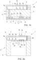
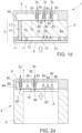
- the ceramic pressure sensor 1 comprises a ceramic body 2 and an electronic circuit 3a, 3b, 3c supported by the ceramic body 2.
- the electronic circuit 3a, 3b, 3c is provided with electrically conductive connection tracks 9.
- the ceramic body 2 in turn comprises a flexible membrane 4 made of ceramic material capable of being deformed as a result of the pressure to be sensed and a rigid support 5 made of ceramic material for supporting the flexible membrane 4.
- the electronic circuit 3a, 3b, 3c is configured to generate an electrical signal as a function of the deformation of the flexible membrane 4.
- the electronic circuit 3a, 3b, 3c comprises an analogue stage 3a for generating the electrical signal, a stage 3b for conditioning the acquired electrical signal, and a stage 3c for outputting the acquired signal and disposing an external reading of the same.
- the stage 3c is made so as to be compatible with the electrical connection methodologies available in the state of the art (it may be comprised of pins, tin-plated pads or other pads, connectors, etc).
- the materials used in this stage are often noble or however adapted to operate even in aggressive environments, sometimes preventing a protection thereon.
- the generating stage 3a comprises, for example, a Wheatstone bridge formed by a piezoresistive ink printed on the flexible membrane 4.
- the Wheatstone bridge is associated, for example, with one or more output calibration and thermal drift compensation resistances, the latter printed with ink having thermal drift characteristics suitable for the purpose.
- a protection element 6 is provided made of ceramic material permanently joined to the ceramic body 2.
- the protection element 6 delimits with the ceramic body 2 a housing chamber 7 for housing at least part of the electronic circuit 3a, 3b, 3c.
- the housing chamber 7 is hermetically closed and can be placed under vacuum, filled with an inert gas, or with air at controlled humidity.
- An electrical connection means 8 is provided for connecting the inside part of the electronic circuit 3a, 3b, 3c with the part of the electronic circuit 3a, 3b, 3c outside of the housing chamber 7.
- At least the output stage 3c is always present outside the housing chamber 7.
- the electrical connection means 8 comprises electrically conductive elements 8a, 8b, 8c, 8d passing through the wall of the housing chamber 7.
- the electrically conductive elements 8a, 8b, 8c, 8d comprise portions 8a of the conductive tracks 9 that cross the wall of the housing chamber 7 in the joining area 18 between the protection element 6 and the ceramic body 2 (solutions shown in figures 1a, and 2a , 1c, 2c which are not part of the invention).
- the output part 3c of the signal of the circuit 3a, 3b, 3c can be realised on the same face 6a of the rigid support 5 where the remaining electronic circuit 3 is positioned (solutions shown in figures 1a, and 2a which is not part of the claimed invention).
- the electrically conductive elements 8a, 8b, 8c, 8d can comprise metallised holes 8b passing through the walls of the protection element 6 (solutions shown in figures 1b, 2b , not being part of the claimed invention) or metallised holes 8c realised inside specific columns 30 inside the protection element 6 and passing through the walls of the protection element 6 (solutions shown in figures 1d, 2d , not being part of the claimed invention), the columns 30 being able to be realised in a single piece with the protection element 6.
- the electrically conductive elements 8a, 8b, 8c, 8d can comprise pins 8d inside the protection element 6 and extending through holes 31 passing through the walls of the protection element 6 (solutions shown in figures 1e, 2e , not being part of the claimed invention).
- the pins 8d can be soldered to pads provided between the discrete elements of the conditioning circuit 3b.
- the holes 31 can then be closed with an appropriate solder bead 32 around each of them.
- the ends of the pins 8d outside the housing chamber 7 constitute the signal outputting stage 3c.
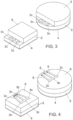
- the protection element 6 is a concave element having a flat open base 6a.
- the protection element 6 is entirely positioned inside the perimeter of a flat face 14, 19 of the ceramic body 2. Therefore, in practice, with reference to the figures, the dimensions of the protective element 6 are contained inside the vertical extension upwards of the side walls of the ceramic body 2.
- the join of the protection element 6 to the ceramic body 2 is made by soldering, e.g. SMT (surface mounting technology) or by gluing with resin or low melting point glass.
- soldering e.g. SMT (surface mounting technology) or by gluing with resin or low melting point glass.
- the ceramic material for example but not necessarily alumina based, is selected so as to give the protection element 6 suitable temperature resistance and stability, rigidity and mechanical and chemical strength properties.
- a flat ceramic pressure sensor 1 is illustrated wherein the ceramic body 2 is formed by two distinct pieces mutually connected both electrically and mechanically, one defining the flexible membrane 4 and the other the support 5.
- the two pieces are formed by two overlapping flat sheets of different thicknesses oriented with their main lying plane parallel.
- the sheets may have a circular or polygonal shape.
- the thinnest sheet defines the flexible membrane 4 and the thickest sheet defines the support 5.
- the support 5 is provided with through holes 10 having an electrically conductive coating 17, for example made of metal, for the electrical connection between the analogue generating stage 3a and the conditioning stage 3b.
- the mechanical connection system appropriately keeps the main adjacent faces of the flexible membrane 4 and the support 5 distanced.
- the mechanical connection system comprises a bead of adhesive 11 of a certain thickness, e.g. glass, which extends along a closed path so as to delimit with the main adjacent faces 13, 15 of the flexible membrane 4 and the support 5 a closed space 12 that contains the analogue stage 3a for generating the electrical signal.
- a bead of adhesive 11 of a certain thickness, e.g. glass which extends along a closed path so as to delimit with the main adjacent faces 13, 15 of the flexible membrane 4 and the support 5 a closed space 12 that contains the analogue stage 3a for generating the electrical signal.
- various beads 11 of adhesive can be provided, one around the other.
- the innermost bead 11 also delimits the flexible area of the membrane 4.
- the sheets that form the membrane 4 and the support 5 are made of ceramic material, for example but not exclusively alumina.
- the electrically conductive tracks of the electronic circuit 3a, 3b, 3c and the related components are printed on the membrane 4 and on the support 5, e.g. for the signal generating stage 3a the resistances of the resistive bridge are printed on the main face 13 of the membrane 4 adjacent to the support 5, for the conditioning stage the resistance for resetting the resistive bridge, PTC or NTC for correcting the heat drift of the sensor, and the resistances for correcting the sensitivity of the cell are printed on the main face 14 of the support 5 opposite the membrane 4.
- Such resistances can also be printed on the main face 13. Simultaneously to such elements, additional elements can be printed, e.g. sensitive to temperature variation.
- the conditioning stage 3b may also not comprise any resetting or compensation resistances, particularly if discrete components are to be used, suitable for the digital calibration of the signal.
- the pressurised fluid acts on the main face 21 of the membrane 4, opposite the one on which the electrical signal generating stage 3a is positioned (shown by an arrow in figures 1a and 1b , 1c , 1d , 1e , which are not part of the claimed invention).
- the conductive tracks 9 are also printed on the main face 14 of the support 5 opposite the membrane 4.
- the adhesive glass 11 for their mechanical join is also printed onto the main adjacent faces 13, 15 of the membrane 4 and of the support 5.
- Each printing operation may be followed by a sintering step in the oven.
- the coupling takes place by overlapping the membrane 4 and the support 5 so that the glass areas 16 are overlapped becoming one piece.
- the discrete components of the conditioning stage 3b, 3c are assembled such as, for example, condensers, transistors, integrated electronic circuits and connectors, with or without packages such as chip&wire or CSP (chip scale packages).
- the protection element 6 is applied on the main face 14 of the support 5 opposite the membrane 4.
- the mechanical join and any electrical join between the protective element 6 and the above-described parts of the sensor can be performed in various ways, each of which is valid and provides the possibility for the housing chamber 7 to be hermetic.
- the protection element 6 can be soldered with SMT technology, having a base of the flat walls to face pads suitably provided on the main face 14.
- the electrical join is performed at the same time as the mechanical one, suitably providing the soldering points.
- low melting point glass can be used, in a similar way to what is described for the join between the membrane and the support, both in relation to the mechanical join and the electrical one.
- resins may be used, possibly preformed or deposited on one or both of the faces in contact.
- the mechanical and electrical join can be performed simultaneously, as long as electrically conductive resins are used in the electrical contact areas.
- a non-conductive resin can also be used.
- the use of two different resins requires them to have a compatible polymerisation process.
- the base 6a of the protection element 6 for that purpose may have grooves 6b in which the conductive tracks 9 pass, but alternatively it is possible not to provide such grooves as the thickness of the tracks is negligible with respect to the thickness of the bead of material in relation to the join of the protection element 6 to the support 5. Further, as glass has a certain fluidity, it can balance such thicknesses, thus realising a uniform bead also in the areas overlapping with the conductive tracks 9.
- the wall of the protection element 6 is arranged straddling the electrically conductive tracks 9 that are therefore able to conduct the electrical signal of the electronic circuit outside the housing chamber 7.
- a monolithic ceramic pressure sensor 1 is illustrated wherein the ceramic body 2 is formed in a single piece that defines the flexible membrane 4 in a thinner area thereof and the support 5 in an increased thickness area thereof.
- the parts 3a, 3b of the electronic circuit 3a, 3b, 3c are fully positioned on the main face 19 of the membrane 4 opposite the main face 20 of the membrane 4 on which the pressurised fluid acts (shown by an arrow in figures 2a - 2e ,_not being part of the claimed invention).
- the realisation of the sensor 1 illustrated in figures 2a - 2e not being part of the invention preferably uses hybrid thick-film technology with the screen printing method.
- the ceramic body 2 is made of ceramic material, e.g. alumina.
- the electrically conductive tracks of the electronic circuit 3a, 3b, 3c and the related components are printed on the main face 19 of the membrane 4, e.g. for the generating stage 3a the resistances of the resistive bridge are printed, for the conditioning stage the resistance for resetting the resistive bridge, PTC or NTC for correcting the heat drift of the sensor, and the resistances for correcting the sensitivity of the cell are printed. Simultaneously to such elements, additional elements can be printed, e.g. sensitive to temperature variation.
- the conditioning stage 3b may also not comprise any resetting or compensation resistances, particularly if discrete components are to be used, suitable for the digital calibration of the signal.
- the conductive tracks 9 are also printed on the main face 19 of the membrane 4.
- Each printing operation may be followed by a sintering step in the oven.
- the discrete components of the conditioning stage 3b are mounted such as condensers, transistors, integrated electronic circuits and connectors.
- the protection element 6 is applied on the main face 19 of the membrane 4.
- the protection element 6 is applied with analogous methods to those described above for the flat ceramic sensor.
- the wall of the protection element 6 is arranged straddling the electrically conductive tracks 9 that are therefore able to conduct the electrical signal of the electronic circuit outside the housing chamber 7.
- the base 6a of the protection element 6 for that purpose has grooves 6b in which the conductive tracks 9 pass.
- the invention provides a new and more efficient method of protecting the electronic components mounted on the ceramic body 2.
- the protection is due to the ceramic element 6 that can have a variable shape and size, and that is realised such as to have a housing chamber 7 inside it of suitable dimensions to contain the objects to be protected.
- the objects to be protected may be electronic (microcontrollers, resistances, etc%), analogue parts of the sensor (inks of various kinds) or connectors, pads, pins or the like.
- any object of a suitable size and shape to be contained in the housing chamber 7 can be protected.
- the ceramic element 6 is, as mentioned, coupled permanently to the ceramic body 2 so as to make the contents of the sensor 1 hermetic.
- the ceramic element 6 further also cooperates to realise the electrical connection towards the outside of the sensor 1.
- the sensor thus realised has all the advantages of ceramic described above from a chemical, thermal and mechanical point of view. Through the invention, it becomes not strictly necessary to introduce housings or other protection elements of another kind.
- the material of the ceramic body 2 may be different from that of the ceramic protection element 6 but compatible with the described processes.
Landscapes
- Physics & Mathematics (AREA)
- General Physics & Mathematics (AREA)
- Chemical & Material Sciences (AREA)
- Analytical Chemistry (AREA)
- Measuring Fluid Pressure (AREA)
Claims (1)
- Capteur de pression en céramique (1) comprenant un corps en céramique (2) constitué d'une membrane souple (4) en matériau céramique capable de se déformer sous l'effet de la pression à détecter et d'un support rigide (5) en matériau céramique destiné à soutenir la membrane souple (4), ledit corps en céramique (2) est formé de deux pièces distinctes reliées entre elles électriquement et mécaniquement, l'une définissant la membrane souple (4) et l'autre le support rigide (5), lesdites deux pièces distinctes étant formées de deux feuilles plates superposées d'épaisseurs différentes orientées avec leur plan principal parallèle, et un circuit électronique (3a, 3b, 3c) supporté par le corps céramique (2) et comprenant des pistes de connexion électriquement conductrices (9) et un pont résistif sérigraphiés sur ladite membrane souple (4) et les pistes électriquement conductrices (9) sérigraphiées sur une face plane (14) dudit support rigide (5), ledit circuit électronique (3a, 3b, 3c) étant configuré pour générer un signal électrique en fonction de la déformation de la membrane souple (4), caractérisé en ce que le capteur de pression céramique (1) comprend en outre un élément de protection (6) en matériau céramique relié de façon permanente à face plane (14) dudit support rigide (5) opposée à la membrane (4), ledit élément de protection (6) étant entièrement positionné à l'intérieur du périmètre de ladite face plane (14) et délimitant avec ladite face plane (14) dudit support rigide (5) dudit corps céramique (2) une chambre de logement (7) pour loger au moins une partie dudit circuit électronique (3a, 3b, 3c), étant en outre prévu un moyen de connexion électrique (8) pour connecter ladite au moins une partie du circuit électronique (3a, 3a, 3b, 3c) avec l'extérieur de ladite chambre de logement (7), ledit circuit électronique (3a, 3b, 3c) comprenant un étage analogique (3a) pour générer le signal électrique, un étage de conditionnement (3b) pour conditionner le signal électrique acquis comprenant des composants discrets positionnés dans ladite chambre de logement (7) sur ladite face plate (14) dudit support rigide (5) dudit corps en céramique (2), et un étage de sortie (3c) pour la sortie du signal acquis et la disposition d'une lecture externe de celui-ci, ledit étage de sortie (3c) étant positionné à l'extérieur de ladite chambre de logement (7) sur ladite face plane (14) dudit support rigide (5), lesdites pistes conductrices électriques (9) sérigraphiées sur ledit support rigide (5) comprenant les pistes conductrices électriques (9) dudit étage de conditionnement (3b) et ledit étage de sortie (3c) sérigraphié sur ladite face plane (14) dudit support rigide (5), ledit moyen de connexion électrique (8) comprend des parties (8a) desdites pistes conductrices d'électricité (9) qui traversent la paroi de la chambre de logement (7) dans une zone de jonction (18) entre l'élément de protection (6) et le support rigide (5) du corps en céramique (2).
Applications Claiming Priority (2)
| Application Number | Priority Date | Filing Date | Title |
|---|---|---|---|
| IT102017000103447A IT201700103447A1 (it) | 2017-09-15 | 2017-09-15 | Sensore di pressione ceramico |
| PCT/EP2018/072497 WO2019052784A1 (fr) | 2017-09-15 | 2018-08-21 | Capteur de pression en céramique |
Publications (3)
| Publication Number | Publication Date |
|---|---|
| EP3658877A1 EP3658877A1 (fr) | 2020-06-03 |
| EP3658877B1 true EP3658877B1 (fr) | 2023-08-16 |
| EP3658877C0 EP3658877C0 (fr) | 2023-08-16 |
Family
ID=60991440
Family Applications (1)
| Application Number | Title | Priority Date | Filing Date |
|---|---|---|---|
| EP18753430.0A Active EP3658877B1 (fr) | 2017-09-15 | 2018-08-21 | Capteur de pression en céramique |
Country Status (4)
| Country | Link |
|---|---|
| EP (1) | EP3658877B1 (fr) |
| CN (1) | CN111094923B (fr) |
| IT (1) | IT201700103447A1 (fr) |
| WO (1) | WO2019052784A1 (fr) |
Families Citing this family (6)
| Publication number | Priority date | Publication date | Assignee | Title |
|---|---|---|---|---|
| US11385118B2 (en) | 2018-12-07 | 2022-07-12 | Vitesco Technologies USA, LLC | Pressure sensor with external vertical electrical interconnection system |
| CN113405697A (zh) * | 2020-03-16 | 2021-09-17 | 深圳聚德寿科技有限公司 | 一种方形陶瓷电容式压力传感器 |
| CN112563145A (zh) * | 2020-11-26 | 2021-03-26 | 娄底市安地亚斯电子陶瓷有限公司 | 一种汽车制剂压力应变器陶瓷电路制备方法 |
| CN114112122B (zh) * | 2021-11-30 | 2024-03-15 | 无锡胜脉电子有限公司 | 高精度陶瓷压力传感器 |
| CN115711695B (zh) * | 2022-10-13 | 2023-11-21 | 无锡盛赛传感科技有限公司 | 金属基陶瓷压力传感器、其制备工艺及制备工装 |
| CN118518064B (zh) * | 2024-06-17 | 2025-08-01 | 江西万年芯微电子有限公司 | 基于注塑成型的传感器紧固件、传感器及注塑加工方法 |
Citations (3)
| Publication number | Priority date | Publication date | Assignee | Title |
|---|---|---|---|---|
| JPS61253437A (ja) * | 1985-05-03 | 1986-11-11 | Nippon Denso Co Ltd | 半導体圧力センサ |
| US20150219514A1 (en) * | 2014-02-05 | 2015-08-06 | Mgi Coutier | Pressure and temperature determining device, pressure and temperature sensor comprising such a device and method for manufacturing such a device |
| EP3002572A2 (fr) * | 2014-09-30 | 2016-04-06 | Nagano Keiki Co., Ltd. | Dispositif de mesure de quantité physique |
Family Cites Families (8)
| Publication number | Priority date | Publication date | Assignee | Title |
|---|---|---|---|---|
| US4399707A (en) * | 1981-02-04 | 1983-08-23 | Honeywell, Inc. | Stress sensitive semiconductor unit and housing means therefor |
| DE102008054987A1 (de) * | 2008-12-19 | 2010-06-24 | Endress + Hauser Gmbh + Co. Kg | Drucksensor |
| DE102012213572A1 (de) * | 2012-08-01 | 2014-02-06 | Ifm Electronic Gmbh | Kapazitiver Drucksensor |
| US9116057B2 (en) * | 2013-02-27 | 2015-08-25 | Honeywell International Inc. | Integrated reference vacuum pressure sensor with atomic layer deposition coated input port |
| DE102013105132A1 (de) * | 2013-05-17 | 2014-11-20 | Endress + Hauser Gmbh + Co. Kg | Keramische Druckmesszelle und Verfahren zu ihrer Herstellung |
| CN103487176B (zh) * | 2013-09-24 | 2015-07-08 | 华进半导体封装先导技术研发中心有限公司 | 一种压力传感器的封装结构及方法 |
| FR3032791B1 (fr) * | 2015-02-18 | 2018-09-07 | L'essor Francais Electronique | Capteur de pression miniature a membrane metallique et procede de fabrication |
| JP6410105B2 (ja) * | 2015-09-18 | 2018-10-24 | Smc株式会社 | 圧力センサ及びその製造方法 |
-
2017
- 2017-09-15 IT IT102017000103447A patent/IT201700103447A1/it unknown
-
2018
- 2018-08-21 WO PCT/EP2018/072497 patent/WO2019052784A1/fr not_active Ceased
- 2018-08-21 CN CN201880059109.9A patent/CN111094923B/zh active Active
- 2018-08-21 EP EP18753430.0A patent/EP3658877B1/fr active Active
Patent Citations (3)
| Publication number | Priority date | Publication date | Assignee | Title |
|---|---|---|---|---|
| JPS61253437A (ja) * | 1985-05-03 | 1986-11-11 | Nippon Denso Co Ltd | 半導体圧力センサ |
| US20150219514A1 (en) * | 2014-02-05 | 2015-08-06 | Mgi Coutier | Pressure and temperature determining device, pressure and temperature sensor comprising such a device and method for manufacturing such a device |
| EP3002572A2 (fr) * | 2014-09-30 | 2016-04-06 | Nagano Keiki Co., Ltd. | Dispositif de mesure de quantité physique |
Also Published As
| Publication number | Publication date |
|---|---|
| CN111094923A (zh) | 2020-05-01 |
| CN111094923B (zh) | 2023-02-28 |
| EP3658877C0 (fr) | 2023-08-16 |
| WO2019052784A1 (fr) | 2019-03-21 |
| IT201700103447A1 (it) | 2019-03-15 |
| EP3658877A1 (fr) | 2020-06-03 |
Similar Documents
| Publication | Publication Date | Title |
|---|---|---|
| EP3658877B1 (fr) | Capteur de pression en céramique | |
| EP2834608B1 (fr) | Procédé de fabrication d'un capteur de pression en céramique | |
| US5150275A (en) | Capacitive pressure sensor | |
| US4177496A (en) | Capacitive pressure transducer | |
| US8024978B2 (en) | Media isolated pressure transducer having boss comprising single metal diaphragm | |
| US4388668A (en) | Capacitive pressure transducer | |
| EP3252449B1 (fr) | Dispositif de détection de charge miniaturisé présentant une faible sensibilité aux contraintes d'emballage thermomécaniques, en particulier capteur de pression et de force | |
| US4426673A (en) | Capacitive pressure transducer and method of making same | |
| JP4208295B2 (ja) | 組合せ式流体圧力および温度センサ装置 | |
| US4735098A (en) | Dual diaphragm differential pressure transducer | |
| EP2120029B1 (fr) | Capteur de pression à compensation ASIC avec fixation du puce de détection par soudage | |
| JPH10148591A (ja) | 圧力検出装置 | |
| GB1563894A (en) | Capacitive pressure transducer and method for making same | |
| JP2007518108A (ja) | セラミック・オン・メタル圧力変換器 | |
| CN109211458B (zh) | 压力传感器组件 | |
| EP2720019A1 (fr) | Transducteur de pression utilisant un diaphragme en céramique | |
| US6324914B1 (en) | Pressure sensor support base with cavity | |
| US5034848A (en) | Low pressure sensor | |
| JPH11326088A (ja) | 圧力センサとその製造方法 | |
| EP4214483B1 (fr) | Capteur de pression plat en céramique et procédé de fabrication correspondant | |
| EP3842779B1 (fr) | Capteurs de pression sans fil | |
| WO2025027489A1 (fr) | Dispositif de capteur de pression | |
| CN119618429A (zh) | 压力传感芯片、压力传感器及压力传感器的校准方法 | |
| Sabetti et al. | Automotive pressure transducer for underhood applications | |
| JPH01136041A (ja) | 静電容量式荷重センサ |
Legal Events
| Date | Code | Title | Description |
|---|---|---|---|
| STAA | Information on the status of an ep patent application or granted ep patent |
Free format text: STATUS: UNKNOWN |
|
| STAA | Information on the status of an ep patent application or granted ep patent |
Free format text: STATUS: THE INTERNATIONAL PUBLICATION HAS BEEN MADE |
|
| PUAI | Public reference made under article 153(3) epc to a published international application that has entered the european phase |
Free format text: ORIGINAL CODE: 0009012 |
|
| STAA | Information on the status of an ep patent application or granted ep patent |
Free format text: STATUS: REQUEST FOR EXAMINATION WAS MADE |
|
| 17P | Request for examination filed |
Effective date: 20200226 |
|
| AK | Designated contracting states |
Kind code of ref document: A1 Designated state(s): AL AT BE BG CH CY CZ DE DK EE ES FI FR GB GR HR HU IE IS IT LI LT LU LV MC MK MT NL NO PL PT RO RS SE SI SK SM TR |
|
| AX | Request for extension of the european patent |
Extension state: BA ME |
|
| RIN1 | Information on inventor provided before grant (corrected) |
Inventor name: FACCHETTI, FERMO Inventor name: MAY, ROBERTO Inventor name: LEMMA, FEDERICO DOMENICO |
|
| DAV | Request for validation of the european patent (deleted) | ||
| DAX | Request for extension of the european patent (deleted) | ||
| STAA | Information on the status of an ep patent application or granted ep patent |
Free format text: STATUS: EXAMINATION IS IN PROGRESS |
|
| 17Q | First examination report despatched |
Effective date: 20210302 |
|
| GRAP | Despatch of communication of intention to grant a patent |
Free format text: ORIGINAL CODE: EPIDOSNIGR1 |
|
| STAA | Information on the status of an ep patent application or granted ep patent |
Free format text: STATUS: GRANT OF PATENT IS INTENDED |
|
| INTG | Intention to grant announced |
Effective date: 20230411 |
|
| GRAS | Grant fee paid |
Free format text: ORIGINAL CODE: EPIDOSNIGR3 |
|
| GRAA | (expected) grant |
Free format text: ORIGINAL CODE: 0009210 |
|
| STAA | Information on the status of an ep patent application or granted ep patent |
Free format text: STATUS: THE PATENT HAS BEEN GRANTED |
|
| P01 | Opt-out of the competence of the unified patent court (upc) registered |
Effective date: 20230612 |
|
| AK | Designated contracting states |
Kind code of ref document: B1 Designated state(s): AL AT BE BG CH CY CZ DE DK EE ES FI FR GB GR HR HU IE IS IT LI LT LU LV MC MK MT NL NO PL PT RO RS SE SI SK SM TR |
|
| RAP4 | Party data changed (patent owner data changed or rights of a patent transferred) |
Owner name: KOLEKTOR MICROTEL S.R.L. |
|
| REG | Reference to a national code |
Ref country code: CH Ref legal event code: EP Ref country code: DE Ref legal event code: R096 Ref document number: 602018055479 Country of ref document: DE |
|
| REG | Reference to a national code |
Ref country code: IE Ref legal event code: FG4D |
|
| U01 | Request for unitary effect filed |
Effective date: 20230828 |
|
| U07 | Unitary effect registered |
Designated state(s): AT BE BG DE DK EE FI FR IT LT LU LV MT NL PT SE SI Effective date: 20230904 |
|
| P04 | Withdrawal of opt-out of the competence of the unified patent court (upc) registered |
Effective date: 20230830 |
|
| U20 | Renewal fee for the european patent with unitary effect paid |
Year of fee payment: 6 Effective date: 20230912 |
|
| PG25 | Lapsed in a contracting state [announced via postgrant information from national office to epo] |
Ref country code: GR Free format text: LAPSE BECAUSE OF FAILURE TO SUBMIT A TRANSLATION OF THE DESCRIPTION OR TO PAY THE FEE WITHIN THE PRESCRIBED TIME-LIMIT Effective date: 20231117 |
|
| PG25 | Lapsed in a contracting state [announced via postgrant information from national office to epo] |
Ref country code: IS Free format text: LAPSE BECAUSE OF FAILURE TO SUBMIT A TRANSLATION OF THE DESCRIPTION OR TO PAY THE FEE WITHIN THE PRESCRIBED TIME-LIMIT Effective date: 20231216 |
|
| PG25 | Lapsed in a contracting state [announced via postgrant information from national office to epo] |
Ref country code: RS Free format text: LAPSE BECAUSE OF FAILURE TO SUBMIT A TRANSLATION OF THE DESCRIPTION OR TO PAY THE FEE WITHIN THE PRESCRIBED TIME-LIMIT Effective date: 20230816 Ref country code: NO Free format text: LAPSE BECAUSE OF FAILURE TO SUBMIT A TRANSLATION OF THE DESCRIPTION OR TO PAY THE FEE WITHIN THE PRESCRIBED TIME-LIMIT Effective date: 20231116 Ref country code: IS Free format text: LAPSE BECAUSE OF FAILURE TO SUBMIT A TRANSLATION OF THE DESCRIPTION OR TO PAY THE FEE WITHIN THE PRESCRIBED TIME-LIMIT Effective date: 20231216 Ref country code: HR Free format text: LAPSE BECAUSE OF FAILURE TO SUBMIT A TRANSLATION OF THE DESCRIPTION OR TO PAY THE FEE WITHIN THE PRESCRIBED TIME-LIMIT Effective date: 20230816 Ref country code: GR Free format text: LAPSE BECAUSE OF FAILURE TO SUBMIT A TRANSLATION OF THE DESCRIPTION OR TO PAY THE FEE WITHIN THE PRESCRIBED TIME-LIMIT Effective date: 20231117 |
|
| PG25 | Lapsed in a contracting state [announced via postgrant information from national office to epo] |
Ref country code: PL Free format text: LAPSE BECAUSE OF FAILURE TO SUBMIT A TRANSLATION OF THE DESCRIPTION OR TO PAY THE FEE WITHIN THE PRESCRIBED TIME-LIMIT Effective date: 20230816 |
|
| PG25 | Lapsed in a contracting state [announced via postgrant information from national office to epo] |
Ref country code: ES Free format text: LAPSE BECAUSE OF FAILURE TO SUBMIT A TRANSLATION OF THE DESCRIPTION OR TO PAY THE FEE WITHIN THE PRESCRIBED TIME-LIMIT Effective date: 20230816 |
|
| PG25 | Lapsed in a contracting state [announced via postgrant information from national office to epo] |
Ref country code: SM Free format text: LAPSE BECAUSE OF FAILURE TO SUBMIT A TRANSLATION OF THE DESCRIPTION OR TO PAY THE FEE WITHIN THE PRESCRIBED TIME-LIMIT Effective date: 20230816 Ref country code: RO Free format text: LAPSE BECAUSE OF FAILURE TO SUBMIT A TRANSLATION OF THE DESCRIPTION OR TO PAY THE FEE WITHIN THE PRESCRIBED TIME-LIMIT Effective date: 20230816 Ref country code: ES Free format text: LAPSE BECAUSE OF FAILURE TO SUBMIT A TRANSLATION OF THE DESCRIPTION OR TO PAY THE FEE WITHIN THE PRESCRIBED TIME-LIMIT Effective date: 20230816 Ref country code: CZ Free format text: LAPSE BECAUSE OF FAILURE TO SUBMIT A TRANSLATION OF THE DESCRIPTION OR TO PAY THE FEE WITHIN THE PRESCRIBED TIME-LIMIT Effective date: 20230816 Ref country code: SK Free format text: LAPSE BECAUSE OF FAILURE TO SUBMIT A TRANSLATION OF THE DESCRIPTION OR TO PAY THE FEE WITHIN THE PRESCRIBED TIME-LIMIT Effective date: 20230816 |
|
| REG | Reference to a national code |
Ref country code: DE Ref legal event code: R097 Ref document number: 602018055479 Country of ref document: DE |
|
| REG | Reference to a national code |
Ref country code: IE Ref legal event code: MM4A |
|
| PG25 | Lapsed in a contracting state [announced via postgrant information from national office to epo] |
Ref country code: MC Free format text: LAPSE BECAUSE OF FAILURE TO SUBMIT A TRANSLATION OF THE DESCRIPTION OR TO PAY THE FEE WITHIN THE PRESCRIBED TIME-LIMIT Effective date: 20230816 |
|
| PLBE | No opposition filed within time limit |
Free format text: ORIGINAL CODE: 0009261 |
|
| STAA | Information on the status of an ep patent application or granted ep patent |
Free format text: STATUS: NO OPPOSITION FILED WITHIN TIME LIMIT |
|
| PG25 | Lapsed in a contracting state [announced via postgrant information from national office to epo] |
Ref country code: IE Free format text: LAPSE BECAUSE OF NON-PAYMENT OF DUE FEES Effective date: 20230821 |
|
| 26N | No opposition filed |
Effective date: 20240517 |
|
| GBPC | Gb: european patent ceased through non-payment of renewal fee |
Effective date: 20231116 |
|
| PG25 | Lapsed in a contracting state [announced via postgrant information from national office to epo] |
Ref country code: IE Free format text: LAPSE BECAUSE OF NON-PAYMENT OF DUE FEES Effective date: 20230821 |
|
| U20 | Renewal fee for the european patent with unitary effect paid |
Year of fee payment: 7 Effective date: 20240802 |
|
| PG25 | Lapsed in a contracting state [announced via postgrant information from national office to epo] |
Ref country code: GB Free format text: LAPSE BECAUSE OF NON-PAYMENT OF DUE FEES Effective date: 20231116 |
|
| PG25 | Lapsed in a contracting state [announced via postgrant information from national office to epo] |
Ref country code: GB Free format text: LAPSE BECAUSE OF NON-PAYMENT OF DUE FEES Effective date: 20231116 |
|
| P05 | Withdrawal of opt-out of the competence of the unified patent court (upc) changed |
Free format text: CASE NUMBER: APP_568675/2023 Effective date: 20230904 |
|
| PG25 | Lapsed in a contracting state [announced via postgrant information from national office to epo] |
Ref country code: CY Free format text: LAPSE BECAUSE OF FAILURE TO SUBMIT A TRANSLATION OF THE DESCRIPTION OR TO PAY THE FEE WITHIN THE PRESCRIBED TIME-LIMIT; INVALID AB INITIO Effective date: 20180821 |
|
| U20 | Renewal fee for the european patent with unitary effect paid |
Year of fee payment: 8 Effective date: 20250708 |
|
| PG25 | Lapsed in a contracting state [announced via postgrant information from national office to epo] |
Ref country code: HU Free format text: LAPSE BECAUSE OF FAILURE TO SUBMIT A TRANSLATION OF THE DESCRIPTION OR TO PAY THE FEE WITHIN THE PRESCRIBED TIME-LIMIT; INVALID AB INITIO Effective date: 20180821 |
|
| PGFP | Annual fee paid to national office [announced via postgrant information from national office to epo] |
Ref country code: CH Payment date: 20250901 Year of fee payment: 8 |
|
| PG25 | Lapsed in a contracting state [announced via postgrant information from national office to epo] |
Ref country code: TR Free format text: LAPSE BECAUSE OF FAILURE TO SUBMIT A TRANSLATION OF THE DESCRIPTION OR TO PAY THE FEE WITHIN THE PRESCRIBED TIME-LIMIT Effective date: 20230816 |