EP3660558A1 - Optische struktur und authentifizierungskörper - Google Patents
Optische struktur und authentifizierungskörper Download PDFInfo
- Publication number
- EP3660558A1 EP3660558A1 EP18838018.2A EP18838018A EP3660558A1 EP 3660558 A1 EP3660558 A1 EP 3660558A1 EP 18838018 A EP18838018 A EP 18838018A EP 3660558 A1 EP3660558 A1 EP 3660558A1
- Authority
- EP
- European Patent Office
- Prior art keywords
- quantization
- phase difference
- optical structure
- layer
- light
- Prior art date
- Legal status (The legal status is an assumption and is not a legal conclusion. Google has not performed a legal analysis and makes no representation as to the accuracy of the status listed.)
- Granted
Links
Images


Classifications
-
- G—PHYSICS
- G03—PHOTOGRAPHY; CINEMATOGRAPHY; ANALOGOUS TECHNIQUES USING WAVES OTHER THAN OPTICAL WAVES; ELECTROGRAPHY; HOLOGRAPHY
- G03H—HOLOGRAPHIC PROCESSES OR APPARATUS
- G03H1/00—Holographic processes or apparatus using light, infrared or ultraviolet waves for obtaining holograms or for obtaining an image from them; Details peculiar thereto
- G03H1/26—Processes or apparatus specially adapted to produce multiple sub- holograms or to obtain images from them, e.g. multicolour technique
- G03H1/30—Processes or apparatus specially adapted to produce multiple sub- holograms or to obtain images from them, e.g. multicolour technique discrete holograms only
-
- B—PERFORMING OPERATIONS; TRANSPORTING
- B42—BOOKBINDING; ALBUMS; FILES; SPECIAL PRINTED MATTER
- B42D—BOOKS; BOOK COVERS; LOOSE LEAVES; PRINTED MATTER CHARACTERISED BY IDENTIFICATION OR SECURITY FEATURES; PRINTED MATTER OF SPECIAL FORMAT OR STYLE NOT OTHERWISE PROVIDED FOR; DEVICES FOR USE THEREWITH AND NOT OTHERWISE PROVIDED FOR; MOVABLE-STRIP WRITING OR READING APPARATUS
- B42D25/00—Information-bearing cards or sheet-like structures characterised by identification or security features; Manufacture thereof
- B42D25/30—Identification or security features, e.g. for preventing forgery
- B42D25/328—Diffraction gratings; Holograms
-
- G—PHYSICS
- G02—OPTICS
- G02B—OPTICAL ELEMENTS, SYSTEMS OR APPARATUS
- G02B5/00—Optical elements other than lenses
- G02B5/18—Diffraction gratings
- G02B5/1842—Gratings for image generation
-
- G—PHYSICS
- G02—OPTICS
- G02B—OPTICAL ELEMENTS, SYSTEMS OR APPARATUS
- G02B5/00—Optical elements other than lenses
- G02B5/18—Diffraction gratings
- G02B5/1861—Reflection gratings characterised by their structure, e.g. step profile, contours of substrate or grooves, pitch variations, materials
-
- G—PHYSICS
- G02—OPTICS
- G02B—OPTICAL ELEMENTS, SYSTEMS OR APPARATUS
- G02B5/00—Optical elements other than lenses
- G02B5/32—Holograms used as optical elements
-
- G—PHYSICS
- G03—PHOTOGRAPHY; CINEMATOGRAPHY; ANALOGOUS TECHNIQUES USING WAVES OTHER THAN OPTICAL WAVES; ELECTROGRAPHY; HOLOGRAPHY
- G03H—HOLOGRAPHIC PROCESSES OR APPARATUS
- G03H1/00—Holographic processes or apparatus using light, infrared or ultraviolet waves for obtaining holograms or for obtaining an image from them; Details peculiar thereto
- G03H1/0005—Adaptation of holography to specific applications
- G03H1/0011—Adaptation of holography to specific applications for security or authentication
-
- G—PHYSICS
- G03—PHOTOGRAPHY; CINEMATOGRAPHY; ANALOGOUS TECHNIQUES USING WAVES OTHER THAN OPTICAL WAVES; ELECTROGRAPHY; HOLOGRAPHY
- G03H—HOLOGRAPHIC PROCESSES OR APPARATUS
- G03H1/00—Holographic processes or apparatus using light, infrared or ultraviolet waves for obtaining holograms or for obtaining an image from them; Details peculiar thereto
- G03H1/02—Details of features involved during the holographic process; Replication of holograms without interference recording
- G03H1/024—Hologram nature or properties
- G03H1/0244—Surface relief holograms
-
- B—PERFORMING OPERATIONS; TRANSPORTING
- B42—BOOKBINDING; ALBUMS; FILES; SPECIAL PRINTED MATTER
- B42D—BOOKS; BOOK COVERS; LOOSE LEAVES; PRINTED MATTER CHARACTERISED BY IDENTIFICATION OR SECURITY FEATURES; PRINTED MATTER OF SPECIAL FORMAT OR STYLE NOT OTHERWISE PROVIDED FOR; DEVICES FOR USE THEREWITH AND NOT OTHERWISE PROVIDED FOR; MOVABLE-STRIP WRITING OR READING APPARATUS
- B42D25/00—Information-bearing cards or sheet-like structures characterised by identification or security features; Manufacture thereof
- B42D25/30—Identification or security features, e.g. for preventing forgery
- B42D25/36—Identification or security features, e.g. for preventing forgery comprising special materials
- B42D25/373—Metallic materials
-
- B—PERFORMING OPERATIONS; TRANSPORTING
- B42—BOOKBINDING; ALBUMS; FILES; SPECIAL PRINTED MATTER
- B42D—BOOKS; BOOK COVERS; LOOSE LEAVES; PRINTED MATTER CHARACTERISED BY IDENTIFICATION OR SECURITY FEATURES; PRINTED MATTER OF SPECIAL FORMAT OR STYLE NOT OTHERWISE PROVIDED FOR; DEVICES FOR USE THEREWITH AND NOT OTHERWISE PROVIDED FOR; MOVABLE-STRIP WRITING OR READING APPARATUS
- B42D25/00—Information-bearing cards or sheet-like structures characterised by identification or security features; Manufacture thereof
- B42D25/30—Identification or security features, e.g. for preventing forgery
- B42D25/36—Identification or security features, e.g. for preventing forgery comprising special materials
- B42D25/378—Special inks
-
- G—PHYSICS
- G03—PHOTOGRAPHY; CINEMATOGRAPHY; ANALOGOUS TECHNIQUES USING WAVES OTHER THAN OPTICAL WAVES; ELECTROGRAPHY; HOLOGRAPHY
- G03H—HOLOGRAPHIC PROCESSES OR APPARATUS
- G03H2210/00—Object characteristics
- G03H2210/40—Synthetic representation, i.e. digital or optical object decomposition
- G03H2210/45—Representation of the decomposed object
-
- G—PHYSICS
- G03—PHOTOGRAPHY; CINEMATOGRAPHY; ANALOGOUS TECHNIQUES USING WAVES OTHER THAN OPTICAL WAVES; ELECTROGRAPHY; HOLOGRAPHY
- G03H—HOLOGRAPHIC PROCESSES OR APPARATUS
- G03H2250/00—Laminate comprising a hologram layer
- G03H2250/36—Conform enhancement layer
Definitions
- the embodiment of the present invention relates to an optical structure applied as means for preventing forgery of securities and card media or of passports, visas, etc. for improving security, and relates to an authentication body including the optical structure.
- three-dimensional expression provided by the holographic technique is applied as forgery prevention means to improve security, such as a computer-generated hologram of which a light wave front is computed by a computing device, in particular.
- a computer-generated hologram can be emboss-molded for duplication. Since development processing is not necessary in this case, the computer-generated hologram is a commercially excellent technique.
- Patent Literature 1 Jpn. Pat. Appln. KOKAI Publication No. 2011-118034 ) discloses a method of showing a phantom three-dimensional object as a solid body by using anisotropic scattering of light.
- the computer hologram formed of a general kinoform because of the thin groove-like diffraction grating structure on the surface, color shift is caused due to a viewing angle if the computer hologram is reproduced with a white light in which multiple wavelengths are mixed, and an iridescent diffraction light may be obtained by diffraction in an angle determined accordance with a wavelength. This is because if a white incident light is incident, the incident light is diffracted by the structure of the equal pitch of diffraction grating, and rays of the diffraction light with different wavelengths proceed in different directions.
- Security labels for forming a hologram image is commercialized by using this rainbow color.
- the color changes in an iridescent manner based on the positional relationship between an illumination, a display, and an observer.
- holograms that appear rainbow color can be easily manufactured in recent years, and do not have a sufficient forgery prevention ability any more. Accordingly, needs for expressions in place of the rainbow color have become a market trend.
- the computer hologram formed of a general kinoform cannot be applied for preventing forgery of, for example, securities such as gift vouchers, card media such as credit cards, passport and visa, etc., brand-name products, and equipment components.
- the hologram entails a characteristic blur.
- there is a technique for eliminating a dynamic visual effect so as to reduce the blur so as to reduce the blur; however, in this case, there is a problem of it lacking any difference from general printed materials since an image of an object does not change at all despite change in visual angle.
- the computer hologram formed of a general kinoform cannot be applied for preventing forgery of, for example, securities such as gift vouchers, card media such as credit cards, passports and visas, etc., brand-name products, and equipment components; accordingly, an ink, in addition to a hologram, is generally used for authentication of these.
- An ink of this type is required to have high durability so that the ink can be used without fading even over an extended period of time. Moreover, the ink preferably does not have a color-shift effect in a specific direction, so that its color tone does not change when seen from any direction.
- Patent Literature 2 Japanese Patent No. 4916636 .
- Patent Literature 2 discloses a pigment of which color-shift effect is reduced by providing two reflection layers and using an interference color.
- a hologram with diffraction grating has an advantage that an image with a high brightness can be obtained which leads to a high eye-catching effect, and a disadvantage that the color largely changes in accordance with an angle of the label and the color development is unstable.
- Another known technique aims to realize a own color development by interference between the flat upper surface of a projecting portion and a flat surface other than the projecting portion, and to stabilize color development by scattering light at the projecting portion.
- the color development of interference between the flat upper surface of a projecting portion and a flat surface other than the projecting portion has an advantage that a color shift arising due to difference in viewpoint or location of light source is small, which provides a stable color development, and a disadvantage that stable color development necessarily involves wide diffusion, which reduces brightness. Reduction of the brightness may cause reduction of the eye-catching effect.
- the embodiments of the present invention are contrived in light of such conditions, and can overcome the color instability and reduction of brightness as defects of a conventional technique such as diffraction and interference by application of the kinoform technique.
- One of the objectives thereof is to provide an optical structure and an authentication body that includes the optical structure, wherein the optical structure can enable three-dimensional expression regardless of a light source, improve the visual quality of the iridescent color, and obtain a sparkling and blinking appearance similar to jewels in accordance with a visual angle, when displaying graphic information such as a picture or character information as forgery prevention means to improve security of, for example, securities and card media, or passports and visas.
- the other objective is to be applied to an ink preferably applied to printed materials such as securities and card media, or passports and visas, so that the ink has high durability, and to apply a kinoform which enables high brightness expression so as to provide an optical structure without a color-shift effect.
- an optical structure has a quantization phase difference structure on one surface of a quantization phase difference structure layer, wherein in the quantization phase difference structure, a plurality of quantization projecting portions in a constant size and a plurality of quantization recessed portions in a constant size are aligned, wherein a multiple diffraction region has the quantization phase difference structure where ribbed projecting portions, in which the quantization projecting portions are aligned in one direction, are arranged adjacent to and alternately with groove-like recessed portions, in which the quantization recessed portions are aligned parallel to the ribbed projecting portions, and wherein the multiple diffraction region is a quantization phase difference structure configured to reproduce a plurality of reproduction points discrete in one direction and arranged regularly.
- surface roughness of a bottom surface of the quantization recessed portions of the quantization phase difference structure is different from surface roughness of a top surface of the quantization recessed portions of the quantization phase difference structure.
- a plurality of multiple diffraction regions each corresponding to the multiple diffraction region are arranged regularly in the quantization phase difference structure.
- a direction of a spatial frequency component is determined in accordance with a direction toward which an inclined surface of a projecting structure in the multiple diffraction region faces.
- a shortest distance R from the plurality of reproduction points reproduced from the spatial frequency component to a plane where the reproduction points are provided satisfies a relationship of R > D 2 / ⁇ , where D is a length of the entire multiple diffraction region and ⁇ is a wavelength of light in the multiple diffraction region.
- light intensity distribution of the plurality of reproduction points is determined such that, among the plurality of reproduction points, a reproduction point existing in a direction in which incident light is reflected on the inclined surface of the polygon in a specular manner has a highest light intensity, and a reproduction point shifted further from the direction in which the incident light is reflected in a specular manner has a lower light intensity.
- the plurality of reproduction points are arranged at an irregular interval in a space.
- the multiple diffraction region is a cell type.
- a depth of the quantization phase difference structure is different for each of the multiple diffraction regions.
- the optical structure further includes a reflection layer on a surface of the quantization phase difference structure.
- the optical structure is included in an authentication body.
- the optical structure has a quantization phase difference structure on one surface of the quantization phase difference structure layer
- the quantization phase difference structure may have a configuration where ribbed projecting portions as one element structure, in which quantization projecting portions with a constant size are aligned in one direction, and groove-like recessed portions as the other element structure, in which quantization recessed portions with a constant size are aligned parallel to the ribbed projecting portions, are arranged adjacently and alternately, the depth from the upper surface of a ribbed projecting portion to the bottom surface of a groove-like recessed portion is constant, the structure is quantized into the element structures of the quantization projecting portion and the quantization recessed portion, the surface roughness of the bottom surface of the quantization phase difference structure is rougher than the surface roughness of the upper surface, and the diffraction light of the quantization phase difference structure reproduces multiple reproduction points discrete in one direction.
- an optical structure is produced from an optical structure obtained by laminating a peeling layer, an embossed layer, and a reflection layer on a film, wherein the embossed layer has a quantization phase difference structure, a distance from a top surface of a quantization projecting portion to a bottom surface of a quantization recessed portion is constant regardless of a position in a multiple diffraction region, and wherein a plurality of peak intensities of a spatial frequency of the quantization phase difference structure are arranged separately along one direction or a plurality of directions in the embossed layer.
- surface roughness of at least one of the top surface of the quantization projecting portion or the bottom surface of the quantization recessed portion is a 10th of the distance.
- a concave-convex direction of the quantization phase difference structure is perpendicular to an extending direction of a ribbed recessed portion and a groove-like recessed portion formed by the top surface of the quantization projecting portion and the bottom surface of the quantization recessed portion.
- the optical structure is constituted by laminating a protection layer configured to protect the reflection layer.
- the optical structure is dispersed in resin, and applied as a printable ink.
- the reflection layer is magnetic
- reflection spectra of respective structural colors of the embossed layer and the reflection layer have a peak at least in a wavelength region of 800 nm to 1000 nm, and the optical structure is further constituted by laminating an optical layer configured to reflect visible light and transmit infrared light.
- a salt adsorbent is included in at least one of the embossed layer or the protection layer.
- a number of peaks of the spatial frequency of the quantization phase difference structure is five to 200.
- the optical structure can enable three-dimensional expression regardless of a light source, improve the visual quality of the iridescent color that belong to the conventional hologram, and obtain a sparkling and blinking effect similar to jewels in accordance with a visual angle, which is different from the conventional hologram, when displaying graphic information such as a picture or character information as forgery prevention means to improve security of, for example, securities and card media, or passports and visas.
- the design is made so that light spreads centering around the specular direction on the premise for computation that the light is incident from the direction opposite from the normal direction of the carrier by 180°. Accordingly, even if the light is incident obliquely with respect to the normal direction of the carrier, the light is reflected in the direction approximately the same as a reflected direction of the light in a case where there is actually an inclined surface. Thus, the same shading of light as in a case where a phantom three-dimensional object actually exists there is observed, making it appear that a three-dimensional object exists there.
- the reflected direction of the light when the light is vertically incident on a flat surface can be specified by the quantization phase difference structure, and the light can be reflected in a plurality of directions by providing a plurality of spatial frequency components.
- This effect realizes an effect equivalent to that when the light is reflected on an object, the regular reflection component is strongly reflected, and the more the angle is shifted from the specular direction, the less the reflected light intensity becomes.
- a bright spot of shading can be generated by making the spatial frequency components discrete, which generates a sparkling effect similar to jewels.
- a plurality of multiple-diffraction regions compose the quantization phase difference structure.
- the present optical structure it is also possible to determine the direction of the spatial frequency components in accordance with the direction toward which the inclined surface of spatial frequency multiplexing faces.
- the present optical structure it is also possible to obtain an effect that the light is reflected in the direction of a reproduction point without directly viewing the reproduction point by setting a diffraction region of the light that is diffracted from the multiple-diffraction region to a Fraunhofer region.
- the present optical structure it is also possible to realize an effect of light appearing to shine on a real surface by increasing the light intensity in the specular direction and reducing the intensity of light shifted from the regular reflection.
- the present optical structure it is also possible to reflect a reproduced image with a white color in a direction of dense reproduction points; on the other hand, in a part where the reproduction points are coarse, it is possible to reproduce an iridescent reproduced image such as a conventional hologram, and to control both of a white and iridescent colors.
- the present optical structure it is also possible to set the multiple-diffraction region to a cell type.
- the present optical structure it is also possible to control a reflection color of the light in accordance with the depth of the quantization phase difference structure when the light is reflected, which enables full-color expression of a three-dimensional image.
- optical structure including the present reflection layer, it is also possible to increase the reflectivity of the light.
- the present authentication body it is possible to create three-dimensional expression without depending on a light source, improve the visual quality of the rainbow color belonging to the conventional hologram, and realize a sparkling and blinking effect similar to jewels depending on a visual angle.
- the length from the top surface of the quantization projecting portion of the quantization phase difference structure to the bottom surface of the quantization recessed portion is constant regardless of the position in the embossed layer, which enables control to make the light with a specific wavelength be reflected more easily by controlling the length.
- a plurality of peak intensities of the spatial frequency are arranged separately along one direction or a plurality of directions, thereby reducing a color-shift effect, and realizing an effect that the color tone is uniform as seen from any direction.
- the surface of at least one of the top surface of the quantization projecting portion or the bottom surface of the quantization recessed portion is rough, in which the surface roughness is equal to or less than a 10th of the length from the top surface of the quantization projecting portion to the bottom surface of the quantization recessed portion; thus, the reflected direction of the light may be slightly randomized without changing the color by adopting the quantization phase difference structure to the extent that it does not depend on the wavelength of the light.
- both the top surface of the quantization projecting portion and the bottom surface of the quantization recessed portion lack any surface roughness, when the distance from the top surface of the quantization projecting portion to the bottom surface of the quantization recessed portion slightly fluctuates with respect to a designing value due to manufacturing tolerances, there is a sensitive fluctuate in color as a structural color.
- the color as a structural color does not change much even if the length from the top surface of the quantization projecting portion to the bottom surface of the quantization recessed portion slightly changes, which leads to appeasement of the manufacturing tolerances to some extent.
- the concave-convex direction of the quantization phase difference structure having surface roughness is perpendicular to the extending direction of ribbed recessed portions and groove-like recessed portions formed by the top surface of the quantization projecting portions and the bottom surface of the quantization recessed portions; thus, the light relating to the structural color can be scattered in the vertical direction. This makes it possible to scatter the light in a direction that does not change the color tone of the structural color so as to reduce an effect of the manufacturing tolerances in the structure.
- the present optical structure includes a protection layer for protecting the reflection layer, thereby protecting the surface of the reflection layer.
- a protection layer for protecting the reflection layer, thereby protecting the surface of the reflection layer.
- the protection layer from a material having the same refractive index as the material of the embossed layer, it is also possible to uniform the structural color of the front side and the back side.
- the reflection layer has a magnetic property, which enables manufacturing of the present optical structure by a method of curing a resin after being oriented in a magnetic field in a specific direction; thus, it is also possible to control the direction of the optical structure and to provide an optical effect thereof.
- the reflectance spectrum of the structural color of the embossed layer and the reflection layer has a peak at the wavelength at least equal to or more than 800 nm and equal to or less than 1000 nm, which enables manufacturing of a printed material that looks black under visible light and the same as a printed material printed with a normal black color, but reacts to infrared light. Accordingly, by providing the present optical structure in a material such as concrete, the contrast between a cracked portion and an uncracked portion can be emphasized at the time of infrared light examination, which leads to application to degradation determination of a material such as concrete.
- Deterioration of the reflection layer due to salt in the air can be prevented by including a salt adsorbent in at least one of the embossed layer and the protection layer.
- the present optical structure has a quantization phase difference structure on one surface of the quantization phase difference structure layer.
- the quantization phase difference structure may have a configuration where ribbed projecting portions as one element structure, in which quantization projecting portions with a constant size are aligned in one direction, and groove-like recessed portions as the other element structure, in which quantization recessed portions with a constant size are aligned parallel to the ribbed projecting portions, are arranged adjacently and alternately, the depth from the upper surface of a ribbed projecting portion to the bottom surface of a groove-like recessed portion is constant, and the structure is quantized into the element structures of the quantization projecting portion and the quantization recessed portion.
- the surface roughness of the bottom portion of the quantization phase difference structure is greater than the surface roughness of the upper surface, and the diffraction light of the quantization phase difference structure reproduces a plurality of reproduction points discrete in one direction.
- FIG. 1A is a plan view showing an embodiment of a multiple diffraction region 12 in a quantization phase difference structure included in an optical structure 10 according to one embodiment of the present invention.
- FIG. 1B is a graph showing an example of peak intensities of a spatial frequency components F1 to F5 at the five reproduction points in this multiple diffraction region 12.
- the optical structure 10 has an embossed surface on one side or both sides of the embossed layer.
- the embossed surface has a multiple-diffraction region on a part or the entire surface thereof.
- a quantization phase difference structure is formed on the multiple-diffraction region.
- a plurality of quantization projecting portions with a constant size and a plurality of quantization recessed portions with a constant size are aligned.
- the light parts represent the quantization projecting portions
- the dark parts represent the quantization recessed portions.
- the quantization projecting portions and quantization recessed portions are arranged at a regular interval.
- a quantization recessed portion or a quantization projecting portion is arranged adjacently to a quantization projecting portion at a regular interval.
- a quantization projecting portion or a quantization recessed portion is arranged adjacently to a quantization recessed portion at a regular interval.
- the quantization projecting portions and the quantization recessed portions are alternately arranged one by one, or for every set of multiple quantization projecting portions and quantization recessed portions.
- the multiple diffraction region 12 may be a cell including the quantization phase difference structure.
- the ribbed projecting portions where the quantization projecting portions are aligned are arranged adjacent to and alternately with the groove-like recessed portions having an element structure where the quantization recessed portions as recessed portions of a constant size are aligned in parallel with the ribbed projecting portions, and a size of the quantization projecting portion may be from a 20th to a half of a central wavelength of a visible wavelength.
- a size of the quantization recessed portion may be from a 20th to a half of the central wavelength of the visible wavelength.
- a size of the quantization projecting portion may be from 25 to 250 nm.
- a size of the quantization recessed portion may be from 25 to 250 nm.
- the quantization projecting portion may take a square shape.
- the quantization recessed portion may take a square shape.
- a corner of the quantization projecting portion may be round.
- a corner of the quantization recessed portion may be round.
- the quantization projecting portions and the quantization recessed portions may be aligned on a imaginary grid.
- the height of the quantization projecting portion may be the same as or an integral multiple of the reference height.
- the depth of the quantization recessed portion may be the same as or an integral multiple of the reference depth.
- the reference height and the reference depth may be the same.
- the value of the integral multiple may be from 1 to 4. It may also be from 1 to 8.
- the reference height and the reference depth may be from 10 to 500 nm.
- the reproduced image of a hologram reproduced by the multiple diffraction region 12 is a group of five reproduction points
- a spatial frequency component is computed along one predetermined direction D within the plane of the multiple diffraction region 12 as shown in FIG. 1A
- the horizontal axis in FIG. 1B is a spatial frequency (1/mm), and the vertical axis is a strength of the spatial frequency component.
- the reproduced image is in an iridescent color if the discrete spatial frequency components are coarse, and the reproduced image is in a white color if the discrete spatial frequency components are dense. It is possible to show a reproduced image in an iridescent color at a certain angle direction and in a white color at other angle directions by adjusting denseness and coarseness of the distribution of the spatial frequency components.
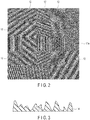
- FIG. 2 is a plan view showing an example of an optical structure 10a provided with a plurality of multiple diffraction regions 12.
- the number of the multiple diffraction region(s) 12 included in the optical structure 10 is not limited to one as in FIG. 1A , but may be plural as in FIG. 2 .
- the planar shape of each multiple diffraction region 12 shown in FIG. 1A and FIG. 2 is a rectangular shape, but shapes other than a rectangular shape may be used.
- FIG. 3 is a cross-sectional view showing a quantization phase difference structure 14.
- a reflection layer (not shown) may be provided on the surface of the quantization phase difference structure 14 of which a cross-sectional view is shown in FIG. 3 .
- the reflection layer may be translucent or opacifying.
- the reflection layer may be a reflection layer made of a metal material.
- the metal material may be Al, Ag, Sn, Cr, Ni, Cu, Au, or an alloy thereof, for example.
- a reflection layer made of metal may be an opacifying reflection layer.
- a reflection layer may be a dielectric layer of which a refractive index is different from a relief structure forming layer.
- a reflection layer may be a stacked body of dielectric layers in which adjacent layers have different refractive indices, namely, a dielectric multi-layer film. It is desirable that a dielectric layer, among the dielectric layers included in the dielectric multi-layer film, in contact with the relief structure forming layer has a different refractive index from the refractive index of the relief structure forming layer.
- the dielectric layer may be a metal compound or silicon oxide.
- the metal compound may be metal oxide, metal sulfide, or metal fluoride, for example.
- the dielectric layer may be made of TiO 2 , ZnO, Si 2 O 3 , SiO, Fe 2 O 3 , ZnS, CaF, or MgF.
- the reflection layer can be formed by a vapor-phase deposition method. A vacuum evaporation method and a sputtering method can be applied as the vapor-phase deposition method.
- the reflection layer of the dielectric layer may be translucent. The reflection layer may be from 10 to 100 nm.
- the reflection layer can be formed by using an ink.
- This ink may be an offset ink, a letterpress ink, and a gravure ink in accordance with a printing method.
- a resin ink, an oil-base ink, and a water-base ink may be used in accordance with the composition difference.
- An oxidation polymerization ink, a penetration drying ink, an evaporation drying ink, and an ultraviolet curing ink can be used in accordance with differences among drying methods.
- a reflection layer may be a functional ink in which color changes in accordance with the illumination angle or the observation angle.
- a functional ink may be an optical variable ink, a color-shifting ink, and a pearl ink.
- an inclination angle of the polygon is determined, and the quantization phase difference structure 14 corresponding to an inclined surface 15 of the inclination angle (see FIG. 5 described later) is computed.
- FIG. 4A is a front view showing a sphere 16 as an embodiment of a pseudo polygon that emerges because of the diffraction light of the quantization phase difference structure 14.
- FIG. 4B is a plan view of an optical structure 10b where a plurality of multiple diffraction regions 12 having a plurality of spatial frequency components of different directions are arranged for expressing the sphere 16 as in FIG. 4A in a pseudo manner.
- FIG. 4C is a cross-sectional view showing a positional relationship between the optical structure 10 and the sphere 16.
- FIG. 5 is a cross-sectional view showing a part of a polygon in a pseudo 3D shape for a sphere 16. It is formed of the inclined surface 15 having an inclination angle ⁇ 1 relative to the reference plane 18 of the multiple diffraction region 12.
- FIG. 5 also shows the positional relationship between the inclined surface 15 and the reproduction point 20.
- the reproduction point 20 is arranged in the specular direction of the inclined surface 15 in the embodiment of the present invention, thereby providing a visual effect in which the phantom inclined surface 15 appears to exist when the light is incident.
- a normal vector relative to the inclined surface 15 of the polygon in a phantom 3D shape constructed on the reference plane 18 is n .
- the shortest distance R from the reproduction points 20 (#1) to (#5) to the reference plane 18 satisfies the relationship as expressed R > D 2 / ⁇ in which D is the length of the entire multiple diffraction region 12, and ⁇ is the wavelength of the light in the multiple diffraction region 12.
- the light intensity distribution of a plurality of reproduction points 20 (#1) to (#5) is determined in a manner that, among the reproduction points 20 (#1) to (#5), the reproduction point 20 (#3) existing in a direction in which the incident light is reflected on the inclined surface 15 of the polygon in a specular manner has the highest light intensity, and a reproduction point shifted further from the specular direction has a lower light intensity; in other words, the light intensity reduces in the order of the reproduction point 20 (#3), reproduction point 20 (#2), and reproduction point 20 (#1), and in the order of the reproduction point 20 (#3), reproduction point 20 (#4), and reproduction point 20 (#5).
- FIG. 5 shows an embodiment in which the plurality of reproduction points 20 (#1) to (#5) are arranged at a regular interval in a space; however, the plurality of reproduction points 20 (#1) to (#5) may be arranged at an irregular interval.
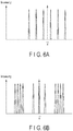
- the horizontal axis represents the aligned direction of the reproduction points 20, and the vertical axis represents the intensity of the reproduction points 20.
- a of the horizontal axis corresponds to the specular direction.
- FIG. 6A shows an embodiment in which the reproduction points 20 with the same intensity are not arranged in the specular direction, but six reproduction points 20 are arranged at a regular interval with the specular direction at the center.
- FIG. 6B shows an embodiment in which 11 reproduction points 20 with the same intensity are arranged coarsely in the vicinity of the specular direction, and densely at a position away from the specular direction.
- FIG. 6C shows an embodiment in which the reproduction points 20 are not arranged in the specular direction, but reproduction points 20 are arranged at a regular interval in a manner that the intensity is high in the vicinity of the specular direction, and the intensity is lower in a position further away from the specular direction.
- FIG. 6A shows an embodiment in which the reproduction points 20 with the same intensity are not arranged in the specular direction, but six reproduction points 20 are arranged at a regular interval with the specular direction at the center.
- FIG. 6B shows an embodiment in which 11 reproduction points 20 with the same intensity are arranged coarsely in the vicinity of the specular direction, and dense
- FIG. 6D shows an embodiment in which the reproduction points 20 are not arranged in the vicinity of the specular direction, but reproduction points 20 are arranged at a regular interval in a manner that the intensity is higher in a position further away from the specular direction, and lower in a position closer to the specular direction.
- the intensity distribution of the reproduction points 20 can be set discretionarily.
- the reproduction points 20 are arranged in a discrete manner with the specular direction at the center as shown in FIG. 5 , thereby providing a reproduced image with luster in which each polygon intricately changes in accordance with the viewpoint and the light source like jewels.
- the luster that intricately changes has a sparkling appearance.
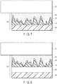
- FIG. 7 is a cross-sectional view showing an embodiment in which an optical structure 10c adheres to an adherend 22 so as to be applied to the authentication body.
- the optical structure 10c has the quantization phase difference structure 14 on a carrier 24, a reflection layer 26 made of a metal thin film is formed on the surface of the quantization phase difference structure 14, an adhesion layer 28 is provided on the surface of the reflection layer 26, and the optical structure 10c adheres to the adherend 22 via the adhesion layer 28.
- the carrier 24 is transparent so as to reduce the loss of the reflected light.
- the carrier 24 can be made of a rigid body such as glass, or a film.
- the film may be a plastic film.
- the plastic film may be a PET (polyethylene terephthalate) film, PEN (polyethylene naphthalate) film, or a PP (polypropylene) film, for example.
- a paper, a synthetic paper, a plastic multi-layer paper, a resin impregnated paper, etc. c be used as a carrier.
- the material forming the quantization phase difference structure 14 can be thermoplastic resin such as urethane resin, polycarbonate resin, polystyrene resin, polyvinyl chloride resin, etc., thermoset resin such as unsaturated polyester resin, melamine resin, epoxy resin, urethane (meta-)acrylate, polyester (meta-)acrylate, epoxy (meta-)acrylate, polyol (meta-)acrylate, melamine (meta-)acrylate, triazine (meta-)acrylate, etc., a composite thereof, or a thermoformable material having a radical polymerizable unsaturated group, for example.
- thermoplastic resin such as urethane resin, polycarbonate resin, polystyrene resin, polyvinyl chloride resin, etc.
- thermoset resin such as unsaturated polyester resin, melamine resin, epoxy resin, urethane (meta-)acrylate, polyester (meta-)acrylate, epoxy (meta-)acrylate, polyol (met
- FIG. 8 is a cross-sectional view showing another embodiment in which an optical structure 10d adheres to an adherend 22 so as to be applied to the authentication body.
- the optical structure 10d shown in FIG. 8 is different from the optical structure 10c shown in FIG. 7 in that a peeling layer 30 is provided between the carrier 24 and the quantization phase difference structure 14 for peeling off the carrier 24.
- the carrier 24 is peeled off by peeling of the peeling layer 30; thus, the carrier 24 needs not be transparent.
- the forming material of the peeling layer 30 may be resin.
- the peeling layer 30 may include a lubricant.
- the resin may include thermoplastic resin, thermoset resin, ultraviolet curable resin, and electron beam curable resin, for example.
- the resin may be acrylate resin, polyester resin, or polyamide resin.
- the lubricant may be wax such as polyethylene powder, paraffin wax, silicone, and carnauba wax. These may be applied, as the peeling layer 30, on the layer of the carrier 24. Publicly known application methods may be applied to the application.
- the application may be a gravure coat, a micro gravure coat, a die coat, or a lip coat, for example.
- the thickness of the peeling layer 30 may be within the range from 0.5 to 5 ⁇ m.
- graphic information such as a picture or character information can be the rainbow-free colors, and the appearance can have luster like jewels depending on the viewpoint and the light source. This appearance is sparkling since blinking brightness is given by blinking in viewpoint and light source. This appearance can improve security of, for example, quantization phase difference structure securities and card media, or passports and visas.
- a plurality of spatial frequency components are taken into consideration, and a plurality of reproduction points 20 are taken into consideration in accordance therewith.
- each of a quantization projecting portion and a quantization recessed portion is a square having a side of 100 nm.
- This graphic resolution is the graphic resolution of drawing on a resist of an electron beam drawing device.
- Ni sputtering is performed, and a Ni plate is produced after Ni electrocasting. From this Ni plate, emboss molding is performed to a PET film by a UV curable resin. 150 nm of Al is evaporated on the surface of the structure after emboss molding.
- a reproduced image which shines dimly in a rainbow color is reproduced.
- the reproduced image is dim because there are few scattering components and reflected light cannot be visually confirmed.
- ⁇ at this time is equal to the inclination angle of the inclined surface 15.
- ⁇ 2 in FIG. 5 is set to 90 degrees.
- the optical structure 10 is produced in the same manner as the comparative example.
- 250 by 250 multiple diffraction regions 12 constituted by quantization projecting portions and quantization recessed portions aligned on a grid of 240 ⁇ 240 are arranged; each of a quantization projecting portion and a quantization recessed portion is set to a square having a side of 100 nm; Ni sputtering is performed after drawing on a resist, a Ni plate is produced after Ni electrocasting; emboss molding is performed with this Ni plate to a PET film by UV curable resin; and 150 nm of Al is evaporated on the surface of the structure after emboss molding.
- a reproduced image shining in an iridescent color is reproduced. Its brightness is greater than the comparative example.
- the computation of the phase is performed in the present Example 2, while the number of reproduction points N is set to 91 and other conditions are not changed.
- the optical structure 10 is produced similarly to the comparative example. To sum up, 250 by 250 multiple diffraction regions 12 constituted by quantization projecting portions and quantization recessed portions aligned on a grid of 240 ⁇ 240 are arranged, and each of a quantization projecting portion and a quantization recessed portion is set to a square having a side of 100 nm, Ni sputtering is performed after drawing on a resist and Ni plate is produced after Ni electrocasting, emboss molding is performed with this Ni plate to a PET film by UV curable resin, and 150 nm of Al is evaporated on the surface of the structure after emboss molding.
- the present optical structure can realize a brighter and whiter reproduced image by increasing the number of the reproduction points, as in the comparison between the comparative example and Examples 1 and 2.
- a peeling layer, an embossed layer, and a reflection layer are laminated on a film.
- FIGS. 9A and 9B are a cross-sectional view schematically showing a configuration of an optical structure according to another embodiment of the present invention.
- an optical structure 40 is constituted by laminating a peeling layer 44, an embossed layer 46, and a reflection layer 48 on a film 42.
- a protection layer 49 for protecting the reflection layer 48 may be layered on the non-embossed layer side of the reflection layer 48.
- the carrier 42 can be a rigid body such as glass, or a film.
- the film may be plastic.
- the plastic film may be a PET (polyethylene terephthalate) film, PEN (polyethylene naphthalate) film, or a PP (polypropylene) film, for example.
- a paper, a synthetic paper, a plastic multi-layer paper, a resin impregnated paper, etc. may be used.
- the carrier may be a heat-resistant material. The heat-resistant material has small defomations and deteriorations due to heat and pressure, etc. applied when the embossed layer 46 is laminated.
- the forming material of the peeling layer 44 can be resin.
- the peeling layer 44 may include a lubricant.
- the resin may be acrylate resin, polyester resin, or polyamide resin.
- the resin may be thermoplastic resin, thermoset resin, ultraviolet curable resin, and electron beam curable resin, for example.
- the lubricant may be wax such as polyethylene powder, paraffin wax, silicone, and carnauba wax.
- the peeling layer 44 may be formed by a publicly known application method.
- the peeling layer 44 may be formed on the carrier 42 by a gravure printing method or a micro gravure method, for example.
- the thickness of the peeling layer 44 may be within the range from 0.5 to 5 ⁇ m.
- FIG. 10 is a cross-sectional view schematically showing a structure of the embossed layer 46 of the optical structure 40.
- the embossed layer 46 is in an approximately flat shape, and has a quantization phase difference structure 50 on one side.
- a length L from the upper surface 52 of the quantization projecting portion of the quantization phase difference structure 50 to the lower surface 54 of the quantization recessed portion is constant regardless of a position on the surface of the embossed layer 46.
- the upper surface 52 of the quantization projecting portion and the lower surface 54 of the quantization recessed portion can be approximately parallel to the carrier 42.
- Such embossed layer 46 modifies a color of the reflected light based on the length L.
- the concavoconvex direction of the quantization phase difference structure 50 (namely, the vertical direction in FIG.
- the embossed layer 46 has an embossed surface on one side or both sides.
- the embossed surface includes a phase angle recording region.
- a quantization phase difference structure is formed in the phase angle recording region.
- quantization projecting portions and quantization recessed portions are aligned.
- a quantization projecting portion and a quantization recessed portion has a horizontal width of the integral multiple of a unit length, and a vertical width of the integral multiple of a unit length.
- the unit length may be from a 20th to a half of the center wavelength of the visible wavelength.
- the unit length may be from 25 to 250 nm.
- the quantization projecting portions are arranged at the portion where a phase angle to be recorded is equal to or more than 0 and less than ⁇ . If the height of the quantization projecting portions is constant, the phase angle equal to or more than 0 and less than ⁇ is quantized to ⁇ /2.
- the quantization projecting portions have a quantized height corresponding to ⁇ /2. If the quantization projecting portions have a plurality of heights, the heights are quantized at an interval of ⁇ /(2 ⁇ n).
- the quantization projecting portions have respective quantized heights corresponding to respective phases.
- the quantization recessed portions are arranged at the portion where a phase angle to be recorded is equal to or more than ⁇ and less than 2n.
- the phase angle equal to or more than ⁇ and less than 2 ⁇ is quantized to 3 ⁇ /2. If there are a plurality of depths of the quantization recessed portions, the quantization is performed at an interval of ⁇ /(2 ⁇ n).
- the quantization recessed portions have respective quantized heights corresponding to respective phases.
- a wavelength of the light, which is diffracted in a specific angle because of a mutual effect of the quantization projecting portions and the quantization phase difference structure where the quantization recessed portions are aligned, is determined in accordance the spatial frequency, the incident angle, and the diffraction angle determined in accordance with the arrangement of the quantization projecting portions and the quantization recessed portions.
- space frequencies of the quantization projecting portions and the quantization recessed portions are discrete; thus, only diffraction light corresponding to the spatial frequency is diffracted. Since the diffraction light is emitted with wavelengths at a certain interval, the observed diffraction light is in a mixed color of diffraction lights with a plurality of specific wavelengths.
- the quantization recessed portions have a constant depth and the quantization projecting portions have a constant height, the reflected light on the top surfaces of the quantization projecting portions interferes with the reflected light on the bottom surface of the quantization recessed portions due to the mutual effect with the quantization phase difference structure in which the quantization recessed portions are aligned. If the quantization recessed portions have a constant depth and the quantization projecting portions have a constant height, the depth and the height may be from 100 nm to 400 ⁇ m.
- the interfering light becomes maximum when the phase difference between the reflected light of the top surface and the reflected light of the bottom surface with a uniform phase is 0 or an integral multiple of 2n, and the reflected light becomes 0 when the reflected light on the top surface and the reflected light on the bottom surface with opposite phases have the phase difference of an integer multiple of ⁇ and interfere with and annihilate each other.
- the reflected light seamlessly varies from the maximum to 0 between the phase difference when the phases are uniform and the phase difference when the phases are opposite. Since the phase difference is proportional to the wavelength of the reflected light, the intensity of the reflected light with each wavelength caused by the interference sequentially varies. Accordingly, the reflected light caused by the interference is in a specific band.
- a quantization phase difference structure in which the quantization recessed portions have a constant depth and the quantization projecting portions also have a constant height, emits reflected light by these interference and diffraction.
- a quantization phase difference structure in which the quantization recessed portions have a constant depth and the quantization projecting portions also have a constant height, selectively emits reflected light in a band of the interfering light among the diffraction light.
- diffraction light of a high level equal to or higher than a secondary level, which is normally determined as noise is also emitted; thus, reflected light as designed cannot be obtained.
- the interfering light among the diffraction light is selectively reflected in the quantization phase difference structure of the present invention, reflected light that does not include a high-level diffraction light can be obtained.
- the top surface of the quantization projecting portion or the bottom surface of the quantization recessed portion may be a rough surface. Thereby, a necessary band of interference by the quantization phase difference structure can be ensured.
- the computing device computes a phase W (x, y) of the light from a reproduction point 220 (#a) with respect to quantization projecting portions and quantization recessed portions included in an overlapping region 190 (#1) where a computational element section 160 (#A) specified by one reproduction point 220 (#a) overlaps a phase angle recording region 180 (#a), and also in an overlapping region 190 (#2-1) where a computational element section 160 (#A) overlaps a part of a phase angle recording region 180 (#2).
- reproduction point 220 There is one reproduction point 220, or a plurality of reproduction points 220.
- the computing device further computes a phase W (x, y) of the light from a reproduction point 220 (#b) with respect to quantization projecting portions and quantization recessed portions included in an overlapping region 190 (#2) where a computational element section 160 (#B) determined another reproduction point 220 (#b) overlaps a phase angle recording region 180 (#2), as shown in FIG. 6 .
- the computing device further computes the phase angle ⁇ (x, y) based on the computed phases W (x, y), and records information of numeral values of the computed phase angle ⁇ (x, y) in the corresponding overlapping region 190 as retardation.
- W n (kx, ky) is a phase of a reproduction point n at the coordinates (kx, ky) in the computational element section 160 of the nth reproduction point
- W (x, y) is a phase at the coordinates (x, y, 0) to be recorded in the phase modulation structure
- amp n is the amplitude of the light of nth reproduction point
- i is an imaginary number
- ⁇ is the wavelength of the light when reproducing a reproduced image to be reproduced with a group of reproduction points 220
- O n (x) is a value of an x-coordinate of a reproduction point
- O n (y) is a value of an y-coordinate of a reproduction point
- O n (z) is a value of an z-coordinate of a reproduction point
- (kx, Ky, 0) are coordinates of a quantization projecting portion and a
- Phase W n (kx, ky) is obtained at all points in the computational element section 160. Since a phase of a reproduction point n is the same at the points having the same distance from the reproduction point 220, information of a computed phase can be copied for the phase of a reproduction point n. Furthermore, as will be described below, O n (z) is a value of a z-coordinate of a reproduction point; in other words, since the phase W n (kx, ky) of the reproduction points having the same distance from the recording surface has the same phase distribution, information of a computed phase can be copied for the phase W n (kx, ky).
- phase of the reproduction point 220 for recording the numeral value information in the quantization projecting portions and quantization recessed portions increases, the amount of information also increases along with the increase, and the computation time also increases. If the phase of the reproduction point 220 for recording is too large, it may decrease the contrast of the reproduced image reproduced at the reproduction point 220.
- overlapping region 190 (#2-1) in order to obtain a clearer reproduced image for the part where the phase angle recording regions 180 of a plurality of reproduction points 220 (#a, #b) overlap with each other, it is preferable that overlapping of the computational element sections 160 is small, or in other words, the number of computational element sections existing in the phase angle recording regions 180 is small.
- a phase angle recording region 180 may prevent overlapping of computational element sections 160, or in other words, may have one computational element section 160. Furthermore, if the phase angle recording region 180 has a plurality of computational element sections 160, the number of the computational element sections 160 in the phase angle recording region 180 may be set to equal to or less than 256. In this case, the computation is more efficiently performed. The number of the computational element sections 160 in the phase angle recording region 180 may be set to be equal to or less than 16. In this case, it is easier to obtain a clear reproduced image.
- Phase W (x, y) is computed with respect to the quantization projecting portions and quantization recessed portions in the overlapping region 190 where the computational element section 160 specified by the viewing angle ⁇ overlaps the phase angle recording region 180, and a phase angle ⁇ (x, y) is computed based on the Phase W (x, y).
- the upper limit of the viewing angle ⁇ is specified, and a region where the phase angle ⁇ is computed is limited to the overlapping region 190; thus, the computation time is shortened.
- the computed phase angle ⁇ is recorded as retardation in a corresponding quantization projecting portion and a quantization recessed portion in the overlapping region 190.
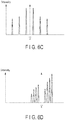
- FIG. 7 is an SEM image showing quantization projecting portions and quantization recessed portions in which phase angles ⁇ are recorded.
- the quantization projecting portions and quantization recessed portions shown in FIG. 7 are squares of which side length is d, and are two-dimensionally arranged at an arrangement interval d in both the X direction and Y direction.
- phase angle non-recording region 200 may be provided on the recording surface 140. Even if the phase angle non-recording region 200 overlaps the computational element section 160, the computing device does not perform computation, and the phase angle is not recorded in the phase angle non-recording region 200. Instead, the phase angle non-recording region 200 may record information other than the phase angle, such as information related to scatter, reflection, and diffraction characteristics of the light. Alternatively, the phase angle non-recording region 200 may be translucent, and a printing may be carried out for the phase angle non-recording region 200. This improves the designability of the phase modulation structure 240 having a recording surface.
- FIG. 10 shows the configuration where projections and recesses of the plurality of quantization phase difference structures 50 have the same pitch P; however, the configuration of the embossed layer 46 is not limited thereto.
- the embossed layer 46 may have different pitches P, different lengths L, different lengths T of the top surfaces 52 of the quantization projecting portions, and different lengths B of the bottom surfaces 54 of the quantization recessed portions.
- the embossed layer 46 has quantization phase difference structures 50 with locally different pitches P, lengths L, lengths T, and lengths B, so as to have a plurality of spatial frequency components in the quantization phase difference structures 50.
- quantization phase difference structures 50 are constituted by quantization projecting portions and quantization recessed portions of a constant size, a structure smaller than the size of the quantization projecting portions and quantization recessed portions is not formed.
- a structure of the integral multiple of a quantization projecting portion or a quantization recessed portion is formed in a region where quantization projecting portions are continuously arranged or a region where quantization recessed portions are continuously arranged.
- FIG. 11A is a plan view showing a multiple diffraction region formed by an embossed layer 46 having a quantization phase difference structure 50.
- FIG. 11A shows that a quantization phase difference structure 50 having many different pitches P is arranged over the entire surface of the embossed layer 46, similarly to FIG. 1A .
- FIG. 11B is a plan view of five spatial frequency components f1 to f5 in the multiple diffraction region of FIG. 11A .
- FIG. 11C is a figure showing peak intensities of spatial frequency components f1 to f5 shown in FIG. 11B .
- the horizontal axis represents a distance (pixels) on the plane, and the vertical axis represents gray values.
- multiple-diffraction regions which respectively have specified spatial frequency components f1 to f5 respectively corresponding to respective reproduction points arranged in a discrete manner along one predetermined direction on a plane, are arranged in the quantization phase difference structure 50 on a plane, similarly to one embodiment of the present invention.
- a plurality of spatial frequency components f1 to f5 are arranged separately in one direction.
- five spatial frequency components f1 to f5 are shown as an example.
- the number of the spatial frequency components is from 5 to 200.
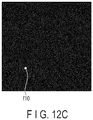
- FIGS. 12A, 12B , and 12C are plan views showing spatial frequency components different from FIG. 11B for comparison.
- Five spatial frequency components f1 to f5 shown in FIG. 11B to be compared are distributed separately in one direction, thereby restricting the range of color shift of the color of the reflected light. It is also possible to suppress decrease in brightness when viewed by eye or sensed with a measuring instrument, and suppress decrease in brightness of the reflected light, by changing the distance between adjacent spatial frequency components.
- one spatial frequency component f6 shown in FIG. 12A is linear, thereby having a higher effect for suppressing color shift than FIG. 11B ; this causes a decrease in brightness when viewed by eye or sensed with a measuring instrument, which leads to lower brightness than the case of FIG. 11B .
- each of the three spatial frequency components f7 to f9 shown in FIG. 12B is a linear spatial frequency component, the light is diffused in multiple directions. Similarly to FIG. 12A , this improves the effect to suppressing color shift than FIG. 11B ; this causes decrease in brightness when viewed through eyes or sensed with a measuring instrument, which leads to lower brightness than the case of FIG. 11B .
- the light is diffused in a single direction, but the color shift cannot be restricted.
- the embossed layer 46 may include a salt adsorbent. If the optical structure 40 includes the protection layer 49 as in FIG. 9B , at least one of the embossed layer 46 and the protection layer 49 includes a salt adsorbent.
- FIG. 13 is a micrograph obtained by observing a part of the surface of the quantization phase difference structure 50 of the embossed layer 46 with a scanning electron microscope.
- ribbed projecting portions as one element structure in which quantization projecting portions in a constant size are aligned in one direction
- groove-like recessed portions as the other element structure, in which quantization recessed portions in a constant size are aligned parallel to the ribbed projecting portions, are arranged adjacently and alternately.
- the depth from the top surface 52 of the quantization projecting portions of the ribbed projecting portions to the bottom surface 54 of the quantization recessed portions of the groove-like recessed portions is constant, and the structure is quantized into the element structures of the quantization projecting portion and the quantization recessed portion.
- the surface roughness of the bottom surface 54 of the quantization recessed portion of the quantization phase difference structure 50 is greater than the surface roughness of the top surface 52 of the quantization projecting portion, and the diffraction light of the quantization phase difference structure 50 reproduces a plurality of reproduction points discrete in one direction.
- the surface of the quantization phase difference structure 50 of the embossed layer 46 has a structure that is regular to some extent but is complicated as shown in FIG. 13 .
- the bottom surface 54 of the quantization recessed portions of the quantization phase difference structure 50 have a constant depth, and the variation in the depth of the bottom surface 54 of the quantization recessed portions is equal to or less than a 10th of the length L.
- the surface of the bottom surface 54 of the quantization recessed portion may be rough.
- the material of the embossed layer 46 can be thermoplastic resin such as urethane resin, polycarbonate resin, polystyrene resin, polyvinyl chloride resin, etc., thermoset resin such as unsaturated polyester resin, melamine resin, epoxy resin, urethane (meta-)acrylate, polyester (meta-)acrylate, epoxy (meta-)acrylate, polyol (meta-)acrylate, melamine (meta-)acrylate, triazine (meta-)acrylate, etc., a composite thereof, or a thermoformable material having a radical polymerizable unsaturated group, for example.
- thermoplastic resin such as urethane resin, polycarbonate resin, polystyrene resin, polyvinyl chloride resin, etc.
- thermoset resin such as unsaturated polyester resin, melamine resin, epoxy resin, urethane (meta-)acrylate, polyester (meta-)acrylate, epoxy (meta-)acrylate, polyol (meta-
- the reflection layer 48 may be formed by applying an ink.
- this ink may be an offset ink, a letterpress ink, a gravure ink, etc.
- this ink may be a solventless ink, an oil-based ink, or a water-based ink.
- this ink may be an oxidation polymerization ink, a penetration drying ink, an evaporation drying ink, or an ultraviolet curing ink.
- the reflection layer 48 may be a functional ink of which color shifts in accordance with the illumination angle or the observation angle.
- a functional ink an optical variable ink, a color-shifting ink, and a pearl ink can be used.
- the reflection layer 48 can be metal or a metal compound.
- the metal compound may be TiO 2 , Si 2 O 3 , SiO, Fe 2 O 3 , ZnS, etc. These metal compound has a high refractive index, and easily has high reflectivity.
- the metal may be Al, Ag, Sn, Cr, Ni, Cu, Au, etc. It is easy to increase the reflectivity of these metals.
- the reflection layer 48 may have magnetism.
- the protection layer 49 can be made of the same kind of material as the embossed layer 46.
- the protection layer 49 may be made of the same material as the embossed layer 46. If the protection layer 49 is made of the same material as the embossed layer 46, the refractive index can be set to be the same as the embossed layer 46, and thus the colors on the front and back sides of the optical structure 40 can be set to be the same.
- An optical layer (not shown) that reflects the visible light and transmits infrared light may be further laminated on the optical structure 40.
- the structural colors of the embossed layer 46 and the reflection layer 48 preferably have a reflectance spectrum that has a peak at least in the wavelength region from 800 nm to 1000 nm.
- the optical structure according to the embodiment of the present invention is produced by peeling the embossed layer 46 and the reflection layer 48, as materials for an optical structure, off of the carrier 42 of such optical structure 40 via the peeling layer 44, and making these materials for an optical structure into fine powder.
- the optical structure produced in such a manner is dispersed in resin, and applied as a printable ink.
- the length L from the top surface 52 of the quantization projecting portion of the quantization phase difference structure 50 to the bottom surface 54 of the quantization recessed portion is constant regardless of the position on the surface of the embossed layer 46, and the light of a specific wavelength can be reflected more easily by adjusting the value of the length L.
- the color shift can be reduced and the color variation along with change in the observation direction and the illumination direction can be reduced by separately arranging the peak intensities of a plurality of spatial frequency distribution f1 to f5 along one direction or a plurality of directions in a plane, as shown in FIG. 11B .
- the color-shift effect can be also reduced in the case of linearly and continuously arranging the peak intensity of the spatial frequency component f6. In this case, the brightness and saturation of the color is reduced.
- the peak intensities of the spatial frequency components f7 to f9 are set to a plurality of directions (not only one direction) in a plane as shown in FIG. 12B , there are too many reflected directions of the light, which leads to reduction in brightness.
- the embossed layer 46 has the simple diffraction grating of a single pitch P as shown in FIG. 10 ; in this case, the number of reflected directions is too small, which leads to reduction of the entire brightness.
- the surface roughness of the bottom surface 54 of the quantization recessed portion is high, which is equal to or less than a 10th of the length L.
- the light with a specific wavelength can be reflected by adjusting the length L from the top surface 52 of the quantization projecting portion to the bottom surface 54 of the quantization recessed portion; if neither the top surface 52 of the quantization projecting portion nor the bottom surface 54 of the quantization recessed portion has any surface roughness, the length L fluctuate in accordance with the tolerance relative to the designed value, thereby fluctuating the color sensitively.
- the color changing degree with respect to the length L reduces, which leads to moderation of tolerances.
- Such an effect is not limited to the effect exhibited by the surface roughness of the bottom surface 54 of the quantization recessed portion, but is also exhibited by the surface roughness of the top surface 52 of the quantization projecting portion, similarly.
- the average surface roughness of either one of the top surface 52 of the quantization projecting portion or the bottom surface 54 of the quantization recessed portion is equal to or less than a 10th of the reference length L.
- An arithmetic average roughness (Ra) can be applied to the surface roughness.
- the arithmetic average roughness (Ra) is equal to or less than 0.1.
- the roughness may be equal to or more than a 100th of the length L. In other words, the arithmetic average roughness (Ra) is equal to or more than 0.01.
- the surface roughness of the top surface 52 of the quantization projecting portion may be smaller than the surface roughness of the bottom surface 54 of the quantization recessed portion. In this case, the tolerances of the structural color can be reduced, and reduction of saturation of the structural color is suppressed. In other words, both of stability and chromogenic of the structural color and can be achieved.
- the surface roughness of the bottom surface 54 of the quantization recessed portion may be smaller than the surface roughness of the top surface 52 of the quantization projecting portion. In other words, the surface roughness of the top surface 52 of the quantization projecting portion is different from the surface roughness of the bottom surface 54 of the quantization recessed portion.
- the concave-convex direction of the quantization phase difference structure 50 (namely, the vertical direction in FIG. 10 ) is perpendicular to the extending direction of the ribbed recessed portion and the groove-like recessed portion formed by the top surface 52 of the quantization projecting portion and the bottom surface 54 of the quantization recessed portion, thereby scattering the light related to the structural color in the vertical direction in which the color tone of the light is not changed; accordingly, the optical structure according to the embodiment of the present invention can be realized even if there are manufacturing tolerances.
- the optical structure according to the embodiment to the present invention is constituted by the optical structure 40 where the protection layer 49 is laminated as shown in FIG. 9B
- the structural colors on the front and back sides of the optical structure may be set to the same by forming the protection layer 49 from a material having the same refractive index as the embossed layer 46.
- the reflection layer 48 is magnetic, it enables manufacturing by a method of curing a resin after the optical structure is oriented in a magnetic field in a specific direction; thus, it is possible to control the direction of the optical structure and to provide an optical effect deriving therefrom.
- the reflection spectra of the structural colors of the embossed layer 46 and the reflection layer 48 have a peak at least in the wavelength region from 800 to 1000 nm, it is possible to produce a printed material that looks black similarly to general printed materials printed in black under visible light but reacts to infrared light.
- the optical structure according to the embodiment of the present invention can be applied to the degradation determination of a material such as concrete. If a material to be tested such as concrete includes the optical structure according to the embodiment of the present invention, the contrast between a cracked portion and an uncracked portion can be emphasized at the time of infrared light examination.
- Deterioration of the reflection layer 48 due to salt in the air can be prevented by including a salt adsorbent in the embossed layer 46, or in at least one of the embossed layer 46 or the protection layer 49 if the protection layer 49 is provided as shown in FIG. 9B .
- An ink that does not fade even after time passes can be realized by applying flakes of the optical structure according to the embodiment of the present invention as pigments of the ink for a printed material required to have high durability. Since this ink can eliminate the color-shift effect in a specific direction, this ink can also realize a color tone that does not easily change as seen from any direction. Therefore, it is quite preferable for use as identification means for authentication for forgery of securities such as gift vouchers, credit cards, brand-name products, and equipment components.
- the ink is normally invisible to the human eye but can be detected by an infrared detector, etc. Based on this fact, the ink for infrared light can be utilized for detecting cracks of concrete with infrared light by including the ink in concrete.
- Patent Literature 3 ( WO 2007/131375 ) discloses the technique of developing colors by interference between the top surface 52 of the quantization projecting portion and the bottom surface 54 of the quantization recessed portion similarly to the quantization phase difference structure 50 shown in FIG. 13 and FIG. 14 .
- the configuration disclosed in Patent Literature 3 has a constant relief height but has uneven widths.
- the configuration disclosed in Patent Literature 3 has a disadvantage that bad formation easily occurs in wide portions and narrow portions.
- such bad formation does not occur since the relief width is constant.
- the image is not in a rainbow color as in the conventional diffraction grating, as shown in FIG. 15 , and a brighter image than the image realized in the Patent Literature 3 can be obtained.
- the embossed layer 46 is designed. Specifically, 90 spatial frequency components are separately arranged on the quantization phase difference structure 50, and the embossed layer 46 is designed so that adjacent rays of light are about 2 degrees apart and the light spreads in a direction of 180 degrees in a planar manner when the light is vertically incident.
- a positive resist having a film thickness of 0.6 ⁇ m is applied on a glass original plate, and the quantization phase difference structure 50 is drawn on the positive resist surface by using an electron beam drawing device.
- the dose amount of positive resist to be applied is determined by adjustment so that the length of the positive resist is around 220 nm.
- a conductive thin film of Ni is provided by a sputtering method on the glass original plate on the side where the quantization phase difference structure 50 is formed by image development. Then, the conductive thin film is plated with Ni, and the conductive thin film of Ni is peeled off the glass original plate to produce a duplicate plate, thereby obtaining an embossing plate.
- a peeling layer 44 is provided by applying Denka Poval (registered trademark) (polyvinyl alcohol) one surface of a polyester film (Toray industries, Inc., product name: "Lumirror 19528”), which has a thickness of 19 ⁇ m and used as the carrier 42, by the gravure coating method so that the film thickness of Denka Poval after drying is 2 ⁇ m.
- Denka Poval registered trademark
- polyester film Toray industries, Inc., product name: "Lumirror 19528”
- the embossed layer 46 is formed on the peeling layer 44 by applying UV-curable resin ("POLYSTER” produced by Washin Chemical Industry CO., LTD.) to have a film thickness of 2 ⁇ m on the peeling layer 44, pressing the above-described embossing plate on the application surface, and irradiating ultraviolet light of 200 mJ/cm 2 from a side of the surface of the polyester film as the carrier 42, on which the peeling layer 44 is not applied, to cure the UV-curable resin.
- This embossing plate is peeled off, thereby forming the embossed layer 46 including the quantization phase difference structure 50 on the peeling layer 44.
- the reflection layer 48 covering the embossed layer 46 is formed by forming an Al deposited thin layer of a film thickness of 50 nm over the entire surface of the embossed layer 46.
- the protection layer 49 is formed by applying UV-curable resin to have a film thickness of 2 ⁇ m again on the reflection layer 48 ("POLYSTER 200" produced by Washin Chemical Industry CO., LTD.). In this manner, the embossed layer 46 and the protection layer 49 are formed of the same material.
- An optical structure formed in this manner is immersed in a liquid to dissolve the peeling layer 44, thereby separating an optical structure material including the embossed layer 46, the reflection layer 48, and the protection layer 49 from the carrier 42.
- the optical structure material is then immersed in a MEK solvent and separated into pieces; after that, the optical structure material is pulverized with a planetary mill, thereby producing optical structures.
- the grain diameter of this optical structure is about ⁇ 20 ⁇ m as observed with a stereomicroscope.
- optical structures formed in the above manner are dispersed at 30 W% in the UV-curable resin, applied on PET with an applicator to have a dry film thickness of 100 ⁇ m, and cured by UV light, so that reflected light of which color is shifted to blue is visually confirmed.
- a concrete test body A of 50 cubic centimeters is produced by mixing cement, sand, gravel, and optical structure in the ratio of 1:3:1:3, and adding an appropriate amount of water while stirring the mixture.
- a concrete test body B of 50 cubic centimeters is produced by mixing cement, sand, and gravel in the ratio of 1:3:1 without mixing the optical structure, and adding an appropriate amount of water while stirring the mixture.
- a hole of ⁇ 30 mm and depth of 15 mm is formed on the back side of each of the concrete test bodies A and B, and an infrared photograph of each of the concrete test bodies A and B is taken by using the infrared thermograph TVS-500 of Nippon Avionics Co., Ltd.
- a shape of the hole is not identified in a concrete test body B into which the optical structure is not mixed; however, a shape of the round hole is confirmed in a concrete test body A into which the optical structure is mixed. Deformation due to temperature differences is also confirmed.
- the optical structure according to the embodiment of the present invention facilitates shape measurement of concrete, and can be applied to degradation determination.
Landscapes
- Physics & Mathematics (AREA)
- General Physics & Mathematics (AREA)
- Optics & Photonics (AREA)
- Engineering & Computer Science (AREA)
- Computer Security & Cryptography (AREA)
- Credit Cards Or The Like (AREA)
- Diffracting Gratings Or Hologram Optical Elements (AREA)
- Holo Graphy (AREA)
Applications Claiming Priority (3)
| Application Number | Priority Date | Filing Date | Title |
|---|---|---|---|
| JP2017144769 | 2017-07-26 | ||
| JP2017252240 | 2017-12-27 | ||
| PCT/JP2018/028161 WO2019022210A1 (ja) | 2017-07-26 | 2018-07-26 | 光学構造体および認証体 |
Publications (3)
| Publication Number | Publication Date |
|---|---|
| EP3660558A1 true EP3660558A1 (de) | 2020-06-03 |
| EP3660558A4 EP3660558A4 (de) | 2020-08-19 |
| EP3660558B1 EP3660558B1 (de) | 2024-11-27 |
Family
ID=65041211
Family Applications (1)
| Application Number | Title | Priority Date | Filing Date |
|---|---|---|---|
| EP18838018.2A Active EP3660558B1 (de) | 2017-07-26 | 2018-07-26 | Optische struktur und authentifizierungskörper |
Country Status (7)
| Country | Link |
|---|---|
| US (1) | US11247505B2 (de) |
| EP (1) | EP3660558B1 (de) |
| JP (2) | JP7140123B2 (de) |
| KR (1) | KR102566919B1 (de) |
| CN (1) | CN110832366B (de) |
| AU (1) | AU2018307307B9 (de) |
| WO (1) | WO2019022210A1 (de) |
Families Citing this family (4)
| Publication number | Priority date | Publication date | Assignee | Title |
|---|---|---|---|---|
| AU2020218988B2 (en) * | 2019-02-07 | 2025-07-03 | Toppan Printing Co., Ltd. | Optical structure and artifact reduction method |
| RU196408U1 (ru) * | 2019-11-27 | 2020-02-28 | Общество С Ограниченной Ответственностью "Центр Компьютерной Голографии" | Микрооптическая система для формирования 2d изображений |
| JP7581867B2 (ja) * | 2020-12-25 | 2024-11-13 | 大日本印刷株式会社 | コンピュータプログラム、真贋判定方法、真贋判定装置及び偽造防止媒体 |
| JP7555856B2 (ja) * | 2021-03-05 | 2024-09-25 | Toppanホールディングス株式会社 | 光学部材、及び液晶表示装置 |
Family Cites Families (17)
| Publication number | Priority date | Publication date | Assignee | Title |
|---|---|---|---|---|
| JPS4916636B1 (de) | 1965-07-12 | 1974-04-23 | ||
| US4846552A (en) * | 1986-04-16 | 1989-07-11 | The United States Of America As Represented By The Secretary Of The Air Force | Method of fabricating high efficiency binary planar optical elements |
| JPH0812285B2 (ja) * | 1988-09-07 | 1996-02-07 | 凸版印刷株式会社 | 回折格子パターンを有するディスプレイとその作製方法 |
| JPH06110371A (ja) * | 1992-09-30 | 1994-04-22 | Fujitsu Ltd | 立体表示方法及び装置 |
| EP0712012A1 (de) * | 1994-11-09 | 1996-05-15 | International Business Machines Corporation | Authentizitätslabel und Authentizitätsmuster mit Beugungsstruktur und Methode zu deren Herstellung |
| CA2399759C (en) | 2000-02-16 | 2010-02-02 | Sicpa Holding S.A. | Pigments having a viewing angle dependent shift of color, method for producing said pigments, use of said pigments in security applications, coating composition comprising said pigments and a detecting device |
| DE10054503B4 (de) | 2000-11-03 | 2005-02-03 | Ovd Kinegram Ag | Lichtbeugende binäre Gitterstruktur und Sicherheitselement mit einer solchen Gitterstruktur |
| JP4504037B2 (ja) * | 2004-02-02 | 2010-07-14 | 大日本印刷株式会社 | 光学素子 |
| EP1855127A1 (de) | 2006-05-12 | 2007-11-14 | Rolic AG | Optisch wirksame Oberflächenreliefmikrostrukturen und Verfahren zu ihrer Herstellung |
| JP5071195B2 (ja) * | 2008-03-28 | 2012-11-14 | 大日本印刷株式会社 | ホログラム記録媒体ならびにその製造方法および製造装置 |
| JP2011118034A (ja) | 2009-12-01 | 2011-06-16 | Toppan Printing Co Ltd | 画像形成体 |
| DE102010050031A1 (de) * | 2010-11-02 | 2012-05-03 | Ovd Kinegram Ag | Sicherheitselement und Verfahren zur Herstellung eines Sicherheitselements |
| JP5790174B2 (ja) * | 2011-06-07 | 2015-10-07 | 凸版印刷株式会社 | 偽造防止媒体 |
| JP2014047284A (ja) * | 2012-08-31 | 2014-03-17 | Toppan Printing Co Ltd | 顔料フレークとそれを用いた画像形成体及びその画像形成体の製造方法 |
| JP6136521B2 (ja) * | 2013-04-22 | 2017-05-31 | 株式会社デンソーウェーブ | 情報コード表示媒体及び情報コード読取システム |
| JP2017013474A (ja) * | 2015-07-07 | 2017-01-19 | アサヒボンド工業株式会社 | 水性防食塗装及び、水性防食塗装方法 |
| CN109313410B (zh) | 2016-06-03 | 2021-04-23 | 凸版印刷株式会社 | 光学膜及显示体 |
-
2018
- 2018-07-26 JP JP2019532871A patent/JP7140123B2/ja active Active
- 2018-07-26 WO PCT/JP2018/028161 patent/WO2019022210A1/ja not_active Ceased
- 2018-07-26 AU AU2018307307A patent/AU2018307307B9/en active Active
- 2018-07-26 CN CN201880044654.0A patent/CN110832366B/zh active Active
- 2018-07-26 EP EP18838018.2A patent/EP3660558B1/de active Active
- 2018-07-26 KR KR1020207002290A patent/KR102566919B1/ko active Active
-
2020
- 2020-01-24 US US16/752,108 patent/US11247505B2/en active Active
-
2022
- 2022-09-07 JP JP2022142350A patent/JP7383238B2/ja active Active
Also Published As
| Publication number | Publication date |
|---|---|
| AU2018307307B9 (en) | 2023-10-26 |
| EP3660558B1 (de) | 2024-11-27 |
| JP7140123B2 (ja) | 2022-09-21 |
| EP3660558A4 (de) | 2020-08-19 |
| WO2019022210A1 (ja) | 2019-01-31 |
| US20200156399A1 (en) | 2020-05-21 |
| KR102566919B1 (ko) | 2023-08-14 |
| CN110832366A (zh) | 2020-02-21 |
| JP2022180429A (ja) | 2022-12-06 |
| CN110832366B (zh) | 2021-12-28 |
| US11247505B2 (en) | 2022-02-15 |
| AU2018307307B2 (en) | 2023-09-28 |
| AU2018307307A1 (en) | 2020-02-20 |
| JPWO2019022210A1 (ja) | 2020-05-28 |
| JP7383238B2 (ja) | 2023-11-20 |
| KR20200029487A (ko) | 2020-03-18 |
Similar Documents
| Publication | Publication Date | Title |
|---|---|---|
| US10473831B2 (en) | Display having light-scattering property | |
| CN102905909B (zh) | 防伪元件、具有这种防伪元件的有价文件和这种防伪元件的制造方法 | |
| JP5434144B2 (ja) | 表示体及びラベル付き物品 | |
| US11247505B2 (en) | Optical structure and authentication body | |
| US20190212481A1 (en) | Display and article with label | |
| JP5303879B2 (ja) | 表示体及びラベル付き物品 | |
| US7710652B2 (en) | Grid image with one or several grid fields | |
| JP4983948B2 (ja) | 表示体及び表示体付き物品 | |
| JP2008275740A (ja) | 表示体及び積層体 | |
| JP5143855B2 (ja) | 表示体及びラベル付き物品 | |
| CN103847289A (zh) | 具有再现隐藏图像的光学防伪元件及用其制成的产品 | |
| JP2012159589A (ja) | 表示体及びラベル付き物品 | |
| JP2012123102A (ja) | 表示体及びラベル付き物品 | |
| JP2012078447A (ja) | 表示体及びラベル付き物品 | |
| JP2014052527A (ja) | 表示体及び表示体付き物品とその真偽判定方法 | |
| JP5504825B2 (ja) | 表示体 | |
| JP2009134093A (ja) | 回折構造物及びそれを用いた偽造防止媒体、並びに偽造防止用紙 | |
| JP2013020084A (ja) | 計算機ホログラムを有する表示体及びラベル付き物品 | |
| EP3557332A1 (de) | Berechnungsverfahren, aufzeichnungsverfahren, optische folie und phasenmodulationsstruktur | |
| WO2017119492A1 (ja) | 光学素子、および光学素子付き物品 | |
| JP2009037112A (ja) | 表示体及びラベル付き物品 | |
| JP6003450B2 (ja) | 表示体及びラベル付き物品 |
Legal Events
| Date | Code | Title | Description |
|---|---|---|---|
| STAA | Information on the status of an ep patent application or granted ep patent |
Free format text: STATUS: THE INTERNATIONAL PUBLICATION HAS BEEN MADE |
|
| PUAI | Public reference made under article 153(3) epc to a published international application that has entered the european phase |
Free format text: ORIGINAL CODE: 0009012 |
|
| STAA | Information on the status of an ep patent application or granted ep patent |
Free format text: STATUS: REQUEST FOR EXAMINATION WAS MADE |
|
| 17P | Request for examination filed |
Effective date: 20200206 |
|
| AK | Designated contracting states |
Kind code of ref document: A1 Designated state(s): AL AT BE BG CH CY CZ DE DK EE ES FI FR GB GR HR HU IE IS IT LI LT LU LV MC MK MT NL NO PL PT RO RS SE SI SK SM TR |
|
| AX | Request for extension of the european patent |
Extension state: BA ME |
|
| A4 | Supplementary search report drawn up and despatched |
Effective date: 20200717 |
|
| RIC1 | Information provided on ipc code assigned before grant |
Ipc: B42D 25/328 20140101ALI20200713BHEP Ipc: G02B 5/32 20060101AFI20200713BHEP Ipc: G03H 1/08 20060101ALI20200713BHEP Ipc: G03H 1/02 20060101ALI20200713BHEP |
|
| DAV | Request for validation of the european patent (deleted) | ||
| DAX | Request for extension of the european patent (deleted) | ||
| RIC1 | Information provided on ipc code assigned before grant |
Ipc: G03H 1/30 20060101ALI20221107BHEP Ipc: G03H 1/00 20060101ALI20221107BHEP Ipc: G03H 1/08 20060101ALI20221107BHEP Ipc: G03H 1/02 20060101ALI20221107BHEP Ipc: B42D 25/328 20140101ALI20221107BHEP Ipc: G02B 5/32 20060101AFI20221107BHEP |
|
| STAA | Information on the status of an ep patent application or granted ep patent |
Free format text: STATUS: EXAMINATION IS IN PROGRESS |
|
| 17Q | First examination report despatched |
Effective date: 20221214 |
|
| GRAP | Despatch of communication of intention to grant a patent |
Free format text: ORIGINAL CODE: EPIDOSNIGR1 |
|
| STAA | Information on the status of an ep patent application or granted ep patent |
Free format text: STATUS: GRANT OF PATENT IS INTENDED |
|
| RAP3 | Party data changed (applicant data changed or rights of an application transferred) |
Owner name: TOPPAN PRINTING CO., LTD. |
|
| INTG | Intention to grant announced |
Effective date: 20240701 |
|
| GRAS | Grant fee paid |
Free format text: ORIGINAL CODE: EPIDOSNIGR3 |
|
| GRAA | (expected) grant |
Free format text: ORIGINAL CODE: 0009210 |
|
| STAA | Information on the status of an ep patent application or granted ep patent |
Free format text: STATUS: THE PATENT HAS BEEN GRANTED |
|
| AK | Designated contracting states |
Kind code of ref document: B1 Designated state(s): AL AT BE BG CH CY CZ DE DK EE ES FI FR GB GR HR HU IE IS IT LI LT LU LV MC MK MT NL NO PL PT RO RS SE SI SK SM TR |
|
| REG | Reference to a national code |
Ref country code: GB Ref legal event code: FG4D |
|
| REG | Reference to a national code |
Ref country code: CH Ref legal event code: EP |
|
| REG | Reference to a national code |
Ref country code: IE Ref legal event code: FG4D |
|
| REG | Reference to a national code |
Ref country code: DE Ref legal event code: R096 Ref document number: 602018077059 Country of ref document: DE |
|
| REG | Reference to a national code |
Ref country code: LT Ref legal event code: MG9D |
|
| REG | Reference to a national code |
Ref country code: NL Ref legal event code: MP Effective date: 20241127 |
|
| PG25 | Lapsed in a contracting state [announced via postgrant information from national office to epo] |
Ref country code: IS Free format text: LAPSE BECAUSE OF FAILURE TO SUBMIT A TRANSLATION OF THE DESCRIPTION OR TO PAY THE FEE WITHIN THE PRESCRIBED TIME-LIMIT Effective date: 20250327 Ref country code: PT Free format text: LAPSE BECAUSE OF FAILURE TO SUBMIT A TRANSLATION OF THE DESCRIPTION OR TO PAY THE FEE WITHIN THE PRESCRIBED TIME-LIMIT Effective date: 20250327 Ref country code: HR Free format text: LAPSE BECAUSE OF FAILURE TO SUBMIT A TRANSLATION OF THE DESCRIPTION OR TO PAY THE FEE WITHIN THE PRESCRIBED TIME-LIMIT Effective date: 20241127 |
|
| PG25 | Lapsed in a contracting state [announced via postgrant information from national office to epo] |
Ref country code: FI Free format text: LAPSE BECAUSE OF FAILURE TO SUBMIT A TRANSLATION OF THE DESCRIPTION OR TO PAY THE FEE WITHIN THE PRESCRIBED TIME-LIMIT Effective date: 20241127 Ref country code: NL Free format text: LAPSE BECAUSE OF FAILURE TO SUBMIT A TRANSLATION OF THE DESCRIPTION OR TO PAY THE FEE WITHIN THE PRESCRIBED TIME-LIMIT Effective date: 20241127 |
|
| PG25 | Lapsed in a contracting state [announced via postgrant information from national office to epo] |
Ref country code: BG Free format text: LAPSE BECAUSE OF FAILURE TO SUBMIT A TRANSLATION OF THE DESCRIPTION OR TO PAY THE FEE WITHIN THE PRESCRIBED TIME-LIMIT Effective date: 20241127 |
|
| PG25 | Lapsed in a contracting state [announced via postgrant information from national office to epo] |
Ref country code: ES Free format text: LAPSE BECAUSE OF FAILURE TO SUBMIT A TRANSLATION OF THE DESCRIPTION OR TO PAY THE FEE WITHIN THE PRESCRIBED TIME-LIMIT Effective date: 20241127 |
|
| PG25 | Lapsed in a contracting state [announced via postgrant information from national office to epo] |
Ref country code: NO Free format text: LAPSE BECAUSE OF FAILURE TO SUBMIT A TRANSLATION OF THE DESCRIPTION OR TO PAY THE FEE WITHIN THE PRESCRIBED TIME-LIMIT Effective date: 20250227 |
|
| PG25 | Lapsed in a contracting state [announced via postgrant information from national office to epo] |
Ref country code: LV Free format text: LAPSE BECAUSE OF FAILURE TO SUBMIT A TRANSLATION OF THE DESCRIPTION OR TO PAY THE FEE WITHIN THE PRESCRIBED TIME-LIMIT Effective date: 20241127 Ref country code: GR Free format text: LAPSE BECAUSE OF FAILURE TO SUBMIT A TRANSLATION OF THE DESCRIPTION OR TO PAY THE FEE WITHIN THE PRESCRIBED TIME-LIMIT Effective date: 20250228 |
|
| PG25 | Lapsed in a contracting state [announced via postgrant information from national office to epo] |
Ref country code: PL Free format text: LAPSE BECAUSE OF FAILURE TO SUBMIT A TRANSLATION OF THE DESCRIPTION OR TO PAY THE FEE WITHIN THE PRESCRIBED TIME-LIMIT Effective date: 20241127 |
|
| PG25 | Lapsed in a contracting state [announced via postgrant information from national office to epo] |
Ref country code: RS Free format text: LAPSE BECAUSE OF FAILURE TO SUBMIT A TRANSLATION OF THE DESCRIPTION OR TO PAY THE FEE WITHIN THE PRESCRIBED TIME-LIMIT Effective date: 20250227 |
|
| PG25 | Lapsed in a contracting state [announced via postgrant information from national office to epo] |
Ref country code: SM Free format text: LAPSE BECAUSE OF FAILURE TO SUBMIT A TRANSLATION OF THE DESCRIPTION OR TO PAY THE FEE WITHIN THE PRESCRIBED TIME-LIMIT Effective date: 20241127 |
|
| PG25 | Lapsed in a contracting state [announced via postgrant information from national office to epo] |
Ref country code: DK Free format text: LAPSE BECAUSE OF FAILURE TO SUBMIT A TRANSLATION OF THE DESCRIPTION OR TO PAY THE FEE WITHIN THE PRESCRIBED TIME-LIMIT Effective date: 20241127 |
|
| PGFP | Annual fee paid to national office [announced via postgrant information from national office to epo] |
Ref country code: GB Payment date: 20250605 Year of fee payment: 8 |
|
| PG25 | Lapsed in a contracting state [announced via postgrant information from national office to epo] |
Ref country code: EE Free format text: LAPSE BECAUSE OF FAILURE TO SUBMIT A TRANSLATION OF THE DESCRIPTION OR TO PAY THE FEE WITHIN THE PRESCRIBED TIME-LIMIT Effective date: 20241127 |
|
| PG25 | Lapsed in a contracting state [announced via postgrant information from national office to epo] |
Ref country code: RO Free format text: LAPSE BECAUSE OF FAILURE TO SUBMIT A TRANSLATION OF THE DESCRIPTION OR TO PAY THE FEE WITHIN THE PRESCRIBED TIME-LIMIT Effective date: 20241127 |
|
| PG25 | Lapsed in a contracting state [announced via postgrant information from national office to epo] |
Ref country code: SK Free format text: LAPSE BECAUSE OF FAILURE TO SUBMIT A TRANSLATION OF THE DESCRIPTION OR TO PAY THE FEE WITHIN THE PRESCRIBED TIME-LIMIT Effective date: 20241127 |
|
| PG25 | Lapsed in a contracting state [announced via postgrant information from national office to epo] |
Ref country code: IT Free format text: LAPSE BECAUSE OF FAILURE TO SUBMIT A TRANSLATION OF THE DESCRIPTION OR TO PAY THE FEE WITHIN THE PRESCRIBED TIME-LIMIT Effective date: 20241127 |
|
| REG | Reference to a national code |
Ref country code: DE Ref legal event code: R097 Ref document number: 602018077059 Country of ref document: DE |
|
| PG25 | Lapsed in a contracting state [announced via postgrant information from national office to epo] |
Ref country code: SE Free format text: LAPSE BECAUSE OF FAILURE TO SUBMIT A TRANSLATION OF THE DESCRIPTION OR TO PAY THE FEE WITHIN THE PRESCRIBED TIME-LIMIT Effective date: 20241127 |
|
| PLBE | No opposition filed within time limit |
Free format text: ORIGINAL CODE: 0009261 |
|
| STAA | Information on the status of an ep patent application or granted ep patent |
Free format text: STATUS: NO OPPOSITION FILED WITHIN TIME LIMIT |
|
| REG | Reference to a national code |
Ref country code: CH Ref legal event code: L10 Free format text: ST27 STATUS EVENT CODE: U-0-0-L10-L00 (AS PROVIDED BY THE NATIONAL OFFICE) Effective date: 20251008 |
|
| PGFP | Annual fee paid to national office [announced via postgrant information from national office to epo] |
Ref country code: DE Payment date: 20250604 Year of fee payment: 8 |
|
| REG | Reference to a national code |
Ref country code: AT Ref legal event code: UEP Ref document number: 1746209 Country of ref document: AT Kind code of ref document: T Effective date: 20241127 |
|
| PGFP | Annual fee paid to national office [announced via postgrant information from national office to epo] |
Ref country code: AT Payment date: 20250625 Year of fee payment: 8 |
|
| PGFP | Annual fee paid to national office [announced via postgrant information from national office to epo] |
Ref country code: CZ Payment date: 20250718 Year of fee payment: 8 |
|
| 26N | No opposition filed |
Effective date: 20250828 |
|
| REG | Reference to a national code |
Ref country code: CH Ref legal event code: H13 Free format text: ST27 STATUS EVENT CODE: U-0-0-H10-H13 (AS PROVIDED BY THE NATIONAL OFFICE) Effective date: 20260224 |
|
| PG25 | Lapsed in a contracting state [announced via postgrant information from national office to epo] |
Ref country code: LU Free format text: LAPSE BECAUSE OF NON-PAYMENT OF DUE FEES Effective date: 20250726 |
|
| REG | Reference to a national code |
Ref country code: BE Ref legal event code: MM Effective date: 20250731 |
|
| PG25 | Lapsed in a contracting state [announced via postgrant information from national office to epo] |
Ref country code: BE Free format text: LAPSE BECAUSE OF NON-PAYMENT OF DUE FEES Effective date: 20250731 |
|
| PG25 | Lapsed in a contracting state [announced via postgrant information from national office to epo] |
Ref country code: FR Free format text: LAPSE BECAUSE OF NON-PAYMENT OF DUE FEES Effective date: 20250731 |