EP3663775A1 - Rastersondenmikroskop, rasterkopf und verfahren - Google Patents
Rastersondenmikroskop, rasterkopf und verfahren Download PDFInfo
- Publication number
- EP3663775A1 EP3663775A1 EP18210229.3A EP18210229A EP3663775A1 EP 3663775 A1 EP3663775 A1 EP 3663775A1 EP 18210229 A EP18210229 A EP 18210229A EP 3663775 A1 EP3663775 A1 EP 3663775A1
- Authority
- EP
- European Patent Office
- Prior art keywords
- cantilever
- electrode
- resistor
- capacitor
- conductive
- Prior art date
- Legal status (The legal status is an assumption and is not a legal conclusion. Google has not performed a legal analysis and makes no representation as to the accuracy of the status listed.)
- Withdrawn
Links
Images


Classifications
-
- G—PHYSICS
- G01—MEASURING; TESTING
- G01Q—SCANNING-PROBE TECHNIQUES OR APPARATUS; APPLICATIONS OF SCANNING-PROBE TECHNIQUES, e.g. SCANNING PROBE MICROSCOPY [SPM]
- G01Q20/00—Monitoring the movement or position of the probe
- G01Q20/04—Self-detecting probes, i.e. wherein the probe itself generates a signal representative of its position, e.g. piezoelectric gauge
-
- G—PHYSICS
- G01—MEASURING; TESTING
- G01Q—SCANNING-PROBE TECHNIQUES OR APPARATUS; APPLICATIONS OF SCANNING-PROBE TECHNIQUES, e.g. SCANNING PROBE MICROSCOPY [SPM]
- G01Q10/00—Scanning or positioning arrangements, i.e. arrangements for actively controlling the movement or position of the probe
- G01Q10/04—Fine scanning or positioning
- G01Q10/045—Self-actuating probes, i.e. wherein the actuating means for driving are part of the probe itself, e.g. piezoelectric means on a cantilever probe
-
- G—PHYSICS
- G01—MEASURING; TESTING
- G01Q—SCANNING-PROBE TECHNIQUES OR APPARATUS; APPLICATIONS OF SCANNING-PROBE TECHNIQUES, e.g. SCANNING PROBE MICROSCOPY [SPM]
- G01Q30/00—Auxiliary means serving to assist or improve the scanning probe techniques or apparatus, e.g. display or data processing devices
- G01Q30/08—Means for establishing or regulating a desired environmental condition within a sample chamber
- G01Q30/10—Thermal environment
-
- G—PHYSICS
- G01—MEASURING; TESTING
- G01Q—SCANNING-PROBE TECHNIQUES OR APPARATUS; APPLICATIONS OF SCANNING-PROBE TECHNIQUES, e.g. SCANNING PROBE MICROSCOPY [SPM]
- G01Q70/00—General aspects of SPM probes, their manufacture or their related instrumentation, insofar as they are not specially adapted to a single SPM technique covered by group G01Q60/00
- G01Q70/02—Probe holders
- G01Q70/04—Probe holders with compensation for temperature or vibration induced errors
Definitions
- the present disclosure relates to the field of Scanning Probe Microscopy (SPM), scan heads as well as methods for probing the surface of a sample substrate by moving a probe including a cantilever relative to said substrate. More particularly, the present disclosure relates to scan heads and methods for moving a probe including a conductive cantilever relative to the surface of a sample substrate using electrostatic forces. Furthermore the present disclosure relates to SPMs, probe holders, and assemblies of scan heads and probes.
- SPM Scanning Probe Microscopy
- SPM includes atomic force microscopy (AFM) and its variations relate to measurement methods that allow for the probing of a wide range of surface properties including surface topography, and various physical and mechanical properties. These include, but are not limited to, local stiffness, elasticity, friction, magnetic, electric and other properties.
- AFM atomic force microscopy
- a flexible cantilever including a sharp probe tip is brought into proximity to the surface of a sample to be probed.. By detecting the cantilever position, the extent of these forces between tip and cantilever may be determined. By closing a feed-back loop the vertical position of the cantilever may be controlled based on the observed deflection signals.
- a disadvantage of known conventional scanning methods is that these are comparatively slow when compared to other surface characterization methods such as electron microscopy. This is on one hand due to the scanning nature of SPM methods which require a scanning motion of the cantilever, sequentially addressing all regions of interest of the sample. On the other hand, scanning speed is limited by the requirement of SPM methods to have the probe tip follow the surface topology as closely, or accurately as possible.
- a first factor contributing to the limited scanning speed of SPM method relates to the limited response speed of the actuator, typically a vertical piezo electric element, controlling the distance between cantilever and substrate. By reducing the scanning speed, the actuator is left with more time to allow the probe tip to accurately follow the features of the sample.
- a further factor contributing to the limited scan speed of SPM methods is related to either unwanted cantilever oscillations or the slow rate with which wanted cantilever oscillations change.
- Unwanted oscillations may, for example, be caused by instantaneous snap-off events between cantilever and substrate causing a cantilever to ring, or oscillate. Such events may for example occur, when the actuator is driven to increase the distance between sample and cantilever.
- adhesive forces e.g. stickiness or water tension
- the probe tip will snap off and the cantilever will start vibrating until the oscillations decay through natural damping.
- This damping process may last a relatively long time when the cantilever is operating in air because air has a relatively low damping coefficient.
- scan speed must be reduced to allow for sufficient damping in order to avoid these vibrations from influencing subsequent measurement runs.
- vibrations or ringing may be observed during a scanning motion along a sample surface having large pronounced steps in surface properties, e.g. a large depressions, or pronounced spikes. In such case the tip may lose contact with the substrate, or crash into the substrate, respectively, which mat both leave the cantilever in an oscillating state.
- US8769710 discloses an atomic force microscope (AFM) and a method of operating an AFM system wherein unwanted vibrations are actively damped.
- AFM atomic force microscope
- said method requires both the detection of unwanted vibrations as well as the active damping of these vibrations by applying a control signal to an actuator to counteract these vibrations.
- vibrations in the cantilever are damped by applying active counter vibrations.
- active damping has limited effectivity and typically some residual oscillations remain.
- the method of US8769710 has limited effectivity in providing reduced Q-factors.
- the method of US8769710 relies on the availability of a transducer to dampen unwanted oscillations and is accordingly limited by the quality and response speed of this actuator.
- probing of a sample surface using a cantilever with enhanced damping in a scanning probe microscope In particular probing of a sample surface using a cantilever with enhanced damping in a scanning probe microscope.
- a scan head for a scanning probe microscope arranged for moving a probe including a conductive cantilever relatively to a substrate surface.
- the scan head comprises: a first electrode positioned such that a capacitor is formed across a gap between the first electrode and a second electrode, wherein the second electrode is formed by the conductive cantilever; a voltage source for actuating the conductive cantilever by applying a voltage to the capacitor; and at least a first resistor arranged in series between the voltage source and one of the first and second electrodes such as to form an RC circuit for damping a vibration of the cantilever.
- the resistor is arranged to provide a RC time suited to enhance damping of the cantilever. Improving the damping of the cantilever will reduce the Q-factor, e.g. increase the cantilever bandwidth. It will be appreciated that cantilever bandwidth varies between cantilevers, for example between cantilevers having differing stiffness. Therefore, in another or further preferred embodiment the resistance of the resistor is preferably adjustable.
- the first resistor preferably is a tunable resistor.
- the first resistor may be a switchable resistor comprising an array of selectable resistors. By providing a resistor with an adjustable resistance, the resistance may be adjusted according to the properties, e.g. stiffness and/or dimension, of the cantilever to be used.
- the scan head further comprises a diode and second resistor arranged parallel to the first resistor.
- a diode and second resistor arranged parallel to the first resistor damping may be directional.
- the present disclosure relates to a method for moving a probe including a conductive cantilever relatively to a substrate surface.
- the method comprises: positioning a first electrode such that a capacitor is formed across a gap between the first electrode and a second electrode, wherein the second electrode is formed by the conductive cantilever; applying a voltage to the capacitor for actuating the conductive cantilever; and providing at least a first resistor arranged in series between the voltage source and one of the first and second electrodes such as to form an RC circuit for damping a vibration of the cantilever.
- the head and/or method further comprise choosing, setting or selecting the resistance of the first resistor such that the characteristic RC time matches a resonance frequency of the cantilever. preferably by a factor within a range from 0.1 to 10 to improve damping of cantilever oscillations due to probing of step changes in said substrate surface.
- the method further relates to probing the substrate surface using sub-resonant imaging with force control, wherein the method further comprises applying a voltage to the capacitor for driving the conductive cantilever towards the surface of the substrate such that the conductive cantilever deflects; measuring cantilever position; comparing the measured cantilever position with pre-recorded reference data obtained with the cantilever at a distance from the substrate with essentially zero interaction between cantilever and substrate, the data comprising the position of the cantilever as function of provided actuation voltage; calculating an applied force to the substrate using the position deviation from the reference data and a spring constant of the provided cantilever; closing a feedback loop that adjusts the voltage to control the force applied to the substrate using a force setpoint; periodically adjusting the applied force setpoint.
- the present invention relates to a scanning probe microscope comprising the head according to the first aspect.
- a probe holder for holding a conductive cantilever for use in a scanning probe microscope, the holder comprising a first electrode positioned such that a capacitor is formed across a gap between the first electrode and a second electrode, wherein the second electrode is formed by the conductive cantilever.
- the present invention in accordance with a fifth aspect, further relates to an assembly of a probe comprising a conductive cantilever and a scan head according to the invention and to a probe holder for holding a conductive cantilever for use in a scanning probe microscope, the holder comprising a first electrode positioned such that a capacitor is formed across a gap between the first electrode and a second electrode, wherein the second electrode is formed by the conductive cantilever.
- Scanning probe microscopy (SPM) devices such as atomic force microscopy (AFM) devices are for example applied in the semiconductor industry for scanning of semiconductor topologies on a surface.
- AFM atomic force microscopy
- CD-metrology critical defect metrology
- particle scanning stress- and roughness measurements.
- AFM microscopy allows visualization of surfaces at very high accuracy, enabling visualization of surface elements at sub-nanometer resolution.
- Other surface scanning measurement devices for example include optical near field scanning devices.
- the probe in an SPM system comprises a cantilever and a probe tip.
- a probe may also be referred to as a probe chip or a holder-chip.
- Various types of these probes are commercially available and typically consist of a chip part from which is at least at one end provided with one or more cantilevers, each of which are typically provided with a tip (or probe tip) that is usually located on the other end of the cantilever.
- the radius of the tip is usually in the scale of a few nanometers to a few tens of nanometers.
- the probe On one end of the cantilever, the probe is attached to head, for example (but not necessarily) through an actuator that allows to bring the probe in motion.
- the probe tip is scanned over the surface of a sample or substrate to measure the topography and mechanical properties thereof.
- a sensor in many cases an optical sensor, monitors the position of the probe tip.
- the sensor may monitor a reflected laser beam that is reflected by the cantilever or the back of the probe tip, and which changes angle when the probe tip moves up or down.
- SPM may be performed in various modes of operation. These modes include static modes, wherein the cantilever is held static while the probe tip moves perpendicular to the surface due to surface features that are encountered during scanning. Dynamic operation modes are another important class of modes, wherein the cantilever is vibrated during scanning thereof across the surface.
- the topography image of the surface is obtained by measuring the effects of the surface on the probe and keeping it constant by adjusting the height of the probe using a feed back loop and a piezoelectric actuator. The height of the probe is then monitored, and from this, the topography can be obtained.
- a number of different modes are available and known to the skilled person.
- these modes for example include: tapping mode AFM (TM-AFM) wherein the probe is brought intermittently in contact with the surface and which may performed in combination with amplitude modulation AFM (AM-AFM) wherein the amplitude is kept constant, frequency modulation AFM (FM-AFM) wherein the resonance frequency of the probe is kept constant; and various sub-resonant modes wherein the probe is moved quasi-statically to and from the surface and the motion is adjusted to keep the maximum deflection constant.
- TM-AFM tapping mode AFM
- AM-AFM amplitude modulation AFM
- FM-AFM frequency modulation AFM
- the tip experiences changes in forces and or topology. These changes impose attractive or repulsive force onto the cantilever resulting in a deflection of the cantilever towards or away from the surface. These deflections are typically sensed and used, for example to reconstruct stiffness information of the sample.
- the cantilever experiences large and/or step-wise changes in forces, for example as a result of a so-called snap-off event, the result is that a cantilever typically starts to oscillate, leading to noise in the measurement and/or to possible damage to sample and or tip.
- This so-called ringing may also occur during scanning of a tip along the surface of a sample to be measured, for example, in case the tip experiences large changes or step-wise changes in the topology of the sample surface.
- the scanning speed is typically balanced to find an optimum between scanning the surface at a reasonable scan speed whereby the cantilever is allowed sufficient time for unwanted cantilever oscillations to fade or damp out.
- the Q-factor is a dimensionless parameter that describes damping properties of an oscillator or resonator, whereby a cantilever with high Q requires little energy to bring into resonance but damps slowly, whereas a cantilever with low Q dampens faster but requires more energy to maintain an oscillation.
- the present invention aims to mitigate one or more of the limitations of conventional systems and methods by providing a scanning probe microscope, a scan head for a scanning probe microscope, and a method for operating said scan head, which allows damping of unwanted cantilever oscillations using electrostatic interactions.
- a scanning probe microscope By providing the scan head with a capacitor formed over a gap between a first electrode and a second electrode that is formed by the cantilever, a system is provided in which the position of the cantilever may be controlled in the electrostatic domain.
- a resistor such as to form an RC circuit, undesired displacements and/or vibrations of the cantilever are damped resulting in improved damping efficiency.
- the present system is able to provide a means to probe a sample surface using cantilevers with lowered Q-factor, and/or in damping cantilever oscillations without the need of active control.
- a scan head 100 for a scanning probe microscope 200 arranged for moving a probe including a conductive cantilever 1 relatively to a substrate surface.
- the scan head 100 comprises: a first electrode positioned such that a capacitor 3 is formed across a gap between the first electrode 2 and a second electrode, wherein the second electrode is formed by the conductive cantilever 1; a voltage source 4,5 for actuating the conductive cantilever by applying a voltage to the capacitor; and at least a first resistor 6 arranged in series between the voltage source 4,5 and one of the first and second electrodes such as to form an RC circuit for damping a vibration of the cantilever 1.
- the first electrode 2 may be provided with a means 13 to adjust the separation distance between cantilever 1 and first electrode 2.
- a means 13 to adjust the separation distance between cantilever and first electrode 2.
- the capacitance of the formed capacitor may be increased or decreased.
- the cantilever 1 and/or cantilever holder 11 may be provided with a means 13 for adjusting the separation distance between cantilever and first electrode.
- Such means may, for example be provided by mechanical adjustment means such as micromechanical screws, or by various electromechanical means such as piezo electric actuators.
- the scan head 100 provided with a probe chip comprising a conductive cantilever 1 that has a probe tip 7.
- a first electrode 2 is positioned across a gap from the conductive cantilever 1 to form a parallel plate capacitor 3.
- a voltage source 4, 5 and a first resistor 6 are provided electrical connection with the capacitor 3 to form an RC circuit.
- the capacitor is formed across a gap between a first electrode 2 and a second electrode formed by an electrically conductive cantilever 1.
- the conductive cantilever 1 may be part of the scan head 100.
- the conductive cantilever 1 may be provided to the scan head 100 and exchanged at will, e.g. the cantilever may preferably be, or be part of a consumable.
- the head 100 is preferably provided with a means for holding the probe chip 12. This means allows to securely fix the probe chip.
- said means may fixed to the head.
- the means may be formed as a separate holder 11 which may be reversible secured to the scan head.
- the scan head 100 must be provided with a conductive cantilever 1.
- a conductive cantilever 1 This may be in the form of a suitable commercially available consumable such as conductive probe chip comprising a conductive cantilever 1.
- the conductive cantilever 1 and/or conductive probe may comprise bulk electrically conductive properties, e.g. the cantilever 1 and/or probe chip may be formed of an electrically conductive material.
- the probe chip and/or cantilever 1 may be provided with an electrically conductive coating such as a thin gold or aluminum film.
- cantilevers 1 having a conductive coating, as well as cantilevers 1 having bulk-conductivity are commercially available.
- a capacitor By positioning a first electrode such that a capacitor is formed across a gap between the first electrode 2 and a second electrode formed by at least part of a suitable commercially available conductive cantilever 1 a capacitor may be provided in a convenient and cost-effective way without the need of using cantilevers and/or probe chips comprising an integrated capacitor.
- the shape and design of the probes useful in the device and method according the invention are not limited to probes provided with a rectangular shape cantilever beams, also probes having other geometries such as triangular cantilevers and probes provided with integrated features such as conductive probe tips 7 and/or integrated actuation means such as piezo electric actuated cantilever beams, may be used.
- the cantilever 1 By applying a voltage to the formed capacitor the cantilever 1 may be actuated electrostatically. By providing a suitable voltage the cantilever may be deflected towards or away from the first electrode 2. Accordingly, this principle may be used for moving a probe including a conductive cantilever 1 towards or away from the surface of a substrate to be probed 30.
- a voltage may first be applied to the capacitor for deflecting the cantilever towards the first electrode. That is for deflecting the conductive cantilever 1 away from the surface of a substrate to be measured 30. Subsequently, e.g. after a course approach stage to bring the cantilever 1 close to the surface of a substrate 30 to be measured, the voltage to the capacitor may be reduced so that the cantilever 1 moves towards the substrate 30 e.g. further approaches the sample.
- Providing a potential to the capacitor may induce a static deflection to the cantilever 1, e.g. by providing a constant potential difference to the opposing plates of the capacitor.
- an alternating potential may be applied to the capacitor such that the cantilever 1 may be oscillated at a target frequency.
- the cantilever 1 may, for example, be driven at or close to one of its resonance frequencies.
- the cantilever may also be driven over a frequency range, e.g. a frequency sweep.
- By driving the cantilever 1 electrostatically it is possible to provide a clean resonance in comparison to a cantilever that is driven by a dither piezo, e.g. as in conventional systems.
- a scan head 100, and/or scanning probe microscope 200 may be provided in which the dither piezo is eliminated.
- the electrostatic force is proportional to the voltage V squared and inversely proportional to the gap g squared.
- the resistance of the resistor may be used to control the damping, e.g. the damping coefficient, of the cantilever.
- the first resistor 6 is arranged in series with the capacitor to provide a RC time suited to control damping of the cantilever 1.
- the first resistor 6 may be positioned close to the capacitor.
- the first resistor 6 may be provided in electrical contact with to the first electrode.
- the first resistor 6 may be provided in electrical contact with the second electrode, e.g. the conductive cantilever 1.
- the first resistor 6 may be formed of a plurality of resistors.
- the first resistor 6 may be provided reversibly.
- the first resistor 6 may be provided or integrated into a probe chip holder 11.
- a specially designed probe chip with integrated resistors may be provided.
- Providing a resistor 6 with too low resistance in the RC circuit may provide low or limited damping effect onto the resonance of a given cantilever and/or electrostatically induced spring softening.
- Providing a resistor 6 with too high resistance in the RC circuit may result in a slow response to voltage adjustment and/or a loss of dampening of motion due to external forces to a given cantilever 1. This may be accompanied by a resonance shift to lower frequencies along with increasing resonance amplitudes, e.g. decreased damping.
- the resistor 6 is provided with a resistance suited to provide near critical damping of said cantilever.
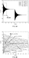
- FIG 2 depicts modelled resonance spectra of a cantilever 1 having a stiffness of 40 N/m and a resonance mode at a frequency at 300 kHz used in an embodiment of the scan head 100 according to the invention, e.g. as in FIG 1 .
- the top spectrum shows the determined amplitude for this cantilever that driven electrostatically over a range of frequencies ranging between approx. 160 and 360 kHz.
- the bottom spectrum shows the corresponding phase response.
- the response is plotted for a system in which the resistance R of the first resistor 6 is varied over a range from zero to 10 GQ. The direction of the arrow indicates increasing resistance of the first resistor. From FIG 2 (top) it can be observed that resonance amplitude of the cantilever increases with decreasing resistance.
- the resonance peak broadens indicative of a decreased Q factor, e.g. improved damping.
- the resonance frequency remain close to the initial resonance frequency f0 at 300 kHz.
- the resonance of the cantilever 1 shifts to lower frequencies f1 due to spring softening and the damping effect is gradually reduced.
- the cantilever 1 may be driven with near critical damping.
- Improving the damping of the cantilever 1 will reduce the Q-factor, e.g. increase the cantilever bandwidth.
- Increasing the cantilever bandwidth may dampen unwanted oscillations in a cantilever 1, for example resulting from step-wise changes in interaction forces between the surface of a sample 30 and a cantilever 1 comprising a probe tip 7 probing said surface.
- Improved damping may enable faster scanning, e.g. faster probing, of the surface of a sample to be probed.
- cantilever bandwidth varies between cantilevers 1, for example between cantilevers 1 having differing stiffness. Therefore, in another or further preferred embodiment the resistance of the resistor 6 is preferably adjustable.
- the first resistor 6 preferably is a tunable resistor 6, preferably within a range from 1 MQ and 10 MQ, more preferably in a range between 100k ⁇ to 100M ⁇ , even more preferably in a range between 10k ⁇ to 1G ⁇ , most preferably in a range between 1k ⁇ to 10G ⁇ .
- the resistance may be adjusted according to the properties, e.g. stiffness and/or dimension, of the cantilever 1 to be used.
- the first resistor 6 may be a switchable resistor 6 comprising an array of selectable and/or tunable resistors 6.
- the capacitance of the capacitor formed across a gap between the first electrode 2 and the second electrode formed by the cantilever 1 is such that the influence of parasitic capacitances in the system may be neglected. Therefore, the first 2 and second electrode are preferably positioned such that a capacitor with a relatively large capacitance is formed. Since the area facing the first electrode 2 for commercial cantilevers 1 is typically flat, and since capacitance at a given separation distance scales with overlap area, the surface of the first electrode 2 is preferably also flat such as to form a parallel plate capacitor.
- FIG 3A and B depict the oscillation amplitude of a cantilever 1 as a function of time according to an embodiment of the invention.
- the damping response of cantilever 1 having the properties according to the system discussed in Fig 2 , is illustrated following a simulated response to a step-wise actuation at times 0 and 0.8 ms.
- the damping properties e.g. the damping coefficient of the cantilever 1
- FIG 3B shows the individual responses in more detail.
- damping of a system wherein the first resistor 6 has a resistance of 4.6 k ⁇ is slow; 0.1 ms after triggering ringing with an amplitude in the order of 40% of the initial magnitude remains present.
- Increasing the resistance to exceedingly high values, e.g. to 4600 MQ results in over-damping of the cantilever 1 as can be observed in the graph.
- optimal damping may be achieved by optimizing the resistance of the first resistor 6.
- a resistance of 460 MQ leads to a fast damping of the oscillations, e.g. ringing.
- the cantilever may be operated under near-critical damping conditions NC.
- the resistance may be set within a rather broad range. Even when the resistance is set a factor 10 higher or lower, e.g. in a range between 46-4600 MQ, a large damping effect has still been observed.
- the cantilever 1 it is preferred to operate the cantilever 1 at near critical damping conditions. Operation at near critical damping conditions may be achieved by tuning the RC time of the system. This can be done by adjusting, e.g. selecting and/or tuning, the resistance of the first resistor 6. To find an optimal, or near- optimal resistance of the first resistor 6 for a given cantilever 1 a method as described in relation to FIG 2 may be followed. Such method, e.g.
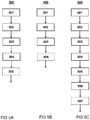
- FIG 5A comprises the steps of: providing a probe 301; driving the cantilever to oscillate 302; sweeping the drive frequency around a range a resonance frequency of the cantilever 303; measuring resonance amplitude and/or phase signal 304; optionally changing the resistance of the first resistor if needed 305; optionally, if needed, repeating the sweeping, measuring, and changing steps at least until a suitable resistance is found at which cantilever damping is a to a desired level.
- said driving is performed in a range enclosing a resonance frequency and the corresponding resonance that is shifted due to electrostatically induced spring softening.
- Said driving may be performed using known means, such as a dither piezo, or by using piezo resistively actuated cantilevers 1.
- driving the cantilever 1 may be performed electrostatically.
- a suitable the method may comprise determining a suitable starting resistance for first resistor 6. Such value may be based on previous data using obtained for similar cantilevers. Alternatively a suitable value may be calculated, or estimated, e.g. using specified or determined cantilever properties such as stiffness, resonance frequency, and/or structural cantilever properties as mass, dimension, and/or thickness. More specifically, a resistance may be chosen such that the product of series resistance and the capacitance formed by the cantilever and actuation electrode (i.e. the RC-time) is equal to 1 divided by 2n times the resonance frequency of the cantilever (i.e. 1/2 ⁇ f resonance ).
- the scan head 100 further comprises a diode 9 and second resistor 8 arranged in a (electrical) circuit parallel to the first resistor 6.
- damping may be directional depending on the orientation of the diode.
- the resistance of the second resistor 8 is smaller than the resistance of the first resistor 6 such that charge transported to and from the capacitor the via the part of the circuit comprising the diode 9 may be faster than charge transport via the part of the circuit comprising the first resistor 6.
- the diode 9 may be arranged such that a resonating cantilever 1 is only damped during a phase of the oscillation in which the cantilever approaches the surface of a sample 30 that is to be probed.
- the diode 9 may be positioned such that damping occurs during a withdrawing phase of the oscillation, e.g. during a phase of the oscillation in which the cantilever 1 moves away from the surface of a sample 30 that is to be probed.
- the second resistor 8, in accordance with the first resistor 6, may preferably be formed from a adjustable resistor and/or and array of selectable resistors.
- the capacitance may be measured.
- a cantilever 1 deflecting towards the first electrode for example induced by the tip 7 interacting with a protrusion on a sample 30 surface, will lead to a decreased separation between first 2 and second electrode, and accordingly to an increased measured capacitance.
- a probe tip 7 following a depressing the topology during the scanning of a sample 30 may lead to the cantilever 1 deflection away from the first electrode 2 as indicated by a decreased measured capacity.
- the scan head 100 comprises an electronic read-out means 10 connected to the RC circuit for determining a position of the cantilever.
- the capacitance can be measured. This may be done using e.g. an RF resonator or a single frequency 1-port S-parameter measurement system.
- the read-out circuity is de-coupled from the actuation circuitry to reduce mutual interference.
- a decoupling capacitor 18 may be provided that connects the cantilever-actuator capacitor to the read-out circuitry. It will be appreciated that other means to decouple the read-out circuity from the actuation circuitry are envisioned as well.
- the capacitance of said de-coupling capacitor 18 is comparable to the capacitance between cantilever 1 and the first electrode, e.g. actuation electrode 2.
- the first electrode e.g. actuation electrode 2
- the first electrode e.g. actuation electrode 2
- an optically transparent first electrode 2 e.g. driving electrode
- a position of the cantilever may be determined using known optical sensing methods such as optical beam deflection and interferometry.
- the present invention further or additionally relates to providing a means for reducing thermal vibrational noise by electrostatically damping.
- a means to cool the first resistor 2 to reduce thermal vibrational noise e.g. thermal cantilever vibration.
- the first 2 and second resistor may be cooled. With decreasing resistor temperature thermal noise is increasingly reduced.
- Suitable means for cooling the first and/or second resistor include but are not limited to Peltier elements and liquid nitrogen cooling.
- a method 400 for moving a probe including a conductive cantilever 1 relatively to a substrate surface 30.
- Said method comprises:
- the method preferably further comprises choosing, setting or selecting 404 the resistance of the first resistor 6 such that the characteristic RC time matches a resonance frequency of the cantilever 1 by a factor within a range from 0.1 to 10 to improve damping of cantilever oscillations, e.g. oscillations due to probing of step changes in said substrate surface 30.
- the RC time matches a resonance frequency of the cantilever 1 by a factor within 0.5 to 2, most preferably close to 1, e.g. between 0.9 and 1.1.
- Critical cantilever damping may improve cantilever response speed, such that damping is essentially within 0.02 ms or even fast e.g. within 0.01 ms, even down to 0.001 ms.
- damping cantilever oscillations e.g. within 0.02 ms, may allow operation of an imaging mode, e.g. raster scanning the probe, at a rate of around 100 lines per second using 512 sampling points per line.
- the present invention further relates to a method 500, e.g. as shown in FIG 5C , for probing the substrate surface using sub-resonant imaging with force control, e.g. analyzing the surface of a sample 30 to be measured using a sub-resonant imaging mode with force control.
- the voltage on the capacitor 1 may be used to drive the cantilever 1 away from the substrate 30. Subsequent reduction of such bias voltage may move the cantilever towards the substrate 30.
- the provided method comprises:
- said method 500 may be used to scan an area of the surface of a sample 30. Since, the cantilever 1 may be driven at, or near-to a critical damping frequency, unwanted cantilever oscillations are damped faster compared to systems providing no additional damping. In other words, cantilever ringing , e.g. resulting from generating or loosing contact between a probe tip and the sample surface is minimized, thereby allowing improving attainable scan speeds.
- the method 500 may further comprise adjusting 507 the cantilever spring constant using the electrostatic spring softening effect. This may allow setting or tuning the applied force during operation with improved accuracy.
- the scan head 100 comprises a means 12 arranged to hold the cantilever or probe chip comprising a cantilever 1 with minimal parasitic capacitance. By minimizing parasitic capacitances the cantilever can be more effectively damped. As such, it is advantageous not to use a metal mechanical clamp, e.g. to reduced the total area of unshielded conductive surfaces in the circuit.
- the scan head 100 may be provided with a vacuum chuck 12 for holding the probe chip.
- the vacuum chuck may be provided into the probe holder 11.
- the present invention relates to a probe holder 11 for holding a conductive cantilever 1 for use in a scanning probe microscope 200, the holder 11 comprising a first electrode 2 positioned such that a capacitor may be formed across a gap between the first electrode and a second electrode, e.g. upon placing a conductive cantilever 1.
- a scanning probe microscope 200 comprising the head according to the invention.
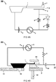
- FIG 4B schematically depicts an embodiment of a scanning probe microscope 200 according to the invention provided with a probe and a probe holder 11, along with a sample to be measured 30.
- conductive cantilever 1 comprising a probe tip 7; optically transparent second electrode 2, voltage source 4,5; first resistor 6; read-out 10 circuitry with a de-coupling capacitator; probe holder 11 comprising a vacuum chuck 12; and mechanical positioning means 13.
- a conductive cantilever 1 such that a capacitor is formed across a gap between a first electrode 2 and a second electrode, wherein the second electrode is formed by the conductive cantilever 1, and so long these provide a voltage source 4,5 for actuating the conductive cantilever 1 by applying a voltage to the capacitor; and so long these comprise at least a first resistor 6 arranged in series between the voltage source 4,5 and one of the first and second electrodes such as to form an RC circuit for damping a vibration of the cantilever 1.
- the voltage source 4,5 may be provided as a separately connectable unit.
- the first electrode may be provided on any component of an SPM system, e.g. the head 100, sample holder 11, so long a capacitor may be formed across a gap between the first electrode 2 and a conductive cantilever 1.
- the invention further relates to a scanning probe microscope 200, wherein one of the scan head 100, probe chip holder 11, or a combination there of comprises: a first electrode 2 positioned such that a capacitor is formed across a gap between the first electrode 2 and a second electrode, wherein the second electrode is formed by the conductive cantilever 1; a voltage source 4,5 for actuating the conductive cantilever 1 by applying a voltage to the capacitor; and at least a first resistor 6 arranged in series between the voltage source 4,5 and one of the first 2 and second electrodes such as to form an RC circuit for damping a vibration of the cantilever 1.
- the present invention relates to an assembly of a probe comprising a conductive cantilever 1 and a scan head 100 according to the invention.
Landscapes
- Physics & Mathematics (AREA)
- Health & Medical Sciences (AREA)
- General Health & Medical Sciences (AREA)
- General Physics & Mathematics (AREA)
- Nuclear Medicine, Radiotherapy & Molecular Imaging (AREA)
- Radiology & Medical Imaging (AREA)
- Length Measuring Devices With Unspecified Measuring Means (AREA)
Priority Applications (5)
| Application Number | Priority Date | Filing Date | Title |
|---|---|---|---|
| EP18210229.3A EP3663775A1 (de) | 2018-12-04 | 2018-12-04 | Rastersondenmikroskop, rasterkopf und verfahren |
| PCT/NL2019/050804 WO2020117056A1 (en) | 2018-12-04 | 2019-12-03 | Scanning probe microscope, scan head and method |
| KR1020217018821A KR102945489B1 (ko) | 2018-12-04 | 2019-12-03 | 스캐닝 프로브 현미경, 스캔 헤드 및 방법 |
| EP19818289.1A EP3891514B1 (de) | 2018-12-04 | 2019-12-03 | Rastersondenmikroskop, rasterkopf und verfahren |
| US17/299,431 US11592460B2 (en) | 2018-12-04 | 2019-12-03 | Scanning probe microscope, scan head and method |
Applications Claiming Priority (1)
| Application Number | Priority Date | Filing Date | Title |
|---|---|---|---|
| EP18210229.3A EP3663775A1 (de) | 2018-12-04 | 2018-12-04 | Rastersondenmikroskop, rasterkopf und verfahren |
Publications (1)
| Publication Number | Publication Date |
|---|---|
| EP3663775A1 true EP3663775A1 (de) | 2020-06-10 |
Family
ID=64606766
Family Applications (2)
| Application Number | Title | Priority Date | Filing Date |
|---|---|---|---|
| EP18210229.3A Withdrawn EP3663775A1 (de) | 2018-12-04 | 2018-12-04 | Rastersondenmikroskop, rasterkopf und verfahren |
| EP19818289.1A Active EP3891514B1 (de) | 2018-12-04 | 2019-12-03 | Rastersondenmikroskop, rasterkopf und verfahren |
Family Applications After (1)
| Application Number | Title | Priority Date | Filing Date |
|---|---|---|---|
| EP19818289.1A Active EP3891514B1 (de) | 2018-12-04 | 2019-12-03 | Rastersondenmikroskop, rasterkopf und verfahren |
Country Status (4)
| Country | Link |
|---|---|
| US (1) | US11592460B2 (de) |
| EP (2) | EP3663775A1 (de) |
| KR (1) | KR102945489B1 (de) |
| WO (1) | WO2020117056A1 (de) |
Citations (3)
| Publication number | Priority date | Publication date | Assignee | Title |
|---|---|---|---|---|
| WO2012064193A1 (en) * | 2010-11-12 | 2012-05-18 | Technische Universiteit Delft | Method for determining a spring constant for a deformable scanning probe microscope element, and scanning probe microscope and calibration device arranged for determining a spring constant for a probe element |
| US8769710B2 (en) | 2012-11-13 | 2014-07-01 | Agilent Technologies, Inc. | Atomic force microscope system using selective active damping |
| US9869695B1 (en) * | 2016-08-26 | 2018-01-16 | International Business Machines Corporation | Atomic-force microscope system with integrated fabry-perot resonator |
Family Cites Families (7)
| Publication number | Priority date | Publication date | Assignee | Title |
|---|---|---|---|---|
| EP0459723B1 (de) * | 1990-05-30 | 1996-01-17 | Hitachi, Ltd. | Halbleiterbeschleunigungsmesser und Kraftfahrzeugsteuerungssystem mit einem solchen |
| US20080315092A1 (en) * | 1994-07-28 | 2008-12-25 | General Nanotechnology Llc | Scanning probe microscopy inspection and modification system |
| US7637149B2 (en) | 2005-06-17 | 2009-12-29 | Georgia Tech Research Corporation | Integrated displacement sensors for probe microscopy and force spectroscopy |
| US7552625B2 (en) | 2005-06-17 | 2009-06-30 | Georgia Tech Research Corporation | Force sensing integrated readout and active tip based probe microscope systems |
| US7441447B2 (en) | 2005-10-07 | 2008-10-28 | Georgia Tech Research Corporation | Methods of imaging in probe microscopy |
| US7395698B2 (en) | 2005-10-25 | 2008-07-08 | Georgia Institute Of Technology | Three-dimensional nanoscale metrology using FIRAT probe |
| DE102017221076B4 (de) | 2017-11-24 | 2023-03-09 | Infineon Technologies Ag | Infrarotstrahlungssensoren |
-
2018
- 2018-12-04 EP EP18210229.3A patent/EP3663775A1/de not_active Withdrawn
-
2019
- 2019-12-03 WO PCT/NL2019/050804 patent/WO2020117056A1/en not_active Ceased
- 2019-12-03 EP EP19818289.1A patent/EP3891514B1/de active Active
- 2019-12-03 US US17/299,431 patent/US11592460B2/en active Active
- 2019-12-03 KR KR1020217018821A patent/KR102945489B1/ko active Active
Patent Citations (3)
| Publication number | Priority date | Publication date | Assignee | Title |
|---|---|---|---|---|
| WO2012064193A1 (en) * | 2010-11-12 | 2012-05-18 | Technische Universiteit Delft | Method for determining a spring constant for a deformable scanning probe microscope element, and scanning probe microscope and calibration device arranged for determining a spring constant for a probe element |
| US8769710B2 (en) | 2012-11-13 | 2014-07-01 | Agilent Technologies, Inc. | Atomic force microscope system using selective active damping |
| US9869695B1 (en) * | 2016-08-26 | 2018-01-16 | International Business Machines Corporation | Atomic-force microscope system with integrated fabry-perot resonator |
Non-Patent Citations (2)
| Title |
|---|
| BRUGGER J ET AL: "Microlever with combined integrated sensor/actuator functions for scanning force microscopy", SENSORS AND ACTUATORS A: PHYSICAL, ELSEVIER BV, NL, vol. 43, no. 1-3, 1 May 1994 (1994-05-01), pages 339 - 345, XP026615755, ISSN: 0924-4247, [retrieved on 19940501], DOI: 10.1016/0924-4247(93)00701-5 * |
| LONG CHRISTIAN J ET AL: "Modular apparatus for electrostatic actuation of common atomic force microscope cantilevers", REVIEW OF SCIENTIFIC INSTRUMENTS, AIP, MELVILLE, NY, US, vol. 86, no. 7, 1 January 1901 (1901-01-01), XP012199301, ISSN: 0034-6748, [retrieved on 19010101], DOI: 10.1063/1.4926431 * |
Also Published As
| Publication number | Publication date |
|---|---|
| US20220057430A1 (en) | 2022-02-24 |
| KR20210108375A (ko) | 2021-09-02 |
| US11592460B2 (en) | 2023-02-28 |
| KR102945489B1 (ko) | 2026-03-30 |
| EP3891514B1 (de) | 2025-10-08 |
| WO2020117056A1 (en) | 2020-06-11 |
| EP3891514A1 (de) | 2021-10-13 |
Similar Documents
| Publication | Publication Date | Title |
|---|---|---|
| McClelland et al. | Atomic force microscopy: General principles and a new implementation | |
| US7055378B2 (en) | System for wide frequency dynamic nanomechanical analysis | |
| Rabe et al. | Vibrations of free and surface‐coupled atomic force microscope cantilevers: Theory and experiment | |
| US7137291B2 (en) | Multi-dimensional force sensing for scanning probe microscopy using carbon nanotube tips and carbon nanotube oscillators | |
| US5262643A (en) | Automatic tip approach method and apparatus for scanning probe microscope | |
| US7044007B2 (en) | Force scanning probe microscope | |
| KR100540027B1 (ko) | 원자간측정방법 | |
| US20080092659A1 (en) | Whispering gallery mode ultrasonically coupled scanning probe microscopy | |
| JPH0830708B2 (ja) | 原子間力顕微鏡 | |
| JP4190936B2 (ja) | 走査型プローブ顕微鏡およびその操作法 | |
| US9921242B2 (en) | Automated atomic force microscope and the operation thereof | |
| Disseldorp et al. | MEMS-based high speed scanning probe microscopy | |
| EP3891514B1 (de) | Rastersondenmikroskop, rasterkopf und verfahren | |
| US7509844B2 (en) | Atomic force microscope technique for minimal tip damage | |
| US11668729B2 (en) | Atomic force microscope | |
| US20060156798A1 (en) | Carbon nanotube excitation system | |
| KR20180041729A (ko) | 이미징 중에 동적 모드 원자력 현미경의 상호 작용힘의 결정 | |
| CN102575975A (zh) | 利用扫描探针显微镜的材料表面的无磨损操作 | |
| Harb et al. | Resonator-based touch-sensitive probe | |
| WO2000046569A1 (en) | System and method of multi-dimensional force sensing for atomic force microscopy | |
| US20240118310A1 (en) | Device for measuring and/or modifying a surface | |
| JPH09264897A (ja) | 走査型プローブ顕微鏡 | |
| JPH1010140A (ja) | 走査型プローブ顕微鏡 | |
| JPH09119938A (ja) | 走査型プローブ顕微鏡 | |
| Maroufi et al. | Design and control of a single-chip SOI-MEMS atomic force microscope |
Legal Events
| Date | Code | Title | Description |
|---|---|---|---|
| PUAI | Public reference made under article 153(3) epc to a published international application that has entered the european phase |
Free format text: ORIGINAL CODE: 0009012 |
|
| STAA | Information on the status of an ep patent application or granted ep patent |
Free format text: STATUS: THE APPLICATION HAS BEEN PUBLISHED |
|
| AK | Designated contracting states |
Kind code of ref document: A1 Designated state(s): AL AT BE BG CH CY CZ DE DK EE ES FI FR GB GR HR HU IE IS IT LI LT LU LV MC MK MT NL NO PL PT RO RS SE SI SK SM TR |
|
| AX | Request for extension of the european patent |
Extension state: BA ME |
|
| STAA | Information on the status of an ep patent application or granted ep patent |
Free format text: STATUS: THE APPLICATION IS DEEMED TO BE WITHDRAWN |
|
| 18D | Application deemed to be withdrawn |
Effective date: 20201211 |