EP3663843A1 - Dispositif électroluminescent et afficheur au moyen dudit dispositif - Google Patents
Dispositif électroluminescent et afficheur au moyen dudit dispositif Download PDFInfo
- Publication number
- EP3663843A1 EP3663843A1 EP20153718.0A EP20153718A EP3663843A1 EP 3663843 A1 EP3663843 A1 EP 3663843A1 EP 20153718 A EP20153718 A EP 20153718A EP 3663843 A1 EP3663843 A1 EP 3663843A1
- Authority
- EP
- European Patent Office
- Prior art keywords
- light
- light emitting
- phosphor
- phosphor members
- yellow phosphor
- Prior art date
- Legal status (The legal status is an assumption and is not a legal conclusion. Google has not performed a legal analysis and makes no representation as to the accuracy of the status listed.)
- Granted
Links
Images












Classifications
-
- G—PHYSICS
- G02—OPTICS
- G02F—OPTICAL DEVICES OR ARRANGEMENTS FOR THE CONTROL OF LIGHT BY MODIFICATION OF THE OPTICAL PROPERTIES OF THE MEDIA OF THE ELEMENTS INVOLVED THEREIN; NON-LINEAR OPTICS; FREQUENCY-CHANGING OF LIGHT; OPTICAL LOGIC ELEMENTS; OPTICAL ANALOGUE/DIGITAL CONVERTERS
- G02F1/00—Devices or arrangements for the control of the intensity, colour, phase, polarisation or direction of light arriving from an independent light source, e.g. switching, gating or modulating; Non-linear optics
- G02F1/01—Devices or arrangements for the control of the intensity, colour, phase, polarisation or direction of light arriving from an independent light source, e.g. switching, gating or modulating; Non-linear optics for the control of the intensity, phase, polarisation or colour
- G02F1/13—Devices or arrangements for the control of the intensity, colour, phase, polarisation or direction of light arriving from an independent light source, e.g. switching, gating or modulating; Non-linear optics for the control of the intensity, phase, polarisation or colour based on liquid crystals, e.g. single liquid crystal display cells
- G02F1/133—Constructional arrangements; Operation of liquid crystal cells; Circuit arrangements
- G02F1/1333—Constructional arrangements; Manufacturing methods
- G02F1/1335—Structural association of cells with optical devices, e.g. polarisers or reflectors
- G02F1/1336—Illuminating devices
- G02F1/133602—Direct backlight
- G02F1/133603—Direct backlight with LEDs
-
- F—MECHANICAL ENGINEERING; LIGHTING; HEATING; WEAPONS; BLASTING
- F21—LIGHTING
- F21K—NON-ELECTRIC LIGHT SOURCES USING LUMINESCENCE; LIGHT SOURCES USING ELECTROCHEMILUMINESCENCE; LIGHT SOURCES USING CHARGES OF COMBUSTIBLE MATERIAL; LIGHT SOURCES USING SEMICONDUCTOR DEVICES AS LIGHT-GENERATING ELEMENTS; LIGHT SOURCES NOT OTHERWISE PROVIDED FOR
- F21K9/00—Light sources using semiconductor devices as light-generating elements, e.g. using light-emitting diodes [LED] or lasers
- F21K9/60—Optical arrangements integrated in the light source, e.g. for improving the colour rendering index or the light extraction
- F21K9/64—Optical arrangements integrated in the light source, e.g. for improving the colour rendering index or the light extraction using wavelength conversion means distinct or spaced from the light-generating element, e.g. a remote phosphor layer
-
- G—PHYSICS
- G02—OPTICS
- G02F—OPTICAL DEVICES OR ARRANGEMENTS FOR THE CONTROL OF LIGHT BY MODIFICATION OF THE OPTICAL PROPERTIES OF THE MEDIA OF THE ELEMENTS INVOLVED THEREIN; NON-LINEAR OPTICS; FREQUENCY-CHANGING OF LIGHT; OPTICAL LOGIC ELEMENTS; OPTICAL ANALOGUE/DIGITAL CONVERTERS
- G02F1/00—Devices or arrangements for the control of the intensity, colour, phase, polarisation or direction of light arriving from an independent light source, e.g. switching, gating or modulating; Non-linear optics
- G02F1/01—Devices or arrangements for the control of the intensity, colour, phase, polarisation or direction of light arriving from an independent light source, e.g. switching, gating or modulating; Non-linear optics for the control of the intensity, phase, polarisation or colour
- G02F1/13—Devices or arrangements for the control of the intensity, colour, phase, polarisation or direction of light arriving from an independent light source, e.g. switching, gating or modulating; Non-linear optics for the control of the intensity, phase, polarisation or colour based on liquid crystals, e.g. single liquid crystal display cells
- G02F1/133—Constructional arrangements; Operation of liquid crystal cells; Circuit arrangements
- G02F1/1333—Constructional arrangements; Manufacturing methods
- G02F1/1335—Structural association of cells with optical devices, e.g. polarisers or reflectors
- G02F1/1336—Illuminating devices
- G02F1/133602—Direct backlight
- G02F1/133606—Direct backlight including a specially adapted diffusing, scattering or light controlling members
-
- G—PHYSICS
- G02—OPTICS
- G02F—OPTICAL DEVICES OR ARRANGEMENTS FOR THE CONTROL OF LIGHT BY MODIFICATION OF THE OPTICAL PROPERTIES OF THE MEDIA OF THE ELEMENTS INVOLVED THEREIN; NON-LINEAR OPTICS; FREQUENCY-CHANGING OF LIGHT; OPTICAL LOGIC ELEMENTS; OPTICAL ANALOGUE/DIGITAL CONVERTERS
- G02F1/00—Devices or arrangements for the control of the intensity, colour, phase, polarisation or direction of light arriving from an independent light source, e.g. switching, gating or modulating; Non-linear optics
- G02F1/01—Devices or arrangements for the control of the intensity, colour, phase, polarisation or direction of light arriving from an independent light source, e.g. switching, gating or modulating; Non-linear optics for the control of the intensity, phase, polarisation or colour
- G02F1/13—Devices or arrangements for the control of the intensity, colour, phase, polarisation or direction of light arriving from an independent light source, e.g. switching, gating or modulating; Non-linear optics for the control of the intensity, phase, polarisation or colour based on liquid crystals, e.g. single liquid crystal display cells
- G02F1/133—Constructional arrangements; Operation of liquid crystal cells; Circuit arrangements
- G02F1/1333—Constructional arrangements; Manufacturing methods
- G02F1/1335—Structural association of cells with optical devices, e.g. polarisers or reflectors
- G02F1/1336—Illuminating devices
- G02F1/133602—Direct backlight
- G02F1/133609—Direct backlight including means for improving the color mixing, e.g. white
-
- F—MECHANICAL ENGINEERING; LIGHTING; HEATING; WEAPONS; BLASTING
- F21—LIGHTING
- F21Y—INDEXING SCHEME ASSOCIATED WITH SUBCLASSES F21K, F21L, F21S and F21V, RELATING TO THE FORM OR THE KIND OF THE LIGHT SOURCES OR OF THE COLOUR OF THE LIGHT EMITTED
- F21Y2115/00—Light-generating elements of semiconductor light sources
- F21Y2115/10—Light-emitting diodes [LED]
-
- G—PHYSICS
- G02—OPTICS
- G02F—OPTICAL DEVICES OR ARRANGEMENTS FOR THE CONTROL OF LIGHT BY MODIFICATION OF THE OPTICAL PROPERTIES OF THE MEDIA OF THE ELEMENTS INVOLVED THEREIN; NON-LINEAR OPTICS; FREQUENCY-CHANGING OF LIGHT; OPTICAL LOGIC ELEMENTS; OPTICAL ANALOGUE/DIGITAL CONVERTERS
- G02F1/00—Devices or arrangements for the control of the intensity, colour, phase, polarisation or direction of light arriving from an independent light source, e.g. switching, gating or modulating; Non-linear optics
- G02F1/01—Devices or arrangements for the control of the intensity, colour, phase, polarisation or direction of light arriving from an independent light source, e.g. switching, gating or modulating; Non-linear optics for the control of the intensity, phase, polarisation or colour
- G02F1/13—Devices or arrangements for the control of the intensity, colour, phase, polarisation or direction of light arriving from an independent light source, e.g. switching, gating or modulating; Non-linear optics for the control of the intensity, phase, polarisation or colour based on liquid crystals, e.g. single liquid crystal display cells
- G02F1/133—Constructional arrangements; Operation of liquid crystal cells; Circuit arrangements
- G02F1/1333—Constructional arrangements; Manufacturing methods
- G02F1/1335—Structural association of cells with optical devices, e.g. polarisers or reflectors
- G02F1/1336—Illuminating devices
- G02F1/133614—Illuminating devices using photoluminescence, e.g. phosphors illuminated by UV or blue light
-
- H—ELECTRICITY
- H10—SEMICONDUCTOR DEVICES; ELECTRIC SOLID-STATE DEVICES NOT OTHERWISE PROVIDED FOR
- H10W—GENERIC PACKAGES, INTERCONNECTIONS, CONNECTORS OR OTHER CONSTRUCTIONAL DETAILS OF DEVICES COVERED BY CLASS H10
- H10W72/00—Interconnections or connectors in packages
- H10W72/20—Bump connectors, e.g. solder bumps or copper pillars; Dummy bumps; Thermal bumps
- H10W72/221—Structures or relative sizes
- H10W72/227—Multiple bumps having different sizes
-
- H—ELECTRICITY
- H10—SEMICONDUCTOR DEVICES; ELECTRIC SOLID-STATE DEVICES NOT OTHERWISE PROVIDED FOR
- H10W—GENERIC PACKAGES, INTERCONNECTIONS, CONNECTORS OR OTHER CONSTRUCTIONAL DETAILS OF DEVICES COVERED BY CLASS H10
- H10W90/00—Package configurations
- H10W90/701—Package configurations characterised by the relative positions of pads or connectors relative to package parts
- H10W90/721—Package configurations characterised by the relative positions of pads or connectors relative to package parts of bump connectors
- H10W90/724—Package configurations characterised by the relative positions of pads or connectors relative to package parts of bump connectors between a chip and a stacked insulating package substrate, interposer or RDL
Definitions
- a white light emitting device includes a circuit board; a plurality of light sources mounted on the circuit board, each light source of the plurality of light sources configured to emit monochromatic light; a light converter spaced apart from the circuit board, the light converter configured to convert the monochromatic light emitted from the light sources to white light; and a compensator provided between the circuit board and the light converter, the compensator configured to convert the emitted monochromatic light to white light.
- the compensator may include a plurality of phosphor members having a yellow phosphor.
- the plurality of phosphor members may include a first group of phosphor members disposed on an edge of the circuit board, and a second group of phosphor members disposed at a center of the circuit board, and the first group may be more densely arranged than the second group.
- FIG. 1 is a schematic exploded perspective view of a white light emitting device in accordance with one exemplary embodiment.
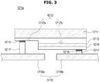
- the light emitting device 121a may have a structure in which a substrate 1211, an N-type semiconductor layer 1212, an active layer 1213, and a P-type semiconductor layer 1214 are sequentially stacked.
- the active layer 1213 may be formed with an InGaN/GaN layer having a multi-quantum well structure.
- the body 121b accommodates the light emitting device 121a.
- the body 121b may be formed of at least one from among a resin based material such as polyphthalamide (PPA), silicon (Si), aluminum (Al), aluminum nitride (AIN), a liquid crystal polymer (PSG, photo sensitive glass), a polyamide9T (PA9T), a syndiotactic polystyrene (SPS), a metal material, sapphire (Al2O3), beryllium oxide (BeO), and a printed circuit board (PCB) 110, but it is not limited thereto.
- a resin based material such as polyphthalamide (PPA), silicon (Si), aluminum (Al), aluminum nitride (AIN), a liquid crystal polymer (PSG, photo sensitive glass), a polyamide9T (PA9T), a syndiotactic polystyrene (SPS), a metal material, sapphire (Al2O3), beryllium oxide
- the cavity 123 may be formed in a shape in which the width of the cavity 123 decreases in a downward direction. That is, a sidewall 124 of the cavity 123 may be formed to be sloped.
- a reflection angle of the monochromatic light emitted by the light emitting device 121a varies according to an angle of the sidewall 124. Therefore, the degree of slope of the sidewall 124 may be adjusted to adjust a beam angle of the monochromatic light.
- a reflective material which reflects light generated by the light emitting device 121a may be coated on the sidewall 124 and a use rate of light generated by the light emitting device 121a may be increased.
- the phosphor may include at least one of a variety of light emitting material among a yttrium aluminum garnet (YAG) based material, a terbium aluminum garnet (TAG) based material, a silicate based material, a sulfide based material, a nitride based material, a borate based material, and a phosphate based material
- YAG yttrium aluminum garnet
- TAG terbium aluminum garnet
- silicate based material a silicate based material
- sulfide based material a sulfide based material
- nitride based material a nitride based material
- borate based material a borate based material
- phosphate based material the light emitting material configuring the phosphor is not limited thereto.
- the light converter 130 may include a yellow light emitting phosphor having a complementary color of a blue color.
- the yellow light emitting phosphor includes a YAG based light emitting material, absorbs incident blue light, and emits yellow light. Then, blue light not involved in light emitting of the yellow color phosphor and yellow light emitted by the yellow color phosphor are mixed to become white light.
- the light converter 130 when the light source 120 emits red light, the light converter 130 may include a cyan light emitting phosphor having a complementary color of the red color, and when the light source 120 emits green light, the light converter 130 may include a magenta light emitting phosphor having a complementary color of the green color.
- the light converter 130 may include a plurality of phosphors which emit different colors from each other. That is, the light converter 130 may generate complementary color light having a complementary color of the monochromatic light emitted by the light source 120 using the plurality of phosphors.
- the compensator 140 converts part of light incident to the light converter 130 through a different light path to white light to reduce the color mura.
- the compensator 140 may include at least one phosphor member 141 which converts an incident monochromatic light to white light.
- the phosphor member 141 may include a yellow light emitting phosphor, incident blue light is converted to white light, and because the light converter 130 may include a red light emitting phosphor and green light emitting phosphor, incident blue light is converted to white light.
- the compensator 140 may be provided adjacent the circuit board 110, and convert monochromatic light ML reflected by the circuit board 110 to white light.
- the reflector 150 may be provided in a reflective sheet or reflective film shape and be coupled to the circuit board 110 by bonding to the circuit board 110 on which a compensator 140 is provided, a method of forming the reflector 150 is not limited thereto.
- the reflector 150 may be formed by a method of depositing a reflective member on the circuit board 110 on which the compensator 140 is provided, or printing or coating the reflective member mixed with the adhesive onto the circuit board 110 on which the compensator 140 is provided by mixing a reflective member with an adhesive.
- a compensator 140 is formed on a reflective sheet or reflective film, and the reflective sheet or the reflective film may be coupled to a circuit board 110 to form a lower part of a white light emitting device 100.
- shapes of phosphor members 141 and an arrangement pattern of phosphor members 141 may be described in detail.
- the area of the phosphor member 141 per unit light source may be determined according to a size of the phosphor member 141 and the number of phosphor members 141. That is, when n phosphor members 141 having a size A per the light source 120 are disposed, the area of the phosphor members 141 per the light source is A ⁇ n.
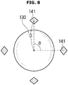
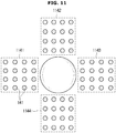
- the phosphor members 141 may be arranged in a regular pattern included in a space between a light source 120 and another light source 120. Specifically, as shown in FIGS. 7 to 10 , the plurality of phosphor members 141 may be provided at a predetermined distance (D) from the light source 120, and each phosphor member 141 may be arranged to have an interval having a predetermined angle ( ⁇ ) around the light source 120.
- D predetermined distance
- ⁇ predetermined angle
- the number of the phosphor members 141 and the size of each phosphor member 141 configuring each of the groups 1141, 1142, 1143, and 1144 may be determined according to a level of a color mura as described above.
- the arrangement pattern of the phosphor members 141 on the edge of the white light emitting device 100 may be different from the other portions.
- FIG. 13 is a view for describing an arrangement pattern of phosphor members on an edge of the white light emitting device 100 in accordance with one exemplary embodiment.
- phosphor members 141a corresponding to a light source 120a located on an edge of a white light emitting device 100 and phosphor members 141b corresponding to a light source 120b located on a center of the white light emitting device 100 have different sizes.
- the size of the phosphor member 141a corresponding to the light source 120a located on the edge may be greater than that of the phosphor member 141b corresponding to the light source 120b located on the center so that a color mura is further compensated on the edge where the color mura is comparatively severely generated.
- the phosphor members 141d corresponding to the light source 120d located on the center of the white light emitting device 100 may be a circular shape, and the phosphor members 141c corresponding to a light source 120c located on the edge may be polygonal shape so that a color mura is further compensated on the edge where the color mura is comparatively severely generated.
- the phosphor members 141 are located between the light source 120 and another light source 120 in FIG. 1 to 14 , the dispositions of the phosphor members 141 are not limited thereto. Hereinafter, arrangement positions of the phosphor members 141 will be described.
- FIG. 15 is a cross-sectional view for describing an arrangement position change of phosphor members of a white light emitting device in accordance with one exemplary embodiment.
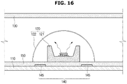
- FIG. 16 is a cross-sectional view for describing an arrangement position change of phosphor members of a white light emitting device in accordance with another exemplary embodiment.
- FIG. 17 is a cross-sectional view for describing an arrangement position change of phosphor members of a white light emitting device in accordance with still another exemplary embodiment.
- phosphor members 145 provided inside a light source 120 may convert a monochromatic light refracted and reflected inside of the light source 120 to white light.
- the phosphor members 145 may be disposed between a light emitting device package 121 and a lens 122.
- FIG. 18 is a plan view of a light source for describing an arrangement pattern of phosphor members according to yet another exemplary embodiment.
- FIG. 19 is a plan view of a light source for describing an arrangement pattern of phosphor members according to yet another exemplary embodiment.
- FIG. 20 is a plan view of a light source for describing an arrangement pattern of phosphor members according to yet another exemplary embodiment.
- a light emitting device package 121 is provided inside a lens 122.
- the lens 122 may be fixed on a circuit board 110 by a supporter 127 disposed in an angle of 120 degrees.
- Phosphor members 145 are provided in a space between the lens 122 and the light emitting device package 121. As shown in FIG. 18 to 20 , the phosphor members 145 may be arranged in spaces between supporters 127.
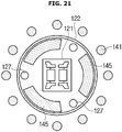
- FIG. 21 is a view for describing an arrangement pattern of phosphor members according to yet another exemplary embodiment.
- a compensator may include first phosphor members 141 provided between the light source 120 and another light source, and second phosphor members 145 existing inside the light source 120.
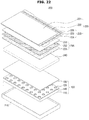
- FIG. 22 is an exploded perspective view of a display device in accordance with one exemplary embodiment.
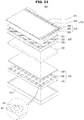
- FIG. 23 is an exploded perspective view of a display device in accordance with another exemplary embodiment.
- the frame 210 accommodates the liquid crystal panel 220, the optical part 235, and the white light emitting device 100.
- the frame 210 may have a square frame shape, and may be formed of a plastic or reinforced plastic.
- a chassis which surrounds the frame 210 and supports a backlight assembly may be disposed under or on sides of the frame 210 to improve the durability and the fire resistance of the frame 210.
- liquid crystal panel 220 In addition to the liquid crystal panel 220 described above, various panels which may be considered by those skilled in the art may be one exemplary embodiment of the liquid crystal panels 220.
- a touch panel which includes a polyester film, glass, and the like may be installed to sense a touch operation or a polaroid film may be further installed to polarize light transmitted to the outside through the liquid crystal panel 220.
- the optical part 235 may include a diffusion sheet 233 and prism sheets 231 and 232.
- the diffusion sheet 233 serves to diffuse light emitted by the diffusion plate 240, and the prism sheets 231 and 232 serve to collect the light diffused by the diffusion sheet 233 to supply the uniform light to the liquid crystal panel 220.
- the diffusion sheet 233 diffuses and outputs incident light. Further uniform white light may be provided to the liquid crystal panel 220 by the diffusion sheet 233.
- the diffusion sheet 233 may be omitted or configured with a plurality of sheets as desired.
- the prism sheets 231 and 232 may include a first prism sheet 231 and a second prism sheet 232 in which prisms vertically intersect in x and y axes directions.
- the prism sheets 231 and 232 refract light from x and y axes directions, the linearity of the light may be improved.
- the white light emitting device 100 described above may be applied to a display device 200.
- the white light emitting device 100 may provide a backlight to the liquid crystal panel 220 described above.
- the light sources 120 may be provided in a package type and the plurality of light sources 120 may be mounted on the circuit board 110.
- the light sources 120 are arranged in a lattice pattern, an arrangement pattern of the light sources may be changed in various shapes as desired.
- the light source 120 generates and emits a monochromatic light.
- the light source 120 may emit blue light generated by a blue LED.
- blue light generated by a blue LED may be emitted in a wide beam angle through the lens (122 of FIG. 2 ) described above.
- the light converter 130 may include a phosphor.
- the light converter 130 may include a yellow light emitting phosphor having a complementary color of blue light.
- the light converter 130 may include a light phosphor and a green light emitting phosphor instead of a yellow light emitting phosphor to generate white light.
- White light transmitted by the light converter 130 reaches the liquid crystal panel 220 passing through the diffusion plate 240 and the optical part 235. Therefore, the liquid crystal panel 220 uses white light provided by the white light emitting device 100 as a backlight to display a predetermined image.
- the refraction, reflection, and diffraction of light may occur inside the display device 200 and the white light emitting device 100. Therefore, a color mura may occur in white light emitted by the white light emitting device 100 according to a change of a light path.
- the compensator 140 may be located between the circuit board 110 and the light converter 130, and convert a monochromatic light, which is refracted, reflected, and rotated, to white light to compensate the color mura.
- the phosphor included in the phosphor member 141 may be the same as the phosphor of the light converter 130 described above.
- the phosphor members 141 may include a yellow light emitting phosphor having a complementary color of blue light.
- the phosphor members 141 may include a light phosphor and a green light emitting phosphor instead of a yellow light emitting phosphor to generate white light.
- the phosphor members 141 may be provided between the light source 120 and the light source 120, but also provided inside the light source 120. In addition, the phosphor members 141 may be provided both inside and between the light sources 120.
- a shape and a size of the respective phosphor members 141 may be determined according to the level of the color mura, and the compensator 140 may include the plurality of phosphor members 141 having different shapes.
- the compensator 140 may be provided in a compensation sheet shape or a compensation film shape including the phosphor members 141, and be formed by bonding the compensation sheet or the compensation film to the circuit board 110.
- the compensator 140 may be formed by a method of directly printing the phosphor member 141 on the circuit board 110.
- the compensator 140 may be formed by a method of mixing a phosphor with an adhesive configured to fix the phosphor to the circuit board 110 in order to form a phosphor ink, and directly printing the phosphor ink formed on the circuit board 110 to form the phosphor members 141.
- a compensator 140 may be directly formed on a reflective sheet or film.
- the compensator 140 may be formed by a method of coating phosphor members 141 in a regular pattern onto the reflective sheet or the reflective film, or a method of depositing the phosphor members 141 in a regular pattern on the reflective sheet or the reflective film.
- the compensator 140 may be formed by a method of directly printing the phosphor members 141 on the reflective sheet or the reflective film.
- the compensator 140 may be formed by a method of mixing a phosphor with an adhesive configured to fix the phosphor to the reflective sheet or the reflective film to form a phosphor ink, and directly printing the phosphor ink formed on the reflective sheet or the reflective film to form the phosphor members 141.
- the phosphor members 141 may be formed in a regular pattern.
- FIG. 24 is a schematic exploded perspective view of a white light emitting device including a plurality of light source modules
- FIG. 25 is a schematic perspective view for describing a light source module
- FIG. 26 is a cross-sectional view of a white light emitting device
- FIG. 27 is a cross-sectional view of a white light emitting device which further includes a coated layer.
- a white light emitting device includes a base, a plurality of light source modules 320 emitting a monochromatic light, and a light converter 130 converting the monochromatic light emitted from the plurality of light source modules 320 to white light.
- the base 310 may be omitted as desired, or be replaced with a different component.
- the frame 210 illustrated in FIG. 22 may become the base 310. That is, the plurality of light source modules 320 may be coupled to the frame 210.
- the light converter 130 converts a monochromatic light to white light.
- the light converter 130 is spaced a certain distance from the light source module 320, converts a monochromatic light emitted from the light source module 320 to white light, and emits the white light forward.
- the light converter 130 may include a phosphor which converts a wavelength of an incident monochromatic light and emits a monochromatic light having a different color.
- the plurality of light source modules 320 may be spaced a certain distance D1 from each other. At this time, distances between the light source modules 320 may be the same, but the distances between the light source modules 320 may be different from each other when it is required. For example, a distance between a second light source module 320-2 and a third light source module 320-3 may be smaller than that of a first light source module 320-1 and the second light source module 320-2, but it is not limited thereto.
- the light source module 320_1 includes a circuit board 110, compensators 140, and a plurality of light sources 120.
- the plurality of light sources 120 are mounted on the circuit board 110.
- the circuit board 110 may be provided in a long bar shape.
- the length L of the circuit board 110 may be determined to correspond to the length of the white light emitting device 300, the width W1 of the circuit board 110 may be determined to correspond to the width of the light source 120. Specifically, as illustrated in FIG. 25 , the width W1 of the circuit board 110 may be greater than the width W2 of the light source 120, but is not limited thereto, and may have a width in which a light emitting device package of the light source 120 may be mounted.
- the plurality of light sources 120 are mounted on the circuit board 110 with a certain interval, and emit a monochromatic light.
- the intervals between the plurality of light sources 120 may be the same, but the plurality of light sources 120 may be also disposed with the intervals different from each other.
- the compensator 140 is provided between the light converter 130 and the circuit board 110 to improve the color uniformity of the white light emitting device 300. Specifically, the compensator 140 converts an incident monochromatic light to white light and output the white light to reduce a color mura of the white light emitting device 300.
- the compensator 140 may include a plurality of phosphor members 141 which convert an incident monochromatic light to white light and output the white light.
- the phosphor member 141 may include a phosphor which is formed of at least one phosphor material and converts a wavelength of an incident monochromatic light. Phosphor material forming the phosphor member 141 may be determined according to a monochromatic light incident from the light source 120.
- the compensator 140 may be provided by a method of forming the plurality of phosphor members 141 on the circuit board 110. Specifically, the compensator 140 may be formed by a method of coating the phosphor members 141 in a regular pattern on the circuit board 110, or a method of depositing the phosphors members 141 in a regular pattern on the circuit board 110.
- the compensator 140 may be also formed by a method of directly printing the phosphor member 141 on the circuit board 110.
- the compensator 140 may be formed by a method of mixing a phosphor with an adhesive for fixing the phosphor to the circuit board 110 to form a phosphor ink, and directly printing the formed phosphor ink on the circuit board 110 to form the phosphor member 141.
- the phosphor member 141 may be provided inside or outside the light source 120, but the position of the phosphor member 141 is not limited thereto.
- the phosphor member 141 may be formed inside the light source 120 or outside the light source 120 as described above, or may be formed inside and outside the light source 120.
- the white light emitting device 300 may further include a coated layer 330 which is transparent.
- the coated layer 330 may be stacked on the circuit board 110, in which the phosphor member 141 is formed, to prevent the phosphor member 141 and the circuit board 110 from being damaged.
- FIG. 28 is an exploded perspective view of a white light emitting device which further includes a reflector
- FIG. 29 is a cross-sectional view of a white light emitting device which further includes a reflector.
- the white light emitting device 300 including the plurality of light source modules 320 may further include a reflector 340.
- the reflector 340 may be stacked on the plurality of light source modules 320, and reflect light emitted from the light source 120 toward the light converter 130 to increase a use rate of the light source 120. At this time, the reflector 340 may be provided in a reflective sheet or a reflective film type.
- the reflector 340 may be provided by a method of stacking on the light source module 320 on which the light sources 120 are mounted. To this end, the reflector 340 may include a plurality of openings formed to correspond to the plurality of light sources 120. The diameter of the openings formed in the reflector 340 may be greater than that of the light source 120.
- the color uniformity of a white light emitting device can be improved by converting a monochromatic light, which is reflected and refracted inside of the white light emitting device, to white light.
- the device according to the present disclosure may also be described as set out in the following paragraphs.
- a white light emitting device comprising: a plurality of light sources (120) which are mounted on a board (110) and which each emit a monochromatic light; a light converter (130) which is spaced apart from the board and converts the monochromatic light incident from the plurality of light sources (120) to white light; and a compensator (140) which is provided between the board and the light converter and converts the incident monochromatic light to a different wavelength.
- the compensator (140) may be formed directly on a sheet or film that is stacked on the board.
- the compensator may be formed on the light sources (120).
- the compensator (140) may include a plurality of phosphor members (141) formed of a phosphor having a color complementary to the incident monochromatic light.
- the plurality of phosphor members (141) may be disposed between the plurality of light sources (120).
- the plurality of phosphor members (141) may be disposed inside the plurality of light sources (120).
- Each of the plurality of light sources (120) may include a light emitting device package (121) which generates a monochromatic light and a lens (122) which accommodates the light emitting device package (121) and externally emits the monochromatic light.
- the phosphor members (141) may be disposed between the light emitting device package (121) and the lens (122) and convert a monochromatic light reflected inside of the light sources.
- An arrangement pattern of the plurality of phosphor members (141) may be determined according to a pattern of a color mura of the white light converted by and emitted from the light converter.
- the phosphor members (141) may be further densely disposed on an edge of the circuit board compared to a center of the circuit board.
- a size of the phosphor member (141) on an edge of the board may be greater than that on a center of the board (110).
- the white light emitting device (100) according to the present disclosure may further comprise: a coated layer stacked on the compensator.
- the white light emitting device (100) may further comprise: a reflector (150) including a plurality of openings corresponding to the plurality of light sources (120), stacked on the board (110), and reflecting the monochromatic light toward the light converter.
- a reflector (150) including a plurality of openings corresponding to the plurality of light sources (120), stacked on the board (110), and reflecting the monochromatic light toward the light converter.
- a display device comprising: a liquid crystal panel; a light guide plate provided in a rear of the liquid crystal panel; and a white light emitting device which is provided in a rear of the light guide plate, and emits white light onto the light guide plate, wherein the white light emitting device is according to the present disclosure.
- a white light emitting device comprising: a board (110); a plurality of light sources (120) mounted on the board (110), each of the plurality of light sources (120) includes a light emitting device (121a) configured to emit blue light and a lens (122); a light converter (130) spaced apart from the board (110) and configured to emit white light in response to blue light being incident on the light converter (130); and a compensator (140) provided between the a light converter (130) and a board (110), and configured to emit white light in response to blue light being incident on the compensator (140), wherein the compensator (140) includes a plurality of phosphor members (141), each of which are formed of a yellow light emitting phosphor.
- the phosphor members (141) may be arranged around the light emitting device (121a) at interval having a predetermined angle ( ⁇ ).
- the compensator (140) may be formed directly on the board (110).
- the compensator (140) may be formed directly on a sheet or film that is stacked on the board.
- At least part of the plurality of phosphor members (141) may be disposed inside of each light sources (120).
- the plurality of phosphor members (141) may be disposed between the plurality of light sources (120).
- a size of the phosphor member (141) on an edge of the board may be greater than that on a center of the board (110).
- the compensator (140) may be formed of at least one from a sheet or film.
- the phosphor members (141) may have a shape corresponding to a circle.
- the plurality of phosphor members (141) may be provided at a predetermined distance (D) from the light emitting device (121a).
Landscapes
- Physics & Mathematics (AREA)
- Nonlinear Science (AREA)
- Optics & Photonics (AREA)
- Crystallography & Structural Chemistry (AREA)
- Chemical & Material Sciences (AREA)
- General Physics & Mathematics (AREA)
- Mathematical Physics (AREA)
- Engineering & Computer Science (AREA)
- General Engineering & Computer Science (AREA)
- Microelectronics & Electronic Packaging (AREA)
- Led Device Packages (AREA)
- Planar Illumination Modules (AREA)
- Spectroscopy & Molecular Physics (AREA)
- Devices For Indicating Variable Information By Combining Individual Elements (AREA)
- Fastening Of Light Sources Or Lamp Holders (AREA)
Applications Claiming Priority (4)
| Application Number | Priority Date | Filing Date | Title |
|---|---|---|---|
| KR20140171973 | 2014-12-03 | ||
| KR1020150092852A KR102094829B1 (ko) | 2014-12-03 | 2015-06-30 | 백색 발광 장치 및 이를 이용한 디스플레이 장치 |
| EP15195259.5A EP3029515B1 (fr) | 2014-12-03 | 2015-11-18 | Dispositif électroluminescent et dispositif d'affichage utilisant ce dispositif |
| EP19153846.1A EP3499302B1 (fr) | 2014-12-03 | 2015-11-18 | Dispositif électroluminescent et afficheur au moyen dudit dispositif |
Related Parent Applications (3)
| Application Number | Title | Priority Date | Filing Date |
|---|---|---|---|
| EP19153846.1A Division EP3499302B1 (fr) | 2014-12-03 | 2015-11-18 | Dispositif électroluminescent et afficheur au moyen dudit dispositif |
| EP19153846.1A Division-Into EP3499302B1 (fr) | 2014-12-03 | 2015-11-18 | Dispositif électroluminescent et afficheur au moyen dudit dispositif |
| EP15195259.5A Division EP3029515B1 (fr) | 2014-12-03 | 2015-11-18 | Dispositif électroluminescent et dispositif d'affichage utilisant ce dispositif |
Publications (2)
| Publication Number | Publication Date |
|---|---|
| EP3663843A1 true EP3663843A1 (fr) | 2020-06-10 |
| EP3663843B1 EP3663843B1 (fr) | 2022-02-23 |
Family
ID=54608370
Family Applications (3)
| Application Number | Title | Priority Date | Filing Date |
|---|---|---|---|
| EP19153846.1A Active EP3499302B1 (fr) | 2014-12-03 | 2015-11-18 | Dispositif électroluminescent et afficheur au moyen dudit dispositif |
| EP15195259.5A Active EP3029515B1 (fr) | 2014-12-03 | 2015-11-18 | Dispositif électroluminescent et dispositif d'affichage utilisant ce dispositif |
| EP20153718.0A Active EP3663843B1 (fr) | 2014-12-03 | 2015-11-18 | Dispositif électroluminescent et afficheur au moyen dudit dispositif |
Family Applications Before (2)
| Application Number | Title | Priority Date | Filing Date |
|---|---|---|---|
| EP19153846.1A Active EP3499302B1 (fr) | 2014-12-03 | 2015-11-18 | Dispositif électroluminescent et afficheur au moyen dudit dispositif |
| EP15195259.5A Active EP3029515B1 (fr) | 2014-12-03 | 2015-11-18 | Dispositif électroluminescent et dispositif d'affichage utilisant ce dispositif |
Country Status (4)
| Country | Link |
|---|---|
| US (4) | US10545375B2 (fr) |
| EP (3) | EP3499302B1 (fr) |
| CN (1) | CN116184721B (fr) |
| WO (1) | WO2016089102A1 (fr) |
Families Citing this family (20)
| Publication number | Priority date | Publication date | Assignee | Title |
|---|---|---|---|---|
| US12000582B2 (en) | 2014-10-31 | 2024-06-04 | Lg Electronics Inc. | Display device having reflecting sheet with plurality of dot areas reducing reflectivity of the reflecting sheet |
| WO2016068590A1 (fr) * | 2014-10-31 | 2016-05-06 | Lg Electronics Inc. | Unité de rétro-éclairage et dispositif d'affichage comprenant une unité de rétro-éclairage |
| KR102367810B1 (ko) * | 2015-07-13 | 2022-02-28 | 삼성전자주식회사 | 반사판, 백 라이트 유닛 및 디스플레이 장치 |
| DE102016109519A1 (de) * | 2016-05-24 | 2017-11-30 | Osram Gmbh | Eindeckungsteil für ein Gewächshaus, Gewächshaus und Verwendung einer Schicht für ein Eindeckungsteil |
| CN208041696U (zh) * | 2018-04-16 | 2018-11-02 | 京东方科技集团股份有限公司 | 背光源、背光模组和显示装置 |
| KR102723458B1 (ko) * | 2019-04-29 | 2024-10-30 | 엘지이노텍 주식회사 | 조명 모듈 및 이를 구비한 조명 장치 |
| WO2021114526A1 (fr) * | 2019-12-13 | 2021-06-17 | 海信视像科技股份有限公司 | Dispositif d'affichage |
| CN113296309A (zh) * | 2020-02-24 | 2021-08-24 | 海信视像科技股份有限公司 | 一种显示装置 |
| US11487158B2 (en) | 2020-03-25 | 2022-11-01 | Samsung Electronics Co., Ltd. | Backlight unit, method of manufacturing the same and display apparatus including the same |
| KR102852963B1 (ko) * | 2020-03-25 | 2025-09-01 | 삼성전자주식회사 | 백라이트 유닛, 이의 제조 방법 및 이를 포함하는 디스플레이 장치 |
| KR102873277B1 (ko) | 2020-05-08 | 2025-10-20 | 삼성전자주식회사 | 발광 장치 |
| KR102793957B1 (ko) | 2020-09-16 | 2025-04-14 | 삼성전자주식회사 | 디스플레이 장치 및 그 제조 방법 |
| CN116325184A (zh) * | 2021-01-04 | 2023-06-23 | 三星电子株式会社 | 显示装置及其光源设备 |
| CN115220257A (zh) | 2021-01-05 | 2022-10-21 | 三星电子株式会社 | 显示装置以及用于显示装置的组件 |
| EP4276524A3 (fr) * | 2021-01-05 | 2023-12-13 | Samsung Electronics Co., Ltd. | Appareil d'affichage |
| WO2022149653A1 (fr) * | 2021-01-05 | 2022-07-14 | 삼성전자주식회사 | Dispositif d'affichage |
| US11333928B1 (en) | 2021-01-05 | 2022-05-17 | Samsung Electronics Co., Ltd. | Display apparatus comprising a reflective sheet having a plurality of first and second light conversion dots respectively disposed around a plurality of first and second holes |
| KR102674818B1 (ko) | 2021-05-24 | 2024-06-12 | 엘지전자 주식회사 | 디스플레이 디바이스 |
| US11561434B1 (en) * | 2021-11-02 | 2023-01-24 | Innolux Corporation | Light-emitting module and electronic device |
| TWI882499B (zh) * | 2023-10-30 | 2025-05-01 | 隆達電子股份有限公司 | 光源模組 |
Citations (2)
| Publication number | Priority date | Publication date | Assignee | Title |
|---|---|---|---|---|
| EP2363884A1 (fr) * | 2010-01-18 | 2011-09-07 | LG Innotek Co., Ltd. | Unité d'éclairage et dispositif d'affichage la comprenant |
| US20130070448A1 (en) * | 2011-09-15 | 2013-03-21 | Osram Sylvania Inc. | Led lamp |
Family Cites Families (38)
| Publication number | Priority date | Publication date | Assignee | Title |
|---|---|---|---|---|
| US6340824B1 (en) * | 1997-09-01 | 2002-01-22 | Kabushiki Kaisha Toshiba | Semiconductor light emitting device including a fluorescent material |
| US10309587B2 (en) * | 2002-08-30 | 2019-06-04 | GE Lighting Solutions, LLC | Light emitting diode component |
| KR101204736B1 (ko) | 2005-03-29 | 2012-11-26 | 엘지디스플레이 주식회사 | 액정표시장치용 발광다이오드 |
| JP4727314B2 (ja) | 2005-06-21 | 2011-07-20 | ローム株式会社 | 発光ダイオードを使用した表示パネル装置 |
| US7344952B2 (en) * | 2005-10-28 | 2008-03-18 | Philips Lumileds Lighting Company, Llc | Laminating encapsulant film containing phosphor over LEDs |
| US7682850B2 (en) * | 2006-03-17 | 2010-03-23 | Philips Lumileds Lighting Company, Llc | White LED for backlight with phosphor plates |
| KR20090096629A (ko) * | 2006-12-15 | 2009-09-11 | 코닌클리즈케 필립스 일렉트로닉스 엔.브이. | 2색 표면을 갖는 조명 시스템 |
| WO2008078881A1 (fr) | 2006-12-26 | 2008-07-03 | Seoul Opto Device Co., Ltd. | Dispositif électroluminescent |
| TW200912478A (en) * | 2007-07-31 | 2009-03-16 | Luminus Devices Inc | Illumination assembly including wavelength converting material having spatially varying density |
| KR101429911B1 (ko) | 2007-12-07 | 2014-08-14 | 엘지디스플레이 주식회사 | 액정표시장치의 광원과 이를 이용한 백라이트 유닛 |
| JP4662185B2 (ja) | 2008-05-15 | 2011-03-30 | カシオ計算機株式会社 | 光源装置及びプロジェクタ |
| JP2010092705A (ja) * | 2008-10-08 | 2010-04-22 | Sony Corp | 照明装置及びこれを用いた表示装置 |
| KR101039957B1 (ko) * | 2008-11-18 | 2011-06-09 | 엘지이노텍 주식회사 | 발광 장치 및 이를 구비한 디스플레이 장치 |
| JP5641384B2 (ja) | 2008-11-28 | 2014-12-17 | 独立行政法人物質・材料研究機構 | 表示装置用照明装置及び表示装置 |
| JP5026620B2 (ja) * | 2009-06-22 | 2012-09-12 | パナソニック株式会社 | 面光源および液晶表示装置 |
| KR101623185B1 (ko) | 2009-11-04 | 2016-05-20 | 엘지디스플레이 주식회사 | 발광다이오드 패키지 및 이를 포함하는 액정표시장치모듈 |
| KR20110059666A (ko) * | 2009-11-24 | 2011-06-03 | 엘지디스플레이 주식회사 | 백 라이트 유닛과 이를 이용한 액정 표시장치 |
| JP5303657B2 (ja) * | 2009-12-28 | 2013-10-02 | シャープ株式会社 | 照明装置、表示装置、及びテレビ受信装置 |
| KR101055037B1 (ko) | 2010-01-18 | 2011-08-05 | 엘지이노텍 주식회사 | 라이트 유닛 및 이를 구비한 디스플레이 장치 |
| KR101751053B1 (ko) | 2010-10-12 | 2017-06-26 | 엘지디스플레이 주식회사 | 발광 다이오드, 백라이트 유닛 및 이를 구비한 액정표시장치 |
| EP2450625B1 (fr) * | 2010-11-08 | 2016-08-17 | LG Innotek Co., Ltd. | Dispositif d'éclairage comportant une plaque photoluminescente |
| KR101713148B1 (ko) | 2010-12-14 | 2017-03-07 | 엘지디스플레이 주식회사 | 액정표시장치 |
| JP5297472B2 (ja) | 2011-01-18 | 2013-09-25 | ローム株式会社 | 発光ダイオードを使用した表示パネル装置 |
| TW201305491A (zh) * | 2011-04-12 | 2013-02-01 | Koninkl Philips Electronics Nv | 具有高通量密度發光二極體陣列之基於發光二極體之照明單元 |
| KR101781437B1 (ko) * | 2011-04-29 | 2017-09-25 | 삼성전자주식회사 | 백색 발광 장치 및 이를 이용한 디스플레이 및 조명장치 |
| TWI441360B (zh) | 2011-07-08 | 2014-06-11 | Lextar Electronics Corp | 發光裝置 |
| KR20130070043A (ko) | 2011-12-19 | 2013-06-27 | 엘지디스플레이 주식회사 | 발광다이오드 및 이를 이용한 액정표시장치 |
| US8748847B2 (en) | 2011-12-23 | 2014-06-10 | Samsung Electronics Co., Ltd. | Method of manufacturing white light emitting device (LED) and apparatus measuring phosphor film |
| US20130170174A1 (en) * | 2011-12-29 | 2013-07-04 | Intematix Technology Center Corp. | Multi-cavities light emitting device |
| WO2013144919A1 (fr) * | 2012-03-29 | 2013-10-03 | Koninklijke Philips N.V. | Phosphore dans un liant inorganique pour applications concernant des del |
| KR101907390B1 (ko) * | 2012-04-23 | 2018-10-12 | 삼성전자주식회사 | 백색 발광 장치 및 이를 이용한 디스플레이 장치 |
| JP6038524B2 (ja) * | 2012-07-25 | 2016-12-07 | デクセリアルズ株式会社 | 蛍光体シート |
| KR102100185B1 (ko) * | 2013-06-18 | 2020-04-13 | 삼성전자주식회사 | 액정패널 조립체 및 이를 포함하는 액정 디스플레이 장치 |
| KR102108204B1 (ko) * | 2013-08-26 | 2020-05-08 | 서울반도체 주식회사 | 면 조명용 렌즈 및 발광 모듈 |
| TW201516537A (zh) | 2013-10-29 | 2015-05-01 | 友達光電股份有限公司 | 背光模組與應用其之顯示面板 |
| CN106463591A (zh) * | 2014-06-02 | 2017-02-22 | 3M创新有限公司 | 带有远程荧光粉和外壳反射器的led |
| CN110055059B (zh) * | 2014-10-08 | 2022-12-27 | 首尔半导体株式会社 | 发光装置 |
| US20160178824A1 (en) * | 2014-12-18 | 2016-06-23 | Whirlpool Corporation | Backlight assemblies with distributed phosphor patterns |
-
2015
- 2015-11-18 EP EP19153846.1A patent/EP3499302B1/fr active Active
- 2015-11-18 EP EP15195259.5A patent/EP3029515B1/fr active Active
- 2015-11-18 EP EP20153718.0A patent/EP3663843B1/fr active Active
- 2015-11-25 CN CN202310282309.3A patent/CN116184721B/zh active Active
- 2015-12-02 WO PCT/KR2015/013039 patent/WO2016089102A1/fr not_active Ceased
- 2015-12-03 US US14/958,453 patent/US10545375B2/en active Active
-
2019
- 2019-12-20 US US16/723,520 patent/US11112648B2/en active Active
-
2021
- 2021-07-01 US US17/365,701 patent/US11579485B2/en active Active
-
2023
- 2023-01-05 US US18/150,654 patent/US11747673B2/en active Active
Patent Citations (2)
| Publication number | Priority date | Publication date | Assignee | Title |
|---|---|---|---|---|
| EP2363884A1 (fr) * | 2010-01-18 | 2011-09-07 | LG Innotek Co., Ltd. | Unité d'éclairage et dispositif d'affichage la comprenant |
| US20130070448A1 (en) * | 2011-09-15 | 2013-03-21 | Osram Sylvania Inc. | Led lamp |
Also Published As
| Publication number | Publication date |
|---|---|
| US11579485B2 (en) | 2023-02-14 |
| EP3663843B1 (fr) | 2022-02-23 |
| CN116184721A (zh) | 2023-05-30 |
| US20160161089A1 (en) | 2016-06-09 |
| US11112648B2 (en) | 2021-09-07 |
| US20200133075A1 (en) | 2020-04-30 |
| WO2016089102A1 (fr) | 2016-06-09 |
| EP3499302A1 (fr) | 2019-06-19 |
| US10545375B2 (en) | 2020-01-28 |
| CN116184721B (zh) | 2025-09-16 |
| EP3029515A1 (fr) | 2016-06-08 |
| US11747673B2 (en) | 2023-09-05 |
| EP3499302B1 (fr) | 2020-03-18 |
| EP3029515B1 (fr) | 2019-03-20 |
| US20230146908A1 (en) | 2023-05-11 |
| US20210325728A1 (en) | 2021-10-21 |
Similar Documents
| Publication | Publication Date | Title |
|---|---|---|
| US11747673B2 (en) | White light emitting device and display device using the same | |
| KR102094829B1 (ko) | 백색 발광 장치 및 이를 이용한 디스플레이 장치 | |
| US12078308B2 (en) | Lighting device | |
| US10054733B2 (en) | Light emitting device package and display device including the same | |
| US9869449B2 (en) | Lighting device | |
| CN102201525B (zh) | 发光器件封装及具有该发光器件封装的照明系统 | |
| US8613533B2 (en) | Optical sheet and light emitting device package having the same | |
| US9929328B2 (en) | Lighting device | |
| US9627595B2 (en) | Lighting device | |
| KR101613246B1 (ko) | Led 면광원 및 그 제조방법 | |
| KR20170083253A (ko) | 발광 소자 | |
| KR101888603B1 (ko) | 발광 소자 패키지 및 표시장치 | |
| KR20120062512A (ko) | Led 패키지 및 어레이, 이를 구비한 액정표시장치모듈 | |
| CN112987391A (zh) | 光源模块及显示设备 | |
| KR20130013971A (ko) | 백라이트 유닛 | |
| KR20130068407A (ko) | 발광소자 패키지 | |
| KR20130014899A (ko) | 발광소자 패키지 | |
| KR20130048541A (ko) | 발광소자 모듈 |
Legal Events
| Date | Code | Title | Description |
|---|---|---|---|
| PUAI | Public reference made under article 153(3) epc to a published international application that has entered the european phase |
Free format text: ORIGINAL CODE: 0009012 |
|
| STAA | Information on the status of an ep patent application or granted ep patent |
Free format text: STATUS: THE APPLICATION HAS BEEN PUBLISHED |
|
| AC | Divisional application: reference to earlier application |
Ref document number: 3499302 Country of ref document: EP Kind code of ref document: P Ref document number: 3029515 Country of ref document: EP Kind code of ref document: P |
|
| AK | Designated contracting states |
Kind code of ref document: A1 Designated state(s): AL AT BE BG CH CY CZ DE DK EE ES FI FR GB GR HR HU IE IS IT LI LT LU LV MC MK MT NL NO PL PT RO RS SE SI SK SM TR |
|
| STAA | Information on the status of an ep patent application or granted ep patent |
Free format text: STATUS: REQUEST FOR EXAMINATION WAS MADE |
|
| 17P | Request for examination filed |
Effective date: 20200703 |
|
| RBV | Designated contracting states (corrected) |
Designated state(s): AL AT BE BG CH CY CZ DE DK EE ES FI FR GB GR HR HU IE IS IT LI LT LU LV MC MK MT NL NO PL PT RO RS SE SI SK SM TR |
|
| REG | Reference to a national code |
Ref country code: DE Ref legal event code: R079 Ref document number: 602015077197 Country of ref document: DE Free format text: PREVIOUS MAIN CLASS: G02F0001133500 Ipc: G02F0001133570 |
|
| GRAP | Despatch of communication of intention to grant a patent |
Free format text: ORIGINAL CODE: EPIDOSNIGR1 |
|
| STAA | Information on the status of an ep patent application or granted ep patent |
Free format text: STATUS: GRANT OF PATENT IS INTENDED |
|
| RIC1 | Information provided on ipc code assigned before grant |
Ipc: G02F 1/13357 20060101AFI20211020BHEP |
|
| INTG | Intention to grant announced |
Effective date: 20211122 |
|
| GRAS | Grant fee paid |
Free format text: ORIGINAL CODE: EPIDOSNIGR3 |
|
| GRAA | (expected) grant |
Free format text: ORIGINAL CODE: 0009210 |
|
| STAA | Information on the status of an ep patent application or granted ep patent |
Free format text: STATUS: THE PATENT HAS BEEN GRANTED |
|
| AC | Divisional application: reference to earlier application |
Ref document number: 3029515 Country of ref document: EP Kind code of ref document: P Ref document number: 3499302 Country of ref document: EP Kind code of ref document: P |
|
| AK | Designated contracting states |
Kind code of ref document: B1 Designated state(s): AL AT BE BG CH CY CZ DE DK EE ES FI FR GB GR HR HU IE IS IT LI LT LU LV MC MK MT NL NO PL PT RO RS SE SI SK SM TR |
|
| REG | Reference to a national code |
Ref country code: GB Ref legal event code: FG4D |
|
| REG | Reference to a national code |
Ref country code: CH Ref legal event code: EP |
|
| REG | Reference to a national code |
Ref country code: AT Ref legal event code: REF Ref document number: 1470911 Country of ref document: AT Kind code of ref document: T Effective date: 20220315 |
|
| REG | Reference to a national code |
Ref country code: IE Ref legal event code: FG4D |
|
| REG | Reference to a national code |
Ref country code: DE Ref legal event code: R096 Ref document number: 602015077197 Country of ref document: DE |
|
| REG | Reference to a national code |
Ref country code: LT Ref legal event code: MG9D |
|
| REG | Reference to a national code |
Ref country code: NL Ref legal event code: MP Effective date: 20220223 |
|
| REG | Reference to a national code |
Ref country code: AT Ref legal event code: MK05 Ref document number: 1470911 Country of ref document: AT Kind code of ref document: T Effective date: 20220223 |
|
| PG25 | Lapsed in a contracting state [announced via postgrant information from national office to epo] |
Ref country code: SE Free format text: LAPSE BECAUSE OF FAILURE TO SUBMIT A TRANSLATION OF THE DESCRIPTION OR TO PAY THE FEE WITHIN THE PRESCRIBED TIME-LIMIT Effective date: 20220223 Ref country code: RS Free format text: LAPSE BECAUSE OF FAILURE TO SUBMIT A TRANSLATION OF THE DESCRIPTION OR TO PAY THE FEE WITHIN THE PRESCRIBED TIME-LIMIT Effective date: 20220223 Ref country code: PT Free format text: LAPSE BECAUSE OF FAILURE TO SUBMIT A TRANSLATION OF THE DESCRIPTION OR TO PAY THE FEE WITHIN THE PRESCRIBED TIME-LIMIT Effective date: 20220623 Ref country code: NO Free format text: LAPSE BECAUSE OF FAILURE TO SUBMIT A TRANSLATION OF THE DESCRIPTION OR TO PAY THE FEE WITHIN THE PRESCRIBED TIME-LIMIT Effective date: 20220523 Ref country code: NL Free format text: LAPSE BECAUSE OF FAILURE TO SUBMIT A TRANSLATION OF THE DESCRIPTION OR TO PAY THE FEE WITHIN THE PRESCRIBED TIME-LIMIT Effective date: 20220223 Ref country code: LT Free format text: LAPSE BECAUSE OF FAILURE TO SUBMIT A TRANSLATION OF THE DESCRIPTION OR TO PAY THE FEE WITHIN THE PRESCRIBED TIME-LIMIT Effective date: 20220223 Ref country code: HR Free format text: LAPSE BECAUSE OF FAILURE TO SUBMIT A TRANSLATION OF THE DESCRIPTION OR TO PAY THE FEE WITHIN THE PRESCRIBED TIME-LIMIT Effective date: 20220223 Ref country code: ES Free format text: LAPSE BECAUSE OF FAILURE TO SUBMIT A TRANSLATION OF THE DESCRIPTION OR TO PAY THE FEE WITHIN THE PRESCRIBED TIME-LIMIT Effective date: 20220223 Ref country code: BG Free format text: LAPSE BECAUSE OF FAILURE TO SUBMIT A TRANSLATION OF THE DESCRIPTION OR TO PAY THE FEE WITHIN THE PRESCRIBED TIME-LIMIT Effective date: 20220523 |
|
| PG25 | Lapsed in a contracting state [announced via postgrant information from national office to epo] |
Ref country code: PL Free format text: LAPSE BECAUSE OF FAILURE TO SUBMIT A TRANSLATION OF THE DESCRIPTION OR TO PAY THE FEE WITHIN THE PRESCRIBED TIME-LIMIT Effective date: 20220223 Ref country code: LV Free format text: LAPSE BECAUSE OF FAILURE TO SUBMIT A TRANSLATION OF THE DESCRIPTION OR TO PAY THE FEE WITHIN THE PRESCRIBED TIME-LIMIT Effective date: 20220223 Ref country code: GR Free format text: LAPSE BECAUSE OF FAILURE TO SUBMIT A TRANSLATION OF THE DESCRIPTION OR TO PAY THE FEE WITHIN THE PRESCRIBED TIME-LIMIT Effective date: 20220524 Ref country code: FI Free format text: LAPSE BECAUSE OF FAILURE TO SUBMIT A TRANSLATION OF THE DESCRIPTION OR TO PAY THE FEE WITHIN THE PRESCRIBED TIME-LIMIT Effective date: 20220223 Ref country code: AT Free format text: LAPSE BECAUSE OF FAILURE TO SUBMIT A TRANSLATION OF THE DESCRIPTION OR TO PAY THE FEE WITHIN THE PRESCRIBED TIME-LIMIT Effective date: 20220223 |
|
| PG25 | Lapsed in a contracting state [announced via postgrant information from national office to epo] |
Ref country code: IS Free format text: LAPSE BECAUSE OF FAILURE TO SUBMIT A TRANSLATION OF THE DESCRIPTION OR TO PAY THE FEE WITHIN THE PRESCRIBED TIME-LIMIT Effective date: 20220623 |
|
| PG25 | Lapsed in a contracting state [announced via postgrant information from national office to epo] |
Ref country code: SM Free format text: LAPSE BECAUSE OF FAILURE TO SUBMIT A TRANSLATION OF THE DESCRIPTION OR TO PAY THE FEE WITHIN THE PRESCRIBED TIME-LIMIT Effective date: 20220223 Ref country code: SK Free format text: LAPSE BECAUSE OF FAILURE TO SUBMIT A TRANSLATION OF THE DESCRIPTION OR TO PAY THE FEE WITHIN THE PRESCRIBED TIME-LIMIT Effective date: 20220223 Ref country code: RO Free format text: LAPSE BECAUSE OF FAILURE TO SUBMIT A TRANSLATION OF THE DESCRIPTION OR TO PAY THE FEE WITHIN THE PRESCRIBED TIME-LIMIT Effective date: 20220223 Ref country code: EE Free format text: LAPSE BECAUSE OF FAILURE TO SUBMIT A TRANSLATION OF THE DESCRIPTION OR TO PAY THE FEE WITHIN THE PRESCRIBED TIME-LIMIT Effective date: 20220223 Ref country code: DK Free format text: LAPSE BECAUSE OF FAILURE TO SUBMIT A TRANSLATION OF THE DESCRIPTION OR TO PAY THE FEE WITHIN THE PRESCRIBED TIME-LIMIT Effective date: 20220223 Ref country code: CZ Free format text: LAPSE BECAUSE OF FAILURE TO SUBMIT A TRANSLATION OF THE DESCRIPTION OR TO PAY THE FEE WITHIN THE PRESCRIBED TIME-LIMIT Effective date: 20220223 |
|
| REG | Reference to a national code |
Ref country code: DE Ref legal event code: R097 Ref document number: 602015077197 Country of ref document: DE |
|
| PG25 | Lapsed in a contracting state [announced via postgrant information from national office to epo] |
Ref country code: AL Free format text: LAPSE BECAUSE OF FAILURE TO SUBMIT A TRANSLATION OF THE DESCRIPTION OR TO PAY THE FEE WITHIN THE PRESCRIBED TIME-LIMIT Effective date: 20220223 |
|
| PLBE | No opposition filed within time limit |
Free format text: ORIGINAL CODE: 0009261 |
|
| STAA | Information on the status of an ep patent application or granted ep patent |
Free format text: STATUS: NO OPPOSITION FILED WITHIN TIME LIMIT |
|
| 26N | No opposition filed |
Effective date: 20221124 |
|
| PG25 | Lapsed in a contracting state [announced via postgrant information from national office to epo] |
Ref country code: SI Free format text: LAPSE BECAUSE OF FAILURE TO SUBMIT A TRANSLATION OF THE DESCRIPTION OR TO PAY THE FEE WITHIN THE PRESCRIBED TIME-LIMIT Effective date: 20220223 |
|
| PG25 | Lapsed in a contracting state [announced via postgrant information from national office to epo] |
Ref country code: MC Free format text: LAPSE BECAUSE OF FAILURE TO SUBMIT A TRANSLATION OF THE DESCRIPTION OR TO PAY THE FEE WITHIN THE PRESCRIBED TIME-LIMIT Effective date: 20220223 |
|
| REG | Reference to a national code |
Ref country code: CH Ref legal event code: PL |
|
| GBPC | Gb: european patent ceased through non-payment of renewal fee |
Effective date: 20221118 |
|
| REG | Reference to a national code |
Ref country code: BE Ref legal event code: MM Effective date: 20221130 |
|
| PG25 | Lapsed in a contracting state [announced via postgrant information from national office to epo] |
Ref country code: LI Free format text: LAPSE BECAUSE OF NON-PAYMENT OF DUE FEES Effective date: 20221130 Ref country code: IT Free format text: LAPSE BECAUSE OF FAILURE TO SUBMIT A TRANSLATION OF THE DESCRIPTION OR TO PAY THE FEE WITHIN THE PRESCRIBED TIME-LIMIT Effective date: 20220223 Ref country code: CH Free format text: LAPSE BECAUSE OF NON-PAYMENT OF DUE FEES Effective date: 20221130 |
|
| PG25 | Lapsed in a contracting state [announced via postgrant information from national office to epo] |
Ref country code: LU Free format text: LAPSE BECAUSE OF NON-PAYMENT OF DUE FEES Effective date: 20221118 |
|
| PG25 | Lapsed in a contracting state [announced via postgrant information from national office to epo] |
Ref country code: IE Free format text: LAPSE BECAUSE OF NON-PAYMENT OF DUE FEES Effective date: 20221118 Ref country code: GB Free format text: LAPSE BECAUSE OF NON-PAYMENT OF DUE FEES Effective date: 20221118 |
|
| PG25 | Lapsed in a contracting state [announced via postgrant information from national office to epo] |
Ref country code: FR Free format text: LAPSE BECAUSE OF NON-PAYMENT OF DUE FEES Effective date: 20221130 Ref country code: BE Free format text: LAPSE BECAUSE OF NON-PAYMENT OF DUE FEES Effective date: 20221130 |
|
| PG25 | Lapsed in a contracting state [announced via postgrant information from national office to epo] |
Ref country code: HU Free format text: LAPSE BECAUSE OF FAILURE TO SUBMIT A TRANSLATION OF THE DESCRIPTION OR TO PAY THE FEE WITHIN THE PRESCRIBED TIME-LIMIT; INVALID AB INITIO Effective date: 20151118 |
|
| PG25 | Lapsed in a contracting state [announced via postgrant information from national office to epo] |
Ref country code: CY Free format text: LAPSE BECAUSE OF FAILURE TO SUBMIT A TRANSLATION OF THE DESCRIPTION OR TO PAY THE FEE WITHIN THE PRESCRIBED TIME-LIMIT Effective date: 20220223 |
|
| PG25 | Lapsed in a contracting state [announced via postgrant information from national office to epo] |
Ref country code: MK Free format text: LAPSE BECAUSE OF FAILURE TO SUBMIT A TRANSLATION OF THE DESCRIPTION OR TO PAY THE FEE WITHIN THE PRESCRIBED TIME-LIMIT Effective date: 20220223 |
|
| PG25 | Lapsed in a contracting state [announced via postgrant information from national office to epo] |
Ref country code: MT Free format text: LAPSE BECAUSE OF FAILURE TO SUBMIT A TRANSLATION OF THE DESCRIPTION OR TO PAY THE FEE WITHIN THE PRESCRIBED TIME-LIMIT Effective date: 20220223 |
|
| PG25 | Lapsed in a contracting state [announced via postgrant information from national office to epo] |
Ref country code: TR Free format text: LAPSE BECAUSE OF FAILURE TO SUBMIT A TRANSLATION OF THE DESCRIPTION OR TO PAY THE FEE WITHIN THE PRESCRIBED TIME-LIMIT Effective date: 20220223 |
|
| PGFP | Annual fee paid to national office [announced via postgrant information from national office to epo] |
Ref country code: DE Payment date: 20251002 Year of fee payment: 11 |