EP3665556B1 - Berührungsgesteuerte anzeigetafel - Google Patents
Berührungsgesteuerte anzeigetafel Download PDFInfo
- Publication number
- EP3665556B1 EP3665556B1 EP18769581.2A EP18769581A EP3665556B1 EP 3665556 B1 EP3665556 B1 EP 3665556B1 EP 18769581 A EP18769581 A EP 18769581A EP 3665556 B1 EP3665556 B1 EP 3665556B1
- Authority
- EP
- European Patent Office
- Prior art keywords
- touch control
- electrode
- substrate
- control signal
- signal line
- Prior art date
- Legal status (The legal status is an assumption and is not a legal conclusion. Google has not performed a legal analysis and makes no representation as to the accuracy of the status listed.)
- Active
Links
Images





Classifications
-
- G—PHYSICS
- G06—COMPUTING OR CALCULATING; COUNTING
- G06F—ELECTRIC DIGITAL DATA PROCESSING
- G06F3/00—Input arrangements for transferring data to be processed into a form capable of being handled by the computer; Output arrangements for transferring data from processing unit to output unit, e.g. interface arrangements
- G06F3/01—Input arrangements or combined input and output arrangements for interaction between user and computer
- G06F3/03—Arrangements for converting the position or the displacement of a member into a coded form
- G06F3/041—Digitisers, e.g. for touch screens or touch pads, characterised by the transducing means
- G06F3/0412—Digitisers structurally integrated in a display
-
- G—PHYSICS
- G02—OPTICS
- G02F—OPTICAL DEVICES OR ARRANGEMENTS FOR THE CONTROL OF LIGHT BY MODIFICATION OF THE OPTICAL PROPERTIES OF THE MEDIA OF THE ELEMENTS INVOLVED THEREIN; NON-LINEAR OPTICS; FREQUENCY-CHANGING OF LIGHT; OPTICAL LOGIC ELEMENTS; OPTICAL ANALOGUE/DIGITAL CONVERTERS
- G02F1/00—Devices or arrangements for the control of the intensity, colour, phase, polarisation or direction of light arriving from an independent light source, e.g. switching, gating or modulating; Non-linear optics
- G02F1/01—Devices or arrangements for the control of the intensity, colour, phase, polarisation or direction of light arriving from an independent light source, e.g. switching, gating or modulating; Non-linear optics for the control of the intensity, phase, polarisation or colour
- G02F1/13—Devices or arrangements for the control of the intensity, colour, phase, polarisation or direction of light arriving from an independent light source, e.g. switching, gating or modulating; Non-linear optics for the control of the intensity, phase, polarisation or colour based on liquid crystals, e.g. single liquid crystal display cells
- G02F1/133—Constructional arrangements; Operation of liquid crystal cells; Circuit arrangements
- G02F1/1333—Constructional arrangements; Manufacturing methods
- G02F1/13338—Input devices, e.g. touch panels
-
- G—PHYSICS
- G02—OPTICS
- G02F—OPTICAL DEVICES OR ARRANGEMENTS FOR THE CONTROL OF LIGHT BY MODIFICATION OF THE OPTICAL PROPERTIES OF THE MEDIA OF THE ELEMENTS INVOLVED THEREIN; NON-LINEAR OPTICS; FREQUENCY-CHANGING OF LIGHT; OPTICAL LOGIC ELEMENTS; OPTICAL ANALOGUE/DIGITAL CONVERTERS
- G02F1/00—Devices or arrangements for the control of the intensity, colour, phase, polarisation or direction of light arriving from an independent light source, e.g. switching, gating or modulating; Non-linear optics
- G02F1/01—Devices or arrangements for the control of the intensity, colour, phase, polarisation or direction of light arriving from an independent light source, e.g. switching, gating or modulating; Non-linear optics for the control of the intensity, phase, polarisation or colour
- G02F1/13—Devices or arrangements for the control of the intensity, colour, phase, polarisation or direction of light arriving from an independent light source, e.g. switching, gating or modulating; Non-linear optics for the control of the intensity, phase, polarisation or colour based on liquid crystals, e.g. single liquid crystal display cells
- G02F1/133—Constructional arrangements; Operation of liquid crystal cells; Circuit arrangements
- G02F1/136—Liquid crystal cells structurally associated with a semi-conducting layer or substrate, e.g. cells forming part of an integrated circuit
- G02F1/1362—Active matrix addressed cells
- G02F1/136286—Wiring, e.g. gate line, drain line
-
- G—PHYSICS
- G06—COMPUTING OR CALCULATING; COUNTING
- G06F—ELECTRIC DIGITAL DATA PROCESSING
- G06F3/00—Input arrangements for transferring data to be processed into a form capable of being handled by the computer; Output arrangements for transferring data from processing unit to output unit, e.g. interface arrangements
- G06F3/01—Input arrangements or combined input and output arrangements for interaction between user and computer
- G06F3/03—Arrangements for converting the position or the displacement of a member into a coded form
- G06F3/041—Digitisers, e.g. for touch screens or touch pads, characterised by the transducing means
- G06F3/0416—Control or interface arrangements specially adapted for digitisers
-
- G—PHYSICS
- G06—COMPUTING OR CALCULATING; COUNTING
- G06F—ELECTRIC DIGITAL DATA PROCESSING
- G06F3/00—Input arrangements for transferring data to be processed into a form capable of being handled by the computer; Output arrangements for transferring data from processing unit to output unit, e.g. interface arrangements
- G06F3/01—Input arrangements or combined input and output arrangements for interaction between user and computer
- G06F3/03—Arrangements for converting the position or the displacement of a member into a coded form
- G06F3/041—Digitisers, e.g. for touch screens or touch pads, characterised by the transducing means
- G06F3/044—Digitisers, e.g. for touch screens or touch pads, characterised by the transducing means by capacitive means
- G06F3/0443—Digitisers, e.g. for touch screens or touch pads, characterised by the transducing means by capacitive means using a single layer of sensing electrodes
Definitions
- an in-cell touch control display panel technology has the advantages such as a good compatibility of its manufacturing process with the manufacturing process of display panels, a relatively simple manufacturing process, and a low manufacturing cost, etc.
- the in-cell touch control display panel technology has achieved a leading position in the touch control display panel technologies at present time.
- WO2017013844A1 discloses a display device having a touch detection function, said display device being capable of detecting a touch position even in a peripheral region.
- the display device having a touch detection function includes: a first substrate including a plurality of gate lines, a plurality of data lines, a plurality of pixel electrodes, and a plurality of touch sensor electrodes; and a second substrate disposed to face the first substrate.
- the first substrate is disposed on the touch operation side, and some of the touch sensor electrodes are disposed in a peripheral region positioned outside of the image display region.
- US2018143711A1 discloses a display device with a touch detection function includes a first substrate including a plurality of gate lines, a plurality of data lines, a plurality of pixel electrodes, and a plurality of touch sensor electrodes; and a second substrate that is disposed opposite the first substrate.
- the first substrate is disposed on a touch operation side with respect to the second substrate, and a part of the plurality of touch sensor electrodes is disposed in a peripheral region located outside an image display region.
- US2017160852A1 discloses a display device.
- a first electrode is disposed in an area defined by a gate line positioned on a first substrate in a first direction and a data line positioned on the first substrate in a second direction to intersect the gate line.
- a second electrode is disposed in the area and positioned on the substrate in a different layer from the first electrode.
- a touch signal line is positioned on the first substrate in a different layer from the data line to be positioned above the data line, the touch signal line being connected to the second electrode.
- US2014192275A1 discloses an in-cell touch display panel structure with metal layer on lower substrate for sensing includes an upper substrate, a lower substrate, a liquid crystal layer, a black matrix layer and a thin film transistor and sensing electrode layer.
- the upper substrate and the lower substrate are in parallel with each other and the liquid crystal layer is configured between the upper substrate and the lower substrate.
- the black matrix layer is disposed at one surface of the upper substrate, and is composed of a plurality of opaque lines.
- the thin film transistor and sensing electrode layer is disposed at one surface of the lower substrate, and includes a plurality of scanning lines, a plurality of data lines, and a plurality of sensing conductor lines.
- the plurality of sensing conductor lines is disposed corresponding to positions of the plurality of opaque lines of the black matrix.
- the present invention is defined in the independent claim 1.
- the present disclosure provides a touch control display panel.
- the touch control display panel includes an array substrate, and the array substrate comprises a substrate, a pixel unit, and a touch control signal line. Both the pixel unit and the touch control signal line are over the substrate.
- the pixel unit includes a plurality of pixel subunits. It is configured such that an orthographic projection of the touch control signal line on the substrate is located in an opening region of one of the plurality of pixel subunits on the substrate.
- the one of the plurality of pixel subunits includes a first electrode and a second electrode over the substrate. At least one of the first electrode and the second electrode comprises at least one gap, and each gap is arranged between two adjacent portions of each of the at least one of the first electrode and the second electrode. It is further configured such that an orthographic projection of the touch control signal line on the substrate is contained within an orthographic projection of one of the at least one gap in one or both of the at least one of the first electrode and the second electrode on the substrate.
- the first electrode comprises at least one first gap.
- Each first gap is arranged between two adjacent first portions of the first electrode, and it is configured such that the orthographic projection of the touch control signal line on the substrate is contained within an orthographic projection of one of the at least one first gap in the first electrode on the substrate, and is overlapped with an orthographic projection of the second electrode.
- the second electrode comprises at least one second gap.
- Each second gap is arranged between two adjacent second portions of the second electrode, and it is configured such that the orthographic projection of the touch control signal line on the substrate is contained within an orthographic projection of one of the at least one second gap in the second electrode on the substrate, and is overlapped with an orthographic projection of the first electrode.
- the first electrode comprises at least one first gap, and each first gap is arranged between two adjacent first portions of the first electrode;
- the second electrode comprises at least one second gap, and each second gap is arranged between two adjacent second portions of the second electrode. It is configured such that the orthographic projection of the touch control signal line on the substrate is contained both within an orthographic projection of one of the at least one first gap in the first electrode on the substrate and within an orthographic projection of one of the at least one second gap in the second electrode on the substrate.
- the first electrode is configured to serve as a common electrode
- the second electrode is configured to serve as a pixel electrode
- the touch control signal line is electrically coupled with the first electrode.
- the first electrode can be configured as the touch control electrode during a touch control stage, and as a common electrode during a display stage.
- the one of the plurality of pixel subunits can further comprise an insulating layer sandwiched between the touch control signal line and the first electrode.
- the touch control signal line can be electrically coupled with the first electrode through a via in the insulating layer.
- the insulating layer can include a passivation layer or an organic resin layer.
- the touch control signal line is arranged over a side of the first electrode distal to the second electrode along a direction perpendicular to the substrate.
- the touch control display panel can further include a passivation layer between the first electrode and the second electrode along the direction perpendicular to the substrate.
- the touch control signal line is arranged between the first electrode and the second electrode.
- the touch control display panel can further include a first passivation layer and a second passivation layer. Along the direction perpendicular to the substrate, the first passivation layer is between the touch control signal line and the second electrode, and the second passivation layer is between the touch control signal line and the first electrode.
- the second electrode can be block-shaped or strip-shaped.
- the touch control display panel further includes a plurality of data lines and a plurality of gate lines over the substrate, staggering to one another.
- it is configured such that the touch control signal line has a substantially same distance to each of two adjacent data lines defining the one of the plurality of pixel subunits.
- the touch control signal line and the plurality of data lines are in a substantially same layer and have a substantially same composition.
- the touch control display panel can further include an encasing substrate over a side of the array substrate distal to the substrate.
- the touch control display panel can further include a black matrix, which is disposed over a side of the encasing substrate proximal to the substrate.
- the black matrix can have a plurality of openings, and the black matrix is configured such that an orthographic projection of each of the plurality of pixel subunits is contained within an orthographic projection of each opening of the black matrix on the substrate.
- FIG. 1A and FIG. 1B have illustrated the pixel units of an in-cell touch control display panel according to an existing technology, where FIG. 1A is a top view of the pixel units of a conventional array substrate, and FIG. 1B is a cross-sectional view of the in-cell touch control display panel as illustrated in FIG. 1A along a direction of the A-A' line.
- each touch control electrode and each pixel common electrode are typically a shared electrode, which is commonly employed as a common electrode during the display stage, and as a touch control electrode during the touch control stage.
- each touch control signal line 3 i.e. touch pattern metal, or TPM
- TPM touch pattern metal
- Each touch control signal line 3 and a data line 5 that is adjacent to it are both covered by a pattern of black matrix 6 (i.e. an orthographic projection of the touch control signal line 3 and the data line 5 on a plane, such as substrate, is covered by an orthographic projection of the pattern of the black matrix 6 on the same plane).
- each touch control signal line 3 is configured to provide common voltage signals to the pixel common electrodes electrically connected thereto during the display stage of the in-cell touch control display panel, and is configured to provide driving signals to the touch control electrodes electrically connected thereto and to receive response signals during the touch control stage of the in-cell touch control display panel.
- the pattern of the black matrix 6 that is arranged to cover each touch control signal line 3 and each data line 5 corresponding thereto commonly has a relatively large width, which can negatively influence the aperture ratio of each pixel unit of the in-cell touch control display panel, in tum resulting in a reduced light transmittance rate of the whole in-cell touch control display panel.
- each touch control signal line 3 is typically close to the data line 5 that is adjacent to it, and thus there is a risk of short circuiting between the touch control signal line 3 and its adjacent data line 5, which can reduce the yield for the touch control display panel during a manufacturing process.
- the present disclosure provides an array substrate, a touch control display panel comprising the array substrate, and a display apparatus having the touch control display panel.
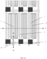
- FIGS. 2A-2F illustrate an array substrate not according to the claimed invention.
- the array substrate 1 comprises a plurality of touch control signal lines 3, a plurality of gate lines 4 and a plurality of data lines 5.
- the plurality of data lines 5 and the plurality of gate lines 4 are arranged to cross with each other to thereby define a plurality of pixel subunits.
- each pixel subunit is substantially a region defined by two adjacent data lines and two adjacent gate lines that stagger to one another, i.e., an orthographic projection of each region formed by two adjacent data lines and two adjacent gate lines substantially defines a pixel subunit.
- one pixel subunit is indicated by the bigger box with dotted lines 100, with one side of the pixel subunit substantially between the middle line of the two adjacent data lines 5.
- another side of the pixel subunit that is perpendicular to the aforementioned side of the pixel subunit is between the middle line of the two adjacent gate lines 4 (not shown in the drawings). It is noted that such definition for pixel subunit shall be applied throughout the disclosure.
- Each of the plurality of touch control signal lines 3 is arranged within opening regions of the pixel subunits. Specifically, each touch control signal line 3 is arranged within the opening region of any one of the pixel subunits of each pixel unit (i.e. an orthographic projection of each touch control signal line 3 on a plane, such as the substrate of the array substrate, is within an orthographic projection of the opening region of one of the pixel subunits of the pixel unit on the same plane), and is further arranged to be substantially in parallel with one of the plurality of data lines 5.
- a predetermined number of pixel subunits are configured to form a pixel unit.
- FIG. 2A which serves as an illustrating example, three pixel subunits, R (red), G (green) and B (blue), form a pixel unit.
- Each touch control signal line 3 is arranged at an opening region of one R pixel subunit of each pixel unit.
- an encasing substrate 2 can be disposed to oppose to the array substrate 1 in a touch control display panel.
- a pattern of a black matrix 6 is disposed over a surface of the encasing substrate 2 that is proximal to the array substrate 1 (as shown to be below the encasing substrate 2 in the figures).
- the black matrix 6 is configured to cover each of the plurality of gate lines 4 and each of the plurality of data lines 5 (i.e. an orthographic projection of each of the plurality of gate lines 4 and each of the plurality of data lines 5 on a plane, such as the substrate of the array substrate, is within an orthographic projection of the black matrix 6 on the same plane).
- the pattern of the black matrix 6 is in a shape of a mesh, and contains a plurality of openings defined by the intercrossing wires of the mesh structure of the black matrix 6.
- Each of the plurality of openings of the mesh-shaped black matrix 6 corresponds to one opening region of the pixel subunits (i.e. an orthographic projection of each opening of the black matrix 6 on the substrate overlaps with an orthographic projection of each opening region of pixel subunits on the substrate).
- each touch control signal line 3 is arranged at one opening region of the pixel subunits, the orthographic projection of the black matrix 6 on the substrate does not cover the orthographic projection of each touch control signal line 3 on the substrate.
- FIG. 1B shows the positional arrangement of the black matrix 6, each touch control signal line 3, each data line 5, and their relative distance relationship in an array substrate of a conventional touch control display panel.
- the width of a pixel unit is p (that is, the sum of the widths of the three pixel subunits, R, G, and B, is p), the width of each first wire of the black matrix 6 that covers each touch control signal line 3 is mx, the width of each second wire of the black matrix 6 that does not cover any touch control signal line 3 is m, the width of each touch control signal line 3 is w, the distance between each touch control signal line 3 and a neighboring data line 5 is s, the distance between an end of each touch control signal line 3 that is distal to, or far away from, the neighboring data line 5 and a corresponding end of the corresponding wire of the black matrix 6 is a, the distance between an end of the neighboring data line 5 that is proximal to, or close to, the neighboring touch control signal line 3 and the other end of the wire of the black matrix 6 is b.
- FIG. 2B shows the positional arrangement of the black matrix 6, each touch control signal line 3, each data line 5, and their relative distance relationship in an array substrate according to some embodiments of the disclosure.
- the width of the pixel unit is p
- the width of each touch control signal line 3 is w. Because each touch control signal line 3 is arranged at the opening region of the pixel subunits, the wires of the black matrix 6 do not cover the each touch control signal line 3.
- the widths of all wires in the back matrix 6 are the same, and they are all m.
- each touch control signal line 3 is not covered by the pattern of the black matrix 6 (more specifically, the wires of the black matrix 6), or in other words, an orthographic projection of each touch control signal line 3 on a plane, such as the substrate of the array substrate, is not overlapped with an orthographic projection of the black matrix 6 in the opening regions on the same plane.
- the width of each wire of the black matrix 6 can be reduced, thereby the aperture ratio of the pixel units, and the light transmittance of the touch control display panel containing the array substrate, and the display apparatus comprising the touch control display panel as well, can be improved. Accordingly, the display effect of the display apparatus can be improved.
- each touch control signal line 3 is arranged in a middle of an opening region of each pixel subunit. In other words, the distances between a touch control signal line 3 and the two data lines 2 that are immediately adjacent to the touch control signal line 3 are substantially equal.
- each touch control signal line 3 in the middle of the opening region of the pixel subunits, a distance between each touch control signal line 3 and a data line 5 can be maximally increased. As a result, the risk of a short circuiting between a touch control signal line 3 and a data line 5 can be reduced, and the yield rate of the touch control display panel products can be improved.
- each touch control signal line 3 and the two data lines 5 that are immediately adjacent to the touch control signal line 3 are substantially equal, the influences of the two data line 5 on the voltages over the pixel electrodes inside two neighboring pixel subunits are substantially the same. As a result, the deviation of the display effect between the two neighboring pixel subunits can be avoided, and the display effect can be further improved.
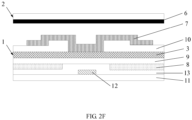
- the array substrate 1 comprises a substrate 11, a plurality of gate electrodes 12, a gate insulating layer 13, a plurality of data lines 5, a plurality of first electrodes 7, a plurality of second electrodes 8, a first passivation layer 9, a plurality of touch control signal lines 3, and a second passivation layer 10.
- the plurality of gate electrodes 12, the gate insulating layer 13, the plurality of data lines 5 and the plurality of second electrodes 8, the first passivation layer 9, the plurality of touch control signal lines 3, the second passivation layer 10, and the plurality of first electrodes 7 are disposed sequentially over the substrate 11.
- the plurality of gate electrodes 12 are each electrically coupled to one gate line 4.
- Each of the plurality of second electrodes 8 is block-shaped, and each of the plurality of first electrode 7 is strip-shaped.
- Each second electrode 8 is arranged at an opening region of each pixel subunit (i.e. an orthographic projection of each second electrode 8 on the substrate is contained within an orthographic projection of the opening region of each pixel subunit on the substrate), and is configured as a pixel electrode.
- Each first electrode 7 is strip-shaped, and is configured as a common electrode.
- each of the plurality of touch control signal lines 3 is arranged between the plurality of first electrodes 7 and the plurality of second electrodes 8 along a direction perpendicular to the array substrate 1 (more specifically, the substrate 11 of the array substrate 1).
- each touch control signal line 3 is electrically connected to one of the plurality of first electrodes 7 corresponding to the each touch control signal line 3 through a via 14 that is arranged in, and penetrates, the second passivation layer 10.
- each touch control signal line 3 is configured to provide common voltage signals to the one of the plurality of first electrodes 7 corresponding thereto, and the one of the plurality of first electrodes 7 accordingly serves as a common electrode.
- the one of the plurality of first electrodes 7 is configured as a touch control electrode, and each touch control signal line 3 is configured to provide touch control driving signals to the one of the plurality of first electrodes 7 (i.e. touch control electrode) and is also configured to receive response signals.
- the finger and one or more of the plurality of first electrodes 7 in the array substrate 1 within a touch control region of the touch control display panel can form one or more capacitors, and a voltage over each of the one or more first electrodes 7 within the touch control region is altered or changed as such.
- the positions of the touch control region can be determined through testing the change of the voltage over each of the one or more first electrodes 7 within the touch control region.
- an electric field is formed between each of the plurality of first electrodes 7 and a corresponding second electrode 8 (i.e. a second electrode 8 whose orthographic projection on the substrate covers an orthographic projection of the each of the plurality of first electrodes 7 on the substrate) to drive a liquid crystal layer (not shown in the drawings) that is arranged between the array substrate 1 and the encasing substrate 2 to twist, thereby realizing an image display of the touch control display panel.
- a liquid crystal layer not shown in the drawings
- an orthographic projection of each touch control signal line 3 on the substrate 11 of the array substrate 1 can be configured to be overlapped both with an orthographic projection of a corresponding first electrode 7 on the substrate 11 of the array substrate 1, and with an orthographic projection of a corresponding second electrode 8 on the substrate 11 of the array substrate 1.
- each of the plurality of touch control signal lines 3 can be configured to have a special positional relationship with each second electrode 8 and/or each first electrode 7 corresponding thereto.
- each touch control signal line 3 has a different configurations of each touch control signal line 3, and its positional relationship with a corresponding first electrode 7 and a corresponding second electrode 8, according to three different embodiments of the array substrate will be described in detail.
- the plurality of touch control signal lines 3, the plurality of first electrode 7, and the plurality of second electrodes 8 are configured such that each touch control signal line 3 is not arranged at a location where a second electrode 8 corresponding to the each touch control signal line 3 is located (i.e. each second electrode 8 is disconnected at a region corresponding to a touch control signal line 3), but each touch control signal line 3 is still arranged at a location where a first electrode 7 corresponding to the each touch control signal line 3 is located.
- the plurality of touch control signal lines 3, the plurality of first electrode 7, and the plurality of second electrodes 8 are configured such that each touch control signal line 3 is not arranged at a location where a first electrode 7 corresponding to the each touch control signal line 3 is located, but each touch control signal line 3 is still arranged at a location where a second electrode 8 corresponding to the each touch control signal line 3 is located.
- the plurality of touch control signal lines 3, the plurality of first electrode 7, and the plurality of second electrodes 8 are configured such that each touch control signal line 3 is not arranged at a location where a first electrode 7 corresponding to the each touch control signal line 3 is located, and is further not arranged at a location where a second electrode 8 corresponding to the each touch control signal line 3 is located (i.e. each second electrode 8 is disconnected at a region corresponding to a touch control signal line 3).
- each touch control signal line 3 is arranged neither at a location where a corresponding first electrode 7 is located nor at a location where a corresponding second electrode 8 is located, each of the plurality of touch control signal lines 3 in the third embodiment has the lowest electric resistance.
- each touch control signal line 3 is still arranged at a location where a corresponding first electrode 7 is located (as in the first embodiment shown in FIG. 2D ) or where a corresponding second electrode 8 is located (in the second embodiment shown in FIG. 2C ) is located, the effect of reducing the electric resistance of each of the plurality of touch control signal lines 3 in any of these two embodiments is not as good as the third embodiment.
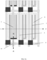
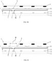
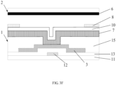
- FIGS. 3A-3F illustrate an array substrate according to some other embodiments of the disclosure.
- the array substrate according to the embodiments as illustrated in FIGS. 3A-3F comprises an organic resin layer (ORG), and the plurality of touch control signal lines 3 and the plurality of data lines 5 are configured at a substantially same layer and have a substantially same composition. Due to this latter feature as mentioned above, in the embodiments of the array substrate as illustrated in FIGS. 3A-3F , the plurality of touch control signal lines 3 and the plurality of data lines 5 can be formed through a one-time patteming process during a manufacturing process of the array substrate 1.
- ORG organic resin layer
- the plurality of touch control signal lines 3 are not arranged between the plurality of first electrodes 7 and the plurality of second electrodes 8 as in the embodiments of the array substrate illustrated in FIGS. 2A-2F , but are arranged over a side of the organic resin layer that is distal to (i.e. far away from) the plurality of first electrodes 7.
- the plurality of touch control signal lines 3 and the plurality of data lines 5 are configured at a substantially same layer and have a substantially same composition, and an organic resin layer 15 is further arranged in the array substrate 1. More specifically, the organic resin layer 15 is arranged at a side of a layer of the plurality of touch control signal lines 3 and the plurality of data lines 5 that is proximal to the encasing substrate 2 (i.e. distal to the substrate 11 of the array substrate 1).
- the array substrate comprises a plurality of gate electrodes 12, a gate insulating layer 13, the above-mentioned layer of the plurality of touch control signal lines 3 and the plurality of data lines 5, the above-mentioned organic resin layer 15, a plurality of first electrodes 7, a second passivation layer 10, and a plurality of second electrodes 8, which are sequentially or successively disposed over a substrate 11 of the array substrate 1.
- each of the plurality of gate electrode 12 are electrically coupled to one of the plurality of gate lines 4.
- Each of the plurality of second electrodes 8 is strip-shaped and is arranged at an opening region of each of the pixel subunits (i.e. an orthographic projection of each second electrode 8 on the substrate 11 is contained within an orthographic projection of the opening region of each of the pixel subunits on the substrate 11).
- Each second electrode 8 can be configured as a pixel electrode in these embodiments of the array substrate as described herein.
- Each of the plurality of first electrode 7 is block-shaped, and can be configured to serve as a common electrode in these embodiments of the array substrate as described herein.
- the plurality of first electrode 7 and the plurality of second electrodes 8 are arranged at a side of the organic resin layer 15 that is distal to the above mentioned layer of the plurality of touch control signal lines 3 and the plurality of data lines 5.
- the organic resin layer 15 is sandwiched between the layer of the plurality of touch control signal lines 3 and the plurality of data lines 5 and the plurality of first electrode 7 and the plurality of second electrodes 8.
- each of the plurality of touch control signal lines 3 is electrically connected to one of the plurality of first electrodes 7 that corresponds thereto through a via that is arranged in, and penetrates, the organic resin layer 15.
- each touch control signal line 3 is configured to provide common voltage signals to the one of the plurality of first electrodes 7 corresponding thereto, and the one of the plurality of first electrodes 7 accordingly serves as a common electrode.
- the one of the plurality of first electrodes 7 is configured as a touch control electrode, and each touch control signal line 3 is configured to provide touch control driving signals to the one of the plurality of first electrodes 7 (i.e. touch control electrode) and is also configured to receive response signals.
- the organic resin layer 15 in the embodiments of the array substrate as illustrated in FIGS. 3A-3F and described herein replaces the one passivation layer (i.e. the first passivation layer 9) in the embodiments of the array substrate as illustrated in FIGS. 2A-2F .
- Such a replacement causes the embodiments of the array substrate as illustrated in FIGS. 3A-3F to have the following technical advantages over the embodiments of the array substrate as illustrated in FIGS. 2A-2F .
- the composition in the organic resin layer 15 typically has a relatively lower dielectric constant
- the capacitor formed substantially between the plurality of touch control signal lines 3 and the plurality of first electrodes 7 and/or between the plurality of touch control signal lines 3 and the plurality of second electrodes 8 in the embodiments of the array substrate as illustrated in FIGS. 3A-3F and described herein where the organic resin layer is employed can have a reduced capacitance compared with the embodiments of the array substrate as illustrated in FIGS. 2A-2F and described above where the second passivation layer 10 is employed.
- the organic resin layer 15 can be configured to have a relatively larger thickness.
- the distance between the plurality of touch control signal lines 3 and the plurality of first electrodes 7 and/or the distance between the plurality of touch control signal lines 3 and the plurality of second electrodes 8 can be relatively larger in the embodiments of the array substrate as illustrated in FIGS. 3A-3F and described herein compared with the embodiments of the array substrate as illustrated in FIGS. 2A-2F and described above.
- This feature in turn can further lead to a reduction, to some degree, of the electric resistance of each of the plurality of touch control signal lines 3 in the embodiments of the array substrate as illustrated in FIGS. 3A-3F and described herein.
- each touch control signal lines 3 in terms of its positional relationship with each first electrode 7 and/or each second electrode 8 corresponding thereto (e.g. by arranging each touch control signal lines 3 not to be at a location where a corresponding first electrode 7 and/or a corresponding second electrode 8 is located), as in the embodiments of the array substrate as illustrated in FIGS. 2A-2F and described above, because the electric resistance of each of the plurality of touch control signal lines 3 can be reduced by replacement of the one passivation layer by the organic resin layer 15. As such, the driving frequency of each of the plurality of touch control signal lines 3 in these embodiments described herein can be improved.
- each of the plurality of touch control signal lines 3 is configured to have a special positional relationship with each second electrode 8 and/or each first electrode 7 corresponding thereto, similar to the embodiments of the array substrate as illustrated in FIGS. 2A-2F and described above.
- each touch control signal line 3 has a different configurations of each touch control signal line 3, and its positional relationship with a corresponding first electrode 7 and a corresponding second electrode 8, according to three different embodiments of the array substrate will be described in detail.
- the plurality of touch control signal lines 3, the plurality of first electrode 7, and the plurality of second electrodes 8 are configured such that each touch control signal line 3 is not arranged at a location where a first electrode 7 corresponding to the each touch control signal line 3 is located (i.e. each first electrode 7 is disconnected at a region corresponding to a touch control signal line 3), but each touch control signal line 3 is still arranged at a location where a second electrode 8 corresponding thereto the each touch control signal line 3 is located.
- the plurality of touch control signal lines 3, the plurality of first electrode 7, and the plurality of second electrodes 8 are configured such that each touch control signal line 3 is not arranged at a location where a second electrode 8 corresponding to the each touch control signal line 3 is located, but each touch control signal line 3 is still arranged at a location where a first electrode 7 corresponding to the each touch control signal line 3 is located.
- the plurality of touch control signal lines 3, the plurality of first electrode 7, and the plurality of second electrodes 8 are configured such that each touch control signal line 3 is not arranged at a location where a first electrode 7 corresponding to the each touch control signal line 3 is located, and is further not arranged at a location where a second electrode 8 corresponding to the each touch control signal line 3 is located.
- each touch control signal line 3 is arranged neither at a location where a corresponding first electrode 7 is located nor at a location where a corresponding second electrode 8 is located, each of the plurality of touch control signal lines 3 in the third embodiment has the lowest electric resistance.
- each touch control signal line 3 is still arranged at a location where a corresponding first electrode 7 is located (as in the fifth embodiment shown in FIG. 3D ) or where a corresponding second electrode 8 is located (in the fourth embodiment shown in FIG. 3B ) is located, the effect of reducing the electric resistance of each of the plurality of touch control signal lines 3 in any of these two embodiments is not as good as the sixth embodiment.
- the present disclosure further provides a touch control display panel.
- the touch control display panel comprises an array substrate 1 and an encasing substrate 2, opposing to each other.
- a black matrix 6 is arranged over a side of the encasing substrate 2 facing the array substrate 1, configured such that each of the plurality of touch control signal lines 3 is arranged at an opening region of the black matrix 6.
- an orthographic projection of each of the plurality of touch control signal lines 3 on the substrate 1 (or the encasing substrate 2) is contained within an orthographic projection of each opening region of the black matrix 6 on the substrate 1 (or the encasing substrate 2).
- each of the plurality of touch control signal lines 3 is thus not covered by the black matrix 6.
- the corresponding width of the black matrix 6 can be reduced, in turn resulting in an improved pixel aperture ratio and light improved light transmittance rate of the touch control display panel, ultimately leading to an improved display effect.
- the present disclosure further provides a display apparatus.
- the display apparatus comprises the touch control display panel according to any of the embodiments as described above.
- the display apparatus herein is substantially a touch control display apparatus.
- the touch control signal line 3 will not be covered by the black matrix 6, therefore, the corresponding width of the black matrix 6 can be reduced, therefore the pixel aperture ratio is improved and the light transmittance of the touch control display panel is improved, the display effect is improved accordingly.
Landscapes
- Physics & Mathematics (AREA)
- Engineering & Computer Science (AREA)
- Nonlinear Science (AREA)
- General Physics & Mathematics (AREA)
- General Engineering & Computer Science (AREA)
- Theoretical Computer Science (AREA)
- Crystallography & Structural Chemistry (AREA)
- Mathematical Physics (AREA)
- Chemical & Material Sciences (AREA)
- Optics & Photonics (AREA)
- Human Computer Interaction (AREA)
- Microelectronics & Electronic Packaging (AREA)
- Devices For Indicating Variable Information By Combining Individual Elements (AREA)
- Liquid Crystal (AREA)
- Position Input By Displaying (AREA)
Claims (14)
- Berührungsgesteuerte Anzeigetafel, umfassend ein Array-Substrat (1), wobei das Array-Substrat (1) Folgendes umfasst:ein Substrat (11);eine Pixeleinheit über dem Substrat (11), die eine Vielzahl von Pixel-Untereinheiten umfasst; undeine Berührungssteuerungssignalleitung (3) über dem Substrat (11); undeine Vielzahl von Datenleitungen (5) und eine Vielzahl von Gate-Leitungen (4) über dem Substrat, die zueinander versetzt sind, so dass eine orthographische Projektion jedes Bereichs, der durch zwei benachbarte Datenleitungen und zwei benachbarte Gate-Leitungen gebildet wird, eine Pixel-Untereinheit definiert,wobei:eine orthographische Projektion der Berührungssteuerungssignalleitung (3) auf dem Substrat (11) in einem Öffnungsbereich einer der Vielzahl von Pixel-Untereinheiten auf dem Substrat (11) angeordnet ist,wobei die eine der Vielzahl von Pixel-Untereinheiten eine erste Elektrode (7) und eine zweite Elektrode (8) über dem Substrat (11) umfasst, wobei mindestens eine der ersten Elektrode (7) und der zweiten Elektrode (8) mindestens eine Lücke umfasst, die jeweils zwischen zwei benachbarten Abschnitten von jeder der mindestens einen der ersten Elektrode (7) und der zweiten Elektrode (8) angeordnet ist; und eine orthographische Projektion der Berührungssteuerungssignalleitung (3) auf dem Substrat (11) innerhalb einer orthographischen Projektion einer der mindestens einen Lücke in einer oder beiden der mindestens einen der ersten Elektrode (7) und der zweiten Elektrode (8) auf dem Substrat (11) enthalten ist, undwobei sich die Berührungssteuerungssignalleitung (3) und die Vielzahl von Datenleitungen (5) in einer gleichen Schicht befinden und im Wesentlichen die gleiche Zusammensetzung aufweisen, und die Berührungssteuerungssignalleitung (3) und die Vielzahl von Datenleitungen (5) in die gleiche Richtung verlaufen.
- Berührungsgesteuerte Anzeigetafel nach Anspruch 1, wobei:die erste Elektrode (7) mindestens einen ersten Zwischenraum (G2) aufweist, der jeweils zwischen zwei benachbarten ersten Abschnitten der ersten Elektrode (7) angeordnet ist; unddie orthographische Projektion der Berührungssteuerungssignalleitung (3) auf dem Substrat (11) innerhalb einer orthographischen Projektion eines der mindestens einen ersten Zwischenräume (G2) in der ersten Elektrode (7) auf dem Substrat (11) liegt und mit einer orthographischen Projektion der zweiten Elektrode (8) überlappt.
- Berührungsgesteuerte Anzeigetafel nach Anspruch 1, wobei:die zweite Elektrode (8) mindestens einen zweiten Zwischenraum (G1) aufweist, der jeweils zwischen zwei benachbarten zweiten Abschnitten der zweiten Elektrode (8) angeordnet ist; unddie orthographische Projektion der Berührungssteuerungssignalleitung (3) auf dem Substrat (11) innerhalb einer orthographischen Projektion eines der mindestens einen zweiten Zwischenräume (G1) in der zweiten Elektrode (8) auf dem Substrat (11) liegt undmit einer orthographischen Projektion der ersten Elektrode (7) überlappt.
- Berührungsgesteuerte Anzeigetafel nach Anspruch 1, wobei:die erste Elektrode (7) mindestens einen ersten Zwischenraum (G2) aufweist, der jeweils zwischen zwei benachbarten ersten Abschnitten der ersten Elektrode (7) angeordnet ist;die zweite Elektrode (8) mindestens einen zweiten Zwischenraum (G1) aufweist, der jeweils zwischen zwei benachbarten zweiten Abschnitten der zweiten Elektrode (8) angeordnet ist; unddie orthographische Projektion der Berührungssteuerungssignalleitung (3) auf dem Substrat (11) sowohl innerhalb einer orthographischen Projektion eines der mindestens einen ersten Zwischenräume (G2) in der ersten Elektrode (7) auf dem Substrat (11) als auch innerhalb einer orthographischen Projektion eines der mindestens einen zweiten Zwischenräume (G1) in der zweiten Elektrode (8) auf dem Substrat (11) enthalten ist.
- Berührungsgesteuerte Anzeigetafel nach Anspruch 1, wobei:die erste Elektrode (7) so konfiguriert ist, dass sie als gemeinsame Elektrode dient;die zweite Elektrode (8) so konfiguriert ist, dass sie als Pixelelektrode dient; unddie Berührungssteuerungssignalleitung (3) elektrisch mit der ersten Elektrode (7) gekoppelt ist.
- Berührungsgesteuerte Anzeigetafel nach Anspruch 5, wobei die erste Elektrode (7) während einer Berührungssteuerungsphase als Berührungssteuerungselektrode und während einer Anzeigephase als gemeinsame Elektrode konfiguriert ist.
- Berührungsgesteuerte Anzeigetafel nach Anspruch 4, wobei die eine der Vielzahl von Pixel-Untereinheiten ferner eine Isolierschicht umfasst, die zwischen der Berührungssteuerungssignalleitung (3) und der ersten Elektrode (7) angeordnet ist, wobei die Berührungssteuerungssignalleitung (3) durch eine Durchkontaktierung in der Isolierschicht elektrisch mit der ersten Elektrode (7) gekoppelt ist.
- Berührungsgesteuerte Anzeigetafel nach Anspruch 1, wobei die Berührungssteuerungssignalleitung (3) über einer Seite der ersten Elektrode (7) verläuft, die distal zur zweiten Elektrode (8) entlang einer Richtung senkrecht zum Substrat (11) liegt.
- Berührungsgesteuerte Anzeigetafel nach Anspruch 8, wobei die berührungsgesteuerte Anzeigetafel ferner eine Passivierungsschicht zwischen der ersten Elektrode (7) und der zweiten Elektrode (8) entlang der Richtung senkrecht zum Substrat (11) umfasst.
- Berührungsgesteuerte Anzeigetafel nach Anspruch 1, wobei die Berührungssteuerungssignalleitung (3) zwischen der ersten Elektrode (7) und der zweiten Elektrode (8) liegt.
- Berührungsgesteuerte Anzeigetafel nach Anspruch 10, das ferner eine erste Passivierungsschicht (9) und eine zweite Passivierungsschicht (10) umfasst, wobei entlang der Richtung senkrecht zum Substrat (11):die erste Passivierungsschicht (9) zwischen der Berührungssteuerungssignalleitung (3) und der zweiten Elektrode (8) liegt; unddie zweite Passivierungsschicht (10) zwischen der Berührungssteuerungssignalleitung (3) und der ersten Elektrode (7) liegt.
- Berührungsgesteuerte Anzeigetafel nach einem der Ansprüche 1 bis 11, wobei die Berührungssteuerungssignalleitung (3) im Wesentlichen den gleichen Abstand zu jeder der zwei benachbarten Datenleitungen (5) aufweist, die die eine der Vielzahl von Pixel-Untereinheiten definieren.
- Berührungsgesteuerte Anzeigetafel nach einem der Ansprüche 1 bis 12, das ferner ein umhüllendes Substrat (2) über einer dem Substrat (11) abgewandten Seite des Array-Substrats (1) umfasst.
- Berührungsgesteuerte Anzeigetafel nach Anspruch 13, das ferner eine schwarze Matrix (6) über einer Seite des umschließenden Substrats (2) in der Nähe des Substrats (11) umfasst, wobei:die schwarze Matrix (6) eine Vielzahl von Öffnungen aufweist; unddie schwarze Matrix (6) so konfiguriert ist, dass eine orthographische Projektion jeder der Vielzahl von Pixel-Untereinheiten innerhalb einer orthographischen Projektion jeder Öffnung der schwarzen Matrix (6) auf dem Substrat (11) enthalten ist.
Applications Claiming Priority (2)
| Application Number | Priority Date | Filing Date | Title |
|---|---|---|---|
| CN201710675303.7A CN109388265B (zh) | 2017-08-09 | 2017-08-09 | 一种阵列基板、触控显示面板及显示装置 |
| PCT/CN2018/079989 WO2019029167A1 (en) | 2017-08-09 | 2018-03-22 | TOUCH CONTROL DISPLAY PANEL |
Publications (3)
| Publication Number | Publication Date |
|---|---|
| EP3665556A1 EP3665556A1 (de) | 2020-06-17 |
| EP3665556A4 EP3665556A4 (de) | 2021-04-28 |
| EP3665556B1 true EP3665556B1 (de) | 2025-05-07 |
Family
ID=65270842
Family Applications (1)
| Application Number | Title | Priority Date | Filing Date |
|---|---|---|---|
| EP18769581.2A Active EP3665556B1 (de) | 2017-08-09 | 2018-03-22 | Berührungsgesteuerte anzeigetafel |
Country Status (5)
| Country | Link |
|---|---|
| US (1) | US11157103B2 (de) |
| EP (1) | EP3665556B1 (de) |
| JP (1) | JP7052966B2 (de) |
| CN (1) | CN109388265B (de) |
| WO (1) | WO2019029167A1 (de) |
Families Citing this family (16)
| Publication number | Priority date | Publication date | Assignee | Title |
|---|---|---|---|---|
| CN109557728B (zh) * | 2017-09-25 | 2021-12-10 | 京东方科技集团股份有限公司 | 像素结构及其制作方法、阵列基板和触控显示装置 |
| CN110085126A (zh) * | 2019-05-10 | 2019-08-02 | 深圳市华星光电半导体显示技术有限公司 | 组合式显示面板 |
| CN111708237B (zh) * | 2020-06-30 | 2023-06-06 | 上海中航光电子有限公司 | 一种阵列基板、显示面板及显示装置 |
| CN112130697B (zh) * | 2020-09-29 | 2024-06-14 | 武汉天马微电子有限公司 | 一种触控显示面板和显示装置 |
| CN114967986B (zh) * | 2021-02-25 | 2025-06-27 | 合肥京东方光电科技有限公司 | 触控显示面板及显示装置 |
| CN112905052B (zh) * | 2021-03-05 | 2024-08-13 | 合肥京东方光电科技有限公司 | 阵列基板及其制备方法、触控显示装置 |
| CN112860117B (zh) * | 2021-03-05 | 2024-01-26 | 京东方科技集团股份有限公司 | 阵列基板及其制备方法、触控显示装置 |
| EP4202613B1 (de) * | 2021-05-28 | 2025-12-31 | BOE Technology Group Co., Ltd. | Arraysubstrat und herstellungsverfahren dafür sowie anzeigevorrichtung |
| US12140842B2 (en) | 2021-06-18 | 2024-11-12 | Beijing Boe Display Technology Co., Ltd. | Display substrate and preparation method therefor, display device, and mask |
| CN115268132B (zh) | 2022-07-19 | 2023-08-22 | 武汉华星光电技术有限公司 | 显示装置及其显示面板 |
| US12379800B2 (en) * | 2023-02-21 | 2025-08-05 | Beijing Boe Display Technology Co., Ltd. | Display substrate, display panel and display apparatus |
| JP2024141516A (ja) * | 2023-03-29 | 2024-10-10 | シャープディスプレイテクノロジー株式会社 | アクティブマトリクス基板、タッチセンサ機能付き表示パネル、及びアクティブマトリクス基板の製造方法 |
| CN116819817B (zh) * | 2023-06-27 | 2026-02-06 | 厦门天马微电子有限公司 | 显示面板和显示装置 |
| CN120188097A (zh) * | 2023-09-28 | 2025-06-20 | 京东方科技集团股份有限公司 | 显示基板 |
| CN118444506A (zh) | 2024-05-08 | 2024-08-06 | 厦门天马光电子有限公司 | 一种显示面板和显示装置 |
| CN119511591A (zh) * | 2024-12-13 | 2025-02-25 | 厦门天马微电子有限公司 | 显示面板及显示装置 |
Citations (1)
| Publication number | Priority date | Publication date | Assignee | Title |
|---|---|---|---|---|
| US20170115784A1 (en) * | 2015-10-23 | 2017-04-27 | Boe Technology Group Co., Ltd. | Self-capacitance touch display panel and method of driving the same, and touch display device |
Family Cites Families (8)
| Publication number | Priority date | Publication date | Assignee | Title |
|---|---|---|---|---|
| TWM459453U (zh) * | 2013-01-10 | 2013-08-11 | Inv Element Inc | 於下基板設置金屬感應層之內嵌式觸控顯示面板結構 |
| CN103353683B (zh) * | 2013-06-26 | 2016-02-10 | 京东方科技集团股份有限公司 | 一种阵列基板以及包括该阵列基板的显示装置 |
| WO2015059995A1 (ja) * | 2013-10-22 | 2015-04-30 | シャープ株式会社 | タッチセンサ付き表示装置 |
| CN104536637A (zh) * | 2015-01-29 | 2015-04-22 | 京东方科技集团股份有限公司 | 内嵌式触摸屏及显示装置 |
| CN108646453A (zh) * | 2015-05-08 | 2018-10-12 | 厦门天马微电子有限公司 | 触控阵列基板、液晶显示面板和液晶显示装置 |
| CN105093736A (zh) | 2015-07-14 | 2015-11-25 | 京东方科技集团股份有限公司 | Ips阵列基板及其制作方法、显示器件 |
| JP6514593B2 (ja) * | 2015-07-17 | 2019-05-15 | パナソニック液晶ディスプレイ株式会社 | タッチ検出機能付表示装置 |
| KR102554251B1 (ko) * | 2015-12-07 | 2023-07-11 | 엘지디스플레이 주식회사 | 표시장치 |
-
2017
- 2017-08-09 CN CN201710675303.7A patent/CN109388265B/zh active Active
-
2018
- 2018-03-22 EP EP18769581.2A patent/EP3665556B1/de active Active
- 2018-03-22 WO PCT/CN2018/079989 patent/WO2019029167A1/en not_active Ceased
- 2018-03-22 US US16/088,519 patent/US11157103B2/en active Active
- 2018-03-22 JP JP2019503527A patent/JP7052966B2/ja active Active
Patent Citations (1)
| Publication number | Priority date | Publication date | Assignee | Title |
|---|---|---|---|---|
| US20170115784A1 (en) * | 2015-10-23 | 2017-04-27 | Boe Technology Group Co., Ltd. | Self-capacitance touch display panel and method of driving the same, and touch display device |
Also Published As
| Publication number | Publication date |
|---|---|
| JP7052966B2 (ja) | 2022-04-12 |
| EP3665556A4 (de) | 2021-04-28 |
| EP3665556A1 (de) | 2020-06-17 |
| JP2020529640A (ja) | 2020-10-08 |
| CN109388265A (zh) | 2019-02-26 |
| US11157103B2 (en) | 2021-10-26 |
| US20210011570A1 (en) | 2021-01-14 |
| WO2019029167A1 (en) | 2019-02-14 |
| CN109388265B (zh) | 2023-02-28 |
Similar Documents
| Publication | Publication Date | Title |
|---|---|---|
| US11157103B2 (en) | Touch control display panel | |
| US10838533B2 (en) | Display device and liquid crystal display device with built-in touch panel | |
| US10013090B2 (en) | Self-capacitance touch display panel and method of driving the same, and touch display device | |
| US8669920B2 (en) | Pixel array | |
| EP2701040A2 (de) | Kapazitiver Berührungsbildschirm in der Zelle und Anzeigevorrichtung | |
| CN107121804B (zh) | 显示装置 | |
| CN105022184A (zh) | 显示装置 | |
| CN107678590B (zh) | 一种触控显示面板及其驱动方法 | |
| TW201616304A (zh) | 內嵌式觸控顯示面板 | |
| US10514789B2 (en) | Integrated touch control display panel and display device | |
| US20210165532A1 (en) | Detection substrate and display device | |
| US10884542B2 (en) | Display device | |
| US9835919B2 (en) | Display device including a plurality of metal lines in contact with a common electrode | |
| JP6240278B2 (ja) | タッチパネル内蔵型液晶表示装置 | |
| JP3279929B2 (ja) | 液晶表示装置 | |
| JP6410908B2 (ja) | タッチパネル内蔵型液晶表示装置 | |
| US20150084845A1 (en) | Liquid Crystal Display Device |
Legal Events
| Date | Code | Title | Description |
|---|---|---|---|
| STAA | Information on the status of an ep patent application or granted ep patent |
Free format text: STATUS: UNKNOWN |
|
| STAA | Information on the status of an ep patent application or granted ep patent |
Free format text: STATUS: THE INTERNATIONAL PUBLICATION HAS BEEN MADE |
|
| PUAI | Public reference made under article 153(3) epc to a published international application that has entered the european phase |
Free format text: ORIGINAL CODE: 0009012 |
|
| STAA | Information on the status of an ep patent application or granted ep patent |
Free format text: STATUS: REQUEST FOR EXAMINATION WAS MADE |
|
| 17P | Request for examination filed |
Effective date: 20180927 |
|
| AK | Designated contracting states |
Kind code of ref document: A1 Designated state(s): AL AT BE BG CH CY CZ DE DK EE ES FI FR GB GR HR HU IE IS IT LI LT LU LV MC MK MT NL NO PL PT RO RS SE SI SK SM TR |
|
| AX | Request for extension of the european patent |
Extension state: BA ME |
|
| DAV | Request for validation of the european patent (deleted) | ||
| DAX | Request for extension of the european patent (deleted) | ||
| R17P | Request for examination filed (corrected) |
Effective date: 20180927 |
|
| REG | Reference to a national code |
Ref country code: DE Ref legal event code: R079 Free format text: PREVIOUS MAIN CLASS: G06F0003041000 Ipc: G02F0001133300 Ref country code: DE Ref legal event code: R079 Ref document number: 602018081741 Country of ref document: DE Free format text: PREVIOUS MAIN CLASS: G06F0003041000 Ipc: G02F0001133300 |
|
| A4 | Supplementary search report drawn up and despatched |
Effective date: 20210326 |
|
| RIC1 | Information provided on ipc code assigned before grant |
Ipc: G02F 1/1333 20060101AFI20210322BHEP Ipc: G02F 1/1362 20060101ALI20210322BHEP Ipc: G06F 3/041 20060101ALI20210322BHEP |
|
| GRAP | Despatch of communication of intention to grant a patent |
Free format text: ORIGINAL CODE: EPIDOSNIGR1 |
|
| STAA | Information on the status of an ep patent application or granted ep patent |
Free format text: STATUS: GRANT OF PATENT IS INTENDED |
|
| INTG | Intention to grant announced |
Effective date: 20241119 |
|
| GRAS | Grant fee paid |
Free format text: ORIGINAL CODE: EPIDOSNIGR3 |
|
| GRAA | (expected) grant |
Free format text: ORIGINAL CODE: 0009210 |
|
| STAA | Information on the status of an ep patent application or granted ep patent |
Free format text: STATUS: THE PATENT HAS BEEN GRANTED |
|
| AK | Designated contracting states |
Kind code of ref document: B1 Designated state(s): AL AT BE BG CH CY CZ DE DK EE ES FI FR GB GR HR HU IE IS IT LI LT LU LV MC MK MT NL NO PL PT RO RS SE SI SK SM TR |
|
| REG | Reference to a national code |
Ref country code: GB Ref legal event code: FG4D |
|
| REG | Reference to a national code |
Ref country code: CH Ref legal event code: EP |
|
| REG | Reference to a national code |
Ref country code: DE Ref legal event code: R096 Ref document number: 602018081741 Country of ref document: DE |
|
| REG | Reference to a national code |
Ref country code: IE Ref legal event code: FG4D |
|
| REG | Reference to a national code |
Ref country code: NL Ref legal event code: MP Effective date: 20250507 |
|
| PG25 | Lapsed in a contracting state [announced via postgrant information from national office to epo] |
Ref country code: PT Free format text: LAPSE BECAUSE OF FAILURE TO SUBMIT A TRANSLATION OF THE DESCRIPTION OR TO PAY THE FEE WITHIN THE PRESCRIBED TIME-LIMIT Effective date: 20250908 Ref country code: ES Free format text: LAPSE BECAUSE OF FAILURE TO SUBMIT A TRANSLATION OF THE DESCRIPTION OR TO PAY THE FEE WITHIN THE PRESCRIBED TIME-LIMIT Effective date: 20250507 Ref country code: FI Free format text: LAPSE BECAUSE OF FAILURE TO SUBMIT A TRANSLATION OF THE DESCRIPTION OR TO PAY THE FEE WITHIN THE PRESCRIBED TIME-LIMIT Effective date: 20250507 |
|
| REG | Reference to a national code |
Ref country code: LT Ref legal event code: MG9D |
|
| PG25 | Lapsed in a contracting state [announced via postgrant information from national office to epo] |
Ref country code: NO Free format text: LAPSE BECAUSE OF FAILURE TO SUBMIT A TRANSLATION OF THE DESCRIPTION OR TO PAY THE FEE WITHIN THE PRESCRIBED TIME-LIMIT Effective date: 20250807 Ref country code: GR Free format text: LAPSE BECAUSE OF FAILURE TO SUBMIT A TRANSLATION OF THE DESCRIPTION OR TO PAY THE FEE WITHIN THE PRESCRIBED TIME-LIMIT Effective date: 20250808 |
|
| PG25 | Lapsed in a contracting state [announced via postgrant information from national office to epo] |
Ref country code: NL Free format text: LAPSE BECAUSE OF FAILURE TO SUBMIT A TRANSLATION OF THE DESCRIPTION OR TO PAY THE FEE WITHIN THE PRESCRIBED TIME-LIMIT Effective date: 20250507 Ref country code: PL Free format text: LAPSE BECAUSE OF FAILURE TO SUBMIT A TRANSLATION OF THE DESCRIPTION OR TO PAY THE FEE WITHIN THE PRESCRIBED TIME-LIMIT Effective date: 20250507 |
|
| REG | Reference to a national code |
Ref country code: AT Ref legal event code: MK05 Ref document number: 1793105 Country of ref document: AT Kind code of ref document: T Effective date: 20250507 |
|
| PG25 | Lapsed in a contracting state [announced via postgrant information from national office to epo] |
Ref country code: BG Free format text: LAPSE BECAUSE OF FAILURE TO SUBMIT A TRANSLATION OF THE DESCRIPTION OR TO PAY THE FEE WITHIN THE PRESCRIBED TIME-LIMIT Effective date: 20250507 |
|
| PG25 | Lapsed in a contracting state [announced via postgrant information from national office to epo] |
Ref country code: HR Free format text: LAPSE BECAUSE OF FAILURE TO SUBMIT A TRANSLATION OF THE DESCRIPTION OR TO PAY THE FEE WITHIN THE PRESCRIBED TIME-LIMIT Effective date: 20250507 |
|
| PG25 | Lapsed in a contracting state [announced via postgrant information from national office to epo] |
Ref country code: AT Free format text: LAPSE BECAUSE OF FAILURE TO SUBMIT A TRANSLATION OF THE DESCRIPTION OR TO PAY THE FEE WITHIN THE PRESCRIBED TIME-LIMIT Effective date: 20250507 |
|
| PG25 | Lapsed in a contracting state [announced via postgrant information from national office to epo] |
Ref country code: RS Free format text: LAPSE BECAUSE OF FAILURE TO SUBMIT A TRANSLATION OF THE DESCRIPTION OR TO PAY THE FEE WITHIN THE PRESCRIBED TIME-LIMIT Effective date: 20250807 |
|
| PG25 | Lapsed in a contracting state [announced via postgrant information from national office to epo] |
Ref country code: IS Free format text: LAPSE BECAUSE OF FAILURE TO SUBMIT A TRANSLATION OF THE DESCRIPTION OR TO PAY THE FEE WITHIN THE PRESCRIBED TIME-LIMIT Effective date: 20250907 |
|
| PG25 | Lapsed in a contracting state [announced via postgrant information from national office to epo] |
Ref country code: LV Free format text: LAPSE BECAUSE OF FAILURE TO SUBMIT A TRANSLATION OF THE DESCRIPTION OR TO PAY THE FEE WITHIN THE PRESCRIBED TIME-LIMIT Effective date: 20250507 |
|
| PG25 | Lapsed in a contracting state [announced via postgrant information from national office to epo] |
Ref country code: DK Free format text: LAPSE BECAUSE OF FAILURE TO SUBMIT A TRANSLATION OF THE DESCRIPTION OR TO PAY THE FEE WITHIN THE PRESCRIBED TIME-LIMIT Effective date: 20250507 Ref country code: SM Free format text: LAPSE BECAUSE OF FAILURE TO SUBMIT A TRANSLATION OF THE DESCRIPTION OR TO PAY THE FEE WITHIN THE PRESCRIBED TIME-LIMIT Effective date: 20250507 |
|
| PG25 | Lapsed in a contracting state [announced via postgrant information from national office to epo] |
Ref country code: CZ Free format text: LAPSE BECAUSE OF FAILURE TO SUBMIT A TRANSLATION OF THE DESCRIPTION OR TO PAY THE FEE WITHIN THE PRESCRIBED TIME-LIMIT Effective date: 20250507 |
|
| PG25 | Lapsed in a contracting state [announced via postgrant information from national office to epo] |
Ref country code: EE Free format text: LAPSE BECAUSE OF FAILURE TO SUBMIT A TRANSLATION OF THE DESCRIPTION OR TO PAY THE FEE WITHIN THE PRESCRIBED TIME-LIMIT Effective date: 20250507 |
|
| PG25 | Lapsed in a contracting state [announced via postgrant information from national office to epo] |
Ref country code: SK Free format text: LAPSE BECAUSE OF FAILURE TO SUBMIT A TRANSLATION OF THE DESCRIPTION OR TO PAY THE FEE WITHIN THE PRESCRIBED TIME-LIMIT Effective date: 20250507 Ref country code: RO Free format text: LAPSE BECAUSE OF FAILURE TO SUBMIT A TRANSLATION OF THE DESCRIPTION OR TO PAY THE FEE WITHIN THE PRESCRIBED TIME-LIMIT Effective date: 20250507 |
|
| PG25 | Lapsed in a contracting state [announced via postgrant information from national office to epo] |
Ref country code: IT Free format text: LAPSE BECAUSE OF FAILURE TO SUBMIT A TRANSLATION OF THE DESCRIPTION OR TO PAY THE FEE WITHIN THE PRESCRIBED TIME-LIMIT Effective date: 20250507 |
|
| REG | Reference to a national code |
Ref country code: DE Ref legal event code: R097 Ref document number: 602018081741 Country of ref document: DE |
|
| PLBE | No opposition filed within time limit |
Free format text: ORIGINAL CODE: 0009261 |
|
| STAA | Information on the status of an ep patent application or granted ep patent |
Free format text: STATUS: NO OPPOSITION FILED WITHIN TIME LIMIT |
|
| REG | Reference to a national code |
Ref country code: CH Ref legal event code: L10 Free format text: ST27 STATUS EVENT CODE: U-0-0-L10-L00 (AS PROVIDED BY THE NATIONAL OFFICE) Effective date: 20260318 |
|
| PGFP | Annual fee paid to national office [announced via postgrant information from national office to epo] |
Ref country code: GB Payment date: 20260324 Year of fee payment: 9 |
|
| PGFP | Annual fee paid to national office [announced via postgrant information from national office to epo] |
Ref country code: DE Payment date: 20260319 Year of fee payment: 9 |
|
| 26N | No opposition filed |
Effective date: 20260210 |
|
| PG25 | Lapsed in a contracting state [announced via postgrant information from national office to epo] |
Ref country code: LT Free format text: LAPSE BECAUSE OF FAILURE TO SUBMIT A TRANSLATION OF THE DESCRIPTION OR TO PAY THE FEE WITHIN THE PRESCRIBED TIME-LIMIT Effective date: 20250507 |
|
| PG25 | Lapsed in a contracting state [announced via postgrant information from national office to epo] |
Ref country code: SE Free format text: LAPSE BECAUSE OF FAILURE TO SUBMIT A TRANSLATION OF THE DESCRIPTION OR TO PAY THE FEE WITHIN THE PRESCRIBED TIME-LIMIT Effective date: 20250507 |