EP3667367A1 - Capteur de distance, capteur de mesure de distance et capteur d'image - Google Patents
Capteur de distance, capteur de mesure de distance et capteur d'image Download PDFInfo
- Publication number
- EP3667367A1 EP3667367A1 EP18843454.2A EP18843454A EP3667367A1 EP 3667367 A1 EP3667367 A1 EP 3667367A1 EP 18843454 A EP18843454 A EP 18843454A EP 3667367 A1 EP3667367 A1 EP 3667367A1
- Authority
- EP
- European Patent Office
- Prior art keywords
- signal
- light pulse
- light
- voltage
- timing
- Prior art date
- Legal status (The legal status is an assumption and is not a legal conclusion. Google has not performed a legal analysis and makes no representation as to the accuracy of the status listed.)
- Granted
Links
Images












Classifications
-
- G—PHYSICS
- G01—MEASURING; TESTING
- G01S—RADIO DIRECTION-FINDING; RADIO NAVIGATION; DETERMINING DISTANCE OR VELOCITY BY USE OF RADIO WAVES; LOCATING OR PRESENCE-DETECTING BY USE OF THE REFLECTION OR RERADIATION OF RADIO WAVES; ANALOGOUS ARRANGEMENTS USING OTHER WAVES
- G01S17/00—Systems using the reflection or reradiation of electromagnetic waves other than radio waves, e.g. lidar systems
- G01S17/88—Lidar systems specially adapted for specific applications
- G01S17/89—Lidar systems specially adapted for specific applications for mapping or imaging
- G01S17/894—Three-dimensional [3D] imaging with simultaneous measurement of time-of-flight at a two-dimensional [2D] array of receiver pixels, e.g. time-of-flight cameras or flash lidar
-
- G—PHYSICS
- G01—MEASURING; TESTING
- G01S—RADIO DIRECTION-FINDING; RADIO NAVIGATION; DETERMINING DISTANCE OR VELOCITY BY USE OF RADIO WAVES; LOCATING OR PRESENCE-DETECTING BY USE OF THE REFLECTION OR RERADIATION OF RADIO WAVES; ANALOGOUS ARRANGEMENTS USING OTHER WAVES
- G01S17/00—Systems using the reflection or reradiation of electromagnetic waves other than radio waves, e.g. lidar systems
- G01S17/02—Systems using the reflection of electromagnetic waves other than radio waves
- G01S17/06—Systems determining position data of a target
- G01S17/08—Systems determining position data of a target for measuring distance only
- G01S17/10—Systems determining position data of a target for measuring distance only using transmission of interrupted, pulse-modulated waves
-
- G—PHYSICS
- G01—MEASURING; TESTING
- G01S—RADIO DIRECTION-FINDING; RADIO NAVIGATION; DETERMINING DISTANCE OR VELOCITY BY USE OF RADIO WAVES; LOCATING OR PRESENCE-DETECTING BY USE OF THE REFLECTION OR RERADIATION OF RADIO WAVES; ANALOGOUS ARRANGEMENTS USING OTHER WAVES
- G01S7/00—Details of systems according to groups G01S13/00, G01S15/00, G01S17/00
- G01S7/48—Details of systems according to groups G01S13/00, G01S15/00, G01S17/00 of systems according to group G01S17/00
- G01S7/483—Details of pulse systems
- G01S7/484—Transmitters
-
- G—PHYSICS
- G01—MEASURING; TESTING
- G01S—RADIO DIRECTION-FINDING; RADIO NAVIGATION; DETERMINING DISTANCE OR VELOCITY BY USE OF RADIO WAVES; LOCATING OR PRESENCE-DETECTING BY USE OF THE REFLECTION OR RERADIATION OF RADIO WAVES; ANALOGOUS ARRANGEMENTS USING OTHER WAVES
- G01S7/00—Details of systems according to groups G01S13/00, G01S15/00, G01S17/00
- G01S7/48—Details of systems according to groups G01S13/00, G01S15/00, G01S17/00 of systems according to group G01S17/00
- G01S7/483—Details of pulse systems
- G01S7/486—Receivers
- G01S7/4861—Circuits for detection, sampling, integration or read-out
-
- G—PHYSICS
- G01—MEASURING; TESTING
- G01S—RADIO DIRECTION-FINDING; RADIO NAVIGATION; DETERMINING DISTANCE OR VELOCITY BY USE OF RADIO WAVES; LOCATING OR PRESENCE-DETECTING BY USE OF THE REFLECTION OR RERADIATION OF RADIO WAVES; ANALOGOUS ARRANGEMENTS USING OTHER WAVES
- G01S7/00—Details of systems according to groups G01S13/00, G01S15/00, G01S17/00
- G01S7/48—Details of systems according to groups G01S13/00, G01S15/00, G01S17/00 of systems according to group G01S17/00
- G01S7/483—Details of pulse systems
- G01S7/486—Receivers
- G01S7/4865—Time delay measurement, e.g. time-of-flight measurement, time of arrival measurement or determining the exact position of a peak
-
- G—PHYSICS
- G01—MEASURING; TESTING
- G01C—MEASURING DISTANCES, LEVELS OR BEARINGS; SURVEYING; NAVIGATION; GYROSCOPIC INSTRUMENTS; PHOTOGRAMMETRY OR VIDEOGRAMMETRY
- G01C3/00—Measuring distances in line of sight; Optical rangefinders
- G01C3/02—Details
- G01C3/06—Use of electric means to obtain final indication
Definitions
- the present disclosure relates to a distance sensor that detects a distance, a distance measurement device including the distance sensor, and an image sensor that detects a distance.
- a TOF (Time Of Flight) method is often used.
- a distance measurement device using the TOF method emits light and also detects light reflected by the measurement object. Subsequently, the distance measurement device measures a distance to the measurement object by detecting a time difference between a timing at which the light is emitted and a timing at which the reflected light is detected (for example, see PTL 1).
- a distance measurement device be able to measure a distance to a measurement object which is far away, and it is expected to extend a measurable distance.
- a distance sensor includes a controller, a light receiver, a signal change detector, and a measurement section.
- the controller instructs a light source section to emit a first light pulse.
- the light receiver includes a photodiode which causes a signal charge to be generated by receiving a first reflected light pulse corresponding to the first light pulse, and generates a light reception signal by storing the signal charge and converting the signal charge into a voltage.
- the signal change detector performs a first detection operation of detecting a first signal change corresponding to the first reflected light pulse in the light reception signal.
- the time measurement section that performs, on a basis of the first signal change, a first measurement operation of measuring a first time interval from an emission timing of the first light pulse in the light source section to a reception timing of the first reflected light pulse in the light receiver.
- a distance measurement device includes a light source section, a controller, a lens, a light receiver, a signal change detector, and a time measurement section.
- the light source section emits a first light pulse.
- the controller instructs the light source section to emit the first light pulse.
- the lens that a first reflected light pulse corresponding to the first light pulse enters.
- the light receiver includes a photodiode which causes a signal charge to be generated by receiving the first reflected light pulse via the lens, and generates a light reception signal by storing the signal charge and converting the signal charge into a voltage.
- the signal change detector performs a first detection operation of detecting a first signal change corresponding to the first reflected light pulse in the light reception signal.
- the time measurement section performs, on a basis of the first signal change, a first measurement operation of measuring a first time interval from an emission timing of the first light pulse in the light source section to a reception timing of the first reflected light pulse in the light receiver.
- An image sensor includes a controller, a plurality of light receivers, a signal change detector, and a measurement section.
- the controller instructs a light source section to emit a first light pulse.
- the plurality of light receivers each includes a photodiode which causes a signal charge to be generated by receiving a first reflected light pulse corresponding to the first light pulse, and each generates a light reception signal by storing the signal charge and converting the signal charge into a voltage.
- the signal change detector performs a first detection operation of detecting a first signal change corresponding to the first reflected light pulse in the light reception signal.
- the measurement section performs, on a basis of the first signal change, a first measurement operation of measuring a first time interval from an emission timing of the first light pulse in the light source section to a reception timing of the first reflected light pulse in the light receiver.
- the distance sensor, the distance measurement device, and the image sensor an embodiment of the present disclosure, in the light receiver, the first reflected light pulse corresponding to the first light pulse emitted from the light source section is received and the signal charge is generated. Then, in the light receiver, the signal charge is stored and the signal charge is converted into a voltage, and thus, the light reception signal is generated. After that, the first signal change corresponding to the first reflected light pulse in the light reception signal is detected, and, on the basis of the first signal change, a measurement is performed of the first time interval from the emission timing of the first light pulse in the light source section to the reception timing of the first reflected light pulse in the light receiver.
- the light receiver causes the signal charge to be generated by receiving the first reflected light pulse, stores the signal charge and generates the light reception signal.
- the first time interval is measured on the basis of the first signal change corresponding to the first reflected light pulse in the light reception signal; therefore, it is possible to extend the measurable distance.
- FIG. 1 illustrates a configuration example of a distance measurement device (distance measurement device 1) according to an embodiment.
- the distance measurement device 1 measures a distance D to a measurement object using a TOF method.
- the distance measurement device 1 has a long measurable distance (about 30 m to 120 m in this example).
- the distance measurement device 1 includes a light source 20, a light source controller 30, a lens 11, an imaging section 40, and a controller 12.
- the light source controller 30, the imaging section 40, and the controller 12 can be integrally formed on a semi-conductor substrate, for example.
- the present disclosure is not limited thereto, and for example, a plurality of individual components may be mounted on a printed substrate.
- the imaging section 40 and the controller 12 may be configured as one semiconductor component
- the light source 20 and the light source controller 30 may be configured as one semiconductor component, and those components may be mounted on, for example, a printed substrate.
- the light source 20 emits a light pulse L1 toward the measurement object, and is configured by using, for example, a light emitting diode (LED).
- the light source controller 30 controls an operation of the light source 20 on the basis of an instruction from the controller 12.
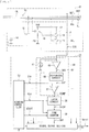
- FIG. 2 illustrates a configuration example of the light source 20 and the light source controller 30. It is to be noted that FIG. 2 also illustrates the controller 12.
- the light source 20 includes a light emitting diode (LED) 21.
- An anode of the light emitting diode (LED) 21 is supplied with a voltage VP, and a cathode of the light emitting diode (LED) 21 is coupled to one end of a current source 33 (described later) of the light source controller 30.
- LED light emitting diode
- the present disclosure is not limited thereto, and a plurality of light emitting diodes may be provided, and the plurality of light emitting diodes may be connected in series, or the plurality of light emitting diodes may be connected in parallel.
- a plurality of light emitting diode groups each including the plurality of light emitting diodes connected in parallel may be provided, and the plurality of light emitting diodes groups may be connected in series.
- the light source controller 30 includes a control signal generator 31, a driver 32, a current source 33, and a switch 34.
- the control signal generator 31 generates control signals S1 and S3 on the basis of an instruction from the controller 12.
- the driver 32 drives the current source 33 on the basis of the control signal S1.
- the current source 33 allows a current having a predetermined current value to flow, and includes, for example, a MOS (Metal Oxide Semiconductor) transistor.
- One end of the current source 33 is coupled to the cathode of the light emitting diode (LED) 21, and the other end is connected to one end of the switch 34.
- the switch 34 performs an on/off operation on the basis of the control signal S3, and includes, for example, a MOS transistor.
- One end of the switch 34 is coupled to the other end of the current source 33, and the other end of the switch 34 is grounded.
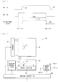
- FIG. 3 illustrates an operation example of the light source 20 and the light source controller 30, where (A) indicates a waveform of the control signal S1, (B) indicates a waveform of the control signal S3, and (C) indicates a waveform of light emitted from the light source 20.
- the control signal S1 when the control signal S1 is in a high level, the current source 33 conducts a current.
- the switch 34 is turned into an on state.
- the light source controller 30 uses the control signals S1 and S3 to control the operation of the light source 20, and the light source 20 emits the light pulse L1.
- this operation will be described in detail.
- control signal generator 31 changes the control signal S3 from a low level to the high level ( FIG. 3 (B) ).
- the switch 34 changes from an off state to the on state.
- the control signal generator 31 changes the control signal S1 from the low level to the high level ( FIG. 3(A) ).
- the driver 32 drives the current source 33 on the basis of the control signal S1.
- the control signal S2 supplied to the current source 33 is, as illustrated in FIG. 3(A) , a dull signal due to the loading, and rises slightly slowly.
- the current source 33 causes a current to flow in response to the control signal S2. This causes the light emitting diode (LED) 21 to begin emitting light ( FIG. 3(C) ).
- the control signal generator 31 changes the control signal S3 from the high level to the low level ( FIG. 3(B) ). This causes the switch 34 to change from the on state to the off state.
- the light emitting diode 21 stops emitting light ( FIG. 3(C) ). As a result, the light source 20 emits the light pulse L1 having a pulse width Tpw as illustrated in FIG. 3(C) .
- the control signal generator 31 changes the control signal S1 from the high level to the low level ( FIG. 3(A) ).
- the driver 32 drives the current source 33 on the basis of the control signal S1.
- the control signal S2 supplied to the current source 33 is a dull signal due to the loading, and falls slightly slowly.
- the light source 20 emits the light pulse L1 ( FIG. 3(C) ) towards the measurement object.
- the switch 34 is provided on the current path of the light emitting diode (LED) 21, it is possible to steepen the change of a light intensity in the posterior end (waveform part WL1) of the light pulse L1 by turning off the switch 34.
- the distance measurement device 1 it is possible to measure the distance D to the measurement object with high accuracy by using the posterior end of the light pulse (reflected light pulse L2) reflected on the measurement object, as will be described later.
- the lens 11 ( FIG. 1 ) forms an image on an imaging plane of the imaging section 40. To the lens 11, the reflected light pulse L2 enters.
- the imaging section 40 acquires a distance image PIC on the basis of an instruction from the controller 12.
- Each of the plurality of pixel values included in the distance image PIC indicates a value of the distance D (distance signal value). Further, the imaging section 40 outputs the acquired distance image PIC as an image signal Spic.
- FIG. 4 illustrates a configuration example of the imaging section 40.
- the imaging section 40 includes a pixel array 41, a scanner 42, a reading section 50, an image generator 44, and an imaging controller 45.
- FIG. 5 illustrates a configuration example of the pixel array 41 and the reading section 50.
- the pixel array 41 is a matrix-like arrangement of a plurality of image pixels P.
- Each of the image pixels P outputs a pixel signal SIG corresponding to the amount of light received.
- the pixel array 41 includes a plurality of control lines TGL, a plurality of control lines RSTL, a plurality of control lines SLL, and a plurality of signal lines SGL.
- the control line TGL extends in a horizontal direction (lateral direction in FIGs 4 and 5 ), and a control signal TG is applied to the control line TGL by the scanner 42.
- the control line RSTL extends in a horizontal direction, and a control signal RST is applied to the control line RSTL by scanner 42.
- the control line RSTL extends in the horizontal direction, and a control signal RST is applied to the control line RSTL by the scanner 42.
- the control line SLL in a horizontal direction, and a control signal SL is applied to the control line SLL by the scanner 42.
- the signal line SGL extends in a vertical direction (longitudinal direction in FIGs 4 and 5 ), and supplies a pixel signal SIG to the reading section 50.
- the image pixel P includes a photodiode 14, a reading transistor 15, a reset transistor 16, a floating diffusion FD, and an output section 17.
- the reading transistor 15 and the reset transistor 16 are each an N-type MOS transistor in this example.
- the photodiode 14 is a photoelectric converter that generates electrons (signal electrons) in accordance with the amount of light received.
- An anode of the photodiode 14 is grounded and a cathode of the photodiode 14 is coupled to a source of the reading transistor 15.
- a gate of the reading transistor 15 is coupled to the control line TGL, the source of the reading transistor 15 is coupled to the cathode of the photodiode 14, and a drain of the reading transistor 15 is coupled to the floating diffusion FD.
- the floating diffusion FD stores the signal electrons supplied by the photodiode 14, and converts the signal electrons into a voltage, and is formed using, for example, a diffusion layer formed on a surface of a semiconductor substrate.
- the floating diffusion FD is illustrated using a symbol of a capacitor element.
- a gate of the reset transistor 16 is coupled to the control line RSTL, a drain of the reset transistor 16 is supplied with a voltage VDD, and a source of the reset transistor 16 is coupled to the floating diffusion FD.
- the output section 17 outputs the voltage corresponding to the number of signal electrons in the floating diffusion FD to the signal line SGL as the pixel signal SIG.
- the output section 17 includes transistors 18 and 19.
- the transistors 18 and 19 are each an N-type MOS transistor in this example.
- a gate of the transistor 18 is coupled to the floating diffusion FD, a drain of the transistor 18 is supplied with the voltage VDD, and a source of the transistor 18 is coupled to a drain of the transistor 19.
- a gate of the transistor 19 is coupled to the control line SLL, the drain of the transistor 19 is coupled to the source of the transistor 18, and a source of the transistor 19 is coupled to the signal line SGL.
- the transistor 19 is turned into the on state on the basis of the control signal SL applied to the control line SLL, whereby the image pixel P is electrically coupled to the signal line SGL. Accordingly, since the transistor 18 is coupled to a current source 61 of the reading section 50 (described later), the transistor 18 operates as a so-called source follower. Further, the reading transistor 15 is turned into the on state on the basis of the control signal TG applied to the control line TGL. The photodiode 14 is thereby coupled to the floating diffusion FD. The gate voltage VG of the reset transistor 16 is set to a middle-level voltage VM on the basis of the control signal RST applied to the control line RSTL.
- the reset transistor 16 causes the reset transistor 16 to be in the intermediate state between the on state and the off state.
- the electrons generated at the photodiode 14 of the image pixel P is supplied to the floating diffusion FD via the reading transistor 15 which is in the on state, the supplied electrons are stored in the floating diffusion FD, and some of the electrons stored in the floating diffusion FD is discharged via the photodiode 14.
- the output section 17 outputs a voltage corresponding to the voltage of the floating diffusion FD to the signal line SGL as the pixel signal SIG. In this manner, the image pixel P supplies the pixel signal SIG to the reading section 50 corresponding to the amount of light received.
- the scanner 42 ( FIG. 4 ) sequentially drives the plurality of image pixels P on a per-pixel line-basis on a basis of an instruction from the imaging controller 45, and includes, for example, a shift register. Specifically, the scanner 42 sequentially drives the plurality of image pixels P on a per-pixel line-basis by applying the control signal TG to the plurality of control lines TGL, applying the control signal RST to the plurality of control lines RSTL, and applying the control signal SL to the plurality of control lines SLL.
- the reading section 50 measures a time interval from a posterior end timing of the light pulse L1 emitted by the light source 20 to a posterior end timing of the reflected light pulse L2 received by the image pixel P on the basis of the pixel signal SIG outputted from the image pixel P. Specifically, the reading section 50 uses the fact that a fall timing (timing t13 in FIG.3 ) of the control signal S3, which is used when the light source 20 emitted the light pulse L1, corresponds to the posterior end timing of the light pulse L1, and the time interval from the fall timing of the control signal S3 to the posterior end timing of the reflected light pulse L2 is measured, thereby measuring the time interval from the posterior end timing of the light pulse L1 to the posterior end timing of the reflected light pulse L2.
- the reading section 50 includes a plurality of reading circuits 60, a signal output section 51, and a reading controller 52.
- the plurality of reading circuits 60 are provided in correspondence with the respective plurality of signal lines SGL in this example, as illustrated in FIG. 5 .
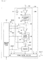
- the reading circuit 60 includes the current source 61, a signal change detector 62, a latch circuit 68, and a time counter 69.
- the current source 61 allows a predetermined current to flow, so that the output section 17 of each image pixel P operates as a source follower.
- the signal change detector 62 detects a signal change corresponding to the posterior end of the reflected light pulse L2 included in the pixel signal SIG.
- the signal change detector 62 includes an amplifier 63, a difference circuit 64, and a comparator 67.
- the amplifier 63 generates a signal S63 by amplifying the pixel signal SIG.
- the gain of the amplifier 63 is able to be about 10 times, for example.
- the difference circuit 64 generates a signal DIF by detecting a difference between signal values at two timings apart from each other by a predetermined time period in the signal S63 outputted from the amplifier 63.
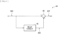
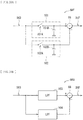
- FIG. 6 illustrates a configuration example of the difference circuit 64.
- the difference circuit 64 includes a delay circuit 65 and a subtracting circuit 66.
- the delay circuit 65 generates a signal S65 by delaying the signal S63 by a predetermined time period.
- the delay circuit 65 includes, for example, a coil and a capacitive element.
- the subtracting circuit 66 generates the signal DIF by subtracting the signal S65 from the signal S63.
- the comparator 67 generates a signal COMP by comparing a voltage of the signal DIF with a threshold voltage Vth.
- a positive input terminal of the comparator 67 is supplied with the signal DIF, and a negative input terminal is supplied with the threshold voltage Vth.
- the latch circuit 68 generates a signal STOP by sampling and latching the signal COMP at a cycle Tclk of a clock signal CLK and holding the sampling result.
- This signal STOP is a signal indicating the posterior end timing of the reflected light pulse L2, as will be described later.
- the time counter 69 performs count operation of counting clock pulses of the clock signal CLK. Specifically, the time counter 69 starts the count operation on the basis of the signal START, and terminates the count operation on the basis of the signal STOP.
- the signal START is a signal indicating the posterior end timing of the light pulse L1 emitted by the light source 20. That is, the count value CNT of the time counter 69 at the time when the count operation ends corresponds to the time interval from the posterior end timing of the light pulse L1 emitted by the light source 20 to the posterior end timing of the reflected light pulse L2 received by the image pixel P. In other words, the count value CNT corresponds to a value (distance signal value) for the distance D in the image pixel P. Then, the time counter 69 supplies the count value CNT to the signal output section 51 after completing the count operation.
- the signal output section 51 sequentially outputs the count values CNT supplied from the plurality of reading circuits 60 as signals Spic1 on the basis of an instruction from the reading controller 52.
- the reading controller 52 controls the read operation in the reading section 50.
- the reading controller 52 also has a function of generating the threshold value voltage Vth, the clock signal CLK, and the signal START.
- the image generator 44 ( FIG. 4 ) generates the distance image PIC in which each pixel value indicating the value of the distance D on the basis of the signal Spic1 supplied from the reading section 50, and outputs the distance image PIC as the image signal Spic.
- the imaging controller 45 supplies the control signal to the scanner 42, the reading section 50, and the image generator 44 on the basis of an instruction from the controller 12, and controls the operation of those circuits, to thereby control the operation of the imaging section 40.
- the imaging section 40 acquires the distance image PIC, and outputs the distance image PIC as the image signal Spic.
- the controller 12 ( FIG. 1 ) supplies the control signal to the light source controller 30 and the imaging section 40, and controls the operation of those circuits, to thereby control the operation of the distance measurement device 1.
- the light source 20 and the light source controller 30 correspond to an example of a "light source section" according to an embodiment of the present disclosure.
- the controller 12 corresponds to an example of a "controller 12" according to an embodiment of the present disclosure.
- the image pixel P corresponds to an example of a "light receiver” according to an embodiment of the present disclosure.
- the light pulse L1 corresponds to an example of a "first light pulse” according to an embodiment of the present disclosure.
- the reflected light pulse L2 corresponds to an example of a "first reflected light pulse” according to an embodiment of the present disclosure.
- the signal change detector 62 corresponds to an example of a "signal change detector” according to an embodiment of the present disclosure.
- the time counter 69 and the reading controller 52 correspond to an example of a "time measurement section" according to an embodiment of the present disclosure.
- the threshold voltage Vth corresponds to an example of a "predetermined threshold” according to an embodiment of the present disclosure.
- the control signal generator 31 corresponds to an example of a "switch controller” according to an embodiment of the present disclosure.
- the reading transistor 15 corresponds to an example of a "first transistor” according to an embodiment of the present disclosure.
- the reset transistor 16 corresponds to an example of a "second transistor” according to an embodiment of the present disclosure.
- the floating diffusion FD corresponds to an example of a "signal converter” according to an embodiment of the present disclosure.
- the scanner 42 corresponds to an example of a "driver” according to an embodiment of the present disclosure.
- the light source controller 30 ( FIG. 1 ) controls the operation of the light source 20 on the basis of an instruction from the controller 12.
- the light source 20 emits the light pulse L1.
- the image pixel P ( FIGs. 4 and 5 ) of the pixel array 41 outputs the pixel signal SIG corresponding to the amount of light received.
- the amplifier 63 ( FIG. 5 ) of the reading section 50 generates the signal S63 by amplifying the pixel signal SIG.
- the difference circuit 64 detects a difference between signal values at two timings apart from each other by a predetermined time period on the basis of the signal S63 outputted from the amplifier 63.
- the comparator 67 generates the signal COMP by comparing the voltage of the signal DIF with the threshold voltage Vth.
- the latch circuit 68 generates a signal STOP by sampling and latching the signal COMP at the cycle Tclk of the clock signal CLK and holding the sampling result.
- the time counter 69 starts the count operation on the basis of the signal START, and terminates the count operation on the basis of the signal STOP. Then, the time counter 69 supplies the count value CNT to the signal output section 51 after completing the count operation.
- the signal output section 51 sequentially outputs the count values CNT supplied from the plurality of reading circuits 60 as signals Spic1.
- the image generator 44 ( FIG. 4 ) then generates the distance image PIC in which each pixel value indicating the value of the distance D on the basis of the signal Spic1, and outputs the distance image PIC as the image signal Spic.
- the imaging section 40 generates the distance image PIC by sequentially driving the plurality of image pixels P in the pixel array 41 on a per-pixel line-basis.
- the scanner 42 changes the control signal SL of the pixel line from the low level to the high level.
- the output section 17 outputs a voltage corresponding to the number of signal electrons in the floating diffusion FD to the signal line SGL as the pixel signal SIG.
- the voltage of the control signal TG maintains the high level.
- the reading transistor 15 thus maintains the on state.
- the voltage of the control signal RST maintains the middle-level voltage VM Accordingly, the reset transistor 16 maintains the intermediate state between the on state and the off state.
- the operation relating to the image pixel P belonging to the pixel line in a case where a certain pixel line is selected will be described in detail.
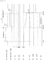
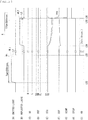
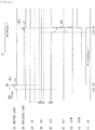
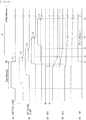
- FIG. 7 illustrates an operation example of the distance measurement device 1, where (A) indicates a waveform of light to be emitted from the light source 20, (B) indicates a waveform of reflected light to be received by the imaging section 40, (C) indicates a waveform of the control signal TG, (D) indicates a waveform of the control signal RST, (E) indicates a waveform of the pixel signal SIG, (F) indicates a waveform of the signal DIF to be outputted from the difference circuit 64, (G) indicates a waveform of the signal COMP to be outputted from the comparator 67, (H) indicates a waveform of the signal STOP to be outputted from the latch circuit 68, and (I) indicates an operation of the time counter 69.
- This example illustrates an operation in a case where a measurement range R is set to about 30 m.
- the time from the light emitted from the light source 20 is reflected by the measurement object to the light is received by the imaging section 40 is about 200 nsec.
- the cycle Tclk of the clock signal CLK is set to 2 nsec.
- the reset transistor 16 maintains the intermediate state between the on state and the off state.
- the resistance value between the drain and the source in reset transistor 16 is higher than resistance value in the on state and lower than the resistance value in the off state.
- the photodiode 14 of the image pixel P In the time period prior to the timing t22, the photodiode 14 of the image pixel P generates an electron by performing photoelectric conversion on the basis of a background light LB.
- the electron is supplied to the floating diffusion FD via the reading transistor 15 which is in the on state and is stored. Since the reset transistor 16 is in the intermediate state between the on state and the off state, some of the electrons stored in the floating diffusion FD is discharged from the floating diffusion FD via reset transistor 16.
- the amount of electrons supplied from the photodiode 14 to the floating diffusion FD according to the background light LB is balanced with the amount of electrons discharged from the floating diffusion FD.
- the voltage of the pixel signal SIG is maintained at voltage V2 slightly lower than voltage V1 ( FIG. 7(E) ), voltage V1 being a voltage in which the background light LB is absent.
- the light source 20 starts emitting light ( FIG. 7(A) ).
- the light source controller 30 drives the light source 20 as illustrated in FIG. 3 on the basis of an instruction from the controller 12, the light source 20 starts emitting light.
- the light source 20 stops emitting light ( FIG. 7(A) ).
- the light source controller 30 drives the light source 20 as illustrated in FIG. 3 on the basis of an instruction from the controller 12, to thereby stop emitting light.
- the light pulse L1 is generated in the time period from timing t22 to timing t23.
- the pulse width Tpw of the light pulse L1 is 200 nsec in this example.
- the time counter 69 starts the count operation ( FIG. 7(I) ). Specifically, first, the controller 12 instructs the reading section 50 to cause the time counter 69 to start the count operation in accordance with the fall timing (timing t13 in FIG. 3 ) of the control signal S3. The reading controller 52 of the reading section 50 generates the signal START at timing t23 corresponding to the posterior end of the light pulse L1 on the basis of an instruction from the controller 12, and the time counter 69 starts the count operation on the basis of the signal START.
- the reflected light pulse L2 corresponding to the light pulse L1 reaches the imaging section 40 ( FIG. 7(B) ).
- the voltage of the pixel signal SIG decreases from voltage V2 ( FIG. 7(E) ).
- the amplifier 63 of the reading circuit 60 amplifies the pixel signal SIG.
- the difference circuit 64 generates the signal DIF on the basis of the signal S63 outputted from the amplifier 63 ( FIG. 7(F) ).
- FIG. 8 illustrates a more specific waveform of the pixel signal SIG and the signal DIF from timing t24 to timing t26.
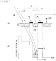
- FIG. 9 illustrates the operation of the image pixel P between timings t24 and t26, where (A) indicates the coupling of the photodiode 14, the reading transistor 15, the floating diffusion FD, and the reset transistor 16, and (B) indicates the electric potentials at the respective elements. Between timings t24 and t26, the photodiode 14 performs photoelectric conversion on the basis of both the background light LB and the reflected light pulse L2. The electrons generated by the photoelectric conversion is stored in the floating diffusion FD. The voltage of the pixel signal SIG is thereby decreased from voltage V2.
- the reset transistor 16 since the reset transistor 16 is in the intermediate state between the on state and the off state, some of the electrons stored in the floating diffusion FD are discharged from the floating diffusion FD via the reset transistor 16. As the electrons stored in the floating diffusion FD increases, the electrons expelled from the floating diffusion FD increases, so that over time, the change in the voltage of the pixel signal SIG becomes gradual.
- the voltage of the pixel signal SIG rises and returns to voltage V2 ( FIG. 7(E) ). That is, since the reflected light pulse L2 terminates at and after timing t26, the electrons supplied to the floating diffusion FD are decreased. As a result, the electrons are discharged from the floating diffusion FD via the reset transistor 16, and the electrons stored in the floating diffusion FD decrease, thereby increasing the voltage of the pixel signal SIG and causing the voltage to return to voltage V2.
- the voltage of the signal DIF outputted from the difference circuit 64 once rises above the threshold voltage Vth and then falls ( FIG. 7(F) ).
- the comparator 67 changes the signal COMP ( FIG. 7(G) ).
- the latch circuit 68 changes the signal STOP from the low level to the high level on the basis of the rising edge of the signal COMP ( FIG. 7(H) ). That is, the change timing of the signal STOP corresponds to the timing of the posterior end (waveform part WL2) of the reflected light pulse L2.
- the part of the pixel signal SIG corresponding to the change timing of the signal STOP is indicated by a circle.
- the time counter 69 then terminates the count operation of the clock signal CLK on the basis of the signal STOP ( FIG. 7(I) ).
- the time counter 69 starts the count operation on the basis of the signal START in the posterior end timing (timing t23) of the light pulse L1 and terminates the count operation on the basis of the signal STOP in the posterior end timing (timing t26) of the reflected light pulse L2. That is, the count value CNT of the time counter 69 when the time counter 69 terminates the count operation corresponds to the time interval from the posterior end timing of the light pulse L1 emitted by the light source 20 to the posterior end timing of the reflected light pulse L2 received by the image pixel P.
- the time counter 69 supplies the count value CNT to the signal output section 51 at and after timing t26.
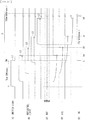
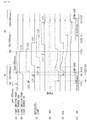
- FIG. 10 illustrates another operation example of the distance measurement device 1.
- This example illustrates an operation in a case where the measurement range R is set to about 120 m.
- the time from the light emitted from the light source 20 is reflected by the measurement object to the light is received by the imaging section 40 is about 800 nsec.
- the cycle Tclk of the clock signal CLK is set to 8 nsec.
- the light source 20 starts emitting light, and at timing t33, the light source 20 stops emitting light ( FIG. 10(A) ).
- the light pulse L1 is generated in the time period from timing t32 to timing t33.
- the time counter 69 starts the count operation ( FIG. 10(I) ).
- the reflected light pulse L2 corresponding to the light pulse L1 reaches the imaging section 40 ( FIG. 10(B) ).
- the voltage of pixel signal SIG decreases from voltage V2 ( FIG. 10(E) ).
- the change in the voltage of the pixel signal SIG from voltage V2 is smaller than a case where the distance D is short (broken line).
- the voltage of the pixel signal SIG rises and returns to voltage V2 ( FIG. 10 (E) ).
- the comparator 67 changes the signal COMP ( FIG. 10(G) ).
- the latch circuit 68 changes the signal STOP from the low level to the high level on the basis of the rising edge of the signal COMP ( FIG. 10(H) ).
- the time counter 69 then terminates the count operation of the clock signal CLK on the basis of the signal STOP ( FIG. 10(I) ).
- the time counter 69 supplies the count value CNT to the signal output section 51 at and after timing t36.
- FIG. 11 illustrates an operation example of the distance measurement device 1 in a case where the distance D between the distance measurement device 1 and the measurement object varies, where (A) indicates a waveform of light to be emitted from the light source 20, (B) indicates waveforms of reflected light to be received by the imaging section 40, (C) indicates a waveform of the control signal RST, (D) indicates waveforms of the pixel signals SIG, and (E) indicates an operation of the time counter 69.
- FIG. 11(E) indicates a time period in which it is possible for the time counter 69 to perform the count operation.
- the timing at which the reflected light pulse L2 reaches the imaging section 40 changes.
- the time counter 69 starts the count operation at timing t1 corresponding to the posterior end of the light pulse L1, and stops the count operation on the basis of the changes of the pixel signals SIG at timings ta, tb, tc, and td corresponding to the posterior ends of the reflected light pulses L2.
- the reading circuit 60 measures the time interval from the posterior end timing of the light pulse L1 emitted by the light source 20 to the posterior end timing of the reflected light pulse L2 received by the image pixel P.
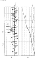
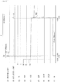
- FIG. 12 illustrates examples of waveforms of the pixel signal SIG and the signal DIF in a case where the distances D between the distance measurement device 1 and the measurement object are distances D1 to D3.
- a waveform SIGD1 indicates a waveform of the pixel signal SIG in a case where the distance D is a distance D1
- a waveform SIGD2 indicates a waveform of the pixel signal SIG in a case where the distance D is a distance D2
- a waveform SIGD3 indicates a waveform of the pixel signal SIG in a case where the distance D is a distance D3.
- a waveform DIFD1 indicates a waveform of the signal DIF in a case where the distance D is the distance D1
- a waveform DIFD2 indicates a waveform of the signal DIF in a case where the distance D is the distance D2
- a waveform DIFD3 indicates a waveform of the signal DIF in a case where the distance D is the distance D3.
- the distance D1 is shorter than the distance D2
- the distance D2 is shorter than the distance D3.
- FIG. 12 the timings at which the pixel signals SIG start to change are drawn to coincide.
- the waveform SIGB of the pixel signal SIG in a case where only the background light LB is used is also depicted.
- the amount of voltage change of the pixel signal SIG varies depending on the distance D between the distance measurement device 1 and the measurement object.
- the voltage of the signal DIF exceeds the threshold voltage Vth. This allows the distance measurement device 1 to generate the signal STOP and the time counter 69 to stop the count operation on the basis of the signal STOP.
- the count value CNT is not changed by the light intensity of the reflected light, it is possible to measure the distance D between the distance measurement device 1 and the measurement object with high accuracy.
- the three cases in which the distances D between the distance measurement device 1 and the measurement object are different are used, but the same applies to, for example, the case in which the reflectances in the measurement object are different.
- the count value CNT does not change depending on the light intensity of the reflected light as described above, so that it is possible to measure the distance D between the distance measurement device 1 and the measurement object with high accuracy.
- the distance measurement device 1 performs an integral action by storing the signal electrons using the floating diffusion FD, and is able to detect a minute signal on the basis of the result obtained by the integral action.
- FIG. 13(A) illustrates an example of an operation in a case where the minute signal is not integrated
- FIG. 13(B) illustrates an example of an operation in a case where the minute signal is integrated
- the background light LB corresponds to a minute signal of 10 electrons
- the reflected light pulse L2 corresponds to a minute signal of 10 electrons.
- the circled portions indicate sample points by the reading circuit 60.
- a noise such as an optical shot noise, for example, is added to the minute signal (signal S11), so that a signal component of the reflected light pulse L2 is buried. Therefore, even if the signal S11 is sampled at the cycle Tclk of the clock signal CLK, there is a possibility that the reflected light pulse L2 is not detected.
- the noise is integrated in addition to the minute signal, so that it is possible to cause the reflected light pulse L2 to be easily detected on the basis of the integrated signal (signal S12). Specifically, it is possible to cause the reflected light pulse L2 to be easily detected by generating a signal S13 corresponding to the signal DIF on the basis of the signal S12 and comparing the voltage of the signal S13 with the threshold voltage Vth.
- the light source 20 emits one light pulse L1, and the image pixel P receives the reflected light pulse L2 corresponding to the light pulse L1.
- a plurality of (e.g., 1000) light pulses can be emitted, and it is possible to make the light intensity (power) of the light pulse L1 higher than the light intensity (power) when the distance D is obtained by performing a statistical process on the basis of the plurality of reflected light pulses corresponding to the plurality of light pulses.
- the distance measurement device 1 since it is possible to reduce the number of light pulses L1 in the distance measurement device 1, it is possible to increase the power per one light pulse L1. As a result, it becomes possible to increase the measurable distance in the distance measurement device 1. For example, by multiplying the power of the light pulse L1 by a factor of 1000, the measurable distance can be extended by a factor of 31.6 (the square root of 1000).
- the light source 20 since the light source 20 emits one light pulse L1, it is possible to reduce the power consumed. That is, for example, in a case where the plurality of light pulses is emitted and the distance D is obtained on the basis of the plurality of reflected light pulses, the power consumed by the circuits that perform the process on the basis of the light source and the plurality of reflected light pulses may be increased. In contrast, in the distance measurement device 1, since the light source 20 emits one light pulse L1 and obtains the distance D on the basis of one reflected light pulse L2, it is possible to reduce the power consumed.
- the voltage of the control signal RST is set to the middle-level voltage VM As a result, it is possible to store the electrons generated in the photodiode 14 in the floating diffusion FD, and to discharge some of the electrons stored in the floating diffusion FD via the reset transistor 16, which enables to increase the measurable distance. That is, if the voltage of the control signal RST is set to the low level voltage VL, since the reset transistor 16 is in the off state, the electrons stored in the floating diffusion FD are not discharged.
- the storage amount of the electrons in the floating diffusion FD may reach the upper limit and become saturated.
- the voltage of the control signal RST is set to the middle-level voltage VM Accordingly, some of the electrons stored in the floating diffusion FD can be discharged via the reset transistor 16, so that the possibility that the electrons based on the background light LB continue to be stored in the floating diffusion FD is be reduced. As a result, it is possible to increase the measurable length in the distance measurement device 1.
- the distance measurement device 1 since the timing of the posterior end of the reflected light pulse L2 is detected, it is possible to easily measure the distance D to the measurement object. That is, as illustrated in FIG. 7 , for example, when the reflected light pulse L2 terminates, since the electrons supplied to the floating diffusion FD decrease, the voltage of the pixel signal SIG rises by discharging the electrons from the floating diffusion FD via the reset transistor 16. As described above, since the pixel signal SIG largely changes at the posterior end timing of the reflected light pulse L2, it is possible to increase an S/N ratio, and thus, it becomes possible to easily detect the timing of the posterior end of the reflected light pulse L2. As a result, the distance measurement device 1 is able to easily measure the distance D to the measurement object.
- the minute signal can be integrated. In this case, in the distance measurement device 1, since it is possible to increase the signal amount by increasing the integration time, it is possible to easily detect the reflected light pulse L2.
- the light source emits one light pulse and the image pixel receives the reflected light pulse corresponding to the light pulse, it is possible to increase the measurable distance
- the light source emits one light pulse and the image pixel receives the reflected light pulse corresponding to the light pulse, it is possible to reduce the power consumed and to cause the device to operate stably.
- the voltage of the control signal RST is set to the middle-level voltage, it is possible to increase the measurable distance,
- the timing of the posterior end of the reflected light pulse is detected, it is possible to easily measure the distances to the measurement object.
- the electrons generated in the photodiode are stored in the floating diffusion, it is possible to easily detect the reflected light pulse.
- the voltage of the control signal RST is set to the middle-level voltage VM, however, as shown in FIG. 14 , this middle-level voltage VM may be adjusted depending on the measurement range R, for example.
- the middle-level voltage VM can be set to three voltages VM1 to VM3. The voltage VM1 is higher than the voltage VM2, and the voltage VM2 is higher than the voltage VM3.
- the middle-level voltage VM to the voltage VM1
- the electric potential difference between the voltage VM1 and the voltage VDD becomes small, so that it is possible to increase the electrons stored in the floating diffusion FD.
- the change of the pixel signal SIG corresponding to the posterior end of the reflected light pulse L2 is slow, because the electrons discharged from the floating diffusion FD are reduced.
- the middle-level voltage VM to the voltage VM3
- the electric potential difference between the voltage VM3 and the voltage VDD becomes large, so that it is possible to increase the electrons discharged from the floating diffusion FD.
- the measurable distance is set to a long distance, for example, it is possible to set the middle-level voltage VM to a high voltage (e.g., voltage VM1).
- a high voltage e.g., voltage VM1
- the measurement resolution may decrease, but since the distance D itself is long, it is possible to suppress the effect on the measurement accuracy.
- the measurable distance is set to a short distance, for example, it is possible to set the middle-level voltage VM to a low voltage (e.g., voltage VM3).
- a low voltage e.g., voltage VM3
- the light intensity of the reflected light pulse L2 is high due to the short distance D, it is possible to increase the electrons stored in the floating diffusion FD to some extent.
- the reset transistor 16 may have a configuration as illustrated in FIG. 15(A) , for example.
- a gate length LL1 of the reset transistor 16 is desirably longer than a gate width WW1 of the reset transistor 16.
- a width WW2 of the floating diffusion FD is desirably wider than the gate width WW1 of the reset transistor 16.
- a width WW3 of a contact region to which the voltage VDD is supplied is desirably wider than the gate width WW1 of the reset transistor 16.
- a length of the source of the reset transistor 16 may be set to a length LL2, and the source may be coupled to the floating diffusion FD.
- a length of the drain of the reset transistor 16 may be set to a length LL3, and the drain may be coupled to the contact region to which the voltage VDD is supplied.
- the resistance value of 100 k ⁇ is, for example, the resistance value when the high level voltage VH is applied to the gate of the reset transistor 16. Further, for example, when the capacitance value is set to 2fF and the resistance value is set to 1 M ⁇ , it is possible to set the time constant to 2 nsec.
- the resistance value of 1 M ⁇ is, for example, the resistance value when the middle-level voltage VM is applied to the gate of the reset transistor 16.
- the light source controller 30 is configured using one current source 33, but the present disclosure is not limited thereto.
- a light source controller 30D according to the present modification example will be described in detail.
- FIG. 16 illustrates a configuration example of the light source controller 30D.
- the light source controller 30D includes a control signal generator 31D, a driver 35, and a current source 36.
- the control signal generator 31D generates control signals S1, S3, and S4 on the basis of an instruction from the controller 12.
- the driver 35 drives the current source 36 on the basis of the control signal S4.
- the current source 36 allows a current of a predetermined current to flow, and has one end coupled to the cathode of the light emitting diode (LED) 21 and the other end coupled to one end of the switch 34. That is, the current source 36 is connected in parallel with the current source 33.
- FIG. 17 illustrates an operation example of the light source 20 and the light source controller 30D, where (A) indicates a waveform the control signal S4, (B) indicates a waveform the control signal S1, (C) indicates a waveform the control signal S3, and (D) indicates a waveform the light to be emitted from the light source 20.
- the control signal S4 when the control signal S4 is in the high level, the current source 36 conducts a current.
- control signal generator 31D changes the control signal S3 from the low level to the high level ( FIG. 17(C) ).
- the switch 34 changes from the off state to the on state.
- the control signal generator 31D changes the control signal S1 from the low level to the high level ( FIG. 17(B) ).
- the driver 32 drives the current source 33 on the basis of the control signal S1.
- the light emitting diode (LED) 21 starts emitting light ( FIG. 17(D) ).
- the control signal generator 31D changes the control signal S4 from the low level to the high level ( FIG. 17(A) ).
- the driver 35 drives the current source 36 on the basis of the control signal S4.
- a current flows through the light emitting diode (LED) 21 to further increase the light intensity ( FIG. 17(D) ).
- the control signal generator 31D changes the control signal S3 from the high level to the low level ( FIG. 17(C) ).
- the switch 34 changes from the on state to the off state.
- the light emitting diode (LED) 21 stops emitting light ( FIG. 17(D) ).
- control signal generator 31D changes the control signals S1 and S4 from the high level to the low level ( FIG. 17(A) and (B) ).
- the light source 20 emits the light pulse L1 ( FIG. 17(D) ) towards the measurement object.
- a distance measurement device 1D including the light source controller 30D since the two current sources 33 and 36 are provided, it is possible to increase the change of the light intensity in the posterior end (waveform part WL1) of the light pulse L1. As a result, it is possible to increase the amount of change of the pixel signal SIG corresponding to the posterior end of the reflected light pulse L2, so that it is possible to increase the measurable distance.
- the current source 36 allows the current to flow only in a predetermined time period in the vicinity of the posterior end of the light pulse L1, it is possible to effectively reduce the power consumed as compared with the case where the current flows in the entire time period from the anterior end to the posterior end of the light pulse L1.
- the image pixel P is provided with four transistors (the reading transistor 15, the reset transistor 16, the transistors 18 and 19) and the floating diffusion FD, but the present disclosure is not limited thereto.
- an imaging section 40E according to the present modification example will be described in detail.
- the imaging section 40E includes a pixel array 41E, a scanner 42E, the reading section 50, the image generator 44, and the imaging controller 45.
- FIG. 18 illustrates a configuration example of the pixel array 41E.
- the pixel array 41E is a matrix-like arrangement of a plurality of image pixels PE.
- the pixel array 41E includes a plurality of control lines RSTL, a plurality of control lines SLL, and a plurality of signal lines SGL.
- the image pixel PE includes a photodiode 14A, the reset transistor 16, and the output section 17.
- the photodiode 14 is replaced with the photodiode 14A, and the reading transistor 15 and the floating diffusion FD are omitted.
- the photodiode 14A is a photoelectric converter that generates electrons (signal electrons) in accordance with the amount of light received and stores the generated electrons therein.
- An anode of the photodiode 14A is grounded and a cathode of the photodiode 14A is coupled to the source of the reset transistor 16 and the gate of the transistor 18.
- the transistor 19 is turned into the on state on the basis of the control signal SL applied to the control line SLL, whereby the image pixel PE is electrically coupled to the signal line SGL. Since the transistor 18 is coupled to the current source 61 of the reading section 50, the transistor 18 operates as a so-called source follower. Further, the gate voltage VG of the reset transistor 16 is set to the middle-level voltage VM on the basis of the control signal RST applied to the control line RSTL. This causes the reset transistor 16 to be in the intermediate state between the on state and the off state.
- the output section 17 outputs a voltage corresponding to the voltage of the cathode of the photodiode 14 to the signal line SGL as the pixel signal SIG.
- the scanner 42E sequentially drives the plurality of image pixels PE on a per-pixel line-basis on a basis of an instruction from the imaging controller 45. Specifically, the scanner 42E applies the control signal RST to the plurality of control lines RSTL, and applies the control signal SL to the plurality of control lines SLL, thereby sequentially driving the plurality of image pixels PE on a per-pixel line-basis.
- FIG. 19 illustrates an operation of the image pixel PE and corresponds to FIG. 9 according to the above embodiment.
- the photodiode 14 performs photoelectric conversion on the basis of both the background light LB and the reflected light pulse L2.
- the electrons generated by the photoelectric conversion are stored in the photodiode 14.
- the reset transistor 16 since the reset transistor 16 is in the intermediate state between the on state and the off state, some of the electrons stored in the photodiode 14 are discharged via the reset transistor 16.
- the output section 17 includes two transistors 18 and 19, but the present disclosure is not limited thereto. Alternatively, for example, the transistor 19 may be omitted. In this case, it is desirable to selectively apply the voltage VDD or the voltage VSS to the drain of the reset transistor 16. In a case where the voltage VDD is applied to the drain of the reset transistor 16, the image pixel is able to output the pixel signal SIG in the similar manner as in the above-described embodiment and the like. In a case where the voltage VSS is applied to the drain of the reset transistor 16, it is possible to turn the transistor 18 into the off state by turning the reset transistor 16 into the on state.
- the difference circuit 64 is configured by the circuit illustrated in FIG. 6 , but the present disclosure is not limited thereto. Alternatively, various configurations may be used that utilize the principles of correlated double sampling (CDS).
- CDS correlated double sampling
- a difference circuit 64F illustrated in FIG. 20A may be used.
- the difference circuit 64F includes sample-hold circuits 101 and 102, and the subtracting circuit 66.
- the sample-hold circuit 101 includes a switch 101A and a capacitive element 101B
- the sample-hold circuit 102 includes a switch 102A and a capacitive element 102B.
- the switches 101A and 102A are turned into the on state at timings different from each other by a predetermined time period.
- the difference circuit 64F is able to generate the signal DIF by detecting a difference between signal values at two timings apart from each other by the predetermined time period in the signal S63.
- the difference circuit 64G includes low-pass filters (LPFs) 103 and 104.
- the low-pass filters (LPFs) 103 and 104 may each include, for example, a resistor and a capacitive element.
- a time constant of the low-pass filter 104 is set to a value longer than a time constant of the low-pass filter 103.
- a phase of the output signal of the low-pass filter (LPF) 104 lags behind a phase of the output signal of the low-pass filter (LPF) 103.
- the difference circuit 64G is able to generate the signal DIF by detecting a difference between signal values at two timings apart from each other by a predetermined time period in the signal S63.
- the difference circuit 64G it is possible to realize a simple configuration as compared with the difference circuit 64F ( FIG. 20A ) in which the switches 101A and 102A are to be turned on and off. Further, in the difference circuit 64G, noises are reduced by the low-pass filters (LPFs) 103 and 104. It is to be noted that, in this example, although two low-pass filters (LPFs) 103 and 104 are provided, the present disclosure is not limited thereto, and for example, the low-pass filter (LPF) 103 may be omitted.
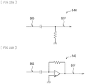
- the difference circuit 64 is used in the above embodiment, the present disclosure is not limited thereto. Instead, a differentiator (Highpass Filter Circuit) 64H illustrated in FIG. 21A or a differentiator 641 illustrated in FIG. 21B may be used.
- the differentiator 64H is a passive type differentiator using a resistor and a capacitive element
- the differentiator 641 is an active type differentiator using a resistor, a capacitive element, and an operational amplifier.
- the differentiators 64H and 641 each output a result of differentiating the signal S63 as the signal DIF.
- the light pulse L1 having a long pulse width Tpw is used, but the present disclosure is not limited thereto.
- a distance measurement device 1J according to the present modification example will be described in detail.
- the distance measurement device 1J has a short measurable distance (e.g., about 3 m).
- the distance measurement device 1J includes the light source 20, a light source controller 30J, the lens 11, the imaging section 40, and the controller 12.
- the light source controller 30J controls the operation of the light source 20 on the basis of an instruction from the controller 12.
- the light source controller 30J includes a control signal generator 31J, the driver 32, the current source 33, and the switch 34.
- the control signal generator 31J generates the control signals S1 and S3 such that the light source 20 emits the light pulse L1 having a short pulse width Tpw.
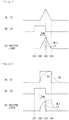
- FIG. 22 illustrates an operation example of the light source 20 and a light source controller 30J.
- the control signal generator 31J generates the control signal S1 in a form of a triangular waveform.
- the control signal generator 31J changes the control signal S3 from the low level to the high level ( FIG. 22(B) ).
- the switch 34 changes from the off state to the on state.
- the control signal generator 31J gradually changes the control signal S1 from the low level to the high level ( FIG. 22(A) ).
- the driver 32 drives the current source 33 on the basis of the control signal S1.
- the light emitting diode (LED) 21 starts emitting light and gradually increases the light intensity ( FIG. 22(C) ).
- the control signal generator 31J changes the control signal S3 from the high level to the low level ( FIG. 22(B) ).
- the switch 34 changes from the on state to the off state.
- the light emitting diode (LED) 21 stops emitting light ( FIG. 22(C) ).
- the control signal generator 31J gradually changes the control signal S1 from the high level to the low level ( FIG. 22(A) ).
- FIG. 23 illustrates another operation example of the light source 20 and the light source controller 30J.
- the control signal generator 31J generates the control signal S1 in a form of a rectangular waveform.
- the control signal generator 31J changes the control signal S3 from the low level to the high level ( FIG. 23(B) ).
- the switch 34 changes from the off state to the on state.
- the control signal generator 31J changes the control signal S1 from the low level to the high level ( FIG. 23(A) ).
- the driver 32 drives the current source 33 on the basis of the control signal S1.
- the control signal S2 supplied to the current source 33 becomes a dull signal due to loading and rises slightly slowly.
- the current source 33 causes a current to flow in response to the control signal S2.
- the light emitting diode (LED) 21 starts emitting light ( FIG. 23(C) ).
- the control signal generator 31J changes the control signal S3 from the high level to the low level ( FIG. 23(B) ).
- the switch 34 changes from the on state to the off state.
- the light emitting diode (LED) 21 stops emitting light ( FIG. 23(C) ).
- the control signal generator 31J changes the control signal S1 from the high level to the low level ( FIG. 23(A) ).
- the driver 32 drives the current source 33 on the basis of the control signal S1.
- the control signal S2 supplied to the current source 33 becomes a dull signal due to loading and falls slightly slowly.
- the light source 20 emits the light pulse L1 having a short pulse width Tpw ( FIGs. 22(C) and 23(C) ) towards the measurement object. Also in the distance measurement device 1J, by turning off the switch 34, the change of the light intensity in the posterior end (waveform part WL1) of the light pulse L1 is made steep.
- FIG. 24 illustrates an operation example of the distance measurement device 1J.
- the example illustrates an operation in a case where the measurement range R is set to about 3m.
- the time from the light emitted from the light source 20 is reflected by the measurement object to the light is received by the imaging section 40 is about 20 nsec.
- the cycle Tclk of clock signal CLK is set to 200 psec.
- the amount of electrons supplied from the photodiode 14 to the floating diffusion FD according to the background light LB is balanced with the amount of electrons discharged from the floating diffusion FD.
- the voltage of the pixel signal SIG is maintained at voltage V2 ( FIG. 24(E) ).
- the light source 20 starts emitting light, and the light intensity gradually increases in the time period from timing t72 to timing t73 ( FIG. 24(A) ). Then, at timing t73, the light source 20 stops emitting light. As a result, the light pulse L1 is generated in the time period from timing t72 to timing t73.
- the pulse width Tpw of the light pulse L1 is, in this example, 2 nsec.
- the time counter 69 starts the count operation ( FIG. 24 (I) ).
- the reflected light pulse L2 corresponding to the light pulse L1 reaches the imaging section 40 ( FIG. 24(B) ).
- the voltage of the pixel signal SIG decreases from voltage V2 in the time period from timing t74 to timing t75 ( FIG. 24(E) ).
- the amplifier 63 of the reading circuit 60 amplifies the pixel signal SIG.
- the difference circuit 64 generates the signal DIF on the basis of the signal S63 outputted from the amplifier 63 ( FIG. 24(F) ).
- the voltage of the pixel signal SIG rises and returns to voltage V2 ( FIG. 24(E) ).
- the voltage of the signal DIF outputted from the difference circuit 64 rises once, exceeds the threshold voltage Vth, and then falls ( FIG. 24(F) ).
- the comparator 67 changes the signal COMP ( FIG. 24(G) ).
- the latch circuit 68 changes the signal STOP from the low level to the high level on the basis of the rising edge of the signal COMP ( FIG. 24(H) ).
- the time counter 69 terminates the count operation of the clock signal CLK on the basis of the signal STOP ( FIG. 24(I) ).
- the time counter 69 supplies the count value CNT to the signal output section 51 at and after timing t75.
- the distance measurement device 1J by using the light pulse L1 having a short pulse width Tpw, for example, it is possible to measure a short distance D while reducing power consumption.
- the image pixel P is arranged in the form of matrices in the plane, but the present disclosure is not limited thereto.
- a so-called line sensor may be configured by arranging image pixels P in one row, for example. Further, for example, a single image pixel P may be provided.
- the photodiode 14 of the image pixel P may be, for example, an avalanche photodiode. Further, for example, the amplifier 63 may be omitted in the reading circuit 60.
- the measurable distance is extended by storing more electrons in the floating diffusion FD.
- the components substantially the same as those of the distance measurement device 1 according to the first embodiment are denoted by the same reference numerals, and descriptions thereof are omitted as appropriate.
- the distance measurement device 2 includes the light source 20, the light source controller 30, the lens 11, an imaging section 70, and the controller 12.
- the imaging section 70 includes the pixel array 41, a scanner 72, the reading section 50, the image generator 44, and the imaging controller 45.
- the scanner 72 sequentially drives the plurality of image pixels P on a per-pixel line-basis on the basis of an instruction from the imaging controller 45.
- the scanner 72 alternates the voltage of the control signal RST between the middle-level voltage VM and the low level voltage VL in the time period corresponding to the second half of the measurement range R.
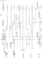
- FIG. 25 illustrates an operation example of the distance measurement device 2, where (A) indicates a waveform of light to be emitted from the light source 20, (B) indicates a waveform of reflected light to be received by the imaging section 70, (C) indicates a waveform of the control signal TG, (D) indicates a waveform of the control signal RST to be generated by the scanner 42, (E) indicates a waveform of the gate voltage VG of the reset transistor 16, (F) indicates a waveform of the pixel signal SIG, (G) indicates a waveform of the signal DIF to be outputted from the difference circuit 64, (H) indicates a waveform of the signal COMP to be outputted from the comparator 67, (I) indicates a waveform of the signal STOP to be outputted from the latch circuit 68, and (J) indicates an operation of the time counter 69.
- This example illustrates an operation in a case where a measurement range R is set to about 300 m.
- the distance D between the distance measurement device 2 and the measurement object is 300 m
- the time from the light emitted from the light source 20 is reflected by the measurement object to the light is received by the imaging section 40 is about 2000 nsec.
- the cycle Tclk of the clock signal CLK is set to 20 nsec.
- the amount of electrons supplied from the photodiode 14 to the floating diffusion FD according to the background light LB is balanced with the amount of electrons discharged from the floating diffusion FD.
- the voltage of the pixel signal SIG is maintained at voltage V2 ( FIG. 25(F) ).
- the light source 20 starts emitting light, and at timing t84, the light source 20 stops emitting light ( FIG. 25(A) ).
- the light pulse L1 is generated in the time period from timing t82 to timing t84.
- the pulse width Tpw of the light pulse L1 is 2000 nsec in this example.
- the time counter 69 starts the count operation ( FIG. 25(J) ).
- the reflected light pulse L2 corresponding to the light pulse L1 reaches the imaging section 70 ( FIG. 25(B) ).
- the voltage of pixel signal SIG decreases from voltage V2 ( FIG. 25F ).
- the amplifier 63 of the reading circuit 60 amplifies the pixel signal SIG.
- the difference circuit 64 generates the signal DIF on the basis of the signal S63 outputted from the amplifier 63 ( FIG. 25(G) ).
- the voltage of the control signal RST regarding the image pixel P is alternated between the middle-level voltage VM and the low level voltage VL ( FIG. 25(D) ).
- the alternating cycle may be set to, for example, 20 nsec. as in the cycle Tclk of clock signal CLK. This causes the gate voltage VG of the reset transistor 16 to alternate between the middle-level voltage VM and the low level voltage VL with a slight slowing down ( FIG. 25(E) ).
- timing t85 is the timing at which the distance D between distance measurement device 2 and measurement object corresponds to 150 m
- timing t87 is the timing at which the distance D between distance measurement device 2 and measurement object corresponds to 300 m. That is, the scanner 72 alternates the voltage of the control signal RST between the middle-level voltage VM and the low level voltage VL in the time period corresponding to the second half of the measurement range R.
- the voltage of the pixel signal SIG rises and returns to voltage V2 ( FIG. 25(F) ).
- the voltage of the signal DIF outputted from the difference circuit 64 rises once, exceeds the threshold voltage Vth G, and then falls ( FIG. 25(G) ).
- the comparator 67 changes the signal COMP ( FIG. 25(H) ).
- the latch circuit 68 changes the signal STOP from the low level to the high level on the basis of the rising edge of the signal COMP, ( FIG. 25(I) ).
- the time counter 69 terminates the count operation of the clock signal CLK on the basis of the signal STOP at timing t86 corresponding to the posterior end (waveform part WL2) of the reflected light pulse L2 ( FIG. 25(J) ).
- the time counter 69 supplies the count value CNT to the signal output section 51 at and after timing t86.
- the voltage of the control signal RST is alternated between the middle-level voltage VM and the low level voltage VL.
- the voltage of control signal RST is alternated between the middle-level voltage VM and the low level voltage VL to increase the electrons stored in the floating diffusion FD.
- the distance measurement device 2 it is possible to increase the amount of change of the pixel signal SIG corresponding to the posterior end (waveform part WL2) of the reflected light pulse L2, so that it is possible to increase the measurable distance. For example, by multiplying the quantity of electrons stored in the floating diffusion FD by a factor of 10, the measurable distance can be extended by a factor of 3.16 (the square root of 10).
- the alternating cycle of the control signal RST in the second half of the measurement range R is set to the same level as the cycle Tclk of the clock signal CLK, it is possible to suppress the deterioration of the measurement resolution. That is, when the gate voltage VG of the reset transistor 16 comes near the low level voltage VL, electrons are stored in the floating diffusion FD, but the electrons are not discharged from the floating diffusion FD. Therefore, when the gate voltage VG of the reset transistor 16 comes near the low level voltage VL at the timing at which the reflected light pulse L2 terminates, the amount of change of the pixel signal SIG is small, so that the signal DIF hardly exceeds the threshold voltage Vth.
- control signal RST is made comparable to the cycle Tclk of the clock signal CLK.
- the distance measurement device 2 since it is possible to make the measurement resolution determined by the cycle Tclk of the clock signal CLK and the measurement resolution determined by the alternating cycle of the control signal RST substantially the same, it is possible to suppress the deterioration of the measurement resolution due to the alternating of the control signal RST.
- the modification examples of the first embodiment may be applied to the distance measurement device 2 according to the above embodiment.
- a distance measurement device 3 according to a third embodiment will be described.
- the electrons are not discharged from the floating diffusion FD.
- the components substantially the same as those of the distance measurement device 1 according to the first embodiment are denoted by the same reference numerals, and descriptions thereof are omitted as appropriate.
- the distance measurement device 3 includes the light source 20, the light source controller 30, the lens 11, an imaging section 80, and the controller 12.
- the imaging section 80 includes the pixel array 41, a scanner 82, the reading section 50, the image generator 44, and the imaging controller 45.
- the scanner 82 sequentially drives the plurality of image pixels P on a per-pixel line-basis on the basis of an instruction from the imaging controller 45.
- the scanner 82 applies the control signal RST having the high level voltage VH or the low level voltage VL to the plurality of control lines RSTL.
- FIG. 26 illustrates an operation example of the distance measurement device 3, where (A) indicates a waveform of light to be emitted from the light source 20, (B) indicates a waveform of reflected light to be received by the imaging section 80, (C) indicates a waveform of the control signal TG, (D) indicates a waveform of the control signal RST, (E) indicates a waveform of the pixel signal SIG, (F) indicates a waveform of the signal DIF to be outputted from the difference circuit 64, (G) indicates a waveform of the signal COMP to be outputted from the comparator 67, (H) indicates a waveform of the signal STOP to be outputted from the latch circuit 68, and (I) indicates an operation of the time counter 69.
- This example illustrates an operation in a case where a measurement range R is set to about 30 m.
- the time from the light emitted from the light source 20 is reflected by the measurement object to the light is received by the imaging section 40 is about 200 nsec.
- the cycle Tclk of the clock signal CLK is set to 2 nsec.
- the scanner 82 of the imaging section 80 changes the voltage of the control signal RST regarding the image pixel P from the high level voltage VH to the low level voltage VL ( FIG. 26(D) ).
- the reset transistor 16 of the image pixel P turns into the off state.
- the voltage of the control signal RST changes, the voltage of the pixel signal SIG slightly drops and becomes voltage V3 ( FIG. 26(E) ).
- the voltage of the pixel signal SIG gradually decreases from voltage V3 at and after timing t91. That is, the photodiode 14 generates electrons by performing photoelectric conversion on the basis of the background light LB, and the electrons are stored in the floating diffusion FD, so that the voltage of the pixel signal SIG gradually decreases.
- the voltage of the control signal RST is set to the low level voltage VL before the light source 20 starts emitting the light pulse L1, but the present disclosure is not limited thereto.
- the voltage of the control signal RST may be set to the low level voltage VL after the light source 20 starts emitting the light pulse L1, as described below.
- the light source 20 starts emitting light, and at timing t93, the light source 20 stops emitting light ( FIG. 26(A) ).
- the light pulse L1 is generated in the time period from timing t92 to timing t93.
- the pulse width Tpw of this light pulse L1 is 200 nsec in this example.
- the time counter 69 starts the count operation ( FIG. 26(I) ).
- the reflected light pulse L2 corresponding to the light pulse L1 reaches the imaging section 80 ( FIG. 26(B) ).
- the voltage of the pixel signal SIG is further reduced by a larger degree of change ( FIG. 26(E) ).
- the amplifier 63 of the reading circuit 60 amplifies the pixel signal SIG.
- the difference circuit 64 generates the signal DIF on the basis of the signal S63 outputted from the amplifier 63 ( FIG. 26(F) ).
- FIG. 27 illustrates the operation of the image pixel P between timings t94 and t96, where (A) indicates the coupling of the photodiode 14, the reading transistor 15, the floating diffusion FD, and the reset transistor 16, and (B) indicates the electric potentials at the respective elements.
- the photodiode 14 performs photoelectric conversion on the basis of both the background light LB and the reflected light pulse L2.
- the electrons generated by the photoelectric conversion is stored in the floating diffusion FD.
- the reset transistor 16 since the reset transistor 16 is in the off state, the electrons stored in the floating diffusion FD are not discharged via the reset transistor 16, unlike the case of the distance measurement device 1 according to the first embodiment, for example.
- the voltage of the pixel signal SIG continues to drop, because the electrons continue to be stored in the floating diffusion FD.
- the voltage of the signal DIF outputted from the difference circuit 64 rises once, exceeds the threshold voltage Vth, and then falls ( FIG. 26(F) ).
- the comparator 67 changes the signal COMP ( FIG. 26(G) ).
- the latch circuit 68 changes the signal STOP from the low level to the high level on the basis of the rising edge of the signal COMP ( FIG. 26(H) ). That is, the change timing of the signal STOP corresponds to the timing of the posterior end (waveform part WL2) of the reflected light pulse L2.
- the time counter 69 terminates the count operation of the clock signal CLK on the basis of the signal STOP ( FIG. 26(I) ).
- the time counter 69 supplies the count value CNT to the signal output section 51 at and after timing t96.
- FIG. 28 illustrates an operation example of the distance measurement device 3 where the distance D between the distance measurement device 3 and the measurement object varies, where (A) indicates a waveform of light to be emitted from the light source 20, (B) indicates waveforms of reflected light to be received by the imaging section 80, (C) indicates a waveform of the control signal RST, (D) indicates waveforms of the pixel signals SIG, (E) indicates an operation of the time counter 69.
- FIG. 28(E) illustrates a time period in which the time counter 69 is able to perform the count operation.
- the voltage of the control signal RST is turned to the low level voltage VL after the light source 20 starts emitting the light pulse L1.
- the measurement range R is set to about 120 m.
- the cycle Tclk of the clock signal CLK is set to 8 nsec.
- the timing at which the reflected light pulse L2 reaches the imaging section 80 changes in accordance with the distance D between the distance measurement device 3 and the measurement object.
- the time counter 69 starts the count operation at timing t1 corresponding to the posterior end of the light pulse L1, and stops the count operation on the basis of the changes of the pixel signals SIG at timings ta, tb, tc, and td corresponding to the posterior ends of the reflected light pulses L2.
- the reading circuit 60 measures the time interval from the time the light source 20 emits the light pulse L1 to the time the image pixel P receives the reflected light pulse L2.
- control signal RST is set to the low level voltage VL and the electrons are not discharged from the floating diffusion FD, it is possible to measure the distance D between the distance measurement device 3 and the measurement object.
- the light pulse L1 having a long pulse width Tpw is used, but the present disclosure is not limited thereto.
- a distance measurement device 3A according to the present modification example will be described in detail.
- the distance measurement device 3A has a short measurable distance (e.g., about 3 m).
- the distance measurement device 3A includes a light source 20A, a light source controller 30A, the lens 11, an imaging section 80A, and the controller 12.
- the light source 20A includes a laser device. That is, in this example, the light pulse L1 is a laser beam.
- the light source controller 30A controls the operation of the light source 20A on the basis of an instruction from the controller 12.
- the imaging section 80A includes the pixel array 41, the scanner 82, a reading section 50A, the image generator 44, and the imaging controller 45.
- FIG. 29 illustrates a configuration example of the reading section 50A.
- the reading section 50A includes a plurality of reading circuits 60A.
- the reading circuit 60A includes a signal change detector 62A.
- the signal change detector 62A includes a differentiator 64A.
- the differentiator 64A the differentiator 64H illustrated in FIG. 21A or the differentiator 64I illustrated in FIG. 21B may be used.
- FIG. 30 illustrates an operation example of the distance measurement device 3A.
- the example illustrates an operation in a case where the measurement range R is set to about 3m.
- the time from the light emitted from the light source 20 is reflected by the measurement object to the light is received by the imaging section 40 is about 20 nsec.
- the cycle Tclk of clock signal CLK is set to 200 psec.
- the scanner 82 of the imaging section 80A changes the voltage of the control signal RST regarding the image pixel P from the high level voltage VH to the low level voltage VL ( FIG. 30(D) ).
- the voltage of the control signal RST changes, the voltage of the pixel signal SIG slightly drops and becomes voltage V3 ( FIG. 30(E) ).
- the voltage of the pixel signal SIG gradually decreases from voltage V3 at and after timing t101, due to the effect of the background light LB.
- the light source 20A starts emitting light, and the light intensity gradually increases in the time period from timing t102 to timing t103 ( FIG. 30(A) ).
- the light source 20A stops emitting light.
- the light pulse L1 is generated in the time period from timing t102 to timing t103.
- the pulse width Tpw of the light pulse L1 is 200 psec or less in this example.
- the time counter 69 starts the count operation ( FIG. 30(I) ).
- the reflected light pulse L2 corresponding to the light pulse L1 reaches the imaging section 80 at timing t104 ( FIG. 30(B) ).
- the voltage of the pixel signal SIG is further reduced with a greater degree of change ( FIG. 30(E) ).
- the amplifier 63 of the reading circuit 60A amplifies the pixel signal SIG.
- the differentiator 64A generates the signal DIF on the basis of the signal S63 outputted from the amplifier 63 ( FIG. 30(F) ).
- the degree of change of the voltage of the pixel signal SIG decreases ( FIG. 30(E) ).
- the voltage of the signal DIF outputted from the differentiator 64A drops once and then rises, exceeds the threshold voltage Vth, and then falls ( FIG. 30(F) ).
- the comparator 67 changes the signal COMP ( FIG. 30(G) ).
- the latch circuit 68 changes the signal STOP from the low level to the high level on the basis of the rising edge of the signal COMP ( FIG. 30(H) ). That is, the change timing of the signal STOP corresponds to the posterior end timing of the reflected light pulse L2.
- the time counter 69 terminates the count operation of the clock signal CLK on the basis of the signal STOP at timing t105 ( FIG. 30(I) ).
- the time counter 69 supplies the count value CNT to the signal output section 51 at and after timing t105.
- the light source 20A since the light source 20A includes the laser device, it is possible to decrease the pulse width Tpw of the light pulse L1 and to increase the light intensity of the light pulse L1. This makes it possible to increase the measurable distance in the distance measurement device 3A.
- the signal electrons are stored in the floating diffusion FD while the light intensity of the light pulse L1 is increased in this manner, it is possible to increase the S/N ratio, which allows the timing of posterior end of the reflected light pulse L2 to be detected easily.
- the modification examples of the first embodiment may be applied to the distance measurement device 3 according to the above embodiment.
- a distance measurement device 4 according to a fourth embodiment will be described.
- two light pulses are emitted, and the distance D is obtained on the basis of two reflected light pulses corresponding to the two light pulses.
- the components substantially the same as those of the distance measurement device 1 according to the first embodiment are denoted by the same reference numerals, and descriptions thereof are omitted as appropriate.
- FIG. 31 illustrates a configuration example of the distance measurement device 4.
- the distance measurement device 4 includes a light source 90, a light source controller 100, the lens 11, an imaging section 110, and the controller 12.
- the light source 90 emits two light pulses L11 and L12 toward the measurement object, and includes, for example, a light emitting diode.
- the light pulse L11 is a pulse whose pulse width Tpwl is short
- the light pulse L12 is a pulse whose pulse width Tpwl is long.
- the light source controller 100 controls the operation of the light source 90 on the basis of an instruction from the controller 12.
- the lens 11 forms an image on an imaging plane of the imaging section 110.
- two reflected light pulses L21 and L22 respectively corresponding to the two light pulses L11 and L12 enter.
- the imaging section 110 acquires the distance image PIC on the basis of an instruction from the controller 12.
- the imaging section 110 includes the pixel array 41, the scanner 42, a reading section 120, the image generator 44, and the imaging controller 45.
- the reading section 120 has a plurality of reading circuits 130.
- the distance measurement device 4 measures the distance D using the light pulse L11 having the short pulse width Tpwl and the reflected light pulse L21, and, in the case where the distance D from the distance measurement device 4 to the measurement object is long, the distance measurement device 4 measures the distance D using the light pulse L12 having the long pulse width Tpw2 and the reflected light pulse L22.
- the light pulse L11 corresponds to an example of a "first light pulse” according to an embodiment of the present disclosure.
- the light pulse L12 corresponds to an example of a “second light pulse” according to an embodiment of the present disclosure.
- the reflected light pulse L21 corresponds to an example of a "first reflected light pulse” according to an embodiment of the present disclosure.
- the reflected light pulse L22 corresponds to an example of a "second reflected light pulse” according to an embodiment of the present disclosure.
- the reading controller 52 corresponds to an example of a "clock generator” according to an embodiment of the present disclosure.
- FIG. 32 illustrates an operation example of the distance measurement device 4 in a case where the distance D between the distance measurement device 4 and the measurement object varies, where (A) indicates a waveform of light to be emitted from the light source 90, (B) indicates waveforms of reflected light to be received by the imaging section 110, (C) indicates a waveform of the control signal RST, (D) indicates waveforms of the pixel signals SIG, and (E) indicates an operation of the time counter 69.
- FIG. 32(E) indicates a time period in which it is possible for the time counter 69 to perform the count operation.
- the measurement range R is set to about 120 m.
- the measurement range R includes a measurement range R1 for short distances from 0 m to 15 m and a measurement range R2 for long distances from 15 m to 120 m.
- the measurement range R1 for short distances is a range in which the distance D is measured using the light pulse L11 having the short pulse width Tpwl and the reflected light pulse L21
- the measurement range R2 for long distances is a range in which the distance D is measured using the light pulse L12 having the long pulse width Tpw2 and the reflected light pulse L22.
- the cycle Tclk of the clock signal CLK is set to 1 nsec, and, in the measurement range R2 for long distances, the cycle Tclk of the clock signal CLK is set to 8 nsec.
- the light source 90 sequentially emits the light pulse L11 and the light pulse L12 in this order.
- the pulse width Tpwl of the light pulse L11 is 2 nsec and the pulse width Tpw2 of the light pulse L12 is 200 nsec.
- the imaging section 110 successively receives the reflected light pulse L21 and the reflected light pulse L22.
- the timings at which the reflected light pulses L21 and L22 reaches the imaging section 110 vary.
- the time counter 69 starts the count operation at timing t111 corresponding to the posterior end of the light pulse L11.
- the cycle Tclk of the clock signal CLK at this time is 1 nsec.
- the time counter 69 stops the count operation on the basis of the change in the pixel signal SIG at a timing corresponding to the posterior end of the reflected light pulse L21 (timings ta and tb in this example).
- the specific operation is similar to the operation of the distance measurement device 1J ( FIG. 24 ).
- the reading circuit 130 measures the time interval from the posterior end timing of the light pulse L11 emitted by the light source 90 to the posterior end timing of the reflected light pulse L21 received by the image pixel P.
- the time counter 69 temporarily stops the count operation at timing t112. At this time, the count value CNT is 100. The time counter 69 then resumes the count operation at timing t114, which is 100 nsec later than timing t113 corresponding to the posterior end of the light pulse L12. That is, the count value CNT is counted up from 100.
- the cycle Tclk of the clock signal CLK at this time is 8 nsec.
- the time counter 69 stops the count operation on the basis of the change of the pixel signal SIG at a timing corresponding to the posterior end of the reflected light pulse L22 (timings tc and td in this example).
- the specific operation is similar to the operation of the distance measurement device 1 ( FIG. 7 ).
- the count value CNT is 188.
- the reading circuit 130 measures the time interval from timing t114, which is 100 nsec later than the posterior end timing of the light pulse L12 emitted by the light source 90 to the posterior end timing of the reflected light pulse L22 received by the image pixel P.
- the reading circuit 130 equivalently measure the time interval from the posterior end timing of the light pulse L12 emitted by the light source 90 to the posterior end timing of the reflected light pulse L22 received by the image pixel P.
- the measurement range R is divided into the measurement range R1 for short distances and the measurement range R2 for long distances. Then, in the measurement range R1 for short distances, the distance D is measured by using the light pulse L11 having the short pulse width Tpwl and the reflected light pulse L21, and in the measurement range R2 for long distances, the distance D is measured by using the light pulse L12 having the long pulse width Tpw2 and the reflected light pulse L22. Further, the cycle Tclk of the clock signal CLK at the time of performing the measurement in the measurement range R2 for long distances is made longer than the cycle Tclk of the clock signal CLK at the time of performing the measurement in the measurement range R1 for short distances.
- the distance measurement device 4 it is possible to increase the measurement resolution in a case where the distance D is short, as compared with a case where the cycle Tclk of the clock signal CLK is constant in the whole range of the measurement range R, for example. Further, for example, in a case where the distance D is long (e.g., 120 m), it is possible to suppress the count value CNT of the time counter 69 to a low value, which enables to suppress the circuit size of the time counter 69. In addition, in the case where the distance D is long, it is possible to lower a frequency of the clock signal CLK, which enables to reduce the power consumption.
- the measurement range R is divided into the measurement range R1 for short distances and the measurement range R2 for long distances, but the present disclosure is not limited thereto, and instead, the measurement range R may be divided into, for example, three or more measurement ranges.
- the modification examples of the first embodiment may be applied to the distance measurement device 4 according to the above embodiment.
- a distance measurement device 5 according to a fifth embodiment will be described.
- two light pulses are respectively emitted two light sources.
- the components substantially the same as those of the distance measurement device 4 according to the fourth embodiment are denoted by the same reference numerals, and descriptions thereof are omitted as appropriate.
- FIG. 33 illustrates a configuration example of the distance measurement device 5.
- the distance measurement device 5 includes the light sources 20A and 20, a light source controller 140, the lens 11, an imaging section 150, and the controller 12.
- the light source 20A emits the light pulse L11 toward the measurement object, and includes a laser device.
- the light source 20 emits the light pulse L12 toward the measurement object, and includes a light emitting diode.
- the light pulse L11 is a pulse with a short pulse width Tpwl
- the light pulse L12 is a pulse with a long pulse width Tpw2.
- the light source controller 140 controls the operations of the light sources 20A and 20 on the basis of an instruction from the controller 12.
- the lens 11 forms an image on an imaging plane of the imaging section 150.
- two reflected light pulses L21 and L22 respectively corresponding to the two light pulses L11 and L12 enter.
- the imaging section 150 acquires the distance image PIC on the basis of an instruction from the controller 12.
- the imaging section 150 includes the pixel array 41, the scanner 42, a reading section 160, the image generator 44, and the imaging controller 45.
- the reading section 160 includes a plurality of reading circuits 170.
- the distance measurement device 5 measures the distance D using the light pulse L11 having the short pulse width Tpwl and the reflected light pulse L21, and, in the case where the distance D from the distance measurement device 5 to the measurement object is long, the distance measurement device 5 measures the distance D using the light pulse L12 having the long pulse width Tpw2 and the reflected light pulse L22.
- FIG. 34 illustrates an operation example of the distance measurement device 5 in a case where the distance D between the distance measurement device 5 and the measurement object varies, where (A) indicates a waveform of light to be emitted from the light source 20A, (B) indicates a waveform of light to be emitted from the light source 20, (C) indicates waveforms of reflected light to be received by the imaging section 150, (D) indicates a waveform of the control signal RST, (E) waveforms of the pixel signals SIG, and (F) indicates an operation of the time counter 69.
- FIG. 34(F) indicates a time period in which it is possible for the time counter 69 to perform the count operation.
- the measurement range R is set to about 120 m.
- the measurement range R includes a measurement range R1 for short distances from 0 m to 15 m and a measurement range R2 for long distances from 15 m to 120 m.
- the measurement range R1 for short distances is a range in which the distance D is measured using the light pulse L11 having the short pulse width Tpwl and the reflected light pulse L21
- the measurement range R2 for long distances is a range in which the distance D is measured using the light pulse L12 having the long pulse width Tpw2 and the reflected light pulse L22.
- the cycle Tclk of the clock signal CLK is set to 200 psec, and, in the measurement range R2 for long distances, the cycle Tclk of the clock signal CLK is set to 8 nsec.
- the light source 20A emits the light pulse L11, and then the light source 20 emits the light pulse L12.
- the pulse width Tpwl of the light pulse L11 is 200 psec and the pulse width Tpw2 of the light pulse L12 is 700 nsec.
- the imaging section 150 successively receives the reflected light pulse L21 and the reflected light pulse L22.
- the timings at which the reflected light pulses L21 and L22 reaches the imaging section 150 vary.
- the time counter 69 starts the count operation at timing t111 corresponding to the posterior end of the light pulse L11.
- the cycle Tclk of the clock signal CLK at this time is 200 psec.
- the time counter 69 stops the count operation on the basis of the change in the pixel signal SIG at a timing corresponding to the posterior end of the reflected light pulse L21 (timings ta and tb in this example).
- the specific operation is similar to the operation of the distance measurement device 3A ( FIG. 30 ).
- the reading circuit 170 measures the time interval from the posterior end timing of the light pulse L11 emitted by the light source 20A to the posterior end timing of the reflected light pulse L21 received by the image pixel P.
- the time counter 69 temporarily stops the count operation at timing t122.
- the count value CNT is 500.
- the imaging section 150 sets the control signal RST to the high level voltage VH and then to the middle-level voltage VM
- the time counter 69 then resumes the count operation at timing t126, which is 100 nsec later than timing t125 corresponding to the posterior end of the light pulse L12. That is, the count value CNT is counted up from 500.
- the cycle Tclk of the clock signal CLK at this time is 8 nsec.
- the time counter 69 stops the count operation on the basis of the change of the pixel signal SIG at a timing corresponding to the posterior end of the reflected light pulse L22 (timings tc and td in this example).
- the specific operation is similar to the operation of the distance measurement device 1 ( FIG. 7 ). For example, in a case where the distance D between the distance measurement device 5 and the measurement object is 120 m, the count value CNT is 588.
- the reading circuit 170 measures the time interval from timing 100 nsec later than the posterior end timing of the light pulse L12 emitted by the light source 20 to the posterior end timing of the reflected light pulse L22 received by the image pixel P. Since the length of the time period from timing t125 to timing t126 is known (100 nsec in this instance), it is possible that the reading circuit 170 equivalently measure the time interval from the posterior end timing of the light pulse L12 emitted by the light source 20 to the posterior end timing of the reflected light pulse L22 received by the image pixel P.
- the light source 20A since the light source 20A includes the laser device, it is possible to decrease the pulse width Tpw of the light pulse L1, and to increase the light intensity of the light pulse L1. This makes it possible to increase the measurable distance in the distance measurement device 5.
- the S/N ratio since it is possible to increase the S/N ratio, it is possible to easily detect the timing of the posterior end of the reflected light pulse L2.
- Other effects are similar to those of the fourth embodiment.
- the measurement range R is divided into the measurement range R1 for short distances and the measurement range R2 for long distances, but the present disclosure is not limited thereto, and instead, the measurement range R may be divided into, for example, three or more measurement ranges.
- the modification examples of the first embodiment may be applied to the distance measurement device 5 according to the above embodiment.
- FIG. 35 shows a configuration example of an imaging device 200 to which a technique of the distance measurement device according to the above embodiments or the like is applied.
- the imaging device 200 is a device to which the technique of the distance measurement device 1 according to the first embodiment is applied. It should be noted that the present disclosure is not limited thereto, and techniques of distance measurement device technologies may be applied.
- This imaging device 200 acquires a distance image PIC and a contrast image PIC2 such as a color image.
- the imaging device 200 has two operation modes M (operation modes M1 and M2), and operates in the operation mode M1 to obtain the distance image PIC, and operates in the operation mode M2 to obtain the contrast image PIC2.
- the imaging device 200 includes a controller 212 and an imaging section 240.
- the controller 212 controls the operation of the imaging device 200 by supplying a control signal to the light source controller 30 and the imaging section 240 and controlling the operation of those circuits on the basis of the operation mode M of the imaging device 200.
- the imaging section 240 includes the pixel array 41, a scanner 242, a reading section 250, the image generator 44, and an imaging controller 245.
- FIG. 36 illustrates a configuration example of the reading section 250.
- the reading section 250 includes a reading circuit 260, the signal output section 51, and a reading controller 252.
- the reading circuit 260 includes the current source 61, the amplifier 63, the difference circuit 64, selectors 261 and 262, the comparator 67, the latch circuit 68, a selector 263, and a counter 69A.
- the counter 69A functions in a similar manner to the time counter 69 according to the first embodiment in the operation mode M1, and functions as a level counter for performing the count operation in accordance with the signal level in the operation mode M2.
- the selector 261 selects one of the signal DIF and the signal S63 on the basis of the mode switching signal MODE, and supplies the selected signal to the positive input terminal of the comparator 67.
- the selector 261 selects the signal DIF in a case where the mode switching signal MODE is a signal indicating the operation mode M1, and selects the signal S63 in a case where the mode switching signal MODE is a signal indicating the operation mode M2.
- the selector 262 selects one of the threshold voltage Vth and the reference signal REF on the basis of the mode switching signal MODE, and supplies the selected signal to the negative input terminal of the comparator 67.
- the reference signal REF has a so-called ramp waveform in which the voltage level gradually decreases with time in a P-phase time period PP and a D-phase time period PD, which will be described later.
- the selector 262 selects threshold voltage Vth in a case where the mode switching signal MODE is a signal indicating the operation mode M1, and selects the reference signal REF in a case where the mode switching signal MODE is a signal indicating operation mode M2.
- the selector 263 selects one of a signal outputted from the latch circuit 68 and the signal COMP on the basis of the mode switching signal MODE, and supplies the selected signal to the counter 69A as the signal STOP.
- the selector 263 selects the signal outputted from the latch circuit 68 in a case where the mode switching signal MODE is a signal indicating the operation mode M1, and selects the signal COMP in a case where the mode switching signal MODE is a signal indicating the operation mode M2.
- the reading controller 252 controls the read operation in the reading section 250.
- the reading controller 252 generates the mode switching signal MODE for indicating the operation mode M. Further, the reading controller 252 generates: the threshold voltage Vth, the clock signal CLK, and the signal START in a case where the imaging device 200 operates in the operation mode M1; the reference signal REF, the clock signal CLK, and the signal START in a case where the imaging device 200 operates in the operation mode M2.
- the amplifier 63, the difference circuit 64, and the comparator 67 correspond to an example of a "signal change detector" according to an embodiment of the present disclosure.
- the counter 69A and the reading controller 252 correspond to an example of a "measurement section" according to an embodiment of the present disclosure.
- the reading controller 252 corresponds to an example of a "clock generator” and a “signal generator” according to an embodiment of the present disclosure.
- the controller 212 corresponds to an example of a “controller” according to an embodiment of the present disclosure.
- the operation mode M1 corresponds to an example of a "first operation mode” according to an embodiment of the present disclosure.
- the operation mode M2 corresponds to an example of a "second operation mode” according to an embodiment of the present disclosure.
- the imaging device 200 In a case where the imaging device 200 operates in the operation mode M1, the imaging device 200 generates the distance image PIC by performing an operation similarly as in the first embodiment ( FIG. 7 ). Further, in a case where the imaging device 200 operates in the operation mode M2, the imaging device 200 generates the contrast image PIC2 by performing the following operation.
- FIG. 37 illustrates an operation of the imaging device 200 in a case where the imaging device 200 operates in the operation mode M2, where (A) indicates a waveform of the control signal RST, (B) indicates a waveform of the control signal TG, (C) indicates a waveform of the control signal SL, (D) indicates a waveform of the reference signal REF, (E) indicates a waveform of the pixel signal SIG, (F) indicates a waveform of the signal COMP to be outputted from the comparator 67, and (G) indicates an operation of the counter 69A.
- the waveforms of the respective signals are indicated by the same voltage axes.
- the scanner 242 changes the voltage of the control signal SL from the low level to the high level at timing t202 ( FIG. 37(C) ).
- the transistor 19 is turned into the on state, and the image pixel P is electrically coupled to the signal line SGL.
- the scanner 242 changes the voltage of the control signal RST from the low level voltage VL to the high level voltage VH ( FIG. 37(A) ).
- the reset transistor 16 is turned into the on state, and the voltage of the floating diffusion FD is set to the voltage VDD (reset operation).
- the scanner 242 changes the voltage of the control signal RST from the high level voltage VH to the low level voltage VL ( FIG. 37(A) ).
- the reset transistor 16 is turned into the off state.
- the image pixel P outputs a voltage (reset voltage Vreset) corresponding to the voltage of the floating diffusion FD at this time at and after timing t204 ( FIG. 37(E) ).
- the reading controller 252 changes the voltage of the reference signal REF to voltage V11 ( FIG. 37(D) ).
- the reading section 250 performs AD-conversion on the basis of the reset voltage Vreset. Specifically, first, at timing t206, the counter 69A starts the count operation ( FIG. 37(G) ). At the same time, the reading controller 252 starts to lower the voltage of the reference signal REF from voltage V11 by a predetermined degree of change ( FIG. 37(D) ).
- the voltage of the reference signal REF is lower than the voltage (reset Vreset) of the pixel signal SIG ( FIG. 37(D) and (E) ).
- the comparator 67 changes the voltage of the signal COMP from the low level to the high level ( FIG. 37(F) ).
- the counter 69A stops the count operation ( FIG. 37(G) ).
- the reading controller 252 stops the change of the voltage of the reference signal REF as the P-phase time period PP ends, and then changes the voltage of the reference signal REF to voltage V12 at timing t209 ( FIG. 37(D) ).
- the comparator 67 changes the voltage of the signal COMP from the high level to the low level ( FIG. 37(F) ).
- the counter 69A reverses the polarity of the count value CNT of the counter 69A at a predetermined timing.
- the scanner 242 changes the voltage of the control signal TG from the low level to the high level ( FIG. 37(B) ).
- the reading transistor 15 is turned into the on state, and as a result, the electrons generated in the photodiode 14 are transferred to the floating diffusion FD (charge-transfer operation).
- the voltage of the pixel signal SIG decreases ( FIG. 37(E) ).
- the scanner 242 changes the voltage of the control signal TG from the high level to the low level ( FIG. 37(B) ). Accordingly, in the image pixel P, the reading transistor 15 turns into the off state. Then, the image pixel P outputs a voltage (pixel voltage Vpix) corresponding to the voltage of the floating diffusion FD at this time at and after timing t212 ( FIG. 37(E) ).
- the reading section 250 performs AD-conversion on the basis of the pixel voltage Vpix. Specifically, first, at timing t213, the counter 69A starts the count operation ( FIG. 37(G) ). At the same time, the reading controller 252 starts to lower the voltage of the reference signal REF from voltage V12 by a predetermined degree of change ( FIG. 37(D) ).
- the voltage of the reference signal REF is lower than the voltage (pixel voltage Vpix) of the pixel signal SIG ( FIG. 37(D) and (E) ).
- the comparator 67 changes the voltage of the signal COMP from the low level to the high level ( FIG. 37(F) ).
- the counter 69A stops the count operation ( FIG. 37(G) ).
- the reading circuit 260 obtains a count value CNT corresponding to the difference (signal level) between the pixel voltage Vpix and the reset voltage Vreset.
- the reading controller 252 stops the change of the voltage of the reference signal REF as the D-phase time period PD ends, and then changes the voltage of the reference signal REF to voltage V13 at timing t216 ( FIG. 37(D) ).
- the comparator 67 changes the voltage of the signal COMP from the high level to the low level (FIG. 38(F)).
- the scanner 242 changes the voltage of the control signal SL from the high level to the low level ( FIG. 37(C) ).
- the transistor 19 is turned into the off state and the image pixel P is electrically decoupled from the signal line SGL.
- the contrast image PIC2 corresponding to the signal level is acquired by performing the operation in the operation mode M2.
- the imaging device 200 is able to obtain the distance image PIC and the contrast image PIC2 by switching the operation mode M. This makes it possible to reduce the size of the device compared to, for example, a case where a device for acquiring the distance image PIC and a device for acquiring the contrast image PIC2 are separately provided.
- the imaging device 200 since it is possible to acquire the distance image PIC and the contrast image PIC2 by using the same pixel array 41, it is possible to suppress the positional deviation in the distance image PIC and the contrast image PIC2.
- VR virtual reality
- augmented reality it is possible to realize a process with higher accuracy using the distance image PIC and the contrast image PIC2.
- the distance measurement device may be mounted on a drone to measure a distance between the drone and the ground or a distance between the drone and an obstacle.
- the distance measurement device may be mounted on a robot that conveys packages.
- the measurement range R, the pulse widths of the light pulses L1, L11, and L12, the cycle Tclk of the clock signal CLK, the measurement resolution, and the like in the above embodiments and the like are mere examples, and may be changed as appropriate.
Landscapes
- Engineering & Computer Science (AREA)
- Physics & Mathematics (AREA)
- Computer Networks & Wireless Communication (AREA)
- General Physics & Mathematics (AREA)
- Radar, Positioning & Navigation (AREA)
- Remote Sensing (AREA)
- Electromagnetism (AREA)
- Optical Radar Systems And Details Thereof (AREA)
- Measurement Of Optical Distance (AREA)
Applications Claiming Priority (2)
| Application Number | Priority Date | Filing Date | Title |
|---|---|---|---|
| JP2017152501A JP2019032206A (ja) | 2017-08-07 | 2017-08-07 | 距離センサ、距離測定装置、および画像センサ |
| PCT/JP2018/028070 WO2019031261A1 (fr) | 2017-08-07 | 2018-07-26 | Capteur de distance, capteur de mesure de distance et capteur d'image |
Publications (3)
| Publication Number | Publication Date |
|---|---|
| EP3667367A1 true EP3667367A1 (fr) | 2020-06-17 |
| EP3667367A4 EP3667367A4 (fr) | 2020-08-05 |
| EP3667367B1 EP3667367B1 (fr) | 2024-04-10 |
Family
ID=65271148
Family Applications (1)
| Application Number | Title | Priority Date | Filing Date |
|---|---|---|---|
| EP18843454.2A Active EP3667367B1 (fr) | 2017-08-07 | 2018-07-26 | Capteur de distance, capteur de mesure de distance et capteur d'image |
Country Status (5)
| Country | Link |
|---|---|
| US (1) | US11953597B2 (fr) |
| EP (1) | EP3667367B1 (fr) |
| JP (1) | JP2019032206A (fr) |
| CN (1) | CN110998366B (fr) |
| WO (1) | WO2019031261A1 (fr) |
Families Citing this family (7)
| Publication number | Priority date | Publication date | Assignee | Title |
|---|---|---|---|---|
| EP3657205A1 (fr) * | 2018-11-23 | 2020-05-27 | Teledyne Innovaciones Microelectrónicas, SLU | Capteur d'image cmos pour la mesure directe du temps de vol |
| US11460551B2 (en) * | 2018-12-31 | 2022-10-04 | Texas Instruments Incorporated | Virtual array method for 3D robotic vision |
| JP7227777B2 (ja) * | 2019-02-04 | 2023-02-22 | キヤノン株式会社 | 撮像装置 |
| US20220350024A1 (en) * | 2019-07-04 | 2022-11-03 | Brookman Technology, Inc. | Distance image capturing device and distance image capturing method |
| CN114827346B (zh) * | 2021-01-28 | 2023-12-15 | 昇佳电子股份有限公司 | 接近传感器的控制方法 |
| KR20230149294A (ko) * | 2021-02-25 | 2023-10-26 | 소니 세미컨덕터 솔루션즈 가부시키가이샤 | 광 검출 장치 및 광 검출 시스템 |
| EP4063898B1 (fr) * | 2021-03-26 | 2024-12-11 | Nokia Technologies Oy | Lidar utilisant un modèle de projection retardé pour suivre des objets |
Family Cites Families (27)
| Publication number | Priority date | Publication date | Assignee | Title |
|---|---|---|---|---|
| DE4411218C1 (de) * | 1994-02-25 | 1995-09-07 | Rudolf Prof Dr Ing Schwarte | Entfernungsmeßgerät nach dem Laufzeitprinzip |
| JP3676821B2 (ja) * | 1996-06-19 | 2005-07-27 | ノースロップ・グラマン・コーポレーション | 無線周波数送信機管のカソードパルス変調 |
| KR0136285Y1 (ko) * | 1996-07-05 | 1999-03-30 | 김광호 | 신호펄스간의 시간측정기능을 갖는 카운터 제어장치 |
| JP2003087657A (ja) | 2001-06-28 | 2003-03-20 | Victor Co Of Japan Ltd | 固体撮像装置 |
| JP4158441B2 (ja) * | 2001-07-13 | 2008-10-01 | セイコーエプソン株式会社 | 電気光学装置および電子機器 |
| JP2003114657A (ja) * | 2001-10-03 | 2003-04-18 | Sharp Corp | アクティブマトリクス型表示装置、そのスイッチ部駆動回路、及びその走査線駆動回路、並びにその駆動方法 |
| FI20020279A0 (fi) * | 2002-02-12 | 2002-02-12 | Juha Tapio Kostamovaara | Menetelmä ja järjestely liipaisun ja liipaisun ajoituksen suorittamiseksi |
| JP2005243152A (ja) * | 2004-02-26 | 2005-09-08 | Toshiba Corp | 不揮発性半導体記憶装置 |
| JP4446912B2 (ja) | 2005-03-18 | 2010-04-07 | 三洋電機株式会社 | 測定装置、移動体および信号処理回路 |
| JP2008151835A (ja) * | 2006-12-14 | 2008-07-03 | Seiko Epson Corp | 電気光学装置の駆動方法、画素回路、電気光学装置および電子機器 |
| JP5206297B2 (ja) | 2008-10-07 | 2013-06-12 | トヨタ自動車株式会社 | 光学式測距装置及び方法 |
| CA2742687C (fr) * | 2008-11-05 | 2013-07-30 | Macdonald, Dettwiler And Associates Ltd. | Analyse de la forme d'une impulsion de retour pour la discrimination par fronts descendants d'objets dans un aerosol lidar |
| JP5627856B2 (ja) * | 2009-01-26 | 2014-11-19 | スパンション エルエルシー | 電源制御回路、電源制御方法及び電子機器 |
| JP5243352B2 (ja) | 2009-06-17 | 2013-07-24 | シャープ株式会社 | Ad変換装置、固体撮像装置および電子情報機器 |
| US8619239B2 (en) | 2011-01-28 | 2013-12-31 | Analog Modules Inc. | Accuracy of a laser rangefinder receiver |
| JP6161187B2 (ja) | 2012-09-13 | 2017-07-12 | 株式会社タムラ製作所 | フェーダ装置 |
| US9383753B1 (en) * | 2012-09-26 | 2016-07-05 | Google Inc. | Wide-view LIDAR with areas of special attention |
| JP5874670B2 (ja) | 2013-03-28 | 2016-03-02 | ソニー株式会社 | 撮像装置および撮像表示システム |
| CN106256313B (zh) | 2015-06-17 | 2021-02-05 | 松下知识产权经营株式会社 | 摄像装置 |
| FR3040853A1 (fr) | 2015-09-07 | 2017-03-10 | Stmicroelectronics (Grenoble 2) Sas | Optical pulse emitter |
| JP6104340B1 (ja) | 2015-09-30 | 2017-03-29 | 三菱電機株式会社 | 車載エンジン制御装置 |
| US10591600B2 (en) * | 2015-11-30 | 2020-03-17 | Luminar Technologies, Inc. | Lidar system with distributed laser and multiple sensor heads |
| JP2017152501A (ja) | 2016-02-24 | 2017-08-31 | パナソニックIpマネジメント株式会社 | テープフィーダ |
| US11255663B2 (en) * | 2016-03-04 | 2022-02-22 | May Patents Ltd. | Method and apparatus for cooperative usage of multiple distance meters |
| EP3223034B1 (fr) * | 2016-03-16 | 2022-07-20 | Ricoh Company, Ltd. | Appareil de détection d'objet et appareil mobile |
| CN113795773A (zh) * | 2019-03-08 | 2021-12-14 | 欧司朗股份有限公司 | 用于lidar传感器系统的部件,lidar传感器系统,lidar传感器装置,用于lidar传感器系统的方法和用于lidar传感器装置的方法 |
| JP7015802B2 (ja) * | 2019-03-18 | 2022-02-03 | 株式会社東芝 | 電子装置および方法 |
-
2017
- 2017-08-07 JP JP2017152501A patent/JP2019032206A/ja active Pending
-
2018
- 2018-07-26 US US16/635,626 patent/US11953597B2/en active Active
- 2018-07-26 CN CN201880049702.5A patent/CN110998366B/zh active Active
- 2018-07-26 EP EP18843454.2A patent/EP3667367B1/fr active Active
- 2018-07-26 WO PCT/JP2018/028070 patent/WO2019031261A1/fr not_active Ceased
Also Published As
| Publication number | Publication date |
|---|---|
| WO2019031261A1 (fr) | 2019-02-14 |
| US20210124047A1 (en) | 2021-04-29 |
| CN110998366B (zh) | 2023-12-26 |
| US11953597B2 (en) | 2024-04-09 |
| JP2019032206A (ja) | 2019-02-28 |
| CN110998366A (zh) | 2020-04-10 |
| EP3667367B1 (fr) | 2024-04-10 |
| EP3667367A4 (fr) | 2020-08-05 |
Similar Documents
| Publication | Publication Date | Title |
|---|---|---|
| EP3667367B1 (fr) | Capteur de distance, capteur de mesure de distance et capteur d'image | |
| US12038510B2 (en) | High dynamic range direct time of flight sensor with signal-dependent effective readout rate | |
| JP7225209B2 (ja) | ピクセルレベルの背景光減算 | |
| EP3574344B1 (fr) | Détecteur spad ayant une sensibilité modulée | |
| US9171985B2 (en) | Pixel circuit with controlled capacitor discharge time of flight measurement | |
| CN116349238B (zh) | 光电转换设备及光电转换系统 | |
| US12442902B2 (en) | Pipelined histogram pixel | |
| US20230324522A1 (en) | Clocked active quench/recharge and gain cell memory pixel | |
| CN108293099A (zh) | 固体摄像装置以及固体摄像装置的驱动方法 | |
| EP3769109B1 (fr) | Capteur de distance et dispositif de mesure de distance | |
| US9018573B2 (en) | Solid-state image sensing device with a change-over switch | |
| US20220003876A1 (en) | Distance image obtaining method and distance detection device | |
| US20220350024A1 (en) | Distance image capturing device and distance image capturing method | |
| US20240230911A1 (en) | Highly parallel large memory histogramming pixel for direct time of flight lidar | |
| US20230243928A1 (en) | Overlapping sub-ranges with power stepping | |
| US20230221442A1 (en) | Lidar Clocking Schemes For Power Management | |
| CN113646663B (zh) | 距离测量设备、距离测量系统、距离测量方法和程序 | |
| US10602073B2 (en) | Global pixel binning for ambient light sensing | |
| US20240004037A1 (en) | Distance measuring device and solid-state imaging device | |
| US11965987B2 (en) | Solid-state imaging device, distance measuring device, and distance measuring method | |
| CN118786362A (zh) | 具有功率步进的重叠子范围 |
Legal Events
| Date | Code | Title | Description |
|---|---|---|---|
| STAA | Information on the status of an ep patent application or granted ep patent |
Free format text: STATUS: THE INTERNATIONAL PUBLICATION HAS BEEN MADE |
|
| PUAI | Public reference made under article 153(3) epc to a published international application that has entered the european phase |
Free format text: ORIGINAL CODE: 0009012 |
|
| STAA | Information on the status of an ep patent application or granted ep patent |
Free format text: STATUS: REQUEST FOR EXAMINATION WAS MADE |
|
| 17P | Request for examination filed |
Effective date: 20200131 |
|
| AK | Designated contracting states |
Kind code of ref document: A1 Designated state(s): AL AT BE BG CH CY CZ DE DK EE ES FI FR GB GR HR HU IE IS IT LI LT LU LV MC MK MT NL NO PL PT RO RS SE SI SK SM TR |
|
| AX | Request for extension of the european patent |
Extension state: BA ME |
|
| A4 | Supplementary search report drawn up and despatched |
Effective date: 20200707 |
|
| RIC1 | Information provided on ipc code assigned before grant |
Ipc: G01S 7/486 20200101AFI20200701BHEP Ipc: G01S 7/4865 20200101ALI20200701BHEP Ipc: G01S 7/484 20060101ALI20200701BHEP Ipc: G01S 17/10 20200101ALI20200701BHEP Ipc: G01C 3/06 20060101ALI20200701BHEP Ipc: G01S 7/4861 20200101ALI20200701BHEP |
|
| DAV | Request for validation of the european patent (deleted) | ||
| DAX | Request for extension of the european patent (deleted) | ||
| STAA | Information on the status of an ep patent application or granted ep patent |
Free format text: STATUS: EXAMINATION IS IN PROGRESS |
|
| 17Q | First examination report despatched |
Effective date: 20220601 |
|
| REG | Reference to a national code |
Ref country code: DE Ref legal event code: R079 Free format text: PREVIOUS MAIN CLASS: G01S0017100000 Ipc: G01S0017894000 Ref country code: DE Ref legal event code: R079 Ref document number: 602018067973 Country of ref document: DE Free format text: PREVIOUS MAIN CLASS: G01S0017100000 Ipc: G01S0017894000 |
|
| GRAP | Despatch of communication of intention to grant a patent |
Free format text: ORIGINAL CODE: EPIDOSNIGR1 |
|
| STAA | Information on the status of an ep patent application or granted ep patent |
Free format text: STATUS: GRANT OF PATENT IS INTENDED |
|
| RIC1 | Information provided on ipc code assigned before grant |
Ipc: G01C 3/06 20060101ALI20231025BHEP Ipc: G01S 17/10 20200101ALI20231025BHEP Ipc: G01S 7/4865 20200101ALI20231025BHEP Ipc: G01S 7/4861 20200101ALI20231025BHEP Ipc: G01S 7/484 20060101ALI20231025BHEP Ipc: G01S 7/486 20200101ALI20231025BHEP Ipc: G01S 17/894 20200101AFI20231025BHEP |
|
| INTG | Intention to grant announced |
Effective date: 20231109 |
|
| GRAS | Grant fee paid |
Free format text: ORIGINAL CODE: EPIDOSNIGR3 |
|
| GRAA | (expected) grant |
Free format text: ORIGINAL CODE: 0009210 |
|
| STAA | Information on the status of an ep patent application or granted ep patent |
Free format text: STATUS: THE PATENT HAS BEEN GRANTED |
|
| P01 | Opt-out of the competence of the unified patent court (upc) registered |
Effective date: 20240222 |
|
| AK | Designated contracting states |
Kind code of ref document: B1 Designated state(s): AL AT BE BG CH CY CZ DE DK EE ES FI FR GB GR HR HU IE IS IT LI LT LU LV MC MK MT NL NO PL PT RO RS SE SI SK SM TR |
|
| REG | Reference to a national code |
Ref country code: GB Ref legal event code: FG4D |
|
| REG | Reference to a national code |
Ref country code: CH Ref legal event code: EP |
|
| REG | Reference to a national code |
Ref country code: DE Ref legal event code: R096 Ref document number: 602018067973 Country of ref document: DE |
|
| REG | Reference to a national code |
Ref country code: IE Ref legal event code: FG4D |
|
| REG | Reference to a national code |
Ref country code: LT Ref legal event code: MG9D |
|
| REG | Reference to a national code |
Ref country code: NL Ref legal event code: MP Effective date: 20240410 |
|
| REG | Reference to a national code |
Ref country code: AT Ref legal event code: MK05 Ref document number: 1675453 Country of ref document: AT Kind code of ref document: T Effective date: 20240410 |
|
| PG25 | Lapsed in a contracting state [announced via postgrant information from national office to epo] |
Ref country code: NL Free format text: LAPSE BECAUSE OF FAILURE TO SUBMIT A TRANSLATION OF THE DESCRIPTION OR TO PAY THE FEE WITHIN THE PRESCRIBED TIME-LIMIT Effective date: 20240410 |
|
| PG25 | Lapsed in a contracting state [announced via postgrant information from national office to epo] |
Ref country code: NL Free format text: LAPSE BECAUSE OF FAILURE TO SUBMIT A TRANSLATION OF THE DESCRIPTION OR TO PAY THE FEE WITHIN THE PRESCRIBED TIME-LIMIT Effective date: 20240410 |
|
| PG25 | Lapsed in a contracting state [announced via postgrant information from national office to epo] |
Ref country code: IS Free format text: LAPSE BECAUSE OF FAILURE TO SUBMIT A TRANSLATION OF THE DESCRIPTION OR TO PAY THE FEE WITHIN THE PRESCRIBED TIME-LIMIT Effective date: 20240810 |
|
| PG25 | Lapsed in a contracting state [announced via postgrant information from national office to epo] |
Ref country code: BG Free format text: LAPSE BECAUSE OF FAILURE TO SUBMIT A TRANSLATION OF THE DESCRIPTION OR TO PAY THE FEE WITHIN THE PRESCRIBED TIME-LIMIT Effective date: 20240410 |
|
| PG25 | Lapsed in a contracting state [announced via postgrant information from national office to epo] |
Ref country code: FI Free format text: LAPSE BECAUSE OF FAILURE TO SUBMIT A TRANSLATION OF THE DESCRIPTION OR TO PAY THE FEE WITHIN THE PRESCRIBED TIME-LIMIT Effective date: 20240410 Ref country code: HR Free format text: LAPSE BECAUSE OF FAILURE TO SUBMIT A TRANSLATION OF THE DESCRIPTION OR TO PAY THE FEE WITHIN THE PRESCRIBED TIME-LIMIT Effective date: 20240410 |
|
| PG25 | Lapsed in a contracting state [announced via postgrant information from national office to epo] |
Ref country code: GR Free format text: LAPSE BECAUSE OF FAILURE TO SUBMIT A TRANSLATION OF THE DESCRIPTION OR TO PAY THE FEE WITHIN THE PRESCRIBED TIME-LIMIT Effective date: 20240711 |
|
| PG25 | Lapsed in a contracting state [announced via postgrant information from national office to epo] |
Ref country code: PT Free format text: LAPSE BECAUSE OF FAILURE TO SUBMIT A TRANSLATION OF THE DESCRIPTION OR TO PAY THE FEE WITHIN THE PRESCRIBED TIME-LIMIT Effective date: 20240812 |
|
| PG25 | Lapsed in a contracting state [announced via postgrant information from national office to epo] |
Ref country code: ES Free format text: LAPSE BECAUSE OF FAILURE TO SUBMIT A TRANSLATION OF THE DESCRIPTION OR TO PAY THE FEE WITHIN THE PRESCRIBED TIME-LIMIT Effective date: 20240410 |
|
| PG25 | Lapsed in a contracting state [announced via postgrant information from national office to epo] |
Ref country code: AT Free format text: LAPSE BECAUSE OF FAILURE TO SUBMIT A TRANSLATION OF THE DESCRIPTION OR TO PAY THE FEE WITHIN THE PRESCRIBED TIME-LIMIT Effective date: 20240410 |
|
| PG25 | Lapsed in a contracting state [announced via postgrant information from national office to epo] |
Ref country code: PL Free format text: LAPSE BECAUSE OF FAILURE TO SUBMIT A TRANSLATION OF THE DESCRIPTION OR TO PAY THE FEE WITHIN THE PRESCRIBED TIME-LIMIT Effective date: 20240410 |
|
| PG25 | Lapsed in a contracting state [announced via postgrant information from national office to epo] |
Ref country code: LV Free format text: LAPSE BECAUSE OF FAILURE TO SUBMIT A TRANSLATION OF THE DESCRIPTION OR TO PAY THE FEE WITHIN THE PRESCRIBED TIME-LIMIT Effective date: 20240410 |
|
| PG25 | Lapsed in a contracting state [announced via postgrant information from national office to epo] |
Ref country code: PT Free format text: LAPSE BECAUSE OF FAILURE TO SUBMIT A TRANSLATION OF THE DESCRIPTION OR TO PAY THE FEE WITHIN THE PRESCRIBED TIME-LIMIT Effective date: 20240812 Ref country code: PL Free format text: LAPSE BECAUSE OF FAILURE TO SUBMIT A TRANSLATION OF THE DESCRIPTION OR TO PAY THE FEE WITHIN THE PRESCRIBED TIME-LIMIT Effective date: 20240410 Ref country code: NO Free format text: LAPSE BECAUSE OF FAILURE TO SUBMIT A TRANSLATION OF THE DESCRIPTION OR TO PAY THE FEE WITHIN THE PRESCRIBED TIME-LIMIT Effective date: 20240710 Ref country code: LV Free format text: LAPSE BECAUSE OF FAILURE TO SUBMIT A TRANSLATION OF THE DESCRIPTION OR TO PAY THE FEE WITHIN THE PRESCRIBED TIME-LIMIT Effective date: 20240410 Ref country code: IS Free format text: LAPSE BECAUSE OF FAILURE TO SUBMIT A TRANSLATION OF THE DESCRIPTION OR TO PAY THE FEE WITHIN THE PRESCRIBED TIME-LIMIT Effective date: 20240810 Ref country code: HR Free format text: LAPSE BECAUSE OF FAILURE TO SUBMIT A TRANSLATION OF THE DESCRIPTION OR TO PAY THE FEE WITHIN THE PRESCRIBED TIME-LIMIT Effective date: 20240410 Ref country code: GR Free format text: LAPSE BECAUSE OF FAILURE TO SUBMIT A TRANSLATION OF THE DESCRIPTION OR TO PAY THE FEE WITHIN THE PRESCRIBED TIME-LIMIT Effective date: 20240711 Ref country code: FI Free format text: LAPSE BECAUSE OF FAILURE TO SUBMIT A TRANSLATION OF THE DESCRIPTION OR TO PAY THE FEE WITHIN THE PRESCRIBED TIME-LIMIT Effective date: 20240410 Ref country code: ES Free format text: LAPSE BECAUSE OF FAILURE TO SUBMIT A TRANSLATION OF THE DESCRIPTION OR TO PAY THE FEE WITHIN THE PRESCRIBED TIME-LIMIT Effective date: 20240410 Ref country code: BG Free format text: LAPSE BECAUSE OF FAILURE TO SUBMIT A TRANSLATION OF THE DESCRIPTION OR TO PAY THE FEE WITHIN THE PRESCRIBED TIME-LIMIT Effective date: 20240410 Ref country code: AT Free format text: LAPSE BECAUSE OF FAILURE TO SUBMIT A TRANSLATION OF THE DESCRIPTION OR TO PAY THE FEE WITHIN THE PRESCRIBED TIME-LIMIT Effective date: 20240410 Ref country code: RS Free format text: LAPSE BECAUSE OF FAILURE TO SUBMIT A TRANSLATION OF THE DESCRIPTION OR TO PAY THE FEE WITHIN THE PRESCRIBED TIME-LIMIT Effective date: 20240710 |
|
| REG | Reference to a national code |
Ref country code: DE Ref legal event code: R097 Ref document number: 602018067973 Country of ref document: DE |
|
| PG25 | Lapsed in a contracting state [announced via postgrant information from national office to epo] |
Ref country code: DK Free format text: LAPSE BECAUSE OF FAILURE TO SUBMIT A TRANSLATION OF THE DESCRIPTION OR TO PAY THE FEE WITHIN THE PRESCRIBED TIME-LIMIT Effective date: 20240410 |
|
| PG25 | Lapsed in a contracting state [announced via postgrant information from national office to epo] |
Ref country code: EE Free format text: LAPSE BECAUSE OF FAILURE TO SUBMIT A TRANSLATION OF THE DESCRIPTION OR TO PAY THE FEE WITHIN THE PRESCRIBED TIME-LIMIT Effective date: 20240410 |
|
| PG25 | Lapsed in a contracting state [announced via postgrant information from national office to epo] |
Ref country code: CZ Free format text: LAPSE BECAUSE OF FAILURE TO SUBMIT A TRANSLATION OF THE DESCRIPTION OR TO PAY THE FEE WITHIN THE PRESCRIBED TIME-LIMIT Effective date: 20240410 |
|
| PG25 | Lapsed in a contracting state [announced via postgrant information from national office to epo] |
Ref country code: SK Free format text: LAPSE BECAUSE OF FAILURE TO SUBMIT A TRANSLATION OF THE DESCRIPTION OR TO PAY THE FEE WITHIN THE PRESCRIBED TIME-LIMIT Effective date: 20240410 Ref country code: RO Free format text: LAPSE BECAUSE OF FAILURE TO SUBMIT A TRANSLATION OF THE DESCRIPTION OR TO PAY THE FEE WITHIN THE PRESCRIBED TIME-LIMIT Effective date: 20240410 |
|
| PG25 | Lapsed in a contracting state [announced via postgrant information from national office to epo] |
Ref country code: SM Free format text: LAPSE BECAUSE OF FAILURE TO SUBMIT A TRANSLATION OF THE DESCRIPTION OR TO PAY THE FEE WITHIN THE PRESCRIBED TIME-LIMIT Effective date: 20240410 |
|
| PG25 | Lapsed in a contracting state [announced via postgrant information from national office to epo] |
Ref country code: SM Free format text: LAPSE BECAUSE OF FAILURE TO SUBMIT A TRANSLATION OF THE DESCRIPTION OR TO PAY THE FEE WITHIN THE PRESCRIBED TIME-LIMIT Effective date: 20240410 Ref country code: SK Free format text: LAPSE BECAUSE OF FAILURE TO SUBMIT A TRANSLATION OF THE DESCRIPTION OR TO PAY THE FEE WITHIN THE PRESCRIBED TIME-LIMIT Effective date: 20240410 Ref country code: RO Free format text: LAPSE BECAUSE OF FAILURE TO SUBMIT A TRANSLATION OF THE DESCRIPTION OR TO PAY THE FEE WITHIN THE PRESCRIBED TIME-LIMIT Effective date: 20240410 Ref country code: EE Free format text: LAPSE BECAUSE OF FAILURE TO SUBMIT A TRANSLATION OF THE DESCRIPTION OR TO PAY THE FEE WITHIN THE PRESCRIBED TIME-LIMIT Effective date: 20240410 Ref country code: DK Free format text: LAPSE BECAUSE OF FAILURE TO SUBMIT A TRANSLATION OF THE DESCRIPTION OR TO PAY THE FEE WITHIN THE PRESCRIBED TIME-LIMIT Effective date: 20240410 Ref country code: CZ Free format text: LAPSE BECAUSE OF FAILURE TO SUBMIT A TRANSLATION OF THE DESCRIPTION OR TO PAY THE FEE WITHIN THE PRESCRIBED TIME-LIMIT Effective date: 20240410 |
|
| PG25 | Lapsed in a contracting state [announced via postgrant information from national office to epo] |
Ref country code: IT Free format text: LAPSE BECAUSE OF FAILURE TO SUBMIT A TRANSLATION OF THE DESCRIPTION OR TO PAY THE FEE WITHIN THE PRESCRIBED TIME-LIMIT Effective date: 20240410 Ref country code: MC Free format text: LAPSE BECAUSE OF FAILURE TO SUBMIT A TRANSLATION OF THE DESCRIPTION OR TO PAY THE FEE WITHIN THE PRESCRIBED TIME-LIMIT Effective date: 20240410 |
|
| PLBE | No opposition filed within time limit |
Free format text: ORIGINAL CODE: 0009261 |
|
| STAA | Information on the status of an ep patent application or granted ep patent |
Free format text: STATUS: NO OPPOSITION FILED WITHIN TIME LIMIT |
|
| REG | Reference to a national code |
Ref country code: CH Ref legal event code: PL |
|
| PG25 | Lapsed in a contracting state [announced via postgrant information from national office to epo] |
Ref country code: LU Free format text: LAPSE BECAUSE OF NON-PAYMENT OF DUE FEES Effective date: 20240726 |
|
| 26N | No opposition filed |
Effective date: 20250113 |
|
| GBPC | Gb: european patent ceased through non-payment of renewal fee |
Effective date: 20240726 |
|
| PG25 | Lapsed in a contracting state [announced via postgrant information from national office to epo] |
Ref country code: LU Free format text: LAPSE BECAUSE OF NON-PAYMENT OF DUE FEES Effective date: 20240726 |
|
| PG25 | Lapsed in a contracting state [announced via postgrant information from national office to epo] |
Ref country code: SI Free format text: LAPSE BECAUSE OF FAILURE TO SUBMIT A TRANSLATION OF THE DESCRIPTION OR TO PAY THE FEE WITHIN THE PRESCRIBED TIME-LIMIT Effective date: 20240410 Ref country code: CH Free format text: LAPSE BECAUSE OF NON-PAYMENT OF DUE FEES Effective date: 20240731 Ref country code: BE Free format text: LAPSE BECAUSE OF NON-PAYMENT OF DUE FEES Effective date: 20240731 |
|
| PG25 | Lapsed in a contracting state [announced via postgrant information from national office to epo] |
Ref country code: FR Free format text: LAPSE BECAUSE OF NON-PAYMENT OF DUE FEES Effective date: 20240731 |
|
| PG25 | Lapsed in a contracting state [announced via postgrant information from national office to epo] |
Ref country code: GB Free format text: LAPSE BECAUSE OF NON-PAYMENT OF DUE FEES Effective date: 20240726 |
|
| REG | Reference to a national code |
Ref country code: BE Ref legal event code: MM Effective date: 20240731 |
|
| PG25 | Lapsed in a contracting state [announced via postgrant information from national office to epo] |
Ref country code: IE Free format text: LAPSE BECAUSE OF NON-PAYMENT OF DUE FEES Effective date: 20240726 |
|
| PG25 | Lapsed in a contracting state [announced via postgrant information from national office to epo] |
Ref country code: SE Free format text: LAPSE BECAUSE OF FAILURE TO SUBMIT A TRANSLATION OF THE DESCRIPTION OR TO PAY THE FEE WITHIN THE PRESCRIBED TIME-LIMIT Effective date: 20240410 |
|
| PGFP | Annual fee paid to national office [announced via postgrant information from national office to epo] |
Ref country code: DE Payment date: 20250620 Year of fee payment: 8 |
|
| PG25 | Lapsed in a contracting state [announced via postgrant information from national office to epo] |
Ref country code: CY Free format text: LAPSE BECAUSE OF FAILURE TO SUBMIT A TRANSLATION OF THE DESCRIPTION OR TO PAY THE FEE WITHIN THE PRESCRIBED TIME-LIMIT; INVALID AB INITIO Effective date: 20180726 |
|
| PG25 | Lapsed in a contracting state [announced via postgrant information from national office to epo] |
Ref country code: HU Free format text: LAPSE BECAUSE OF FAILURE TO SUBMIT A TRANSLATION OF THE DESCRIPTION OR TO PAY THE FEE WITHIN THE PRESCRIBED TIME-LIMIT; INVALID AB INITIO Effective date: 20180726 |