EP3670175A1 - Substrat et procédé de fabrication d'un substrat - Google Patents
Substrat et procédé de fabrication d'un substrat Download PDFInfo
- Publication number
- EP3670175A1 EP3670175A1 EP18213343.9A EP18213343A EP3670175A1 EP 3670175 A1 EP3670175 A1 EP 3670175A1 EP 18213343 A EP18213343 A EP 18213343A EP 3670175 A1 EP3670175 A1 EP 3670175A1
- Authority
- EP
- European Patent Office
- Prior art keywords
- layer
- substrate
- adhesive
- coating
- pressure
- Prior art date
- Legal status (The legal status is an assumption and is not a legal conclusion. Google has not performed a legal analysis and makes no representation as to the accuracy of the status listed.)
- Withdrawn
Links
Images
Classifications
-
- B—PERFORMING OPERATIONS; TRANSPORTING
- B32—LAYERED PRODUCTS
- B32B—LAYERED PRODUCTS, i.e. PRODUCTS BUILT-UP OF STRATA OF FLAT OR NON-FLAT, e.g. CELLULAR OR HONEYCOMB, FORM
- B32B7/00—Layered products characterised by the relation between layers; Layered products characterised by the relative orientation of features between layers, or by the relative values of a measurable parameter between layers, i.e. products comprising layers having different physical, chemical or physicochemical properties; Layered products characterised by the interconnection of layers
- B32B7/04—Interconnection of layers
- B32B7/12—Interconnection of layers using interposed adhesives or interposed materials with bonding properties
-
- B—PERFORMING OPERATIONS; TRANSPORTING
- B32—LAYERED PRODUCTS
- B32B—LAYERED PRODUCTS, i.e. PRODUCTS BUILT-UP OF STRATA OF FLAT OR NON-FLAT, e.g. CELLULAR OR HONEYCOMB, FORM
- B32B15/00—Layered products comprising a layer of metal
- B32B15/04—Layered products comprising a layer of metal comprising metal as the main or only constituent of a layer, which is next to another layer of the same or of a different material
- B32B15/043—Layered products comprising a layer of metal comprising metal as the main or only constituent of a layer, which is next to another layer of the same or of a different material of metal
-
- B—PERFORMING OPERATIONS; TRANSPORTING
- B32—LAYERED PRODUCTS
- B32B—LAYERED PRODUCTS, i.e. PRODUCTS BUILT-UP OF STRATA OF FLAT OR NON-FLAT, e.g. CELLULAR OR HONEYCOMB, FORM
- B32B15/00—Layered products comprising a layer of metal
- B32B15/04—Layered products comprising a layer of metal comprising metal as the main or only constituent of a layer, which is next to another layer of the same or of a different material
- B32B15/08—Layered products comprising a layer of metal comprising metal as the main or only constituent of a layer, which is next to another layer of the same or of a different material of synthetic resin
-
- B—PERFORMING OPERATIONS; TRANSPORTING
- B32—LAYERED PRODUCTS
- B32B—LAYERED PRODUCTS, i.e. PRODUCTS BUILT-UP OF STRATA OF FLAT OR NON-FLAT, e.g. CELLULAR OR HONEYCOMB, FORM
- B32B15/00—Layered products comprising a layer of metal
- B32B15/04—Layered products comprising a layer of metal comprising metal as the main or only constituent of a layer, which is next to another layer of the same or of a different material
- B32B15/08—Layered products comprising a layer of metal comprising metal as the main or only constituent of a layer, which is next to another layer of the same or of a different material of synthetic resin
- B32B15/09—Layered products comprising a layer of metal comprising metal as the main or only constituent of a layer, which is next to another layer of the same or of a different material of synthetic resin comprising polyesters
-
- B—PERFORMING OPERATIONS; TRANSPORTING
- B32—LAYERED PRODUCTS
- B32B—LAYERED PRODUCTS, i.e. PRODUCTS BUILT-UP OF STRATA OF FLAT OR NON-FLAT, e.g. CELLULAR OR HONEYCOMB, FORM
- B32B15/00—Layered products comprising a layer of metal
- B32B15/14—Layered products comprising a layer of metal next to a fibrous or filamentary layer
-
- B—PERFORMING OPERATIONS; TRANSPORTING
- B32—LAYERED PRODUCTS
- B32B—LAYERED PRODUCTS, i.e. PRODUCTS BUILT-UP OF STRATA OF FLAT OR NON-FLAT, e.g. CELLULAR OR HONEYCOMB, FORM
- B32B15/00—Layered products comprising a layer of metal
- B32B15/18—Layered products comprising a layer of metal comprising iron or steel
-
- B—PERFORMING OPERATIONS; TRANSPORTING
- B32—LAYERED PRODUCTS
- B32B—LAYERED PRODUCTS, i.e. PRODUCTS BUILT-UP OF STRATA OF FLAT OR NON-FLAT, e.g. CELLULAR OR HONEYCOMB, FORM
- B32B3/00—Layered products comprising a layer with external or internal discontinuities or unevennesses, or a layer of non-planar shape; Layered products comprising a layer having particular features of form
- B32B3/02—Layered products comprising a layer with external or internal discontinuities or unevennesses, or a layer of non-planar shape; Layered products comprising a layer having particular features of form characterised by features of form at particular places, e.g. in edge regions
- B32B3/08—Layered products comprising a layer with external or internal discontinuities or unevennesses, or a layer of non-planar shape; Layered products comprising a layer having particular features of form characterised by features of form at particular places, e.g. in edge regions characterised by added members at particular parts
-
- B—PERFORMING OPERATIONS; TRANSPORTING
- B32—LAYERED PRODUCTS
- B32B—LAYERED PRODUCTS, i.e. PRODUCTS BUILT-UP OF STRATA OF FLAT OR NON-FLAT, e.g. CELLULAR OR HONEYCOMB, FORM
- B32B3/00—Layered products comprising a layer with external or internal discontinuities or unevennesses, or a layer of non-planar shape; Layered products comprising a layer having particular features of form
- B32B3/26—Layered products comprising a layer with external or internal discontinuities or unevennesses, or a layer of non-planar shape; Layered products comprising a layer having particular features of form characterised by a particular shape of the outline of the cross-section of a continuous layer; characterised by a layer with cavities or internal voids ; characterised by an apertured layer
- B32B3/266—Layered products comprising a layer with external or internal discontinuities or unevennesses, or a layer of non-planar shape; Layered products comprising a layer having particular features of form characterised by a particular shape of the outline of the cross-section of a continuous layer; characterised by a layer with cavities or internal voids ; characterised by an apertured layer characterised by an apertured layer, the apertures going through the whole thickness of the layer, e.g. expanded metal, perforated layer, slit layer regular cells B32B3/12
-
- G—PHYSICS
- G06—COMPUTING OR CALCULATING; COUNTING
- G06K—GRAPHICAL DATA READING; PRESENTATION OF DATA; RECORD CARRIERS; HANDLING RECORD CARRIERS
- G06K19/00—Record carriers for use with machines and with at least a part designed to carry digital markings
- G06K19/06—Record carriers for use with machines and with at least a part designed to carry digital markings characterised by the kind of the digital marking, e.g. shape, nature, code
- G06K19/067—Record carriers with conductive marks, printed circuits or semiconductor circuit elements, e.g. credit or identity cards also with resonating or responding marks without active components
- G06K19/07—Record carriers with conductive marks, printed circuits or semiconductor circuit elements, e.g. credit or identity cards also with resonating or responding marks without active components with integrated circuit chips
-
- B—PERFORMING OPERATIONS; TRANSPORTING
- B32—LAYERED PRODUCTS
- B32B—LAYERED PRODUCTS, i.e. PRODUCTS BUILT-UP OF STRATA OF FLAT OR NON-FLAT, e.g. CELLULAR OR HONEYCOMB, FORM
- B32B2255/00—Coating on the layer surface
- B32B2255/06—Coating on the layer surface on metal layer
-
- B—PERFORMING OPERATIONS; TRANSPORTING
- B32—LAYERED PRODUCTS
- B32B—LAYERED PRODUCTS, i.e. PRODUCTS BUILT-UP OF STRATA OF FLAT OR NON-FLAT, e.g. CELLULAR OR HONEYCOMB, FORM
- B32B2255/00—Coating on the layer surface
- B32B2255/20—Inorganic coating
- B32B2255/205—Metallic coating
-
- B—PERFORMING OPERATIONS; TRANSPORTING
- B32—LAYERED PRODUCTS
- B32B—LAYERED PRODUCTS, i.e. PRODUCTS BUILT-UP OF STRATA OF FLAT OR NON-FLAT, e.g. CELLULAR OR HONEYCOMB, FORM
- B32B2260/00—Layered product comprising an impregnated, embedded, or bonded layer wherein the layer comprises an impregnation, embedding, or binder material
- B32B2260/02—Composition of the impregnated, bonded or embedded layer
- B32B2260/021—Fibrous or filamentary layer
-
- B—PERFORMING OPERATIONS; TRANSPORTING
- B32—LAYERED PRODUCTS
- B32B—LAYERED PRODUCTS, i.e. PRODUCTS BUILT-UP OF STRATA OF FLAT OR NON-FLAT, e.g. CELLULAR OR HONEYCOMB, FORM
- B32B2260/00—Layered product comprising an impregnated, embedded, or bonded layer wherein the layer comprises an impregnation, embedding, or binder material
- B32B2260/04—Impregnation, embedding, or binder material
- B32B2260/046—Synthetic resin
-
- B—PERFORMING OPERATIONS; TRANSPORTING
- B32—LAYERED PRODUCTS
- B32B—LAYERED PRODUCTS, i.e. PRODUCTS BUILT-UP OF STRATA OF FLAT OR NON-FLAT, e.g. CELLULAR OR HONEYCOMB, FORM
- B32B2262/00—Composition or structural features of fibres which form a fibrous or filamentary layer or are present as additives
- B32B2262/10—Inorganic fibres
- B32B2262/101—Glass fibres
-
- B—PERFORMING OPERATIONS; TRANSPORTING
- B32—LAYERED PRODUCTS
- B32B—LAYERED PRODUCTS, i.e. PRODUCTS BUILT-UP OF STRATA OF FLAT OR NON-FLAT, e.g. CELLULAR OR HONEYCOMB, FORM
- B32B2425/00—Cards, e.g. identity cards, credit cards
Definitions
- the invention relates to a substrate, in particular a chip card substrate, comprising at least one first layer and at least one second layer. Furthermore, the invention relates to a method for producing a substrate, in particular a chip card substrate, particularly preferably for producing a substrate according to the invention.
- the metal layers are adversely affected.
- the required bondability and a preferably low contact resistance are often no longer certain with the substrates produced. The reasons for this lie, for example, in the oxidation of metal surfaces during the manufacturing process.
- previously known connecting materials can outgas.
- the invention is therefore based on the object of providing a further developed substrate which is bondable even after any production steps and / or has a homogeneous low contact resistance.
- the substrate should also have high long-term stability.
- this object is achieved with regard to the substrate, in particular with regard to a chip card substrate, by the features of claim 1.
- the invention is based on the idea of specifying a substrate, in particular a chip card substrate, which comprises at least a first layer and at least a second layer.
- the first layer has at least a first metal material and at least one coating.
- the second layer has at least a second metal material or a plastic material and at least a second coating.
- the at least two layers are connected to one another by means of a pressure-activatable adhesive
- the pressure-activatable one Adhesive is formed at least in sections between the two layers.
- thermal curing is no longer required in the manufacture of the substrate. This means that coatings and / or the materials of the at least two layers are no longer damaged and / or contaminated.
- the pressure-activatable adhesive can also be referred to as PSA (pressure sensitive adhesive).
- the pressure-activatable adhesive is formed at least in sections between the two layers. In one embodiment of the invention, it is possible for the pressure-activatable adhesive to be formed over the entire area between the at least two layers. If several layers are to be joined together to form a substrate, it is possible for a pressure-activatable adhesive to be formed between the respective individual layers in order to connect the individual layers to one another.
- the first layer and / or the second layer can be a film and / or a tape.
- a film and / or a tape with coating material applied thereon can consequently be referred to as a layer.
- the first layer and / or the second layer can also be a film section and / or a tape section.
- the plastic material of the second layer can be polyimide (PI) and / or polyester (PET) and / or polyethylene naphthalate (PEN) and / or glass epoxy.
- PI polyimide
- PET polyester
- PEN polyethylene naphthalate
- glass epoxy glass epoxy
- the plastic material it is possible for the plastic material to be a composite material, in particular an FR4 composite material.
- the plastic material can be a glass fiber reinforced plastic.
- Plastic materials in connection with an at least second layer of the substrate are used in particular if the at least first layer is formed from a metal, in particular from stainless steel.
- the first metal material and / or the second metal material may comprise a stainless steel material.
- the first coating and / or the second coating can be nickel and / or silver and / or gold and / or palladium and / or platinum and / or rhodium and / or a nickel-palladium-gold alloy (NiPdAu) and / or a nickel Palladium alloy (NiPd). It is possible for the first coating and / or the second coating to comprise alloys from the materials mentioned.
- first coating and / or the second coating can have additives. Furthermore, it is possible for the first coating and / or the second coating to comprise nickel and a nickel-palladium alloy and gold. It is possible for the first coating and / or the second coating to comprise alloys from the elements mentioned.
- the first coating and the second coating can be formed from the same material. Even in the case of a combination of layers, where a first layer consists of metal material and a second layer consists of plastic material, it is possible for both the first coating and the second coating to be formed from the same material or to comprise the same material.
- the materials of the first coating and the at least second coating are preferably designed differently.
- the coatings are selected in such a way that they serve the preferred subsequent contacting.
- the first coating is preferably contacted by a first contact element, in particular a bonding wire, or can be contacted by a first contact element, in particular a bonding wire.
- the second coating is preferably contacted by a second contact element, in particular a connection of an antenna, or can be contacted by a second contact element, in particular a connection of an antenna.
- the coating namely the first coating
- the coating of the second layer is preferably selected or adapted in such a way that it can be contacted at least in regions by a second contact element.
- the pressure-activatable adhesive bonds to the two layers under the action of an applied pressure or can be connected to the two layers under the action of an applied pressure.
- the application of pressure takes place at an essentially unchanged ambient temperature.
- the pressure to be applied is relatively low.
- the pressure to be applied during a lamination process is sufficient to activate the adhesive.
- the pressure-activatable adhesive can form an insulation layer, in particular between the two layers to be connected.
- the pressure-activatable adhesive can be adapted in such a way that the two layers to be connected are insulated from one another.
- the pressure-activatable adhesive is preferably selected or designed such that it can be used both during the manufacturing process, i.e. outgassing during the connection of the two layers, as well as in the substrate produced and used.
- the surface structures of the layers to be joined should essentially not be changed due to the pressure-activatable adhesive.
- the pressure-activatable adhesive can in particular be an acrylic adhesive and / or a rubber adhesive and / or a polysiloxane adhesive (silicone adhesive) and / or a phenol and / or an epoxy and / or a polyurethane and / or an acrylate adhesive be.
- the pressure-activatable adhesive can also be formed from various adhesives, in particular from several of the adhesives mentioned.
- the pressure-activatable adhesive can have solvents in the initial state.
- the pressure-activatable adhesive is preferably a mixture of acrylate adhesive and rubber adhesive. Such a mixture forms a particularly strong connection.
- the pressure-activatable adhesive is formed on a carrier, in particular on a PET film, before the production process and is preferably located on both sides of a carrier.
- the connection of at least two layers due to the pressure-activatable adhesive is achieved in a lamination process, i.e. especially with roll lamination.
- the substrate can be designed as a three-layer, in particular as at least three-layer, dual-interface smart card substrate.
- a smart card substrate preferably has at least one layer, i.e. at least one metal layer, made of stainless steel.
- At least one layer in particular the first layer, has at least one through opening which forms at least one lead frame for a smart card.
- the first layer of the substrate has a multiplicity of through openings, so that a multiplicity of lead frames can be formed for a multiplicity of smart cards.
- the present invention is based on a method for producing a substrate, in particular a chip card substrate.
- the method according to the invention is used to produce a substrate according to the invention.
- the method according to the invention is therefore based on the basic idea of making the at least two layers available in the coated state.
- steps a) and b) are actually carried out before step c).
- Step c), namely the structuring of the first layer thus takes place in connection with an already coated first layer.
- the method is particularly suitable when using a first layer made of a steel material, in particular a stainless steel material.
- the process sequence is thus changed in connection with already known methods for producing a substrate. Because the first layer is connected to the at least second layer by means of an adhesive, in particular by means of a lamination process, the first coating and / or the second coating can also be used without restriction, in particular without restriction, even after the connection.
- the adhesive can in particular be an epoxy adhesive and / or a pressure-activatable adhesive, in particular an acrylic adhesive and / or a rubber adhesive and / or a polysiloxane adhesive (silicone adhesive) and / or a phenol and / or a polyurethane and / or be an acrylic adhesive.
- an epoxy adhesive and / or a pressure-activatable adhesive in particular an acrylic adhesive and / or a rubber adhesive and / or a polysiloxane adhesive (silicone adhesive) and / or a phenol and / or a polyurethane and / or be an acrylic adhesive.
- Step c), namely the structuring of the first layer, is carried out in particular by means of a stamping method, in particular by means of a roll stamping method.
- step c) at least one through opening is preferably made in the first layer. It is possible that step c) is carried out using a laser cutting method.
- a multiplicity of through openings are introduced into the first layer, so that a multiplicity of lead frames for a multiplicity of smart cards are formed. If only one through opening is introduced into the first layer, for example only a lead frame for a smart card is formed.
- the materials of the first layer and / or the second layer can in particular be the materials which have already been mentioned in connection with the substrate according to the invention.
- the first coating of the first layer and / or the second coating of the second layer is preferably produced by means of galvanization.
- the material of the first layer is consequently the metal material which has already been mentioned in connection with the substrate according to the invention.
- the material of the second layer is preferably a metal material or a plastic material, as has already been mentioned in connection with the substrate according to the invention.
- a coated metal foil and / or a coated metal strip is / are provided in step a) or in step b).
- the method according to the invention enables the production of a substrate according to the invention mentioned at the beginning. Furthermore, on the basis of the method according to the invention, it is possible in particular to manufacture substrates which have metal layers, in particular stainless steel layers, in such a way that they can be used without restriction, in particular bonded without restriction, even after the connection process.
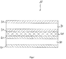
- the figure shows a substrate 10.
- This substrate 10 essentially comprises two layers, namely a first layer 20, which consists of a first metal material (or has a first metal material) and a second layer 30, which consists for example of a plastic material (or has a plastic material).
- the first layer 20 consists in particular of a stainless steel material and has a first coating 21. It is clear that both sides of the first layer 20 are formed with the first coating 21.
- the first coating is in particular a silver coating.
- the second layer 30 also has a coating, namely a second coating 31.
- the second layer 30, which consists of a plastic material, is also formed on both sides with the second coating 31.
- the two layers 20 and 30 are connected to one another by means of a pressure-activatable adhesive 40.
- the pressure-activatable adhesive 40 is placed, for example, in the form of a film between the two layers 20 and 30, in particular between an upper first coating 21 and a lower second coating 31.
- the adhesive material 40 which is located on a carrier film, is activated by means of a lamination process, so that a connection is formed between the first layer 20 and the second layer 30.
- the pressure-activatable adhesive 40 can be an acrylate adhesive or a rubber adhesive and / or a polysiloxane adhesive and / or an acrylic adhesive. The use of a phenol and / or an epoxide and / or a polyurethane is also possible.
- the first coating 21 is preferably formed from such a material so that it serves particularly well for contacting a bonding wire.
- the second coating 31, is designed such that the second coating 31 is or can be contacted by a second contact element, in particular a connection of an antenna.
Landscapes
- Engineering & Computer Science (AREA)
- Computer Hardware Design (AREA)
- Microelectronics & Electronic Packaging (AREA)
- Physics & Mathematics (AREA)
- General Physics & Mathematics (AREA)
- Theoretical Computer Science (AREA)
- Laminated Bodies (AREA)
Priority Applications (1)
| Application Number | Priority Date | Filing Date | Title |
|---|---|---|---|
| EP18213343.9A EP3670175A1 (fr) | 2018-12-18 | 2018-12-18 | Substrat et procédé de fabrication d'un substrat |
Applications Claiming Priority (1)
| Application Number | Priority Date | Filing Date | Title |
|---|---|---|---|
| EP18213343.9A EP3670175A1 (fr) | 2018-12-18 | 2018-12-18 | Substrat et procédé de fabrication d'un substrat |
Publications (1)
| Publication Number | Publication Date |
|---|---|
| EP3670175A1 true EP3670175A1 (fr) | 2020-06-24 |
Family
ID=64744586
Family Applications (1)
| Application Number | Title | Priority Date | Filing Date |
|---|---|---|---|
| EP18213343.9A Withdrawn EP3670175A1 (fr) | 2018-12-18 | 2018-12-18 | Substrat et procédé de fabrication d'un substrat |
Country Status (1)
| Country | Link |
|---|---|
| EP (1) | EP3670175A1 (fr) |
Citations (6)
| Publication number | Priority date | Publication date | Assignee | Title |
|---|---|---|---|---|
| WO2000051075A1 (fr) * | 1999-02-26 | 2000-08-31 | Ibiden Co., Ltd. | Carte a circuit integre et plaque terminale pour carte a circuit integre |
| JP2004013855A (ja) * | 2002-06-11 | 2004-01-15 | Sony Corp | デュアルインターフェースカードおよびその製造方法 |
| US20150283794A1 (en) * | 2014-04-03 | 2015-10-08 | Infineon Technologies Ag | Chip card substrate and method of forming a chip card substrate |
| US20150286921A1 (en) * | 2014-04-03 | 2015-10-08 | Infineon Technologies Ag | Chip card substrate and method of forming a chip card substrate |
| WO2015179639A1 (fr) * | 2014-05-22 | 2015-11-26 | Composecure, Llc | Cartes de transaction et d'identité ayant une certaine texture et une certaine coloration |
| US20170316300A1 (en) * | 2014-11-03 | 2017-11-02 | Composecure Llc | Ceramic-containing and ceramic composite transaction cards |
-
2018
- 2018-12-18 EP EP18213343.9A patent/EP3670175A1/fr not_active Withdrawn
Patent Citations (6)
| Publication number | Priority date | Publication date | Assignee | Title |
|---|---|---|---|---|
| WO2000051075A1 (fr) * | 1999-02-26 | 2000-08-31 | Ibiden Co., Ltd. | Carte a circuit integre et plaque terminale pour carte a circuit integre |
| JP2004013855A (ja) * | 2002-06-11 | 2004-01-15 | Sony Corp | デュアルインターフェースカードおよびその製造方法 |
| US20150283794A1 (en) * | 2014-04-03 | 2015-10-08 | Infineon Technologies Ag | Chip card substrate and method of forming a chip card substrate |
| US20150286921A1 (en) * | 2014-04-03 | 2015-10-08 | Infineon Technologies Ag | Chip card substrate and method of forming a chip card substrate |
| WO2015179639A1 (fr) * | 2014-05-22 | 2015-11-26 | Composecure, Llc | Cartes de transaction et d'identité ayant une certaine texture et une certaine coloration |
| US20170316300A1 (en) * | 2014-11-03 | 2017-11-02 | Composecure Llc | Ceramic-containing and ceramic composite transaction cards |
Non-Patent Citations (1)
| Title |
|---|
| DATABASE WPI Week 200416, Derwent World Patents Index; AN 2004-161024, XP002792234 * |
Similar Documents
| Publication | Publication Date | Title |
|---|---|---|
| DE68929282T2 (de) | Leitersubstrat, Filmträger, Halbleiteranordnung mit dem Filmträger und Montagestruktur mit der Halbleiteranordnung | |
| DE19920593B4 (de) | Chipträger für ein Chipmodul und Verfahren zur Herstellung des Chipmoduls | |
| EP2259311A2 (fr) | Procédé d'encastrement d'au moins un composant dans un élément de plaquettes | |
| AT10735U1 (de) | Verfahren zur herstellung einer leiterplatte sowie verwendung und leiterplatte | |
| DE69805404T2 (de) | Verfahren zum herstellen kontaktloser karten mit antennenverbindung durch gelötete drähte | |
| DE102006022254B4 (de) | Halbleiterbauteil mit in Kunststoffgehäusemasse eingebetteten Halbleiterbauteilkomponenten, Anordnung für eine Mehrzahl von Halbleiterbauteilen und Verfahren zur Herstellung von Halbleiterbauteilen | |
| DE19522338B4 (de) | Chipträgeranordnung mit einer Durchkontaktierung | |
| DE69108919T2 (de) | Filmträger für tab. | |
| DE69003333T2 (de) | Thermokompressionsverbindung für I.C.-Verpackung. | |
| DE19623826A1 (de) | Trägerelement für Halbleiterchips sowie Verfahren zur Herstellung eines Trägerelements | |
| EP2149858A1 (fr) | Procédé de fabrication d'un dispositif de communication sans fil ou d'un pré-laminé pour un tel dispositif | |
| EP3152985B1 (fr) | Procédé de production d'un arrangement de feuilles et arrangment de feuilles correspondant | |
| WO2012130623A2 (fr) | Semi-produit pour la fabrication d'un module de carte à puce, procédé de fabrication du semi-produit ainsi que procédé de fabrication d'une carte à puce | |
| DE102008034616A1 (de) | Prägefolie und deren Verwendung sowie Verfahren zur Herstellung von Strukturelementen aus Kupfer | |
| DE112009002460B4 (de) | Flexible Leiterplatte | |
| EP3670175A1 (fr) | Substrat et procédé de fabrication d'un substrat | |
| DE102015105119B4 (de) | Chipkartensubstrat, verfahren zur herstellung eines chipkartensubstrats und chipkarte | |
| DE102010030966B4 (de) | Elektrisch leitende Verbindung zwischen zwei Kontaktflächen | |
| EP3259709A1 (fr) | Substrat sous forme de bande pour la fabrication de modules de carte à puce | |
| WO2015067792A1 (fr) | Grille de connexion et son utilisation | |
| DE102005015656B4 (de) | Verfahren zum elektrischen Verbinden von RFID-Chipmodulen mit RFID-Antennen und Transpondern | |
| DE102007025958B4 (de) | Baugruppe mit geklebtem Leistungsbaustein und Verfahren zur Herstellung einer solchen Baugruppe | |
| EP1855510B1 (fr) | Système de couches souple | |
| EP1230679B1 (fr) | Procede pour produire un element support destine a un module a circuit integre | |
| DE102023119538A1 (de) | Einsatz für einen datenträger und verfahren zum herstellen eines einsatzes für einen datenträger |
Legal Events
| Date | Code | Title | Description |
|---|---|---|---|
| PUAI | Public reference made under article 153(3) epc to a published international application that has entered the european phase |
Free format text: ORIGINAL CODE: 0009012 |
|
| STAA | Information on the status of an ep patent application or granted ep patent |
Free format text: STATUS: THE APPLICATION HAS BEEN PUBLISHED |
|
| AK | Designated contracting states |
Kind code of ref document: A1 Designated state(s): AL AT BE BG CH CY CZ DE DK EE ES FI FR GB GR HR HU IE IS IT LI LT LU LV MC MK MT NL NO PL PT RO RS SE SI SK SM TR |
|
| AX | Request for extension of the european patent |
Extension state: BA ME |
|
| STAA | Information on the status of an ep patent application or granted ep patent |
Free format text: STATUS: THE APPLICATION IS DEEMED TO BE WITHDRAWN |
|
| 18D | Application deemed to be withdrawn |
Effective date: 20210112 |