EP3671335B1 - Anzeigetafel, verfahren zur herstellung davon und anzeigevorrichtung - Google Patents
Anzeigetafel, verfahren zur herstellung davon und anzeigevorrichtung Download PDFInfo
- Publication number
- EP3671335B1 EP3671335B1 EP18846834.2A EP18846834A EP3671335B1 EP 3671335 B1 EP3671335 B1 EP 3671335B1 EP 18846834 A EP18846834 A EP 18846834A EP 3671335 B1 EP3671335 B1 EP 3671335B1
- Authority
- EP
- European Patent Office
- Prior art keywords
- layer
- region
- display panel
- pad
- elevated
- Prior art date
- Legal status (The legal status is an assumption and is not a legal conclusion. Google has not performed a legal analysis and makes no representation as to the accuracy of the status listed.)
- Active
Links
Images


Classifications
-
- G—PHYSICS
- G02—OPTICS
- G02F—OPTICAL DEVICES OR ARRANGEMENTS FOR THE CONTROL OF LIGHT BY MODIFICATION OF THE OPTICAL PROPERTIES OF THE MEDIA OF THE ELEMENTS INVOLVED THEREIN; NON-LINEAR OPTICS; FREQUENCY-CHANGING OF LIGHT; OPTICAL LOGIC ELEMENTS; OPTICAL ANALOGUE/DIGITAL CONVERTERS
- G02F1/00—Devices or arrangements for the control of the intensity, colour, phase, polarisation or direction of light arriving from an independent light source, e.g. switching, gating or modulating; Non-linear optics
- G02F1/01—Devices or arrangements for the control of the intensity, colour, phase, polarisation or direction of light arriving from an independent light source, e.g. switching, gating or modulating; Non-linear optics for the control of the intensity, phase, polarisation or colour
- G02F1/13—Devices or arrangements for the control of the intensity, colour, phase, polarisation or direction of light arriving from an independent light source, e.g. switching, gating or modulating; Non-linear optics for the control of the intensity, phase, polarisation or colour based on liquid crystals, e.g. single liquid crystal display cells
- G02F1/133—Constructional arrangements; Operation of liquid crystal cells; Circuit arrangements
- G02F1/1333—Constructional arrangements; Manufacturing methods
- G02F1/1339—Gaskets; Spacers; Sealing of cells
- G02F1/13394—Gaskets; Spacers; Sealing of cells spacers regularly patterned on the cell subtrate, e.g. walls, pillars
-
- H—ELECTRICITY
- H10—SEMICONDUCTOR DEVICES; ELECTRIC SOLID-STATE DEVICES NOT OTHERWISE PROVIDED FOR
- H10D—INORGANIC ELECTRIC SEMICONDUCTOR DEVICES
- H10D86/00—Integrated devices formed in or on insulating or conducting substrates, e.g. formed in silicon-on-insulator [SOI] substrates or on stainless steel or glass substrates
- H10D86/01—Manufacture or treatment
- H10D86/021—Manufacture or treatment of multiple TFTs
- H10D86/0231—Manufacture or treatment of multiple TFTs using masks, e.g. half-tone masks
-
- H—ELECTRICITY
- H10—SEMICONDUCTOR DEVICES; ELECTRIC SOLID-STATE DEVICES NOT OTHERWISE PROVIDED FOR
- H10D—INORGANIC ELECTRIC SEMICONDUCTOR DEVICES
- H10D86/00—Integrated devices formed in or on insulating or conducting substrates, e.g. formed in silicon-on-insulator [SOI] substrates or on stainless steel or glass substrates
- H10D86/40—Integrated devices formed in or on insulating or conducting substrates, e.g. formed in silicon-on-insulator [SOI] substrates or on stainless steel or glass substrates characterised by multiple TFTs
- H10D86/441—Interconnections, e.g. scanning lines
-
- H—ELECTRICITY
- H10—SEMICONDUCTOR DEVICES; ELECTRIC SOLID-STATE DEVICES NOT OTHERWISE PROVIDED FOR
- H10D—INORGANIC ELECTRIC SEMICONDUCTOR DEVICES
- H10D86/00—Integrated devices formed in or on insulating or conducting substrates, e.g. formed in silicon-on-insulator [SOI] substrates or on stainless steel or glass substrates
- H10D86/40—Integrated devices formed in or on insulating or conducting substrates, e.g. formed in silicon-on-insulator [SOI] substrates or on stainless steel or glass substrates characterised by multiple TFTs
- H10D86/60—Integrated devices formed in or on insulating or conducting substrates, e.g. formed in silicon-on-insulator [SOI] substrates or on stainless steel or glass substrates characterised by multiple TFTs wherein the TFTs are in active matrices
-
- G—PHYSICS
- G02—OPTICS
- G02F—OPTICAL DEVICES OR ARRANGEMENTS FOR THE CONTROL OF LIGHT BY MODIFICATION OF THE OPTICAL PROPERTIES OF THE MEDIA OF THE ELEMENTS INVOLVED THEREIN; NON-LINEAR OPTICS; FREQUENCY-CHANGING OF LIGHT; OPTICAL LOGIC ELEMENTS; OPTICAL ANALOGUE/DIGITAL CONVERTERS
- G02F1/00—Devices or arrangements for the control of the intensity, colour, phase, polarisation or direction of light arriving from an independent light source, e.g. switching, gating or modulating; Non-linear optics
- G02F1/01—Devices or arrangements for the control of the intensity, colour, phase, polarisation or direction of light arriving from an independent light source, e.g. switching, gating or modulating; Non-linear optics for the control of the intensity, phase, polarisation or colour
- G02F1/13—Devices or arrangements for the control of the intensity, colour, phase, polarisation or direction of light arriving from an independent light source, e.g. switching, gating or modulating; Non-linear optics for the control of the intensity, phase, polarisation or colour based on liquid crystals, e.g. single liquid crystal display cells
- G02F1/133—Constructional arrangements; Operation of liquid crystal cells; Circuit arrangements
- G02F1/136—Liquid crystal cells structurally associated with a semi-conducting layer or substrate, e.g. cells forming part of an integrated circuit
- G02F1/1362—Active matrix addressed cells
- G02F1/136286—Wiring, e.g. gate line, drain line
- G02F1/136295—Materials; Compositions; Manufacture processes
Definitions
- the present disclosure relates to the field of display technology, and particularly to a display panel, a manufacturing method thereof, and a display device.
- An existing display panel usually includes two display substrates cell-assembled with each other, a liquid crystal (LC) layer filled between the two display substrates, and a spacer which is disposed in a non-aperture region of one of the two display substrates and is configured to maintain a cell thickness.
- LC liquid crystal
- CF color filter
- US20060281211A1 relates to a liquid crystal display panel, comprising an upper substrate, a lower substrate facing the upper substrate, a gate line and a data line on an upper surface of the lower substrate facing the upper substrate, the gate line and the data line cross each other to define a cell area, a pixel electrode formed in the cell area, a dummy source/drain electrode pattern over the gate line, and a ball spacer within the dummy source/drain electrode pattern, the ball spacer maintaining a cell gap between the upper substrate and the lower substrate.
- US20080266498A1 relates to an LCD device, comprising: a first substrate, a second substrate, a spacer interposed between the first substrate and the second substrate, and a barrier.
- the preamble of claim 1 is based on the display panel in Figures 13 and 14 of this disclosure.
- US2017019941A1 relates to an array substrate, where a connection part for connecting two adjacent pixel electrodes is configured to enclose the spacer from three sides and a corresponding thin film transistor is arranged to enclose the spacer from a side other than the three sides.
- US20170153480A1 relates to a liquid crystal display panel, wherein one convex part is provided respectively on the array substrate corresponding to two sides of each sub spacer, which is equivalent to forming one recess between two convex parts, and thus to make the sub spacer being wedged in the recess.
- the present disclosure provides a display panel to solve at least one technical problem mentioned above.
- a display panel including an array substrate which includes a plurality of pixel regions defined by a plurality of gate lines intersected with a plurality of data lines, wherein each of the pixel regions includes an aperture region, a non-aperture region surrounding the aperture region, and a spacer disposed in the non-aperture region, and each of the pixel regions further comprising: a padding structure provided in the non-aperture region, the padding structure comprising a first pad and a second pad located in the non-aperture region, the first pad and the second pad being located, in plan view, at two sides of the spacer, respectively, and the first pad and the second pad being located, in plan view, at two sides of the gate line, respectively, and the padding structure is configured to prevent the spacer from moving into the aperture region.
- the display panel includes a first base substrate and a gate line located in a region of the first base substrate corresponding to the non-aperture region; the spacer is located in an area of the non-aperture region corresponding to the gate line and right above the gate line; the padding structure is located on the first base substrate; and a total thickness of a film layer structure in a region on the first base substrate corresponding to the first pad is greater than a total thickness of a film layer structure in a region on the first base substrate corresponding to the gate line; a total thickness of a film layer structure in a region on the first base substrate corresponding to the second pad is greater than the total thickness of the film layer structure in the region on the first base substrate corresponding to the gate line.
- the first pad includes at least one of: a first elevated layer located in a same layer with the gate line, a second elevated layer located in a same layer with a data line, and a third elevated layer located in a same layer with an active layer; the second pad includes at least one of: a fourth elevated layer located in a same layer with the gate line, a fifth elevated layer located in a same layer with the data line, and a sixth elevated layer located in a same layer with the active layer.
- the display panel further includes a common electrode line, the common electrode line is located in a same layer with the gate line and is located at one side of the gate line; the first pad corresponds to the common electrode line, and a portion of the common electrode line corresponding to the first pad serves as the first elevated layer; or, the second pad corresponds to the common electrode line, and a portion of the common electrode line corresponding to the second pad serves as the fourth elevated layer.
- the manufacturing method of the display panel includes: forming a padding structure in a non-aperture region in each of the plurality of pixel regions of the display panel, the padding structure comprising a first pad and a second pad located in the non-aperture region, the first pad and the second pad being located, in plan view, at two sides of the spacer, respectively, and the first pad and the second pad being located, in plan view, at two sides of the gate line, respectively, and the padding structure being configured to prevent the spacer from moving into an aperture region.
- the spacer is located in an area of the non-aperture region corresponding to a gate line and right above the gate line; the padding structure includes a first pad and a second pad.
- the step of forming a padding structure in a non-aperture region of the display panel includes:
- the first pad includes at least one of a first elevated layer, a second elevated layer and a third elevated layer.
- the step of forming the first pad in a region on the first base substrate corresponding to the non-aperture region of the display panel includes at least one of:
- the display panel includes a common electrode line, the common electrode line is located in a same layer with the gate line and is located at one side of the gate line; the first pad corresponds to the common electrode line.
- the step of forming the first elevated layer in a region on the first base substrate corresponding to the non-aperture region of the display panel includes: forming the common electrode line in the region on the first base substrate corresponding to the non-aperture region of the display panel, and a portion of the common electrode line corresponding to the first pad serving as the first elevated layer;
- the first elevated layer is formed along with the gate line by a single patterning process; the second elevated layer is formed along with the date line by a single patterning process; and the third elevated layer is formed along with the active layer by a single patterning process.
- the second elevated layer is formed along with the third elevated layer by a single patterning process.
- the manufacturing method of the display panel includes: forming a padding structure in a non-aperture region in each of the plurality of pixel regions of the display panel, the padding structure comprising a first pad and a second pad located in the non-aperture region, the first pad and the second pad being located, in plan view, at two sides of the spacer, respectively, and the first pad and the second pad being located, in plan view, at two sides of the gate line, respectively, and the padding structure being configured to prevent the spacer from moving into an aperture region.
- the spacer is located in an area of the non-aperture region corresponding to a gate line and right above the gate line; the padding structure includes a first pad and a second pad.
- the step of forming a padding structure in a non-aperture region of the display panel includes:
- the second pad includes at least one of a fourth elevated layer, a fifth elevated layer and a sixth elevated layer.
- the step of forming the second pad in a region on the first base substrate corresponding to the non-aperture region of the display panel includes at least one of:
- the display panel includes a common electrode line, the common electrode line is located in a same layer with the gate line and is located at a side of the gate line; the second pad corresponds to the common electrode line.
- the step of forming the fourth elevated layer in a region on the first base substrate corresponding to the non-aperture region of the display panel includes: forming the common electrode line in the region on the first base substrate corresponding to the non-aperture region of the display panel, and a portion of the common electrode line corresponding to the second pad serving as the fourth elevated layer.
- the fourth elevated layer is formed along with the gate line by a single patterning process; the fifth elevated layer is formed along with the date line by a single patterning process; and the sixth elevated layer is formed along with the active layer by a single patterning process.
- the fifth elevated layer is formed along with the sixth elevated layer by a single patterning process.
- a display device including the display panel described in the technical solutions above.
- FIG. 1 is a plan view of a display panel not according to the present invention.
- an array substrate includes a plurality of pixel regions defined by a plurality of gate lines 11 intersected with a plurality of data lines 13; each of the pixel regions includes an aperture region 1 (i.e., the aperture region of the display panel) and a non-aperture region 2 (i.e., the non-aperture region of the display panel) surrounding the aperture region 1; and a spacer 20 usually is disposed in an area of the non-aperture region 2 corresponding to the gate line.
- the spacer 20 disposed in the non-aperture region 2 of the array substrate although having the ability of supporting a cell body so as to maintain a cell thickness, still involves problems as below: after the array substrate is cell-assembled with a color filter (CF) substrate to form the display panel, if the display panel is applied with a certain external force, the spacer 20 may be moved into the aperture region 1 under the action of the external force, which would not only affect an arrangement of liquid crystals (LCs) around the spacer 20 but also block light transmitted through the aperture region 1, thereby resulting in a decrease of an aperture ratio and influencing a display performance of the display panel.
- CF color filter
- a display panel provided by an embodiment of the present disclosure includes an aperture region 1, a non-aperture region 2 surrounding the aperture region 1, and a spacer 20 disposed in the non-aperture region 2; the non-aperture region 2 is further provided with a padding structure 30, the padding structure 30 is located near the spacer 20 and is configured to prevent the spacer 20 from moving into the aperture region 1.
- the display panel provided by the embodiment of the present disclosure includes an array substrate and a CF substrate which are cell-assembled with each other.
- the array substrate incudes a first base substrate 10 and a plurality of pixel regions located on the first base substrate 10, the plurality of pixels are defined by a plurality of gate lines 11 intersected with a plurality of data lines 13.
- Each of the pixel regions includes an aperture region 1 (i.e., the aperture region 1 of the display panel) and a non-aperture region 2 (i.e., the non-aperture region of the display panel) surrounding the aperture region 1; and each of the pixel regions is provided with a corresponding pixel unit; each pixel unit includes a thin film transistor (TFT) 14 and a pixel electrode 16; the TFT 14 may be a bottom-gate TFT, and the TFT 14 includes a gate electrode 141, a gate insulating layer 142, an active layer 143, a source electrode 144 and a drain electrode 145.
- TFT thin film transistor
- the gate electrode 141 of the TFT 14 is located on a first base substrate 10, and the gate electrode 141 is connected to a corresponding gate line 11.
- the gate electrode 141 and the gate line 11 are formed by a single patterning process.
- a material of the gate electrode 141 and the gate line 11 may be selected as a single metal material such as copper (Cu), aluminum (Al), molybdenum (Mo), titanium (Ti), chromium (Cr) and tungsten (W), and may also be selected as an alloy material consisted of at least two of the single metal materials described above.
- a structure of the gate line 11 and the gate electrode 141 in a direction perpendicular to the first base substrate 10 may be a single-layered structure, and may also be a multi-layered structure.
- the gate line 11 and the gate electrode 141 may include a sandwiched structure consisted of two Mo structural layers and one Al structural layer (i.e., a Mo ⁇ Al ⁇ Mo structure), or it may include a sandwiched structure consisted of two Ti structural layers and one Cu structural layer (i.e., a Ti ⁇ Cu ⁇ Ti structure), or, it may include a double-layered structure consisted of a Mo-Ti alloy structural layer and a Cu structural layer (i.e., a MoTi ⁇ Cu structure).
- the gate insulating layer 142 covers the first base substrate 10 and the gate electrode 141; a material of the gate insulating layer 142 may adopt silicon nitride or silicon oxide; and the gate insulating layer 142 may be a single-layered structure and may also be a multi-layered structure.
- the gate insulating layer 142 may include a double-layered structure consisted of a silicon oxide structural layer and a silicon nitride structural layer (i.e., a silicon oxide ⁇ silicon nitride structure).
- the active layer 143 is located on the gate insulating layer 142 and is corresponding to the gate electrode 141; a material of the active layer 143 may be amorphous silicon, monocrystalline silicon, polycrystalline silicon or metal oxide semiconductor material.
- a material of the active layer 143 may be amorphous silicon, monocrystalline silicon, polycrystalline silicon or metal oxide semiconductor material.
- the material of the active layer 143 is selected as a metal oxide semiconductor material, in may be Indium Gallium Zinc Oxide (IGZO), zinc oxide (ZnO) or the like.
- the source electrode 144 and the drain electrode 145 are in contact with the active layer 143, respectively; the source electrode 144, the drain electrode 145 and the data line 13 are disposed in a same layer and are formed by a single patterning process; the source electrode 144 is connected to a corresponding data line 13, and the drain electrode 145 is connected to a corresponding pixel electrode 16.
- a material of the source electrode 144, the drain electrode 145 and the data line 13 may be selected as a single metal material such as copper (Cu), aluminum (Al), molybdenum (Mo), titanium (Ti), chromium (Cr) and tungsten (W), and may also be selected as an alloy material consisted of at least two of the single metal materials described above.
- a structure of the source electrode 144, the drain electrode 145 and the data line 13 in the direction perpendicular to the first base substrate 10 may be a single-layered structure, and may also be a multi-layered structure.
- the source electrode 144, the drain electrode 145 and the data line 13 are in a multi-layered structure, it may include a sandwiched structure consisted of two Mo structural layers and one Al structural layer (i.e., a Mo ⁇ Al ⁇ Mo structure), or it may include a sandwiched structure consisted of two Ti structural layers and one Cu structural layer (i.e., a Ti ⁇ Cu ⁇ Ti structure), or, it may include a double-layered structure consisted of a Mo-Ti alloy structural layer and a Cu structural layer (i.e., a MoTi ⁇ Cu structure).
- the pixel electrode 16 is located above the TFT 14, and is located in a corresponding aperture region 1.
- a passivation layer 15 is formed between the pixel electrode 16 and the TFT 14, and the passivation layer 15 covers the gate insulating layer 142, the source electrode 144, the drain electrode 145, the data line 13 and the active layer 143.
- a material of the passivation layer 15 may adopt silicon nitride or silicon oxide; and the passivation layer 15 may be a single-layered structure and may also be a multi-layered structure.
- the passivation layer 15 When the passivation layer 15 is a multi-layered structure, it can include a double-layered structure consisted of a silicon oxide structural layer and a silicon nitride structural layer (i.e., a silicon oxide ⁇ silicon nitride structure).
- a portion of the passivation layer 15 corresponding to the drain electrode 145 is provided with a via hole, and the pixel electrode 16 is connected to a corresponding drain electrode 145 through a corresponding via hole.
- a material of the pixel electrode 16 may be selected as Indium Tin Oxide (ITO), Indium Zinc Oxide (IZO) or other transparent metal oxide conductive materials.
- the CF substrate includes a second base substrate 40, as well as a black matrix 42 and a CF layer 41 which are formed on the second base substrate 40;
- the black matrix 42 defines a plurality of aperture regions 1(i.e., the aperture region 1 of the display panel; the non-aperture region 2 of the display panel corresponds to the black matrix 42);
- the black matrix 42 corresponds to the gate line 11, the data line 13 and the TFT 14;
- the CF layer 41 is located in a region on the second base substrate 40 corresponding to the aperture region 1.
- a spacer 20 is formed between the array substrate and the CF substrate.
- the spacer 20 is configured to support the cell body so as to maintain a certain cell thickness.
- the spacer 20 may be disposed in a region on the array substrate corresponding to the non-aperture region 2 (it may also be interpreted as a region corresponding to the black matrix 42), and located in an area of the non-aperture region 2 corresponding to the gate line 11 on the array substrate; or, the spacer 20 may also be disposed in a region on the CF substrate corresponding to the non-aperture region 2, and located in an area of the non-aperture region 2 corresponding to the gate line 11 on the array substrate; it may also be interpreted that, the spacer 20 is disposed in a region of the black matrix 42 on the CF substrate corresponding to the gate line 11.
- the non-aperture region 2 is further provided with a padding structure 30, the padding structure 30 may be disposed in a region on the array substrate corresponding to the non-aperture region 2, and may also be disposed in a region on the CF substrate corresponding to the non-aperture region 2.
- the padding structure 30 is located near the spacer 20, and is configured to limit a position of the spacer 20 so as to prevent the spacer 20 from moving into the aperture region 1 of the display panel.
- the position of the spacer 20 can be limited, so as to prevent the spacer 20 from moving into the aperture region 1 of the display panel.
- the padding structure 30 is disposed in the non-aperture region 2 and is located near the spacer 20.
- the padding structure 30 may be disposed at one side of the spacer 20; or, the padding structure 30 may be disposed at two opposite sides of the spacer 20; or, the padding structure 30 may be disposed to surround the spacer 20.
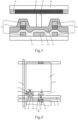
- the display panel provided by the present disclosure includes a first base substrate 10, and a gate line 11 located in a region on the first base substrate 10 corresponding to the non-aperture region 2; the spacer 20 is located in an area of the non-aperture region 2 corresponding to the gate line 11.
- the padding structure is located on the first base substrate 10; the padding structure 30 includes a first pad 31 and a second pad 32 located in the non-aperture region 2; the first pad 31 and the second pad 32 are located at two sides of the spacer 20, respectively; and the first pad 31 and the second pad 32 are located at two sides of the gate line 11, respectively.
- a total thickness of a film layer structure in a region on the first base substrate 10 corresponding to the first pad 31 is greater than a total thickness of a film layer structure in a region on the first base substrate 10 corresponding to the gate line 11.
- a total thickness of a film layer structure in a region on the first base substrate 10 corresponding to the second pad 32 is greater than the total thickness of the film layer structure in the region on the first base substrate 10 corresponding to the gate line 11.
- the spacer 20 is located in an area of the non-aperture region 2 corresponding to the gate line 11 and right above the gate line 11 as illustrated in FIG. 3 or FIG. 5 .
- the padding structure 30 includes a first pad 31 and a second pad 32.
- the first pad 31 and the second pad 32 are located at two sides of the spacer 20, respectively; and the first pad 31 and the second pad 32 are located at two sides of the gate line 11, respectively.
- the first pad 31 is located between an upper aperture region 1 illustrated in FIG. 2 or FIG. 4 and the spacer 20; and the second pad 32 is located between a lower aperture region 1 illustrated in FIG. 2 or FIG. 4 and the spacer 20.
- a total thickness of a film layer structure in a region on the first base substrate 10 corresponding to the first pad 31 is greater than a total thickness of a film layer structure in a region on the first base substrate 10 corresponding to the gate line 11; a total thickness of a film layer structure in a region on the first base substrate 10 corresponding to the second pad 32 is greater than the total thickness of the film layer structure in the region on the first base substrate 10 corresponding to the gate line 11.
- film layers in a region on the first base substrate 10 corresponding to the first pad 31 include a first pad 31, a gate insulating layer 142 and a passivation layer 15; film layers in a region on the first base substrate 10 corresponding to the second pad 32 include a second pad 32, a gate insulating layer 142 and a passivation layer 15; film layers in a region on the first base substrate 10 corresponding to the gate line 11 include a gate line 11, a gate insulating layer 142 and a passivation layer 15.
- a total thickness of the first pad 31, the gate insulating layer 142 and the passivation layer 15 is greater than a total thickness of the gate line 11, the gate insulating layer 142 and the passivation layer 15; a total thickness of the second pad 32, the gate insulating layer 142 and the passivation layer 15 is greater than the total thickness of the gate line 11, the gate insulating layer 142 and the passivation layer 15. That is to say, as illustrated in FIG. 3 or FIG. 5 , a region on a top of the first base substrate 10 corresponding to the spacer 20 is formed into a groove, and the spacer 20 is located in the groove; a groove wall of the groove blocks both sides of the spacer 20 so as to prevent the spacer 20 from moving into the aperture region 1.
- the first pad 31 and the second pad 32 are disposed at opposite two sides of the spacer 20 respectively, and are located at two sides of the gate line 11 respectively; as a result, the first pad 31 and the second pad 32 are respectively located between a corresponding aperture region 1 and the spacer 20 to block the spacer 20 and limit the position of the spacer 20, so as to prevent the spacer 20 from moving into the aperture region 1.
- the first pad 31 may be arranged in various forms.
- the first pad 31 may include: a first elevated layer 311 located in a same layer with the gate line 11, and/or, a second elevated layer 312 located in a same layer with the data line 13, and/or, a third elevated layer 313 located in a same layer with the active layer 143. That is to say, the first pad 31 may include at least one of the first elevated layer 311, the second elevated layer 312 and the third elevated layer 313. Description will be given with reference to FIG.
- film layers in a region on the first base substrate 10 corresponding to the gate line 11 include a gate line 11, a gate insulating layer 142 and a passivation layer 15; film layers in a region on the first base substrate 10 corresponding to the first pad 31 include a first pad 31, a gate insulating layer 142 and a passivation layer 15.
- a thickness of the first pad 31 is greater than a thickness of the gate line 11, so that a total thickness of a film layer structure in a region on the first base substrate 10 corresponding to the first pad 31 is greater than a total thickness of a film layer structure in a region on the first base substrate 10 corresponding to the gate line 11.
- a thickness of the first elevated layer 311 is greater than a thickness of the gate line 11; when the first pad 31 includes only the second elevated layer 312, a thickness of the second elevated layer 312 is greater than a thickness of the data line 13; and when the first pad 31 includes only the third elevated layer 313, a thickness of the third elevated layer 313 is greater than a thickness of the active layer 143.
- the first elevated layer 311 is located in a same layer with the gate line 11; the first elevated layer 311 may be formed separately, and may also be formed along with the gate line 11 by a single patterning process; the first elevated layer 311 may be formed along with the gate line 11 by a single patterning process.
- the second elevated layer 312 is located in a same layer with the data line 13; the second elevated layer 312 may be formed separately, and may also be formed along with the data line 13 by a single patterning process; the second elevated layer 312 may be formed along with the data line 13 by a single patterning process.
- the third elevated layer 313 is located in a same layer with the active layer 143; the third elevated layer 313 may be formed separately, and may also be formed along with the active layer 143 by a single patterning process; the third elevated layer 313 may be formed along with the active layer 143 by a single patterning process.
- the second pad 32 may be arranged in various forms.
- the second pad 32 may include: a fourth elevated layer 321 located in a same layer with the gate line 11, and/or, a fifth elevated layer 322 located in a same layer with the data line 13, and/or, a sixth elevated layer 323 located in a same layer with the active layer 143. That is to say, the second pad 32 may include at least one of the fourth elevated layer 321, the fifth elevated layer 322 and the sixth elevated layer 323. Description will be given with reference to FIG.
- film layers in a region on the first base substrate 10 corresponding to the gate line 11 include a gate line 11, a gate insulating layer 142 and a passivation layer 15; film layers in a region on the first base substrate 10 corresponding to the second pad 32 include a second pad 32, a gate insulating layer 142 and a passivation layer 15.
- a thickness of the second pad 32 is greater than a thickness of the gate line 11, so that a total thickness of a film layer structure in a region on the first base substrate 10 corresponding to the second pad 32 is greater than a total thickness of a film layer structure in a region on the first base substrate 10 corresponding to the gate line 11.
- a thickness of the second elevated layer 321 is greater than a thickness of the gate line 11; when the second pad 32 includes only the fifth elevated layer 322, a thickness of the fifth elevated layer 322 is greater than a thickness of the data line 13; and when the second pad 32 includes only the sixth elevated layer 323, a thickness of the sixth elevated layer 323 is greater than a thickness of the active layer 143.
- the fourth elevated layer 321 is located in a same layer with the gate line 11; the fourth elevated layer 321 may be formed separately, and may also be formed along with the gate line 11 by a single patterning process; the fourth elevated layer 321 may be formed along with the gate line 11 by a single patterning process.
- the fifth elevated layer 322 is located in a same layer with the data line 13; the fifth elevated layer 322 may be formed separately, and may also be formed along with the data line 13 by a single patterning process; the fifth elevated layer 322 may be formed along with the data line 13 by a single patterning process.
- the sixth elevated layer 323 is located in a same layer with the active layer 143; the sixth elevated layer 323 may be formed separately, and may also be formed along with the active layer 143 by a single patterning process; the sixth elevated layer 323 may be formed along with the active layer 143 by a single patterning process.
- the display panel further includes a common electrode line 12, the common electrode line 12 is located in a same layer with the gate line 11, and the common electrode line 12 is located at one side of the gate line 11; in such case, the first pad 31 may be arranged to correspond to the common electrode line 12, and a portion of the common electrode line 12 corresponding to the first pad 31 may serve as the first elevated layer 311 of the first pad 31; or, referring to FIG. 4 and FIG. 5 , the second pad 32 may also be arranged to correspond to the common electrode line 12, and a portion of the common electrode line 12 corresponding to the second pad 32 may serve as the fourth elevated layer 321 of the second pad 32.
- the portion of the common electrode line 12 corresponding to the first pad 31 serves as the first elevated layer 311 of the first pad, or, the portion of the common electrode line 12 corresponding to the second pad 32 serves as the fourth elevated layer 321 of the second pad 32, and the common electrode line 12 is formed in a same layer with the gate line 11 so that the common electrode line 12 can be formed along with the gate line 11 by a single patterning process; in this way, the process steps in manufacturing the display panel can be reduced and the number of mask necessary for manufacturing the display panel can be decreased, so as to lower the cost of manufacturing the display panel and improve the efficiency of manufacturing the display panel.
- the portion of the common electrode line 12 corresponding to the first pad 31 serves as the first elevated layer 311 of the first pad, or, the portion of the common electrode line 12 corresponding to the second pad 32 serves as the fourth elevated layer 321 of the second pad 32; in this way, it has no need of providing a small region on the mask as used so as to form the first elevated layer 311 or the fourth elevated layer 321, which can simplify the structure of the mask, and hence can lower the cost of manufacturing the display panel.
- the embodiment of the present disclosure further provides a display device, and the display device includes the display panel described in the embodiments above.
- the display device possesses the same advantages with that of the display panel described above, without repeating herein.
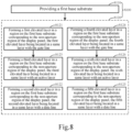
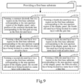
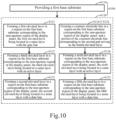
- the present disclosure further provides a manufacturing method of a display panel, for manufacturing the display panel described in the embodiments above.
- the manufacturing method of the display panel includes steps as below.
- a padding structure is formed in a non-aperture region of the display panel.
- the padding structure is located near a spacer disposed in the non-aperture region and is configured to prevent the spacer from moving into an aperture region.
- the step S100 of forming a padding structure in a non-aperture region of the display panel includes the following steps.
- step S 110 a first base substrate is provided.
- a first pad and a second pad are formed in a region on the first base substrate corresponding to the non-aperture region of the display panel, in which the first pad and the second pad are located at two sides of the spacer, respectively, and the first pad and the second pad are located at two sides of the gate line, respectively.
- a total thickness of a film layer structure in a region on the first base substrate corresponding to the first pad is greater than a total thickness of a film layer structure in a region on the first base substrate corresponding to the gate line; and a total thickness of a film layer structure in a region on the first base substrate corresponding to the second pad is greater than the total thickness of the film layer structure in the region on the first base substrate corresponding to the gate line.
- the first pad may include at least one of: a first elevated layer located in a same layer with the gate line, a second elevated layer located in a same layer with a data line, and a third elevated layer located in a same layer with an active layer.
- the step S120 of forming the first pad in a region on the first base substrate corresponding to the non-aperture region of the display panel may include the following step.
- a first elevated layer is formed in a region on the first base substrate corresponding to the non-aperture region of the display panel, and the first elevated layer is located in a same layer with the gate line.
- the step S120 of forming a first pad in a region on the first base substrate corresponding to the non-aperture region of the display panel may include the following step S122.
- a second elevated layer is formed in a region on the first base substrate corresponding to the non-aperture region of the display panel, the second elevated layer being located in a same layer with a data line.
- the step S120 of forming a first pad in a region on the first base substrate corresponding to the non-aperture region of the display panel may include step S123.
- a third elevated layer is formed in a region on the first base substrate corresponding to the non-aperture region of the display panel, the third elevated layer being located in a same layer with an active layer.
- the step S120 of forming a first pad in a region on the first base substrate corresponding to the non-aperture region of the display panel may include the following steps.
- a first elevated layer is formed in a region on the first base substrate corresponding to the non-aperture region of the display panel, the first elevated layer being located in a same layer with the gate line.
- a second elevated layer is formed in a region on the first base substrate corresponding to the non-aperture region of the display panel, the second elevated layer being located in a same layer with a data line.
- the step S120 of forming a first pad in a region on the first base substrate corresponding to the non-aperture region of the display panel may include the following steps.
- a first elevated layer is formed in a region on the first base substrate corresponding to the non-aperture region of the display panel, the first elevated layer being located in a same layer with the gate line.
- a third elevated layer is formed in a region on the first base substrate corresponding to the non-aperture region of the display panel, the third elevated layer being located in a same layer with an active layer.
- the step S120 of forming a first pad in a region on the first base substrate corresponding to the non-aperture region of the display panel may include the following steps.
- a third elevated layer is formed in a region on the first base substrate corresponding to the non-aperture region of the display panel, the third elevated layer being located in a same layer with an active layer.
- a second elevated layer is formed in a region on the first base substrate corresponding to the non-aperture region of the display panel, the second elevated layer being located in a same layer with a data line.
- the step S120 of forming a first pad in a region on the first base substrate corresponding to the non-aperture region of the display panel may include the following steps.
- a first elevated layer is formed in a region on the first base substrate corresponding to the non-aperture region of the display panel, the first elevated layer being located in a same layer with the gate line.
- a third elevated layer is formed in a region on the first base substrate corresponding to the non-aperture region of the display panel, the third elevated layer being located in a same layer with an active layer.
- a second elevated layer is formed in a region on the first base substrate corresponding to the non-aperture region of the display panel, the second elevated layer being located in a same layer with a data line.
- the first elevated layer may be formed along with the gate line by a single patterning process.
- the second elevated layer may be formed along with the date line by a single patterning process.
- the third elevated layer may be formed along with the active layer by a single patterning process.
- the first pad includes both of a second elevated layer and a third elevated layer, i.e., the first pad includes a second elevated layer and a third elevated layer or the first pad includes a first elevated layer, a second elevated layer and a third elevated layer
- the second elevated layer and the third elevated layer may be formed by a single patterning process.
- the second elevated layer is located in a same layer with the data line
- the third elevated layer is located in a same layer with the active layer; correspondingly, when forming the second elevated layer and the third elevated layer, an active layer material layer is formed firstly and a data line material layer is formed subsequently, and then the active layer, the data line, the second elevated layer and the third elevated layer are formed simultaneously by using a mask such as halftone mask; in this way, the process steps in manufacturing the display panel can be reduced, and the number of mask necessary for manufacturing the display panel can be decreased, so as to lower the cost of manufacturing the display panel and improve the efficiency of manufacturing the display panel.
- a mask such as halftone mask
- the second pad may include at least one of a fourth elevated layer, a fifth elevated layer, and a sixth elevated layer.
- the step S120 of forming a second pad in a region on the first base substrate corresponding to the non-aperture region of the display panel may include the following step.
- a fourth elevated layer is formed in a region on the first base substrate corresponding to the non-aperture region of the display panel, the fourth elevated layer being located in a same layer with the gate line.
- the step S120 of forming a second pad in a region on the first base substrate corresponding to the non-aperture region of the display panel may include the following step.
- a fifth elevated layer is formed in a region on the first base substrate corresponding to the non-aperture region of the display panel, the fifth elevated layer being located in a same layer with a data line.
- the step S120 of forming a second pad in a region on the first base substrate corresponding to the non-aperture region of the display panel may include the following step.
- a sixth elevated layer is formed in a region on the first base substrate corresponding to the non-aperture region of the display panel, the sixth elevated layer being located in a same layer with an active layer.
- the step S120 of forming a second pad in a region on the first base substrate corresponding to the non-aperture region of the display panel may include the following steps.
- a fourth elevated layer is formed in a region on the first base substrate corresponding to the non-aperture region of the display panel, the fourth elevated layer being located in a same layer with the gate line.
- a fifth elevated layer is formed in a region on the first base substrate corresponding to the non-aperture region of the display panel, the fifth elevated layer being located in a same layer with a data line.
- the step S120 of forming a second pad in a region on the first base substrate corresponding to the non-aperture region of the display panel may include the following steps.
- a fourth elevated layer is formed in a region on the first base substrate corresponding to the non-aperture region of the display panel, the fourth elevated layer being located in a same layer with the gate line.
- a sixth elevated layer is formed in a region on the first base substrate corresponding to the non-aperture region of the display panel, the sixth elevated layer being located in a same layer with an active layer.
- the step S120 of forming a second pad in a region on the first base substrate corresponding to the non-aperture region of the display panel may include the following steps.
- a sixth elevated layer is formed in a region on the first base substrate corresponding to the non-aperture region of the display panel, the sixth elevated layer being located in a same layer with an active layer;
- a fifth elevated layer is formed in a region on the first base substrate corresponding to the non-aperture region of the display panel, the fifth elevated layer being located in a same layer with a data line.
- the step S120 of forming a second pad in a region on the first base substrate corresponding to the non-aperture region of the display panel may include the following steps.
- a fourth elevated layer is formed in a region on the first base substrate corresponding to the non-aperture region of the display panel, the fourth elevated layer being located in a same layer with the gate line.
- a sixth elevated layer is formed in a region on the first base substrate corresponding to the non-aperture region of the display panel, the sixth elevated layer being located in a same layer with an active layer.
- a fifth elevated layer is formed in a region on the first base substrate corresponding to the non-aperture region of the display panel, the fifth elevated layer being located in a same layer with a data line.
- the fourth elevated layer may be formed along with the gate line by a single patterning process.
- the fifth elevated layer may be formed along with the date line by a single patterning process.
- the sixth elevated layer may be formed along with the active layer by a single patterning process.
- the second pad includes both of a fifth elevated layer and a sixth elevated layer, i.e., the second pad includes a fifth elevated layer and a sixth elevated layer or the second pad includes a fourth elevated layer, a fifth elevated layer and a sixth elevated layer
- the fifth elevated layer and the sixth elevated layer may be formed by a single patterning process.
- the fifth elevated layer is located in a same layer with the data line
- the sixth elevated layer is located in a same layer with the active layer; correspondingly, when forming the fifth elevated layer and the sixth elevated layer, an active layer material layer is formed firstly and a data line material layer is formed subsequently, and then the active layer, the data line, the fifth elevated layer and the sixth elevated layer are formed simultaneously by using a mask such as halftone mask; in this way, the process steps in manufacturing the display panel can be reduced, and the number of mask necessary for manufacturing the display panel can be decreased, so as to lower the cost of manufacturing the display panel and improve the efficiency of manufacturing the display panel.
- a mask such as halftone mask
- the display panel further includes a common electrode line, the common electrode line is located in a same layer with the gate line and is located at one side of the gate line, and the first pad may correspond to the common electrode line.
- the step S121 of forming a first elevated layer in a region on the first base substrate corresponding to the non-aperture region of the display panel includes the following step.
- a common electrode line is formed in a region on the first base substrate corresponding to the non-aperture region of the display panel, and a portion of the common electrode line corresponding to the first pad serving as the first elevated layer.
- the common electrode line is located in a same layer with the gate line and is located at one side of the gate line, and the second pad may correspond to the common electrode line.
- the step S124 of forming a fourth elevated layer in a region on the first base substrate corresponding to the non-aperture region of the display panel includes the following step.
- a common electrode line is formed in a region on the first base substrate corresponding to the non-aperture region of the display panel, and a portion of the common electrode line corresponding to the second pad serving as the fourth elevated layer.
- the manufacturing method of the display panel may include: providing a first base substrate.
- a metal layer e.g., an aluminum (Al) layer
- Al aluminum
- a photoresist is coated on the metal layer, then the photoresist is exposed by using a mask, then the photoresist upon exposure is developed to expose a to-be-etched portion in the metal layer, then the to-be-etched portion in the metal layer is removed by using an etching process (dry etching or wet etching), and then the remaining photoresist is removed to achieve the formation of the gate electrode, the gate line, the common electrode line and the first elevated layer.
- the first elevated layer and the common electrode line are disposed at two sides of the gate line, respectively; the second pad corresponds to the common electrode line; and a portion of the common electrode line corresponding to the second pad serves as the fourth elevated layer.
- a gate insulating layer is formed by using a Plasma Enhanced Chemical Vapor Deposition (PECVD) method, the gate insulating layer covers the first base substrate, the gate electrode, the gate line, the common electrode line and the first elevated layer, and a material of the gate insulating layer may be silicon nitride or silicon oxide.
- PECVD Plasma Enhanced Chemical Vapor Deposition
- An active layer material layer is deposited on the gate insulating layer; and an active layer, a third elevated layer and a sixth elevated layer are formed by a single patterning process, in which the sixth elevated layer corresponds to a portion of the common electrode line corresponding to the second pad.
- an amorphous silicon layer may be deposited on the gate insulating layer by using PECVD method, and the active layer, the third elevated layer and the sixth elevated layer are formed by coating a photoresist, exposing the photoresist, developing the photoresist, etching the photoresist and removing the remaining photoresist; or, when the material of the active layer is a metal oxide semiconductor material such as IGZO, a metal oxide semiconductor material layer may be deposited on the gate insulating layer by using a sputtering method, and then the active layer, the third elevated layer and the sixth elevated layer are formed by coating a photoresist, exposing the photoresist, developing the photoresist, etching the photoresist and removing the remaining photoresist.
- a metal layer e.g., Al layer
- a source electrode, a drain electrode, a data line, a second elevated layer and a fifth elevated layer are formed by a single patterning process, in which the source electrode and the drain electrode are in contact with the active layer, respectively, the source electrode is connected to a corresponding data line, the second elevated layer is located on the third elevated layer, and the fifth elevated layer is located on the sixth elevated layer.
- the source electrode, the drain electrode, the data line, the second elevated layer and the fifth elevated layer are formed by coating a photoresist, exposing the photoresist, developing the photoresist, etching the photoresist and removing the remaining photoresist.
- a passivation layer is formed by using a PECVD method; the passivation layer covers the gate insulating layer, the active layer, the source electrode, the drain electrode, the data line, the second elevated layer and the fifth elevated layer; and a via hole is formed at a position in the passivation layer corresponding to the drain electrode by coating a photoresist, exposing the photoresist, developing the photoresist, etching the photoresist and removing the remaining photoresist.
- a material of the passivation layer may be silicon nitride or silicon oxide.
- a transparent metal oxide conductive material layer e.g., an indium tin oxide (ITO) material layer is deposited on the passivation layer by using a sputtering method; a pixel electrode is formed by coating a photoresist, exposing the photoresist, developing the photoresist, etching the photoresist and removing the remaining photoresist; and the pixel electrode is connected to the drain electrode through the via hole in the passivation layer.
- ITO indium tin oxide
Landscapes
- Physics & Mathematics (AREA)
- Nonlinear Science (AREA)
- Mathematical Physics (AREA)
- Chemical & Material Sciences (AREA)
- Crystallography & Structural Chemistry (AREA)
- General Physics & Mathematics (AREA)
- Optics & Photonics (AREA)
- Engineering & Computer Science (AREA)
- Microelectronics & Electronic Packaging (AREA)
- Devices For Indicating Variable Information By Combining Individual Elements (AREA)
- Liquid Crystal (AREA)
Claims (8)
- Anzeigetafel mit einem Array-Substrat, das eine Vielzahl von Pixelbereichen umfasst, die durch eine Vielzahl von Gate-Leitungen (11) definiert sind, die sich mit einer Vielzahl von Datenleitungen (13) schneiden, wobei jede der Pixelbereichen einen Öffnungsbereich (1), einen Nicht-Öffnungsbereich (2), der den Öffnungsbereich (1) umgibt, und einen Abstandshalter (20), der in dem Nicht-Öffnungsbereich (2) angeordnet ist, beinhaltet, und wobei jeder der Pixelbereiche ferner Folgendes umfasst:eine Polsterstruktur (30), die in dem Nicht-Öffnungsbereich (2) vorgesehen ist, wobei die Polsterstruktur (30) ein erstes Dämpfungsglied (31) und ein zweites Dämpfungsglied (32) umfasst, die sich in dem Nicht-Öffnungsbereich (2) befinden, wobei das erste Dämpfungsglied (31) und das zweite Dämpfungsglied (32) in der Draufsicht jeweils an zwei Seiten des Abstandshalters (20) angeordnet sind und das erste Dämpfungsglied (31) und das zweite Dämpfungsglied (32) in Draufsicht jeweils an zwei Seiten der Gate-Leitung (11) angeordnet sind und die Polsterstruktur (30) konfiguriert ist, um zu verhindern, dass sich der Abstandshalter (20) in den Öffnungsbereich (1) bewegt, wobeidie Anzeigetafel ein erstes Basissubstrat (10) und eine Gate-Leitung (11) umfasst, die in einem Bereich auf dem ersten Basissubstrat (10) angeordnet ist, der dem Nicht-Öffnungsbereich (2) entspricht;der Abstandshalter (20) in einem Bereich des Nicht-Öffnungsbereichs (2) entsprechend der Gate-Leitung (11) und direkt über der Gate-Leitung (11) angeordnet ist;sich die Polsterstruktur (30) auf dem ersten Basissubstrat (10) befindet;eine Gesamtdicke einer Filmschichtstruktur in einem Bereich auf dem ersten Basissubstrat (10), der dem ersten Dämpfungsglied (31) entspricht, größer ist als eine Gesamtdicke einer Filmschichtstruktur in einem Bereich auf dem ersten Basissubstrat (10), der der Gate-Leitung (11) entspricht, und eine Gesamtdicke einer Filmschichtstruktur in einem Bereich auf dem ersten Basissubstrat (10), der dem zweiten Dämpfungsglied (32) entspricht, größer ist als die Gesamtdicke der Filmschichtstruktur in dem Bereich auf dem ersten Basissubstrat (10), der der Gate-Leitung (11) entspricht;das erste Dämpfungsglied (31) mindestens eines von Folgendem umfasst: eine erste erhöhte Schicht (311), die sich in derselben Schicht wie die Gate-Leitung (11) befindet, eine zweite erhöhte Schicht (312), die sich in derselben Schicht wie eine Datenleitung (13) befindet, und eine dritte erhöhte Schicht, die sich in derselben Schicht mit einer aktiven Schicht (143) befindet;das zweite Dämpfungsglied (32) mindestens eines von Folgendem umfasst: eine vierte erhöhte Schicht (321), die sich in derselben Schicht wie die Gate-Leitung (11) befindet, eine fünfte erhöhte Schicht (322), die sich in derselben Schicht wie die Datenleitung (13) befindet, und eine sechste erhöhte Schicht (323), die sich in derselben Schicht wie die aktive Schicht (143) befindet; dadurch gekennzeichnetdie Anzeigetafel ferner Folgendes umfasst: eine gemeinsame Elektrodenleitung (12), wobei die gemeinsame Elektrodenleitung (12) in einer gleichen Schicht wie die Gate-Leitung (11) angeordnet ist und auf einer Seite der Gate-Leitung (11) angeordnet ist,wobeidas erste Dämpfungsglied (31) der gemeinsamen Elektrodenleitung (12) entspricht und ein Teil der gemeinsamen Elektrodenleitung (12), der dem ersten Dämpfungsglied (31) entspricht, als die erste erhöhte Schicht (311) dient; oderdas zweite Dämpfungsglied (32) der gemeinsamen Elektrodenleitung (12) entspricht, und ein Abschnitt der gemeinsamen Elektrodenleitung (12), der dem zweiten Dämpfungsglied (32) entspricht, als die vierte erhöhte Schicht (321) dient.
- Anzeigetafel-Herstellungsverfahren zum Herstellen der Anzeigetafel nach Anspruch 1, umfassend:Bilden der Polsterstruktur (30) in dem Nicht-Öffnungsbereich (2) in jedem der Vielzahl von Pixelbereichen der Anzeigetafel, wobeider Schritt des Bildens der Polsterstruktur (30) in dem Nicht-Öffnungsbereich (2) der Anzeigetafel Folgendes umfasst: Bereitstellen des ersten Basissubstrats (10);und Bilden des ersten Dämpfungsglieds (31) und des zweiten Dämpfungsglieds (32) in einem Bereich auf dem ersten Basissubstrat (10), der dem Nicht-Öffnungsbereich (2) der Anzeigetafel entspricht,wobeider Schritt des Bildens des ersten Dämpfungsglieds (31) in einem Bereich auf dem ersten Basissubstrat (10), der dem Nicht-Öffnungsbereich (2) der Anzeigetafel entspricht, mindestens eines der Folgenden umfasst:Bilden der ersten erhöhten Schicht (311) in einem Bereich auf dem ersten Basissubstrat (10), der dem Nicht-Öffnungsbereich (2) der Anzeigetafel entspricht;Bilden der zweiten erhöhten Schicht (312) in einem Bereich auf dem ersten Basissubstrat (10), der dem Nicht-Öffnungsbereich (2) der Anzeigetafel entspricht;und Bilden der dritten erhöhten Schicht (313) in einem Bereich auf dem ersten Basissubstrat (10), der dem Nicht-Öffnungsbereich (2) der Anzeigetafel entspricht, wobeidas erste Dämpfungsglied (31) der gemeinsamen Elektrodenleitung (12) entspricht;und wobeider Schritt des Bildens der ersten erhöhten Schicht (311) in einem Bereich auf dem ersten Basissubstrat (10), der dem Nicht-Öffnungsbereich (2) der Anzeigetafel entspricht, umfasst: Bilden der gemeinsamen Elektrodenleitung (12) in dem Bereich auf dem ersten Basissubstrat (10), der dem öffnungsfreien Bereich (2) der Anzeigetafel entspricht, und einem Abschnitt der gemeinsamen Elektrodenleitung (12), der dem ersten Dämpfungsglied entspricht (31), die als erste erhöhte Schicht (311) dient.
- Verfahren nach Anspruch 2, wobei die erste erhöhte Schicht (311) zusammen mit der Gate-Leitung (11) durch einen einzigen Musterungsprozess gebildet wird; die zweite erhöhte Schicht (312) zusammen mit der Datenleitung durch einen einzigen Musterungsprozess gebildet wird; und die dritte erhöhte Schicht (313) zusammen mit der aktiven Schicht (143) durch einen einzigen Musterungsprozess gebildet wird.
- Verfahren nach Anspruch 2, wobei die zweite erhöhte Schicht (312) zusammen mit der dritten erhöhten Schicht (313) durch einen einzigen Musterungsprozess gebildet wird.
- Anzeigetafel-Herstellungsverfahren zum Herstellen der Anzeigetafel nach Anspruch 1, umfassend:Bilden der Polsterstruktur (30) in dem Nicht-Öffnungsbereich (2) in jedem der Vielzahl von Pixelbereichen der Anzeigetafel, wobeider Schritt des Bildens der Polsterstruktur (30) in dem Nicht-Öffnungsbereich (2) der Anzeigetafel Folgendes umfasst: Bereitstellen des ersten Basissubstrats (10);und Bilden des ersten Dämpfungsglieds (31) und des zweiten Dämpfungsglieds (32) in einem Bereich auf dem ersten Basissubstrat (10), der dem Nicht-Öffnungsbereich (2) der Anzeigetafel entspricht,wobeider Schritt des Bildens des zweiten Dämpfungsglieds (32) in einem Bereich auf dem ersten Basissubstrat (10), der dem Nicht-Öffnungsbereich (2) der Anzeigetafel entspricht, mindestens einen der folgenden Schritte umfasst:Bilden der vierten erhöhten Schicht (321) in einem Bereich auf dem ersten Basissubstrat (10), der dem Nicht-Öffnungsbereich (2) der Anzeigetafel entspricht;Bilden der fünften erhöhten Schicht (322) in einem Bereich auf dem ersten Basissubstrat (10), der dem Nicht-Öffnungsbereich (2) der Anzeigetafel entspricht;und Bilden der sechsten erhöhten Schicht (323) in einem Bereich auf dem ersten Basissubstrat (10), der dem Nicht-Öffnungsbereich (2) der Anzeigetafel entspricht, wobei das zweite Dämpfungsglied (32) der gemeinsamen Elektrodenleitung (12) entspricht;und wobeider Schritt des Bildens der vierten erhöhten Schicht (321) in einem Bereich auf dem ersten Basissubstrat (10), der dem Nicht-Öffnungsbereich (2) der Anzeigetafel entspricht, Folgendes umfasst:
Bilden der gemeinsamen Elektrodenleitung (12) in dem Bereich auf dem ersten Basissubstrat (10), der dem öffnungsfreien Bereich (2) der Anzeigetafel entspricht, und einem Abschnitt der gemeinsamen Elektrodenleitung (12), der dem zweiten Dämpfungsglied entspricht (32), die als vierte erhöhte Schicht (321) dient. - Verfahren nach Anspruch 5, wobei die vierte erhöhte Schicht (321) zusammen mit der Gate-Leitung (11) durch einen einzigen Musterungsprozess gebildet wird; die fünfte erhöhte Schicht (322) zusammen mit der Datenleitung durch einen einzigen Musterungsprozess gebildet wird; und die sechste erhöhte Schicht (323) zusammen mit der aktiven Schicht (143) durch einen einzigen Musterungsprozess gebildet wird.
- Verfahren nach Anspruch 5, wobei die fünfte erhöhte Schicht (322) zusammen mit der sechsten erhöhten Schicht (323) durch einen einzigen Musterungsprozess gebildet wird.
- Anzeigevorrichtung, umfassend die Anzeigetafel nach Anspruch 1.
Applications Claiming Priority (2)
| Application Number | Priority Date | Filing Date | Title |
|---|---|---|---|
| CN201710703280.6A CN107272271A (zh) | 2017-08-16 | 2017-08-16 | 一种显示面板及其制作方法、显示装置 |
| PCT/CN2018/085028 WO2019033791A1 (zh) | 2017-08-16 | 2018-04-28 | 显示面板及其制作方法、显示装置 |
Publications (3)
| Publication Number | Publication Date |
|---|---|
| EP3671335A1 EP3671335A1 (de) | 2020-06-24 |
| EP3671335A4 EP3671335A4 (de) | 2021-04-14 |
| EP3671335B1 true EP3671335B1 (de) | 2023-05-10 |
Family
ID=60077311
Family Applications (1)
| Application Number | Title | Priority Date | Filing Date |
|---|---|---|---|
| EP18846834.2A Active EP3671335B1 (de) | 2017-08-16 | 2018-04-28 | Anzeigetafel, verfahren zur herstellung davon und anzeigevorrichtung |
Country Status (5)
| Country | Link |
|---|---|
| US (1) | US11099437B2 (de) |
| EP (1) | EP3671335B1 (de) |
| JP (1) | JP7540888B2 (de) |
| CN (1) | CN107272271A (de) |
| WO (1) | WO2019033791A1 (de) |
Families Citing this family (14)
| Publication number | Priority date | Publication date | Assignee | Title |
|---|---|---|---|---|
| CN107255879A (zh) * | 2017-08-01 | 2017-10-17 | 京东方科技集团股份有限公司 | 一种阵列基板、显示面板及显示装置 |
| CN107272271A (zh) | 2017-08-16 | 2017-10-20 | 京东方科技集团股份有限公司 | 一种显示面板及其制作方法、显示装置 |
| CN111290177B (zh) * | 2020-02-18 | 2022-09-16 | 合肥鑫晟光电科技有限公司 | 显示面板及显示装置 |
| EP4375742B1 (de) * | 2020-02-26 | 2026-01-14 | Boe Technology Group Co., Ltd. | Flüssigkristallanzeigetafel und flüssigkristallanzeigevorrichtung |
| CN113985634A (zh) * | 2020-07-27 | 2022-01-28 | 京东方科技集团股份有限公司 | 显示面板及显示装置 |
| CN212846287U (zh) * | 2020-09-11 | 2021-03-30 | 北京京东方显示技术有限公司 | 显示面板及显示装置 |
| TW202231187A (zh) * | 2020-11-27 | 2022-08-16 | 瑞士商先正達農作物保護公司 | 殺有害生物組成物 |
| KR20230127198A (ko) * | 2021-01-13 | 2023-08-31 | 보에 테크놀로지 그룹 컴퍼니 리미티드 | 전극 구조, 디스플레이 패널 및 전자 기기 |
| CN114764204A (zh) | 2021-01-13 | 2022-07-19 | 京东方科技集团股份有限公司 | 显示面板及电子设备 |
| CN113077715A (zh) * | 2021-03-17 | 2021-07-06 | Tcl华星光电技术有限公司 | 显示面板及其制作方法、显示装置 |
| EP4209835B1 (de) | 2021-04-06 | 2026-02-18 | BOE Technology Group Co., Ltd. | Pixelelektrode, arraysubstrat und anzeigevorrichtung |
| CN114488625A (zh) * | 2022-02-28 | 2022-05-13 | 合肥京东方显示技术有限公司 | 显示面板和显示装置 |
| CN114637145B (zh) * | 2022-03-21 | 2023-03-24 | 绵阳惠科光电科技有限公司 | 显示面板以及显示装置 |
| JP2024162199A (ja) * | 2023-05-09 | 2024-11-21 | シャープディスプレイテクノロジー株式会社 | 液晶表示パネル、表示装置、及び、アクティブマトリクス基板の製造方法 |
Family Cites Families (14)
| Publication number | Priority date | Publication date | Assignee | Title |
|---|---|---|---|---|
| KR101127826B1 (ko) * | 2005-06-14 | 2012-03-20 | 엘지디스플레이 주식회사 | 액정표시패널 및 그 제조방법 |
| US9052550B2 (en) * | 2006-11-29 | 2015-06-09 | Beijing Boe Optoelectronics Technology Co., Ltd | Thin film transistor liquid crystal display |
| KR20080096127A (ko) | 2007-04-27 | 2008-10-30 | 엘지디스플레이 주식회사 | 액정표시장치 및 이의 제조방법 |
| CN103728797B (zh) * | 2013-12-25 | 2016-05-11 | 合肥京东方光电科技有限公司 | 显示面板及其制作方法和显示装置 |
| CN104238201A (zh) * | 2014-09-30 | 2014-12-24 | 友达光电股份有限公司 | 一种基于coa技术的触控液晶面板 |
| CN104503153A (zh) * | 2015-01-04 | 2015-04-08 | 京东方科技集团股份有限公司 | 一种液晶面板及显示装置 |
| CN104880852B (zh) * | 2015-06-16 | 2019-02-15 | 京东方科技集团股份有限公司 | 一种阵列基板及其制备方法、显示面板和显示装置 |
| CN105093708A (zh) * | 2015-09-02 | 2015-11-25 | 深圳市华星光电技术有限公司 | 液晶显示面板 |
| CN105629591B (zh) * | 2016-01-11 | 2018-10-30 | 京东方科技集团股份有限公司 | 一种阵列基板、其制备方法及液晶显示面板 |
| CN105974690B (zh) * | 2016-07-22 | 2019-04-26 | 京东方科技集团股份有限公司 | 一种掩模板、阵列基板、显示面板及显示装置 |
| CN106019751B (zh) * | 2016-08-15 | 2020-06-02 | 京东方科技集团股份有限公司 | 阵列基板及其制造方法、显示装置 |
| CN106226959A (zh) * | 2016-09-27 | 2016-12-14 | 深圳市华星光电技术有限公司 | 液晶面板及液晶显示器 |
| CN106353930B (zh) * | 2016-10-31 | 2019-09-27 | 上海天马微电子有限公司 | 一种显示面板以及电子设备 |
| CN107272271A (zh) * | 2017-08-16 | 2017-10-20 | 京东方科技集团股份有限公司 | 一种显示面板及其制作方法、显示装置 |
-
2017
- 2017-08-16 CN CN201710703280.6A patent/CN107272271A/zh active Pending
-
2018
- 2018-04-28 EP EP18846834.2A patent/EP3671335B1/de active Active
- 2018-04-28 JP JP2019561817A patent/JP7540888B2/ja active Active
- 2018-04-28 US US16/339,701 patent/US11099437B2/en active Active
- 2018-04-28 WO PCT/CN2018/085028 patent/WO2019033791A1/zh not_active Ceased
Also Published As
| Publication number | Publication date |
|---|---|
| JP7540888B2 (ja) | 2024-08-27 |
| EP3671335A4 (de) | 2021-04-14 |
| US11099437B2 (en) | 2021-08-24 |
| CN107272271A (zh) | 2017-10-20 |
| EP3671335A1 (de) | 2020-06-24 |
| US20200174300A1 (en) | 2020-06-04 |
| JP2020531884A (ja) | 2020-11-05 |
| WO2019033791A1 (zh) | 2019-02-21 |
Similar Documents
| Publication | Publication Date | Title |
|---|---|---|
| EP3671335B1 (de) | Anzeigetafel, verfahren zur herstellung davon und anzeigevorrichtung | |
| JP4275649B2 (ja) | 保持容量電極ラインを有しない液晶表示装置 | |
| US8405788B2 (en) | TFT-LCD array substrate and manufacturing method thereof | |
| US20130222726A1 (en) | Liquid crystal display device and method of fabricating the same | |
| US20220077431A1 (en) | Display apparatus having a narrow viewing angle | |
| KR101981279B1 (ko) | 액정표시장치 및 그 제조방법 | |
| US20050221546A1 (en) | Thin film transistor array panel and manufacturing method thereof | |
| KR20120039947A (ko) | 표시 장치 및 그 제조 방법 | |
| JP2017116622A (ja) | 液晶表示装置およびその製造方法 | |
| US11469328B2 (en) | TFT array substrate and preparation method thereof | |
| US9081243B2 (en) | TFT substrate, method for producing same, and display device | |
| KR101948174B1 (ko) | 액정표시장치 및 액정표시장치 제조방법 | |
| US8304772B2 (en) | Thin-film transistor array panel and method of fabricating the same | |
| EP3343623B1 (de) | Array-substrat, herstellungsverfahren dafür und anzeigetafel | |
| KR101978789B1 (ko) | 표시장치용 어레이 기판 및 그의 제조 방법 | |
| KR101980752B1 (ko) | 박막트랜지스터, 액정표시소자 및 그 제조방법 | |
| US10128383B2 (en) | Thin film transistor array substrate and manufacturing method of the same | |
| KR101409704B1 (ko) | 액정표시장치 및 그 제조 방법 | |
| KR101097675B1 (ko) | 박막 트랜지스터 및 그 제조 방법 | |
| KR101480007B1 (ko) | 박막 트랜지스터 기판 및 그 제조 방법 | |
| KR100330097B1 (ko) | 액정표시장치용박막트랜지스터기판및그제조방법 | |
| KR101801018B1 (ko) | 액정표시장치 및 그 제조방법 | |
| KR20020027731A (ko) | 액정표시장치용 어레이기판과 그 제조방법 | |
| KR101329447B1 (ko) | 박막 트랜지스터 어레이 기판 및 그 제조 방법 | |
| KR101997637B1 (ko) | 표시 장치용 어레이 기판 및 그 제조 방법 |
Legal Events
| Date | Code | Title | Description |
|---|---|---|---|
| STAA | Information on the status of an ep patent application or granted ep patent |
Free format text: STATUS: THE INTERNATIONAL PUBLICATION HAS BEEN MADE |
|
| PUAI | Public reference made under article 153(3) epc to a published international application that has entered the european phase |
Free format text: ORIGINAL CODE: 0009012 |
|
| STAA | Information on the status of an ep patent application or granted ep patent |
Free format text: STATUS: REQUEST FOR EXAMINATION WAS MADE |
|
| 17P | Request for examination filed |
Effective date: 20190520 |
|
| AK | Designated contracting states |
Kind code of ref document: A1 Designated state(s): AL AT BE BG CH CY CZ DE DK EE ES FI FR GB GR HR HU IE IS IT LI LT LU LV MC MK MT NL NO PL PT RO RS SE SI SK SM TR |
|
| AX | Request for extension of the european patent |
Extension state: BA ME |
|
| DAV | Request for validation of the european patent (deleted) | ||
| DAX | Request for extension of the european patent (deleted) | ||
| A4 | Supplementary search report drawn up and despatched |
Effective date: 20210315 |
|
| RIC1 | Information provided on ipc code assigned before grant |
Ipc: G02F 1/1339 20060101AFI20210309BHEP Ipc: G02F 1/1362 20060101ALN20210309BHEP |
|
| GRAP | Despatch of communication of intention to grant a patent |
Free format text: ORIGINAL CODE: EPIDOSNIGR1 |
|
| STAA | Information on the status of an ep patent application or granted ep patent |
Free format text: STATUS: GRANT OF PATENT IS INTENDED |
|
| RIC1 | Information provided on ipc code assigned before grant |
Ipc: G02F 1/1362 20060101ALN20230120BHEP Ipc: G02F 1/1339 20060101AFI20230120BHEP |
|
| RIC1 | Information provided on ipc code assigned before grant |
Ipc: G02F 1/1362 20060101ALN20230131BHEP Ipc: G02F 1/1339 20060101AFI20230131BHEP |
|
| INTG | Intention to grant announced |
Effective date: 20230217 |
|
| GRAS | Grant fee paid |
Free format text: ORIGINAL CODE: EPIDOSNIGR3 |
|
| GRAA | (expected) grant |
Free format text: ORIGINAL CODE: 0009210 |
|
| STAA | Information on the status of an ep patent application or granted ep patent |
Free format text: STATUS: THE PATENT HAS BEEN GRANTED |
|
| AK | Designated contracting states |
Kind code of ref document: B1 Designated state(s): AL AT BE BG CH CY CZ DE DK EE ES FI FR GB GR HR HU IE IS IT LI LT LU LV MC MK MT NL NO PL PT RO RS SE SI SK SM TR |
|
| REG | Reference to a national code |
Ref country code: GB Ref legal event code: FG4D |
|
| REG | Reference to a national code |
Ref country code: AT Ref legal event code: REF Ref document number: 1567271 Country of ref document: AT Kind code of ref document: T Effective date: 20230515 Ref country code: CH Ref legal event code: EP |
|
| REG | Reference to a national code |
Ref country code: DE Ref legal event code: R096 Ref document number: 602018049776 Country of ref document: DE |
|
| REG | Reference to a national code |
Ref country code: NL Ref legal event code: FP Ref country code: IE Ref legal event code: FG4D |
|
| P01 | Opt-out of the competence of the unified patent court (upc) registered |
Effective date: 20230527 |
|
| REG | Reference to a national code |
Ref country code: LT Ref legal event code: MG9D |
|
| REG | Reference to a national code |
Ref country code: AT Ref legal event code: MK05 Ref document number: 1567271 Country of ref document: AT Kind code of ref document: T Effective date: 20230510 |
|
| PG25 | Lapsed in a contracting state [announced via postgrant information from national office to epo] |
Ref country code: SE Free format text: LAPSE BECAUSE OF FAILURE TO SUBMIT A TRANSLATION OF THE DESCRIPTION OR TO PAY THE FEE WITHIN THE PRESCRIBED TIME-LIMIT Effective date: 20230510 Ref country code: PT Free format text: LAPSE BECAUSE OF FAILURE TO SUBMIT A TRANSLATION OF THE DESCRIPTION OR TO PAY THE FEE WITHIN THE PRESCRIBED TIME-LIMIT Effective date: 20230911 Ref country code: NO Free format text: LAPSE BECAUSE OF FAILURE TO SUBMIT A TRANSLATION OF THE DESCRIPTION OR TO PAY THE FEE WITHIN THE PRESCRIBED TIME-LIMIT Effective date: 20230810 Ref country code: ES Free format text: LAPSE BECAUSE OF FAILURE TO SUBMIT A TRANSLATION OF THE DESCRIPTION OR TO PAY THE FEE WITHIN THE PRESCRIBED TIME-LIMIT Effective date: 20230510 Ref country code: AT Free format text: LAPSE BECAUSE OF FAILURE TO SUBMIT A TRANSLATION OF THE DESCRIPTION OR TO PAY THE FEE WITHIN THE PRESCRIBED TIME-LIMIT Effective date: 20230510 |
|
| PG25 | Lapsed in a contracting state [announced via postgrant information from national office to epo] |
Ref country code: RS Free format text: LAPSE BECAUSE OF FAILURE TO SUBMIT A TRANSLATION OF THE DESCRIPTION OR TO PAY THE FEE WITHIN THE PRESCRIBED TIME-LIMIT Effective date: 20230510 Ref country code: PL Free format text: LAPSE BECAUSE OF FAILURE TO SUBMIT A TRANSLATION OF THE DESCRIPTION OR TO PAY THE FEE WITHIN THE PRESCRIBED TIME-LIMIT Effective date: 20230510 Ref country code: LV Free format text: LAPSE BECAUSE OF FAILURE TO SUBMIT A TRANSLATION OF THE DESCRIPTION OR TO PAY THE FEE WITHIN THE PRESCRIBED TIME-LIMIT Effective date: 20230510 Ref country code: LT Free format text: LAPSE BECAUSE OF FAILURE TO SUBMIT A TRANSLATION OF THE DESCRIPTION OR TO PAY THE FEE WITHIN THE PRESCRIBED TIME-LIMIT Effective date: 20230510 Ref country code: IS Free format text: LAPSE BECAUSE OF FAILURE TO SUBMIT A TRANSLATION OF THE DESCRIPTION OR TO PAY THE FEE WITHIN THE PRESCRIBED TIME-LIMIT Effective date: 20230910 Ref country code: HR Free format text: LAPSE BECAUSE OF FAILURE TO SUBMIT A TRANSLATION OF THE DESCRIPTION OR TO PAY THE FEE WITHIN THE PRESCRIBED TIME-LIMIT Effective date: 20230510 Ref country code: GR Free format text: LAPSE BECAUSE OF FAILURE TO SUBMIT A TRANSLATION OF THE DESCRIPTION OR TO PAY THE FEE WITHIN THE PRESCRIBED TIME-LIMIT Effective date: 20230811 |
|
| PG25 | Lapsed in a contracting state [announced via postgrant information from national office to epo] |
Ref country code: FI Free format text: LAPSE BECAUSE OF FAILURE TO SUBMIT A TRANSLATION OF THE DESCRIPTION OR TO PAY THE FEE WITHIN THE PRESCRIBED TIME-LIMIT Effective date: 20230510 |
|
| PG25 | Lapsed in a contracting state [announced via postgrant information from national office to epo] |
Ref country code: SK Free format text: LAPSE BECAUSE OF FAILURE TO SUBMIT A TRANSLATION OF THE DESCRIPTION OR TO PAY THE FEE WITHIN THE PRESCRIBED TIME-LIMIT Effective date: 20230510 |
|
| PG25 | Lapsed in a contracting state [announced via postgrant information from national office to epo] |
Ref country code: SM Free format text: LAPSE BECAUSE OF FAILURE TO SUBMIT A TRANSLATION OF THE DESCRIPTION OR TO PAY THE FEE WITHIN THE PRESCRIBED TIME-LIMIT Effective date: 20230510 Ref country code: SK Free format text: LAPSE BECAUSE OF FAILURE TO SUBMIT A TRANSLATION OF THE DESCRIPTION OR TO PAY THE FEE WITHIN THE PRESCRIBED TIME-LIMIT Effective date: 20230510 Ref country code: RO Free format text: LAPSE BECAUSE OF FAILURE TO SUBMIT A TRANSLATION OF THE DESCRIPTION OR TO PAY THE FEE WITHIN THE PRESCRIBED TIME-LIMIT Effective date: 20230510 Ref country code: EE Free format text: LAPSE BECAUSE OF FAILURE TO SUBMIT A TRANSLATION OF THE DESCRIPTION OR TO PAY THE FEE WITHIN THE PRESCRIBED TIME-LIMIT Effective date: 20230510 Ref country code: DK Free format text: LAPSE BECAUSE OF FAILURE TO SUBMIT A TRANSLATION OF THE DESCRIPTION OR TO PAY THE FEE WITHIN THE PRESCRIBED TIME-LIMIT Effective date: 20230510 Ref country code: CZ Free format text: LAPSE BECAUSE OF FAILURE TO SUBMIT A TRANSLATION OF THE DESCRIPTION OR TO PAY THE FEE WITHIN THE PRESCRIBED TIME-LIMIT Effective date: 20230510 |
|
| REG | Reference to a national code |
Ref country code: DE Ref legal event code: R097 Ref document number: 602018049776 Country of ref document: DE |
|
| PLBE | No opposition filed within time limit |
Free format text: ORIGINAL CODE: 0009261 |
|
| STAA | Information on the status of an ep patent application or granted ep patent |
Free format text: STATUS: NO OPPOSITION FILED WITHIN TIME LIMIT |
|
| 26N | No opposition filed |
Effective date: 20240213 |
|
| PG25 | Lapsed in a contracting state [announced via postgrant information from national office to epo] |
Ref country code: SI Free format text: LAPSE BECAUSE OF FAILURE TO SUBMIT A TRANSLATION OF THE DESCRIPTION OR TO PAY THE FEE WITHIN THE PRESCRIBED TIME-LIMIT Effective date: 20230510 |
|
| PG25 | Lapsed in a contracting state [announced via postgrant information from national office to epo] |
Ref country code: SI Free format text: LAPSE BECAUSE OF FAILURE TO SUBMIT A TRANSLATION OF THE DESCRIPTION OR TO PAY THE FEE WITHIN THE PRESCRIBED TIME-LIMIT Effective date: 20230510 Ref country code: IT Free format text: LAPSE BECAUSE OF FAILURE TO SUBMIT A TRANSLATION OF THE DESCRIPTION OR TO PAY THE FEE WITHIN THE PRESCRIBED TIME-LIMIT Effective date: 20230510 |
|
| PG25 | Lapsed in a contracting state [announced via postgrant information from national office to epo] |
Ref country code: BG Free format text: LAPSE BECAUSE OF FAILURE TO SUBMIT A TRANSLATION OF THE DESCRIPTION OR TO PAY THE FEE WITHIN THE PRESCRIBED TIME-LIMIT Effective date: 20230510 |
|
| PG25 | Lapsed in a contracting state [announced via postgrant information from national office to epo] |
Ref country code: MC Free format text: LAPSE BECAUSE OF FAILURE TO SUBMIT A TRANSLATION OF THE DESCRIPTION OR TO PAY THE FEE WITHIN THE PRESCRIBED TIME-LIMIT Effective date: 20230510 |
|
| PG25 | Lapsed in a contracting state [announced via postgrant information from national office to epo] |
Ref country code: MC Free format text: LAPSE BECAUSE OF FAILURE TO SUBMIT A TRANSLATION OF THE DESCRIPTION OR TO PAY THE FEE WITHIN THE PRESCRIBED TIME-LIMIT Effective date: 20230510 Ref country code: BG Free format text: LAPSE BECAUSE OF FAILURE TO SUBMIT A TRANSLATION OF THE DESCRIPTION OR TO PAY THE FEE WITHIN THE PRESCRIBED TIME-LIMIT Effective date: 20230510 |
|
| REG | Reference to a national code |
Ref country code: CH Ref legal event code: PL |
|
| PG25 | Lapsed in a contracting state [announced via postgrant information from national office to epo] |
Ref country code: LU Free format text: LAPSE BECAUSE OF NON-PAYMENT OF DUE FEES Effective date: 20240428 |
|
| REG | Reference to a national code |
Ref country code: BE Ref legal event code: MM Effective date: 20240430 |
|
| PG25 | Lapsed in a contracting state [announced via postgrant information from national office to epo] |
Ref country code: LU Free format text: LAPSE BECAUSE OF NON-PAYMENT OF DUE FEES Effective date: 20240428 |
|
| PG25 | Lapsed in a contracting state [announced via postgrant information from national office to epo] |
Ref country code: BE Free format text: LAPSE BECAUSE OF NON-PAYMENT OF DUE FEES Effective date: 20240430 |
|
| PG25 | Lapsed in a contracting state [announced via postgrant information from national office to epo] |
Ref country code: BE Free format text: LAPSE BECAUSE OF NON-PAYMENT OF DUE FEES Effective date: 20240430 Ref country code: CH Free format text: LAPSE BECAUSE OF NON-PAYMENT OF DUE FEES Effective date: 20240430 |
|
| PG25 | Lapsed in a contracting state [announced via postgrant information from national office to epo] |
Ref country code: IE Free format text: LAPSE BECAUSE OF NON-PAYMENT OF DUE FEES Effective date: 20240428 |
|
| PGFP | Annual fee paid to national office [announced via postgrant information from national office to epo] |
Ref country code: NL Payment date: 20250417 Year of fee payment: 8 |
|
| PGFP | Annual fee paid to national office [announced via postgrant information from national office to epo] |
Ref country code: DE Payment date: 20250417 Year of fee payment: 8 |
|
| PGFP | Annual fee paid to national office [announced via postgrant information from national office to epo] |
Ref country code: GB Payment date: 20250416 Year of fee payment: 8 |
|
| PGFP | Annual fee paid to national office [announced via postgrant information from national office to epo] |
Ref country code: FR Payment date: 20250416 Year of fee payment: 8 |
|
| PG25 | Lapsed in a contracting state [announced via postgrant information from national office to epo] |
Ref country code: CY Free format text: LAPSE BECAUSE OF FAILURE TO SUBMIT A TRANSLATION OF THE DESCRIPTION OR TO PAY THE FEE WITHIN THE PRESCRIBED TIME-LIMIT; INVALID AB INITIO Effective date: 20180428 |
|
| PG25 | Lapsed in a contracting state [announced via postgrant information from national office to epo] |
Ref country code: HU Free format text: LAPSE BECAUSE OF FAILURE TO SUBMIT A TRANSLATION OF THE DESCRIPTION OR TO PAY THE FEE WITHIN THE PRESCRIBED TIME-LIMIT; INVALID AB INITIO Effective date: 20180428 |