EP3671488A1 - System zur blockweisen vervielfältigung von matrizen - Google Patents
System zur blockweisen vervielfältigung von matrizen Download PDFInfo
- Publication number
- EP3671488A1 EP3671488A1 EP19214860.9A EP19214860A EP3671488A1 EP 3671488 A1 EP3671488 A1 EP 3671488A1 EP 19214860 A EP19214860 A EP 19214860A EP 3671488 A1 EP3671488 A1 EP 3671488A1
- Authority
- EP
- European Patent Office
- Prior art keywords
- registers
- sub
- instruction
- matrix
- matrices
- Prior art date
- Legal status (The legal status is an assumption and is not a legal conclusion. Google has not performed a legal analysis and makes no representation as to the accuracy of the status listed.)
- Granted
Links
Images


Classifications
-
- G—PHYSICS
- G06—COMPUTING OR CALCULATING; COUNTING
- G06F—ELECTRIC DIGITAL DATA PROCESSING
- G06F9/00—Arrangements for program control, e.g. control units
- G06F9/06—Arrangements for program control, e.g. control units using stored programs, i.e. using an internal store of processing equipment to receive or retain programs
- G06F9/30—Arrangements for executing machine instructions, e.g. instruction decode
- G06F9/30145—Instruction analysis, e.g. decoding, instruction word fields
-
- G—PHYSICS
- G06—COMPUTING OR CALCULATING; COUNTING
- G06F—ELECTRIC DIGITAL DATA PROCESSING
- G06F17/00—Digital computing or data processing equipment or methods, specially adapted for specific functions
- G06F17/10—Complex mathematical operations
- G06F17/16—Matrix or vector computation, e.g. matrix-matrix or matrix-vector multiplication, matrix factorization
-
- G—PHYSICS
- G06—COMPUTING OR CALCULATING; COUNTING
- G06F—ELECTRIC DIGITAL DATA PROCESSING
- G06F12/00—Accessing, addressing or allocating within memory systems or architectures
- G06F12/02—Addressing or allocation; Relocation
- G06F12/06—Addressing a physical block of locations, e.g. base addressing, module addressing, memory dedication
- G06F12/0607—Interleaved addressing
-
- G—PHYSICS
- G06—COMPUTING OR CALCULATING; COUNTING
- G06F—ELECTRIC DIGITAL DATA PROCESSING
- G06F7/00—Methods or arrangements for processing data by operating upon the order or content of the data handled
- G06F7/38—Methods or arrangements for performing computations using exclusively denominational number representation, e.g. using binary, ternary, decimal representation
- G06F7/48—Methods or arrangements for performing computations using exclusively denominational number representation, e.g. using binary, ternary, decimal representation using non-contact-making devices, e.g. tube, solid state device; using unspecified devices
- G06F7/52—Multiplying; Dividing
- G06F7/523—Multiplying only
-
- G—PHYSICS
- G06—COMPUTING OR CALCULATING; COUNTING
- G06F—ELECTRIC DIGITAL DATA PROCESSING
- G06F9/00—Arrangements for program control, e.g. control units
- G06F9/06—Arrangements for program control, e.g. control units using stored programs, i.e. using an internal store of processing equipment to receive or retain programs
- G06F9/30—Arrangements for executing machine instructions, e.g. instruction decode
- G06F9/30098—Register arrangements
- G06F9/30101—Special purpose registers
-
- G—PHYSICS
- G06—COMPUTING OR CALCULATING; COUNTING
- G06F—ELECTRIC DIGITAL DATA PROCESSING
- G06F9/00—Arrangements for program control, e.g. control units
- G06F9/06—Arrangements for program control, e.g. control units using stored programs, i.e. using an internal store of processing equipment to receive or retain programs
- G06F9/46—Multiprogramming arrangements
- G06F9/48—Program initiating; Program switching, e.g. by interrupt
- G06F9/4806—Task transfer initiation or dispatching
- G06F9/4843—Task transfer initiation or dispatching by program, e.g. task dispatcher, supervisor, operating system
- G06F9/485—Task life-cycle, e.g. stopping, restarting, resuming execution
-
- G—PHYSICS
- G06—COMPUTING OR CALCULATING; COUNTING
- G06F—ELECTRIC DIGITAL DATA PROCESSING
- G06F9/00—Arrangements for program control, e.g. control units
- G06F9/06—Arrangements for program control, e.g. control units using stored programs, i.e. using an internal store of processing equipment to receive or retain programs
- G06F9/46—Multiprogramming arrangements
- G06F9/54—Interprogram communication
- G06F9/544—Buffers; Shared memory; Pipes
Definitions
- the invention relates to the multiplication of matrices of numbers represented numerically, in particular to processors assisted by specialized hardware accelerators for the operations of matrices.
- the multiplication of large matrices is generally carried out by blocks, that is to say by passing through a decomposition of the matrices into sub-matrices of size adapted to the computing resources.
- the accelerators are thus designed to efficiently calculate the products of these sub-matrices.
- NVidia offers hardware operators in its Volta graphics processor called tensor cores, which each monopolize the resources of several graphic processor cores to perform in parallel numerous calculations involved in the multiplication of sub-matrices.
- NVidia also offers in its integrated Xavier processor an NVDLA (“NVidia Deep Learning Accelerator”) unit, independent of graphic cores with tensor cores, and specialized in the acceleration of neural inference
- Such an accelerator is said to be “weakly coupled” in that it receives tasks to be carried out in batches prepared by a host processor, and then manages the tasks independently of the host processor, in particular the accesses to a shared memory for reading the data. matrices.
- the accelerator and the host processor thus operate asynchronously, so that the host processor and the accelerator compete for memory accesses and must synchronize regularly so that the host processor retrieves the results of the tasks and communicates new tasks. .
- the method may further include the steps of receiving a read-disperse machine instruction in a central processing unit from a processor; in response to the read-disperse instruction, delegate step c) to a coprocessor coupled to the central unit, the position of the segments and the registers being designated by read-scatter instruction; receive in the central unit a machine instruction for multiplying sub-matrices; and in response to the instruction for multiplying sub-matrices, delegate to the coprocessor step g).
- the processing unit and the coprocessor can be coupled according to a VLIW architecture, the method comprising a step of simultaneous execution of a read-dispersion instruction and of an instruction for multiplying sub-matrices, contained in the same packet of instructions received by the central processing unit, from which it follows that the read-dispersion instruction prepares a next operand sub-matrix while the instruction for multiplying sub-matrices operates on current operand sub-matrices.
- the hardware operator can be configured to accumulate each dot product in a respective segment of a destination register designated by the instruction, with the previous contents of the respective segment, the method comprising the steps of executing the instruction of multiplication of sub -matrices R times by designating each time a different pair of operand registers of the same rank among the R first registers and the Q second registers, and a same set of destination registers.
- each source matrix can have configurable precision among 8, 16 and 32 bits.
- a processor comprising an N-bit data bus configured to access a memory; a central processing unit connected to the data bus; a coprocessor coupled to the central unit, comprising N-bit working registers; an instruction processing unit in the central unit, configured to, in response to a read-disperse machine instruction received by the central unit, read access to a memory address and delegate the processing of the corresponding word to the coprocessor N bits arriving on the data bus; a register control unit in the coprocessor, configured by the central unit in response to the read-disperse instruction, to divide the word arriving on the data bus into K segments and write the K segments to the same position in K respective registers, the position and the registers being designated by the read-disperse instruction.
- the coprocessor may include a matrix of hardware dot product operators, each operator configured to simultaneously perform the dot product of two vectors contained in two segments of two respective operand registers, the ranks of the two segments in the operand registers being fixed by the position of the operator in the operator matrix, and the operand registers being designated by a machine instruction for multiplying sub-matrices received by the central unit, from which it follows that the operand registers contain respective operand sub-matrices, and the operator matrix produces a result sub-matrix.
- the operators can be configured to accumulate the dot products in respective segments of destination registers designated by the instruction for multiplying sub-matrices.
- each operand sub-matrix can have a configurable precision among 8, 16 and 32 bits.
- the hardware accelerators dedicated to the multiplication of matrices are confronted with difficulties linked to the supply of the accelerator computing units with data of matrices stored in a shared memory, without causing a famine of the computing units or a sub- operation of these units.
- the format for storing data in memory may be unsuitable for the format required by the computing units, so that latency and data buffers can be introduced to reorganize the data.
- a processor architecture integrating a strongly coupled coprocessor, having its own working registers, and a particular mechanism for transferring data between the memory and the registers of the coprocessor.
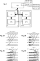
- the figure 1 is a block diagram of such a processor architecture. It comprises a generic central processing unit (CPU) 10 strongly coupled to a coprocessor 12 integrating hardware operators dedicated to the calculation of matrix products.
- CPU central processing unit
- coprocessor 12 integrating hardware operators dedicated to the calculation of matrix products.
- strong coupling is meant that the coprocessor obeys machine instructions cycle by cycle which are executed in the central unit and which are implemented by hardware execution units 14.
- certain machine instructions of the processor instruction set incorporate commands dedicated to the coprocessor.
- the execution unit configures the operation of the coprocessor by command lines CTRL.
- the coprocessor is wired to immediately obey the signals presented on these control lines.
- the coprocessor is an extension of the execution units 14 of the central unit, obeying an extension of a set of generic instructions of the processor.
- the central unit 10 can be of a generic type, making it possible in particular to execute an operating system or a program compiled from a language generic programming.
- the coprocessor 12 comprises hardware units of algebraic calculation 16, notably integrating hardware operators dedicated to the calculation of multiplication of matrices.
- the coprocessor also integrates its own set of working registers 18, independent of a classic set of registers 20 of the central unit 10.
- the registers 18 and 20 are connected to a shared memory 22 by a data bus D of N bits. Address and memory control buses, obeying conventional execution units of the central processing unit, are not shown.
- the registers 18 of the coprocessor have the same size N as the data bus and are configured to obey commands from an execution unit 14 of the central unit.
- Two matrices to be multiplied [a] and [b] are initially stored in shared memory 22.
- a matrix is stored by default by rows (so-called “row-major” format), namely that the elements of the same row are found at consecutive addresses, or by columns (so-called “column-major” format), ie the elements of the same column are found at consecutive addresses.
- the C programming language uses the first format, while the Fortran uses the second format.
- BLAS standard libraries of linear algebra
- the two matrices to be multiplied are stored in complementary formats, for example the first matrix [a] is stored in rows, while the second matrix [b] is stored in columns.
- the matrix [b] is thus stored in transposed form.
- the figure 1 illustrates the content of the memory for a matrix [a] of x + 1 rows and y + 1 columns and a matrix [b] of y + 1 rows and z + 1 columns.
- the matrix [b] having a number of rows equal to the number of columns of the matrix [a], can be multiplied by the matrix [a].
- the coprocessor 12 is designed to multiply, entirely wired, two sub-matrices of the source matrices, the first sub-matrix [A] having a fixed number Q of rows, and the second sub-matrix [B] having a fixed number columns which we will assume for the moment equal to Q.
- the remaining dimension of the sub-matrices which we will call hereinafter depth, is configurable according to the desired precision for the elements of the matrices.
- the multiplication of these sub-matrices therefore produces a result sub-matrix [C] of QxQ elements.
- the number Q determines the material resources necessary to carry out the multiplication.
- each sub-matrix to be multiplied is considered to have an overall size of N bits, namely the size of the data bus D, which will be assumed to be equal to 256 bits by way of example below.
- the sub-matrices have 4 rows or columns of 64-bit depth. This depth is occupied, depending on the application, by eight bytes, four 16-bit words, two 32-bit words, or one 64-bit word. These can be integers or fixed or floating point numbers.
- one objective is to supply the coprocessor with series of sub-matrices to be multiplied by fully exploiting the memory bus D.
- two readings would suffice to read a quantity of data corresponding to two sub- matrices.
- the organization of the source matrices in memory does not allow that directly in a general case. Indeed, 256 consecutive bits in memory cover data of consecutive rows (or columns) of any depth, and do not contain 4 aligned sub-rows (or sub-columns) which can form a sub-matrix.
- a register control unit of the coprocessor 12 is configured to divide the word W into K segments of N / K bits and write these segments respectively in the K designated registers. In other words, the word W is "scattered" across the registers. The position at which the segments are written to the designated registers is determined by the variant of the read-disperse instruction executed.
- FIGS. 2A to 2D illustrate the execution of variants of the read-disperse instruction on source matrices [a] and [b] of depth greater than 256 bits.
- the elements of the matrices are 16-bit words.
- a load.0 instruction is executed.
- the memory address conveyed in the instruction designates, for example, the first element of the first row of the matrix [a], namely the element a [0] [0].
- the word W0 returned on the bus therefore contains the elements a [0] [0] to a [0] [15].
- the variant of the instruction configures the registers V0 to V3 to receive the respective four segments of the word W0 in their first quarter.
- a load statement . 1 is executed.
- the memory address designates the element a [1] [0].
- the word W1 returned on the bus therefore contains the elements a [1] [0] to a [1] [15].
- the variant of the instruction configures the registers V0 to V3 to receive the respective four segments of the word W1 in their second quarter.
- a load statement . 2 is executed.
- the memory address designates the element a [2] [0].
- the word W2 returned on the bus therefore contains the elements a [2] [0] to a [2] [15].
- the variant of the instruction configures the registers V0 to V3 to receive the respective four segments of the word W2 in their third quarter.
- a load statement. 3 is finally executed.
- the memory address designates the element a [3] [0].
- the word W3 returned on the bus therefore contains the elements a [3] [0] to a [3] [15].
- the variant of the instruction configures the registers V0 to V3 to receive the respective four segments of the word W3 in their fourth quarter.
- each of the registers V0 to V3 contains a consecutive sub-matrix [A] of 4x4 16-bit words (also denoted 4x4x16) in the direction of the rows of the source matrix [a].
- the rows of each sub-matrix are contained in four respective segments of the corresponding register V.
- the registers V0 to V3, containing sub-matrices [A], will be designated VA0 to VA3.
- each of these registers receives a consecutive sub-matrix [B] of 4x4x16 in the direction of the columns of the source matrix [b].
- the columns of each sub-matrix are contained in four respective segments of the corresponding VB register.
- a register VAi contains four vectors A [0] to A [3] and a register VBj contains four vectors B [0] to B [3], each vector having four 16-bit components.
- the figure 3 is a block diagram of an embodiment of a hardware calculation unit 16 of the coprocessor, intended to carry out a multiplication of two sub-matrices [A] and [B] in response to a single dedicated machine instruction that the we will note mm4a.
- This embodiment corresponds to the example considered in Figures 2A to 2B , where the array elements are 16 bits in size.
- the calculation unit includes a matrix of 4x4 material operators of scalar product and accumulation denoted DP4A, where the number 4 designates the dimension of the vectors.
- a DP4A operator of row i and column j is wired to perform the dot product of vectors A [i] and B [j] contained in registers VA and VB respectively, and accumulate the dot product in a cell Cij of a sub -matrix result [C].
- the cell Cij can be all or part of an appropriately sized segment of a register of the coprocessor.
- a comfortable size is 64 bits, which implies four registers VCa to VCd to store the result sub-matrix [C].
- the registers VA, VB and VC are designated by an instruction mm4a being executed in the central unit 10, here the registers VA0, VB0 and VC0a-VC0d.
- the registers VC are configured to preserve the organization in Q segments of the registers VA and VB.
- Q 4 and each result element is coded on 64 bits
- each of the 4 segments of the registers VC contains a single element.
- the registers VC are organized so that the four segments of the same register store elements of different rows.
- the contents of the four registers VC can be transferred in memory in four cycles to addresses corresponding to the positions of the columns of the sub-matrix [C] in the complete result matrix [c], thus contributing to a result matrix [c] stored by columns (“column-major”).
- the VC registers could also be organized in a complementary manner so that the four segments of the same register store elements of different columns.
- the contents of the four registers VC can be transferred into memory in four cycles corresponding to the positions of the rows of the sub-matrix [C] in the complete result matrix [c], contributing to a result matrix [c] stored by rows ("row-major").
- each of the registers VCa, VCb, VCc, VCd can be stored in memory to contribute to a row of the result matrix [c] stored by rows (“row-major”).
- the figure 4 is a block diagram of a dot product operator DP4A of position (i, j) in the operator matrix.
- the operator processes the vectors A [i] and B [j]. More specifically, the operator comprises four 16-bit MUL multipliers each receiving a respective component (Ai0 to Ai3) of the vector A [i] as the first multiplicand, and the corresponding component (B0j to B3j) of the vector B [j] as second multiplicand.
- the four products, coded on 32 bits, are supplied to a multi-adder 40 connected to accumulate the sum of the products in a segment of register Cij of 64 bits.
- By “accumulate” we mean that the Cij segment receives the sum of the products and previous content of the Cij segment.
- Multi-adder 40 is thus wired to sum four 32-bit numbers and one 64-bit number.
- the unit of calculation of the figure 3 instantly produces the result matrix [C] in response to a mm4a instruction which designates the registers VA, VB and VC to be used.
- a calculation unit taking into account the propagation delays of the combinational logic, will take more than one clock cycle of the processor to establish the result.
- the calculation unit in particular each DP4A operator, is generally designed in a pipeline structure, meaning that the calculation is broken down into several stages synchronized on successive clock cycles, but that a new calculation can be initiated. ie execute a new mm4a instruction, at each clock cycle.
- a pipeline structure is less than optimal for making isolated calculations.
- the pipeline structure can be 100% efficient after an initial phase of priming the pipeline and before a final phase of emptying the pipeline.
- VLIW architecture Very Large Instruction Word
- the table 1 below presents a sequence of instructions which makes it possible to multiply a matrix [a] of 8x32 by a matrix [b] of 32x8 to provide a matrix [c] of 8x8 without dead time and by exploiting all the bandwidth of the memory bus and the computing unit in parallel. Instructions placed on the same line correspond to instructions executed in the same VLIW packet.
- the registers of the coprocessor are designated by Ax and By for the multiplicand sub-matrices and Cz for the result sub-matrix, knowing that all these registers, chosen from the set of registers 18 , are of the same nature.
- Phases 0 and 1 correspond to what has been described in relation to the Figures 2A-2D .
- registers C0 to C15 contain the matrix resulting from the multiplication, an 8x8x64 matrix.
- phases 6 to 9 re-use the registers C of phases 2 to 5, namely the same result sub-matrices c [0..3] [0..3], c [0..3] [4. .7], c [4..7] [0..3] and c [4..7] [4..7].
- one calculates the sub-matrices c [] [] only on the first half of the depth of the source matrices (elements 0 to 15).
- phases 6 to 9 we update the sub-matrices c [] [] with the influence of the second half of the depth of the source matrices (elements 16 to 31). This computation naturally extends to any depth by updating the sub-matrices c [] [] with the influence of the following slices of 256 bits in the depth of the matrices [a] and [b].
- the source matrices mentioned by way of example have a depth multiple of the width N of the memory bus.
- the read-disperse operations affecting the last part of the rows (or columns) read words of which a first part contains the end of the row (or column), and the second part contains unusable data. (either the start of a misaligned row or column, or arbitrary data after the end of the matrix).
- the data of the second part of the words are replaced by zeros, and the words thus readjusted are treated normally as explained above.
- the depth of the matrices varies according to the precision chosen for the elements.
- the elements can also be 8 or 32 bits without this affecting the organization of the source matrices in memory or their transfer in the registers of the coprocessor. Certain modifications can however be made in the calculation unit 16 of the coprocessor.
- the figure 5 is a block diagram of an embodiment of a calculation unit 16 of the coprocessor, intended to carry out a multiplication of two sub-matrices [A] and [B] of 8-bit elements in response to a single instruction dedicated machine which will be noted mm8a.
- the dot product operators here denoted DP8A, are then configured to simultaneously calculate eight products and their sum.
- the precision of the results is 32 bits instead of 64 bits, from which it results that only two registers VC0a and VC0b are required to store the result sub-matrix [C].
- the registers VC are organized so that each segment stores two row elements of the result sub-matrix.
- the register VC0a contains in its respective segments, the pairs (C00, C01), (C10, C11), (C20, C21) and (C30, C31).
- the contents of the two registers VC are not directly transferable in memory in the correct order to form a 4x4 sub-matrix of the result matrix [c].
- the instruction set of the processor is extended by an instruction complementary to the read-disperse instruction, which will be designated by gather-write instruction or “gather-store”.
- gather-write instruction or “gather-store”.
- the execution of this instruction by the central unit configures the coprocessor to concatenate on the memory bus Q segments taken from Q designated registers.
- the position of the segment in the registers is defined by a corresponding variant of the instruction.
- the word W0 contains the elements C00, C01 of the first segment of the register VC0a, followed by the elements C02, C03 of the first segment of the register VC0b, followed by the four elements of the first row of the second sub-matrix stored in the first segments of registers VC1a and VC1b (not shown).
- the three remaining cycles thus transfer the second to fourth rows of the two sub-matrices. Two adjacent sub-matrices are thus formed by rows in a result matrix stored by rows while fully occupying the bandwidth of the bus.
- the figure 6 is a block diagram of a DP8A dot product operator of position (i, j) in the operator matrix. It comprises eight multipliers of 8 bits each receiving a respective component (Ai0 to Ai7) of the vector A [i] as the first multiplicand, and the corresponding component (B0j to B7j) of the vector B [j] as the second multiplicand.
- the eight products, coded on 16 bits, are supplied to a multi-adder 40b connected to accumulate the sum of the products in a 32-bit Cij register segment.
- the transfer from memory to the registers of the coprocessor is always carried out in the same way, with a series of four read-disperse instructions.
- the register segments then contain vectors of two 32-bit elements.
- the dot product operators are then denoted DP2A and accumulate two 32-bit number products in a 64 or 128 bit register segment.
- the instruction of multiplication of matrices is then noted mm2a.
- the figure 7 is a block diagram of an embodiment of a scalar product operator configurable for processing matrix elements of adjustable precision among 8, 16 and 32 bits. It includes two 32-bit number multipliers, two multipliers 16-bit numbers and four 8-bit number multipliers, the outputs of which are supplied to a 40c multi-adder, connected to accumulate the sum of the products in a Cij register segment of 64 or 128 bits.
- the 32x32 multipliers are connected to process the first two components of the vectors, whatever their precision.
- the only two components of a 2x32 bit vector are applied to all input lines of 32x32 multipliers.
- the other multipliers produce a zero result.
- the 16x16 multipliers are connected to process the third and fourth components of 4x16 or 8x8 bit vectors.
- the first two components are applied respectively to the first 16 input lines of the two 32x32 multipliers, and the following two components are applied respectively to all the input lines of the two 16x16 multipliers.
- the first four components are applied respectively to the first 8 input lines of the two 32x32 multipliers and the two 16x16 multipliers, and the remaining components are applied respectively to all the input lines of the 8x8 multipliers.
- the organization of the connection of the inputs of the multipliers to the registers is determined by the nature of the instruction for multiplication of matrices executed, namely mm2a, mm4a or mm8a.
- the array elements can be integers or floating point numbers (in the latter case, 16 bit and 32 bit sizes are used instead).
- Multipliers and adders are configured accordingly. If we want to process whole numbers and floating point numbers, the multipliers will have a reconfigurable structure based on a floating point multiplication structure.
- the precision of the results could be 64 bits or 128 bits.
- a precision of 64 bits can suffice if we accept a certain level of error, in particular a saturation when processing whole numbers, or a rounding error when dealing with fixed or floating point numbers.
- the two source matrices to be multiplied had elements of the same precision.
- the architecture described also makes it possible to multiply mixed precision matrices. For example, in the case of a multiplication of a matrix [a] of 16-bit elements by a matrix [b] of 8-bit elements, the following operations are planned.
- registers A0-A3 are filled by a first series of four read-disperse instructions to contain four 4x4x16 sub-matrices taken in the first four rows of the source matrix [a].
- these matrices contain the rows a [0] [0..15] to a [3] [0..15].
- registers A4-A7 are filled by a second series of four read-disperse instructions to contain four 4x4x16 sub-matrices taken in the next four rows of the matrix [a].
- these matrices contain the rows a [4] [0..15] to a [7] [0..15].
- registers B0-B3 are filled by a third series of four read-disperse instructions to contain eight 4x4x8 sub-matrices taken in the first four columns of the matrix [b].
- these matrices contain columns b [0..31] [0] to b [0..31] [3].
- the two halves of register B0 contain two sub-matrices, one of which b [0..3] [0..3] can be multiplied with the sub-matrix a [0..3] [0..3] of register A0 to contribute to the result sub-matrix c [0..3] [0..3].
- the other sub-matrix b [4..7] [0..3] of the register B0 can be multiplied with the sub-matrix a [4..7] [0..3] of the register A4 to contribute to the result sub-matrix c [4..7] [0..3].
- the two halves of register B1 contain two sub-matrices which can be multiplied respectively with the sub-matrices of registers A1 and A5 to contribute respectively to the same sub-matrices result c [0..3] [0..3] and c [4..7] [0..3].
- the two halves of the register B2 respectively contain two sub-matrices to be multiplied with the sub-matrices of the registers A2 and A6
- the two halves of the register B3 respectively contain two sub-matrices to be multiplied with the sub-matrices of the registers A3 and A7, each time to contribute to the same result sub-matrices c [0..3] [0..3] and c [4..7] [0..3], that is to say without changing the VC registers during these operations.
- two variants of the mm4a multiplication operation can be used to be used in two consecutive cycles designating two different A registers (for example A0 and A4), a same corresponding B register (for example B0 ), and two sets of two C registers to hold the result.
- the two variants first configure the DP4A operators to use only the 8 least significant bits of the inputs B of the multipliers (called half-inputs).
- the first variant further reconfigures the operators to connect the 16 half-inputs of 8 bits to the first four bytes contained in each of the segments Bi0 to Bi3 of the register B0.
- the second variant reconfigures the operators to connect the 16 8-bit half-inputs to the last four bytes contained in each of the segments Bi0 to Bi3 of the register B0.
- the VB0 register is considered to be subdivided into two halves, each with 4 segments each containing a four-byte vector, and the DP4A dot product operators are organized into two 4x4 sub-matrices which simultaneously process the two respective halves of the VB0 register.
- a calculation unit comprising scalar product operators organized in a matrix RxQ with R> Q.
- Each register A then contains a sub-matrix of Q rows with elements of size N / Q bits
- each register B contains R / Q sub-matrices of Q columns with elements of size N / R bits, where N is the width of the memory bus and the size of the registers, and is divisible by Q and by R.
- Each multiplication instruction reads the contents of R / Q registers A and of a register B, to produce a sub-matrix of dimensions RxQ.
Landscapes
- Engineering & Computer Science (AREA)
- Physics & Mathematics (AREA)
- Theoretical Computer Science (AREA)
- General Physics & Mathematics (AREA)
- Software Systems (AREA)
- General Engineering & Computer Science (AREA)
- Mathematical Physics (AREA)
- Mathematical Analysis (AREA)
- Mathematical Optimization (AREA)
- Pure & Applied Mathematics (AREA)
- Computational Mathematics (AREA)
- Data Mining & Analysis (AREA)
- Computing Systems (AREA)
- Algebra (AREA)
- Databases & Information Systems (AREA)
- Advance Control (AREA)
- Complex Calculations (AREA)
Applications Claiming Priority (1)
| Application Number | Priority Date | Filing Date | Title |
|---|---|---|---|
| FR1873594A FR3090932B1 (fr) | 2018-12-20 | 2018-12-20 | Système de multiplication de matrices par blocs |
Publications (3)
| Publication Number | Publication Date |
|---|---|
| EP3671488A1 true EP3671488A1 (de) | 2020-06-24 |
| EP3671488C0 EP3671488C0 (de) | 2024-04-17 |
| EP3671488B1 EP3671488B1 (de) | 2024-04-17 |
Family
ID=66641077
Family Applications (1)
| Application Number | Title | Priority Date | Filing Date |
|---|---|---|---|
| EP19214860.9A Active EP3671488B1 (de) | 2018-12-20 | 2019-12-10 | System zur blockweisen vervielfältigung von matrizen |
Country Status (4)
| Country | Link |
|---|---|
| US (1) | US11169808B2 (de) |
| EP (1) | EP3671488B1 (de) |
| CN (1) | CN111353126B (de) |
| FR (1) | FR3090932B1 (de) |
Cited By (2)
| Publication number | Priority date | Publication date | Assignee | Title |
|---|---|---|---|---|
| CN115114085A (zh) * | 2022-06-24 | 2022-09-27 | 山东云海国创云计算装备产业创新中心有限公司 | 一种数据恢复方法、装置、计算机设备及存储介质 |
| CN117093816A (zh) * | 2023-10-19 | 2023-11-21 | 上海登临科技有限公司 | 矩阵乘运算方法、装置和电子设备 |
Families Citing this family (14)
| Publication number | Priority date | Publication date | Assignee | Title |
|---|---|---|---|---|
| US11169776B2 (en) * | 2019-06-28 | 2021-11-09 | Intel Corporation | Decomposed floating point multiplication |
| US11054998B1 (en) | 2019-12-12 | 2021-07-06 | Facebook, Inc. | High bandwidth memory system with distributed request broadcasting masters |
| CN113918879A (zh) * | 2020-07-08 | 2022-01-11 | 华为技术有限公司 | 矩阵运算的方法和加速器 |
| CN112506567B (zh) * | 2020-11-27 | 2022-11-04 | 海光信息技术股份有限公司 | 数据读取方法和数据读取电路 |
| CN112434256B (zh) * | 2020-12-03 | 2022-09-13 | 海光信息技术股份有限公司 | 矩阵乘法器和处理器 |
| CN112506468B (zh) * | 2020-12-09 | 2023-04-28 | 上海交通大学 | 支持高吞吐多精度乘法运算的risc-v通用处理器 |
| FR3118505B1 (fr) | 2020-12-31 | 2024-01-19 | Kalray | Système de traitement de matrices par plusieurs processeurs simultanément |
| US12002453B2 (en) * | 2021-03-25 | 2024-06-04 | Beijing Transtreams Technology Co. Ltd. | Methods and devices for irregular pruning for automatic speech recognition |
| CN114579929B (zh) * | 2022-03-14 | 2023-08-08 | 海飞科(南京)信息技术有限公司 | 加速器执行的方法和电子设备 |
| CN115373630B (zh) * | 2022-10-24 | 2022-12-20 | 北京麟卓信息科技有限公司 | 一种面向异构芯片的矩阵乘法运算过程优化方法 |
| CN116304513A (zh) * | 2023-03-16 | 2023-06-23 | 中国人民解放军国防科技大学 | 一种48位混合精度矩阵向量乘法实现方法及装置 |
| CN117454068B (zh) * | 2023-11-10 | 2025-01-24 | 上海壁仞科技股份有限公司 | 实现矩阵乘运算的方法和计算设备 |
| CN118227948B (zh) * | 2024-05-24 | 2024-08-06 | 北京壁仞科技开发有限公司 | 人工智能芯片、操作方法和机器可读存储介质 |
| CN120337997B (zh) * | 2025-06-17 | 2025-10-21 | 浪潮电子信息产业股份有限公司 | 基于人工智能模型的运行方法、装置、设备、介质和产品 |
Family Cites Families (14)
| Publication number | Priority date | Publication date | Assignee | Title |
|---|---|---|---|---|
| JP2556182B2 (ja) * | 1990-08-29 | 1996-11-20 | 三菱電機株式会社 | デ−タ処理装置 |
| US6170001B1 (en) * | 1998-05-27 | 2001-01-02 | Arm Limited | System for transfering format data from format register to memory wherein format data indicating the distribution of single or double precision data type in the register bank |
| US20040122887A1 (en) * | 2002-12-20 | 2004-06-24 | Macy William W. | Efficient multiplication of small matrices using SIMD registers |
| US20060179273A1 (en) * | 2005-02-09 | 2006-08-10 | Advanced Micro Devices, Inc. | Data processor adapted for efficient digital signal processing and method therefor |
| US7627735B2 (en) * | 2005-10-21 | 2009-12-01 | Intel Corporation | Implementing vector memory operations |
| EP2150889A1 (de) * | 2007-04-10 | 2010-02-10 | Cambridge Consultants Limited | Datenverarbeitungsvorrichtung |
| US8285766B2 (en) * | 2007-05-23 | 2012-10-09 | The Trustees Of Princeton University | Microprocessor shifter circuits utilizing butterfly and inverse butterfly routing circuits, and control circuits therefor |
| CN101609715B (zh) * | 2009-05-11 | 2012-09-05 | 中国人民解放军国防科学技术大学 | 行列访问端口分离的矩阵寄存器文件 |
| US9960917B2 (en) * | 2011-12-22 | 2018-05-01 | Intel Corporation | Matrix multiply accumulate instruction |
| US10055225B2 (en) * | 2011-12-23 | 2018-08-21 | Intel Corporation | Multi-register scatter instruction |
| CN103631761B (zh) * | 2012-08-29 | 2018-02-27 | 睿励科学仪器(上海)有限公司 | 并行处理架构进行矩阵运算并用于严格波耦合分析的方法 |
| US9384168B2 (en) * | 2013-06-11 | 2016-07-05 | Analog Devices Global | Vector matrix product accelerator for microprocessor integration |
| US9710279B2 (en) * | 2014-09-26 | 2017-07-18 | Intel Corporation | Method and apparatus for speculative vectorization |
| US9910827B2 (en) * | 2016-07-01 | 2018-03-06 | Hewlett Packard Enterprise Development Lp | Vector-matrix multiplications involving negative values |
-
2018
- 2018-12-20 FR FR1873594A patent/FR3090932B1/fr active Active
-
2019
- 2019-12-10 EP EP19214860.9A patent/EP3671488B1/de active Active
- 2019-12-20 US US16/724,106 patent/US11169808B2/en active Active
- 2019-12-20 CN CN201911323478.7A patent/CN111353126B/zh active Active
Non-Patent Citations (3)
| Title |
|---|
| ANDREAS HEHN: "HIGH THROUGHPUT WITH GPUS", 19 November 2018 (2018-11-19), XP055633072, Retrieved from the Internet <URL:https://indico.cern.ch/event/764011/contributions/3214768/attachments/1755004/2845106/RAPID_workshop_20181119.pdf> [retrieved on 20191016] * |
| JIAJIA LI ET AL: "An optimized large-scale hybrid DGEMM design for CPUs and ATI GPUs", PROCEEDING ICS '12 PROCEEDINGS OF THE 26TH ACM INTERNATIONAL CONFERENCE ON SUPERCOMPUTING, 25 June 2012 (2012-06-25), pages 377, XP055632925, ISBN: 978-1-4503-1316-2, DOI: 10.1145/2304576.2304626 * |
| MINSEOK LEE: "Turing Architecture and CUDA 10 New Features", 7 November 2018 (2018-11-07), XP055633075, Retrieved from the Internet <URL:http://on-demand.gputechconf.com/gtc-kr/2018/pdf/HPC_Minseok_Lee_NVIDIA.pdf> [retrieved on 20191016] * |
Cited By (3)
| Publication number | Priority date | Publication date | Assignee | Title |
|---|---|---|---|---|
| CN115114085A (zh) * | 2022-06-24 | 2022-09-27 | 山东云海国创云计算装备产业创新中心有限公司 | 一种数据恢复方法、装置、计算机设备及存储介质 |
| CN117093816A (zh) * | 2023-10-19 | 2023-11-21 | 上海登临科技有限公司 | 矩阵乘运算方法、装置和电子设备 |
| CN117093816B (zh) * | 2023-10-19 | 2024-01-19 | 上海登临科技有限公司 | 矩阵乘运算方法、装置和电子设备 |
Also Published As
| Publication number | Publication date |
|---|---|
| US11169808B2 (en) | 2021-11-09 |
| US20200201642A1 (en) | 2020-06-25 |
| CN111353126B (zh) | 2025-02-18 |
| EP3671488C0 (de) | 2024-04-17 |
| EP3671488B1 (de) | 2024-04-17 |
| CN111353126A (zh) | 2020-06-30 |
| FR3090932A1 (fr) | 2020-06-26 |
| FR3090932B1 (fr) | 2022-05-27 |
Similar Documents
| Publication | Publication Date | Title |
|---|---|---|
| EP3671488B1 (de) | System zur blockweisen vervielfältigung von matrizen | |
| US8346833B2 (en) | Filter and method for filtering | |
| US11983616B2 (en) | Methods and apparatus for constructing digital circuits for performing matrix operations | |
| EP0329023A2 (de) | Einrichtung zur Ausführung einer digitalen Signalverarbeitung einschliesslich Wurzel-4-Schnellen Fourier-Transformationsschmetterlingsoperationen | |
| EP3084588B1 (de) | Signalverarbeitungsmodul, insbesondere für neuronales netzwerk und neuronale schaltung | |
| EP0558125B1 (de) | Neuronaler Prozessor mit verteilten synaptischen Zellen | |
| BE897441A (fr) | Calculateur associatif permettant une multiplication rapide | |
| NL8304186A (nl) | Geintegreerde processor voor het verwerken van woordsgewijze ontvangbare informatie. | |
| EP0171305B1 (de) | Rechenschaltung für die diskrete Fouriertransformation | |
| EP4193358A1 (de) | Rekonfigurierbares speichermodul zur implementierung von rechenoperationen | |
| EP0275765A1 (de) | Integrierter Schaltkreis für Digitalsignalverarbeitung | |
| EP0817006A2 (de) | Parallele Multiplizier-Akkumulier-Matrix-Schaltung | |
| EP0018298A1 (de) | Verfahren zum Ermitteln eines numerischen Rechenergebnisses in Gleitkommadarstellung mit der Anzahl der richtigen signifikativen Ziffern und numerische Recheneinrichtung zur Durchführung dieses Verfahrens | |
| EP0088544A1 (de) | Index limitierter kontinuierlich arbeitender Vektor-Prozessor | |
| FR2569288A1 (fr) | Dispositif de calcul d'adresse pour un appareil de traitement numerique | |
| FR2637707A1 (fr) | Circuit diviseur calculant un quotient de k chiffres de base m en k cycles machine | |
| FR3118505A1 (fr) | Système de traitement de matrices par plusieurs processeurs simultanément | |
| FR3101980A1 (fr) | Processeur | |
| EP0397807A1 (de) | Vorrichtung zum gleichzeitigen filtrieren und wiederbemustern von rechnerdaten | |
| EP2315085B1 (de) | Berichtigungsvorrichtung von Einstellwerten, und System zur Erzeugung von Gradienten, das eine solche Vorrichtung umfasst | |
| EP0239634A1 (de) | Mehrzonaler prozessor | |
| FR2652175A1 (fr) | Dispositif de conversion de nombres. | |
| WO2000026790A1 (fr) | Memoire a acces vectoriel | |
| EP0927928B1 (de) | Verbessertes Verfahren zum Erzeugen eines Parameters J0 bezüglich der Verwendung von modularen Operationen nach der Montgomery-Methode | |
| EP0291613A1 (de) | Prozessor mit einer Mehrheit von seriell geschalteten Stufen |
Legal Events
| Date | Code | Title | Description |
|---|---|---|---|
| PUAI | Public reference made under article 153(3) epc to a published international application that has entered the european phase |
Free format text: ORIGINAL CODE: 0009012 |
|
| STAA | Information on the status of an ep patent application or granted ep patent |
Free format text: STATUS: THE APPLICATION HAS BEEN PUBLISHED |
|
| AK | Designated contracting states |
Kind code of ref document: A1 Designated state(s): AL AT BE BG CH CY CZ DE DK EE ES FI FR GB GR HR HU IE IS IT LI LT LU LV MC MK MT NL NO PL PT RO RS SE SI SK SM TR |
|
| AX | Request for extension of the european patent |
Extension state: BA ME |
|
| STAA | Information on the status of an ep patent application or granted ep patent |
Free format text: STATUS: REQUEST FOR EXAMINATION WAS MADE |
|
| 17P | Request for examination filed |
Effective date: 20201211 |
|
| RBV | Designated contracting states (corrected) |
Designated state(s): AL AT BE BG CH CY CZ DE DK EE ES FI FR GB GR HR HU IE IS IT LI LT LU LV MC MK MT NL NO PL PT RO RS SE SI SK SM TR |
|
| REG | Reference to a national code |
Ref country code: DE Ref legal event code: R079 Free format text: PREVIOUS MAIN CLASS: G06F0017160000 Ref document number: 602019050367 Country of ref document: DE Ipc: G06F0012060000 |
|
| GRAP | Despatch of communication of intention to grant a patent |
Free format text: ORIGINAL CODE: EPIDOSNIGR1 |
|
| STAA | Information on the status of an ep patent application or granted ep patent |
Free format text: STATUS: GRANT OF PATENT IS INTENDED |
|
| RIC1 | Information provided on ipc code assigned before grant |
Ipc: G06F 17/16 20060101ALI20231130BHEP Ipc: G06F 12/06 20060101AFI20231130BHEP |
|
| INTG | Intention to grant announced |
Effective date: 20231222 |
|
| GRAS | Grant fee paid |
Free format text: ORIGINAL CODE: EPIDOSNIGR3 |
|
| GRAA | (expected) grant |
Free format text: ORIGINAL CODE: 0009210 |
|
| STAA | Information on the status of an ep patent application or granted ep patent |
Free format text: STATUS: THE PATENT HAS BEEN GRANTED |
|
| AK | Designated contracting states |
Kind code of ref document: B1 Designated state(s): AL AT BE BG CH CY CZ DE DK EE ES FI FR GB GR HR HU IE IS IT LI LT LU LV MC MK MT NL NO PL PT RO RS SE SI SK SM TR |
|
| REG | Reference to a national code |
Ref country code: GB Ref legal event code: FG4D Free format text: NOT ENGLISH |
|
| REG | Reference to a national code |
Ref country code: CH Ref legal event code: EP |
|
| REG | Reference to a national code |
Ref country code: DE Ref legal event code: R096 Ref document number: 602019050367 Country of ref document: DE |
|
| REG | Reference to a national code |
Ref country code: IE Ref legal event code: FG4D Free format text: LANGUAGE OF EP DOCUMENT: FRENCH |
|
| U01 | Request for unitary effect filed |
Effective date: 20240507 |
|
| U07 | Unitary effect registered |
Designated state(s): AT BE BG DE DK EE FI FR IT LT LU LV MT NL PT SE SI Effective date: 20240521 |
|
| PG25 | Lapsed in a contracting state [announced via postgrant information from national office to epo] |
Ref country code: IS Free format text: LAPSE BECAUSE OF FAILURE TO SUBMIT A TRANSLATION OF THE DESCRIPTION OR TO PAY THE FEE WITHIN THE PRESCRIBED TIME-LIMIT Effective date: 20240817 |
|
| PG25 | Lapsed in a contracting state [announced via postgrant information from national office to epo] |
Ref country code: HR Free format text: LAPSE BECAUSE OF FAILURE TO SUBMIT A TRANSLATION OF THE DESCRIPTION OR TO PAY THE FEE WITHIN THE PRESCRIBED TIME-LIMIT Effective date: 20240417 |
|
| PG25 | Lapsed in a contracting state [announced via postgrant information from national office to epo] |
Ref country code: GR Free format text: LAPSE BECAUSE OF FAILURE TO SUBMIT A TRANSLATION OF THE DESCRIPTION OR TO PAY THE FEE WITHIN THE PRESCRIBED TIME-LIMIT Effective date: 20240718 |
|
| PG25 | Lapsed in a contracting state [announced via postgrant information from national office to epo] |
Ref country code: ES Free format text: LAPSE BECAUSE OF FAILURE TO SUBMIT A TRANSLATION OF THE DESCRIPTION OR TO PAY THE FEE WITHIN THE PRESCRIBED TIME-LIMIT Effective date: 20240417 |
|
| PG25 | Lapsed in a contracting state [announced via postgrant information from national office to epo] |
Ref country code: PL Free format text: LAPSE BECAUSE OF FAILURE TO SUBMIT A TRANSLATION OF THE DESCRIPTION OR TO PAY THE FEE WITHIN THE PRESCRIBED TIME-LIMIT Effective date: 20240417 |
|
| PG25 | Lapsed in a contracting state [announced via postgrant information from national office to epo] |
Ref country code: PL Free format text: LAPSE BECAUSE OF FAILURE TO SUBMIT A TRANSLATION OF THE DESCRIPTION OR TO PAY THE FEE WITHIN THE PRESCRIBED TIME-LIMIT Effective date: 20240417 Ref country code: NO Free format text: LAPSE BECAUSE OF FAILURE TO SUBMIT A TRANSLATION OF THE DESCRIPTION OR TO PAY THE FEE WITHIN THE PRESCRIBED TIME-LIMIT Effective date: 20240717 Ref country code: IS Free format text: LAPSE BECAUSE OF FAILURE TO SUBMIT A TRANSLATION OF THE DESCRIPTION OR TO PAY THE FEE WITHIN THE PRESCRIBED TIME-LIMIT Effective date: 20240817 Ref country code: HR Free format text: LAPSE BECAUSE OF FAILURE TO SUBMIT A TRANSLATION OF THE DESCRIPTION OR TO PAY THE FEE WITHIN THE PRESCRIBED TIME-LIMIT Effective date: 20240417 Ref country code: GR Free format text: LAPSE BECAUSE OF FAILURE TO SUBMIT A TRANSLATION OF THE DESCRIPTION OR TO PAY THE FEE WITHIN THE PRESCRIBED TIME-LIMIT Effective date: 20240718 Ref country code: ES Free format text: LAPSE BECAUSE OF FAILURE TO SUBMIT A TRANSLATION OF THE DESCRIPTION OR TO PAY THE FEE WITHIN THE PRESCRIBED TIME-LIMIT Effective date: 20240417 Ref country code: RS Free format text: LAPSE BECAUSE OF FAILURE TO SUBMIT A TRANSLATION OF THE DESCRIPTION OR TO PAY THE FEE WITHIN THE PRESCRIBED TIME-LIMIT Effective date: 20240717 |
|
| REG | Reference to a national code |
Ref country code: DE Ref legal event code: R097 Ref document number: 602019050367 Country of ref document: DE |
|
| U20 | Renewal fee for the european patent with unitary effect paid |
Year of fee payment: 6 Effective date: 20241216 |
|
| PG25 | Lapsed in a contracting state [announced via postgrant information from national office to epo] |
Ref country code: CZ Free format text: LAPSE BECAUSE OF FAILURE TO SUBMIT A TRANSLATION OF THE DESCRIPTION OR TO PAY THE FEE WITHIN THE PRESCRIBED TIME-LIMIT Effective date: 20240417 |
|
| PG25 | Lapsed in a contracting state [announced via postgrant information from national office to epo] |
Ref country code: SK Free format text: LAPSE BECAUSE OF FAILURE TO SUBMIT A TRANSLATION OF THE DESCRIPTION OR TO PAY THE FEE WITHIN THE PRESCRIBED TIME-LIMIT Effective date: 20240417 Ref country code: RO Free format text: LAPSE BECAUSE OF FAILURE TO SUBMIT A TRANSLATION OF THE DESCRIPTION OR TO PAY THE FEE WITHIN THE PRESCRIBED TIME-LIMIT Effective date: 20240417 |
|
| PG25 | Lapsed in a contracting state [announced via postgrant information from national office to epo] |
Ref country code: SM Free format text: LAPSE BECAUSE OF FAILURE TO SUBMIT A TRANSLATION OF THE DESCRIPTION OR TO PAY THE FEE WITHIN THE PRESCRIBED TIME-LIMIT Effective date: 20240417 |
|
| PG25 | Lapsed in a contracting state [announced via postgrant information from national office to epo] |
Ref country code: SM Free format text: LAPSE BECAUSE OF FAILURE TO SUBMIT A TRANSLATION OF THE DESCRIPTION OR TO PAY THE FEE WITHIN THE PRESCRIBED TIME-LIMIT Effective date: 20240417 Ref country code: SK Free format text: LAPSE BECAUSE OF FAILURE TO SUBMIT A TRANSLATION OF THE DESCRIPTION OR TO PAY THE FEE WITHIN THE PRESCRIBED TIME-LIMIT Effective date: 20240417 Ref country code: RO Free format text: LAPSE BECAUSE OF FAILURE TO SUBMIT A TRANSLATION OF THE DESCRIPTION OR TO PAY THE FEE WITHIN THE PRESCRIBED TIME-LIMIT Effective date: 20240417 Ref country code: CZ Free format text: LAPSE BECAUSE OF FAILURE TO SUBMIT A TRANSLATION OF THE DESCRIPTION OR TO PAY THE FEE WITHIN THE PRESCRIBED TIME-LIMIT Effective date: 20240417 |
|
| PLBE | No opposition filed within time limit |
Free format text: ORIGINAL CODE: 0009261 |
|
| STAA | Information on the status of an ep patent application or granted ep patent |
Free format text: STATUS: NO OPPOSITION FILED WITHIN TIME LIMIT |
|
| 26N | No opposition filed |
Effective date: 20250120 |
|
| PG25 | Lapsed in a contracting state [announced via postgrant information from national office to epo] |
Ref country code: MC Free format text: LAPSE BECAUSE OF FAILURE TO SUBMIT A TRANSLATION OF THE DESCRIPTION OR TO PAY THE FEE WITHIN THE PRESCRIBED TIME-LIMIT Effective date: 20240417 |
|
| PG25 | Lapsed in a contracting state [announced via postgrant information from national office to epo] |
Ref country code: IE Free format text: LAPSE BECAUSE OF NON-PAYMENT OF DUE FEES Effective date: 20241210 |
|
| REG | Reference to a national code |
Ref country code: CH Ref legal event code: U11 Free format text: ST27 STATUS EVENT CODE: U-0-0-U10-U11 (AS PROVIDED BY THE NATIONAL OFFICE) Effective date: 20260108 |
|
| PGFP | Annual fee paid to national office [announced via postgrant information from national office to epo] |
Ref country code: GB Payment date: 20251229 Year of fee payment: 7 |
|
| U20 | Renewal fee for the european patent with unitary effect paid |
Year of fee payment: 7 Effective date: 20251215 |
|
| PGFP | Annual fee paid to national office [announced via postgrant information from national office to epo] |
Ref country code: CH Payment date: 20260108 Year of fee payment: 7 |