EP3671488B1 - System zur blockweisen vervielfältigung von matrizen - Google Patents
System zur blockweisen vervielfältigung von matrizen Download PDFInfo
- Publication number
- EP3671488B1 EP3671488B1 EP19214860.9A EP19214860A EP3671488B1 EP 3671488 B1 EP3671488 B1 EP 3671488B1 EP 19214860 A EP19214860 A EP 19214860A EP 3671488 B1 EP3671488 B1 EP 3671488B1
- Authority
- EP
- European Patent Office
- Prior art keywords
- registers
- instruction
- submatrix
- segments
- operand
- Prior art date
- Legal status (The legal status is an assumption and is not a legal conclusion. Google has not performed a legal analysis and makes no representation as to the accuracy of the status listed.)
- Active
Links
Images


Classifications
-
- G—PHYSICS
- G06—COMPUTING OR CALCULATING; COUNTING
- G06F—ELECTRIC DIGITAL DATA PROCESSING
- G06F9/00—Arrangements for program control, e.g. control units
- G06F9/06—Arrangements for program control, e.g. control units using stored programs, i.e. using an internal store of processing equipment to receive or retain programs
- G06F9/30—Arrangements for executing machine instructions, e.g. instruction decode
- G06F9/30145—Instruction analysis, e.g. decoding, instruction word fields
-
- G—PHYSICS
- G06—COMPUTING OR CALCULATING; COUNTING
- G06F—ELECTRIC DIGITAL DATA PROCESSING
- G06F17/00—Digital computing or data processing equipment or methods, specially adapted for specific functions
- G06F17/10—Complex mathematical operations
- G06F17/16—Matrix or vector computation, e.g. matrix-matrix or matrix-vector multiplication, matrix factorization
-
- G—PHYSICS
- G06—COMPUTING OR CALCULATING; COUNTING
- G06F—ELECTRIC DIGITAL DATA PROCESSING
- G06F12/00—Accessing, addressing or allocating within memory systems or architectures
- G06F12/02—Addressing or allocation; Relocation
- G06F12/06—Addressing a physical block of locations, e.g. base addressing, module addressing, memory dedication
- G06F12/0607—Interleaved addressing
-
- G—PHYSICS
- G06—COMPUTING OR CALCULATING; COUNTING
- G06F—ELECTRIC DIGITAL DATA PROCESSING
- G06F7/00—Methods or arrangements for processing data by operating upon the order or content of the data handled
- G06F7/38—Methods or arrangements for performing computations using exclusively denominational number representation, e.g. using binary, ternary, decimal representation
- G06F7/48—Methods or arrangements for performing computations using exclusively denominational number representation, e.g. using binary, ternary, decimal representation using non-contact-making devices, e.g. tube, solid state device; using unspecified devices
- G06F7/52—Multiplying; Dividing
- G06F7/523—Multiplying only
-
- G—PHYSICS
- G06—COMPUTING OR CALCULATING; COUNTING
- G06F—ELECTRIC DIGITAL DATA PROCESSING
- G06F9/00—Arrangements for program control, e.g. control units
- G06F9/06—Arrangements for program control, e.g. control units using stored programs, i.e. using an internal store of processing equipment to receive or retain programs
- G06F9/30—Arrangements for executing machine instructions, e.g. instruction decode
- G06F9/30098—Register arrangements
- G06F9/30101—Special purpose registers
-
- G—PHYSICS
- G06—COMPUTING OR CALCULATING; COUNTING
- G06F—ELECTRIC DIGITAL DATA PROCESSING
- G06F9/00—Arrangements for program control, e.g. control units
- G06F9/06—Arrangements for program control, e.g. control units using stored programs, i.e. using an internal store of processing equipment to receive or retain programs
- G06F9/46—Multiprogramming arrangements
- G06F9/48—Program initiating; Program switching, e.g. by interrupt
- G06F9/4806—Task transfer initiation or dispatching
- G06F9/4843—Task transfer initiation or dispatching by program, e.g. task dispatcher, supervisor, operating system
- G06F9/485—Task life-cycle, e.g. stopping, restarting, resuming execution
-
- G—PHYSICS
- G06—COMPUTING OR CALCULATING; COUNTING
- G06F—ELECTRIC DIGITAL DATA PROCESSING
- G06F9/00—Arrangements for program control, e.g. control units
- G06F9/06—Arrangements for program control, e.g. control units using stored programs, i.e. using an internal store of processing equipment to receive or retain programs
- G06F9/46—Multiprogramming arrangements
- G06F9/54—Interprogram communication
- G06F9/544—Buffers; Shared memory; Pipes
Definitions
- the invention relates to the multiplication of matrices of numbers represented digitally, in particular to processors assisted by hardware accelerators specialized for matrix operations.
- the multiplication of large matrices is generally carried out in blocks, that is to say by passing through a decomposition of the matrices into sub-matrices of size adapted to the computing resources.
- the accelerators are thus designed to efficiently calculate the products of these sub-matrices.
- NVidia offers in its Volta graphics processor hardware operators called tensor cores, which each monopolize the resources of several graphics cores of the processor to carry out in parallel numerous calculations involved in the multiplication of sub-matrices.
- NVidia also offers in its integrated Xavier processor an NVDLA unit (“NVidia Deep Learning Accelerator”), independent of graphics cores with tensor cores, and specialized in accelerating neural inference.
- NVidia Deep Learning Accelerator NVidia Deep Learning Accelerator
- the ICS conference article from 2012 entitled “An Optimized Large-Scale Hybrid DGEMM design for CPUs and ATI GPUs" by JIAJIA LI ET AL, discloses a method for multiplying matrices loaded into a local memory partitioned into several banks.
- Such an accelerator is said to be “loosely coupled” in that it receives tasks to be performed in batches prepared by a host processor, and then manages the tasks independently of the host processor, including access to a shared memory to read the data. matrices.
- the accelerator and host processor thus operate asynchronously, such that the host processor and accelerator compete for memory accesses and must synchronize regularly for the host processor to retrieve task results and communicate new tasks .
- the method may further comprise the steps of receiving in a central processing unit of a processor a read-scatter machine instruction; in response to the read-disperse instruction, delegate step c) to a coprocessor coupled to the central processing unit, the position of the segments and the registers being designated by reading-scattering instruction; receive in the central processing unit a submatrix multiplication machine instruction; and in response to the submatrix multiplication instruction, delegate step g) to the coprocessor.
- the processing unit and the coprocessor can be coupled according to a VLIW architecture, the method comprising a step of simultaneous execution of a read-disperse instruction and a submatrix multiplication instruction, contained in the same packet of instructions received by the central processing unit, from which it results that the read-disperse instruction prepares a next operand submatrix while the submatrix multiplication instruction operates on current operand submatrixes.
- the hardware operator may be configured to accumulate each dot product in a respective segment of a destination register designated by the instruction, with the previous contents of the respective segment, the method comprising the steps of executing the sub multiplication instruction -matrices R times by designating each time a different pair of operand registers of the same rank among the R first registers and the Q second registers, and the same set of destination registers.
- each source matrix can have a configurable precision of 8, 16 and 32 bits.
- a processor comprising an N-bit data bus configured to access a memory; a central processing unit connected to the data bus; a coprocessor coupled to the central processing unit, comprising N-bit working registers; an instruction processing unit in the central processing unit, configured to, in response to a read-disperse machine instruction received by the central processing unit, read access to a memory address and delegate to the coprocessor the processing of the corresponding word of N bits arriving on the data bus; a register control unit in the coprocessor, configured by the central processing unit in response to the read-disperse instruction, to divide the word arriving on the data bus into K segments and write the K segments at the same position in K respective registers, the position and registers being designated by the read-scatter instruction.
- the coprocessor may include a matrix of hardware dot product operators, each operator configured to simultaneously perform the dot product of two vectors contained in two segments of two respective operand registers, the ranks of the two segments in the operand registers being fixed by the position of the operator in the operator matrix, and the operand registers being designated by a sub-matrix multiplication machine instruction received by the central unit, from which it results that the operand registers contain respective operand sub-matrices, and the operator matrix produces a result submatrix.
- the operators can be configured to accumulate the dot products in respective segments of destination registers designated by the submatrix multiplication instruction.
- each operand submatrix can have a configurable precision of 8, 16 and 32 bits.
- Hardware accelerators dedicated to matrix multiplication face difficulties related to feeding the accelerator's calculation units with matrix data stored in shared memory, without causing a starvation of the calculation units or under-utilization. operation of these units.
- the format in which data is stored in memory may be unsuitable for the format required by the computing units, so latency and data buffers may be introduced to reorder the data.
- a processor architecture incorporating a strongly coupled coprocessor, having its own working registers, and a particular mechanism for transferring data between the memory and the registers of the coprocessor.
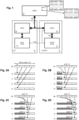
- FIG. 1 is a block diagram of such a processor architecture. It includes a generic central processing unit (CPU) 10 strongly coupled to a coprocessor 12 integrating hardware operators dedicated to the calculation of matrix products.
- CPU central processing unit
- coprocessor 12 integrating hardware operators dedicated to the calculation of matrix products.
- strong coupling we mean that the coprocessor obeys cycle by cycle machine instructions which are executed in the central unit and which are implemented by hardware execution units 14.
- some machine instructions in the processor's instruction set incorporate commands dedicated to the coprocessor.
- the execution unit configures the operation of the coprocessor by command lines CTRL.
- the coprocessor is wired to immediately obey signals presented on these command lines.
- the coprocessor is an extension of the execution units 14 of the central processing unit, obeying an extension of a set of generic instructions of the processor.
- the central unit 10 can be of a generic type, making it possible in particular to execute an operating system or a program compiled from a language generic programming.
- the coprocessor 12 includes hardware algebraic calculation units 16, integrating in particular hardware operators dedicated to the calculation of matrix multiplications.
- the coprocessor further integrates its own set of working registers 18, independent of a classic set of registers 20 of the central unit 10.
- Registers 18 and 20 are connected to a shared memory 22 by a data bus D of N bits. Address and memory control buses, obeying conventional execution units of the central processing unit, are not shown.
- the registers 18 of the coprocessor have the same size N as the data bus and are configured to obey commands from an execution unit 14 of the central processing unit.
- Two matrices to multiply [a] and [b] are initially stored in shared memory 22.
- a matrix is stored by default in rows (known as “row-major” format), i.e. the elements of the same row are found at consecutive addresses, or by columns (so-called “column-major” format), i.e. the elements of the same column are found at consecutive addresses.
- the C programming language uses the first format, while Fortran uses the second format.
- BLAS standard linear algebra libraries used in these programming languages provide transposition parameters to pass a matrix from one format to another according to the needs of the calculations.
- the two matrices to be multiplied are stored in complementary formats, for example the first matrix [a] is stored in rows, while the second matrix [b] is stored in columns.
- the matrix [b] is thus stored in transposed form.
- FIG 1 illustrates the memory contents for a matrix [a] of x+1 rows and y+1 columns and a matrix [b] of y+1 rows and z+1 columns.
- the matrix [b] having a number of rows equal to the number of columns of the matrix [a], can be multiplied by the matrix [a].
- the coprocessor 12 is designed to multiply, in a fully wired manner, two sub-matrices of the source matrices, the first sub-matrix [A] having a fixed number Q of rows, and the second sub-matrix [B] having a fixed number of columns which we will assume for the moment equal to Q.
- the remaining dimension of the sub-matrices which we will hereafter call depth, is configurable according to the precision desired for the elements of the matrices. The multiplication of these submatrices therefore produces a result submatrix [C] of Q ⁇ Q elements.
- the number Q determines the hardware resources needed to perform the multiplication.
- each submatrix to be multiplied is considered to have an overall size of N bits, namely the size of the data bus D, which will be assumed to be equal to 256 bits for example in the following.
- the submatrices have 4 rows or columns of 64 bits depth. This depth is occupied, depending on the applications, by eight bytes, four 16-bit words, two 32-bit words, or one 64-bit word. These can be integers or fixed or floating point numbers.
- an objective is to supply the coprocessor with series of sub-matrices to be multiplied by fully exploiting the memory bus D.
- two readings would be enough to read a quantity of data corresponding to two sub-matrices.
- matrices the organization of source matrices in memory does not allow this directly in a general case. Indeed, 256 consecutive bits in memory cover data from consecutive rows (or columns) of any depth, and do not contain 4 aligned sub-rows (or sub-columns) that can form a sub-matrix.
- a register control unit of the coprocessor 12 is configured to divide the word W into K segments of N/K bits and write these segments respectively into the K designated registers. In other words, the W word is "scattered" throughout the registers. The position at which segments are written to the designated registers is determined by the variant of the read-scatter instruction executed.
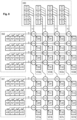
- FIGS. 2A to 2D illustrate the execution of variants of the read-scatter instruction on source matrices [a] and [b] of depth greater than 256 bits.
- the elements of the matrices are 16-bit words.
- a load instruction. 0 is executed.
- the memory address conveyed in the instruction designates, for example, the first element of the first row of matrix [a], namely the element a[0][0].
- the word WO returned on the bus therefore contains the elements a[0][0] to a[0][15].
- the instruction variant configures registers V0 to V3 to receive the respective four segments of the word WO in their first quarter.
- a load instruction. 1 is executed.
- the memory address designates the element a[1][0].
- the word W1 returned on the bus therefore contains the elements a[1][0] to a[1][15].
- the instruction variant configures registers V0 to V3 to receive the respective four segments of word W1 in their second quarter.
- a load instruction. 2 is executed.
- the memory address designates the element a[2][0].
- the word W2 returned on the bus therefore contains the elements a[2][0] to a[2][15].
- the instruction variant configures registers V0 to V3 to receive the respective four segments of word W2 in their third quarter.
- a load instruction. 3 is finally executed.
- the memory address designates the element a[3][0].
- the word W3 returned on the bus therefore contains the elements a[3][0] to a[3][15].
- the instruction variant configures registers V0 to V3 to receive the respective four segments of the word W3 in their fourth quarter.
- each of the registers V0 to V3 contains a consecutive sub-matrix [A] of 4x4 16-bit words (also denoted 4x4x16) in the direction of the rows of the source matrix [a].
- the rows of each submatrix are contained in four respective segments of the corresponding V register.
- Registers V0 to V3, containing sub-matrices [A], will be designated VA0 to VA3.
- each of these registers receives a consecutive submatrix [B] of 4x4x16 in the direction of the columns of the source matrix [b].
- the columns of each submatrix are contained in four respective segments of the corresponding VB register.
- VAi contains four vectors A[0] to A[3]
- VBj contains four vectors B[0] to B[3], each vector having four 16-bit components.
- FIG. 3 is a block diagram of an embodiment of a hardware calculation unit 16 of the coprocessor, intended to carry out a multiplication of two sub-matrices [A] and [B] in response to a single dedicated machine instruction that the we will note mm4a.
- This embodiment corresponds to the example considered in Figures 2A to 2B , where the matrix elements have a size of 16 bits.
- the calculation unit includes a matrix of 4x4 material operators of scalar product and accumulation denoted DP4A, where the number 4 designates the dimension of the vectors.
- a DP4A operator of row i and column j is wired to perform the scalar product of the vectors A[i] and B[j] contained respectively in registers VA and VB, and accumulate the scalar product in a cell Cij of a sub -result matrix [C].
- the cell Cij can be all or part of a segment of appropriate size of a register VC of the coprocessor.
- a comfortable size is 64 bits, which implies four registers VCa to VCd to store the result submatrix [C].
- the VA, VB and VC registers are designated by an mm4a instruction being executed in the central unit 10, here the VA0, VB0 and VC0a-VC0d registers.
- the VC registers are configured to preserve the Q-segment organization of the VA and VB registers.
- Q 4 and each result element is coded on 64 bits
- each of the 4 segments of the VC registers contains a single element.
- the VC registers are organized so that the four segments of the same register store elements of different rows.
- the contents of the four VC registers can be transferred to memory in four cycles to addresses corresponding to the positions of the columns of the sub-matrix [C] in the complete result matrix [c], thus contributing to a result matrix [c] stored by columns (“column-major”).
- the VC registers could also be organized in a complementary way so that the four segments of the same register store elements from different columns. In this case, the contents of the four VC registers can be transferred to memory in four cycles corresponding to the positions of the rows of the submatrix [C] in the complete result matrix [c], contributing to a result matrix [c] stored by rows (“row-major”).
- each of the registers VCa, VCb, VCc, VCd can be stored in memory to contribute to a row of the result matrix [c] stored by rows ("row-major").
- FIG 4 is a block diagram of a DP4A dot product operator of position (i, j) in the operator matrix.
- the operator processes vectors A[i] and B[j]. More specifically, the operator includes four 16-bit MUL multipliers each receiving a respective component (Ai0 to Ai3) of the vector A[i] as first multiplicand, and the corresponding component (B0j to B3j) of the vector B[j] as second multiplicand.
- the four products, coded on 32 bits, are supplied to a multi-adder 40 connected to accumulate the sum of the products in a 64-bit register segment Cij.
- By “accumulate” we mean that the Cij segment receives the sum of the products and previous content of the Cij segment.
- the multi-adder 40 is thus wired to perform the sum of four 32-bit numbers and one 64-bit number.
- the unit of calculation of Figure 3 wired in combinatorial logic, instantly produces the result matrix [C] in reaction to an mm4a instruction which designates the VA, VB and VC registers to use.
- a calculation unit taking into account the propagation delays of the combinatorial logic, will take more than one processor clock cycle to establish the result.
- the calculation unit in particular each DP4A operator, is generally designed in a pipeline structure, meaning that the calculation is broken down into several steps synchronized over successive clock cycles, but that a new calculation can be initiated, this is i.e. execute a new mm4a instruction, every clock cycle.
- a pipeline structure is not optimal for performing isolated calculations.
- the pipeline structure can be 100% efficient after an initial pipeline priming phase and before a final pipeline emptying phase.
- VLIW Very Large Instruction Word
- Table 1 below presents a sequence of instructions that allows you to multiply an 8x32 matrix [a] by a 32x8 matrix [b] to provide an 8x8 matrix [c] without downtime and using the full bandwidth of the memory bus and the parallel calculation unit. Instructions placed on the same line correspond to instructions executed in the same VLIW packet.
- the registers of the coprocessor are designated by Ax and By for the multiplicand sub-matrices and Cz for the result sub-matrix, knowing that all these registers, chosen from the set of registers 18 , are of the same nature.
- Phases 0 and 1 correspond to what we described in relation to the Figures 2A-2D .
- Phase 0 load the submatrices a[0..3] [0..3] to a[0..3] [12..15] load.0 A0A1A2A3 ⁇ - a[0] [0..15] load.1 A0A1A2A3 ⁇ - a[1] [0..15] load.2 A0A1A2A3 ⁇ - a[2] [0..15] load.3 A0A1A2A3 ⁇ - a[3] [0..15] Phase 1: load submatrices b[0..3] [0..3] to b[12..15] [0..3] load.0 80818283 ⁇ - b[0..15] [0] load.1 80818283 ⁇ - b[0..15] [1] load.2 80818283 ⁇ - b[0
- registers C0 to C15 contain the matrix result of the multiplication, an 8x8x64 matrix.
- phases 6 to 9 reuse the registers C of phases 2 to 5, namely the same result sub-matrices c[0..3][0..3], c[0..3][4. .7], c[4..7][0..3] and c[4..7][4..7].
- phases 2 to 5 we calculate the submatrices c[][] only on the first half of the depth of the source matrices (elements 0 to 15).
- phases 6 to 9 we update the sub-matrices c[][] with the influence of the second half of the depth of the source matrices (elements 16 to 31). This calculation naturally extends to any depth by updating the submatrices c[][] with the influence of the following 256-bit slices in the depth of the matrices [a] and [b].
- the source matrices mentioned as an example have a depth multiple of the width N of the memory bus.
- read-scatter operations affecting the last part of the rows (or columns) read words of which a first part contains the end of the row (or column), and the second part contains unusable data (either the start of a misaligned row or column, or arbitrary data after the end of the matrix).
- the data in the second part of the words are replaced by zeros, and the words thus readjusted are processed normally as explained previously.
- the depth of the matrices varies depending on the precision chosen for the elements.
- the elements can also be 8 or 32 bits without this affecting the organization of the source matrices in memory or their transfer to the coprocessor registers. Certain modifications can, however, be made in the calculation unit 16 of the coprocessor.
- FIG. 5 is a block diagram of an embodiment of a calculation unit 16 of the coprocessor, intended to carry out a multiplication of two sub-matrices [A] and [B] of 8-bit elements in response to a single instruction dedicated machine which will be noted mm8a.
- the dot product operators here denoted DP8A, are then configured to simultaneously calculate eight products and their sum.
- the precision of the results is 32 bits instead of 64 bits, which means that only two registers VC0a and VC0b are required to store the result submatrix [C].
- the VC registers are organized so that each segment stores two row elements of the result submatrix.
- register VC0a contains in its respective segments, the pairs (C00, C01), (C10, C11), (C20, C21) and (C30, C31).
- the contents of the two VC registers are not directly transferable to memory in the correct order to form a 4x4 submatrix of the result matrix [c].
- the processor's instruction set is extended by an instruction complementary to the read-disperse instruction, which we will designate by the gather-write or “gather-store” instruction.
- the execution of this instruction by the central processing unit configures the coprocessor to concatenate on the memory bus Q segments taken from Q designated registers.
- the position of the segment in the registers is defined by a corresponding variant of the instruction.
- the word WO contains the elements C00, C01 of the first segment of the register VC0a, followed by the elements C02, C03 of the first segment of the register VC0b, followed by the four elements of the first row of the second sub-matrix stored in the first segments of registers VC1a and VC1b (not shown).
- the remaining three cycles thus transfer the second to fourth rows of the two submatrices.
- the registers VD0a, VD0b, VD1a, VD1b can then be written in a conventional manner in a result matrix stored in rows while fully occupying the bandwidth of the bus.
- FIG. 6 is a block diagram of a DP8A dot product operator of position (i, j) in the operator matrix. It includes eight 8-bit multipliers each receiving a respective component (Ai0 to Ai7) of vector A[i] as first multiplicand, and the corresponding component (B0j to B7j) of vector B[j] as second multiplicand.
- the eight products, coded on 16 bits, are supplied to a multi-adder 40b connected to accumulate the sum of the products in a 32-bit register segment Cij.
- the transfer from memory to the coprocessor registers is always carried out in the same way, with a series of four read-scatter instructions.
- the register segments then contain vectors of two 32-bit elements.
- the dot product operators are then denoted DP2A and accumulate two products of 32-bit numbers in a 64- or 128-bit register segment.
- the matrix multiplication instruction is then denoted mm2a.
- FIG. 7 is a block diagram of a configurable dot product operator embodiment for processing matrix elements of adjustable precision among 8, 16, and 32 bits. It includes two 32-bit number multipliers, two 32-bit number multipliers, 16-bit numbers and four 8-bit number multipliers, the outputs of which are supplied to a multi-adder 40c, connected to accumulate the sum of the products in a 64- or 128-bit register segment Cij.
- the 32x32 multipliers are connected to process the first two components of the vectors, regardless of their precision.
- the only two components of a 2x32 bit vector are applied to all input lines of the 32x32 multipliers.
- Other multipliers produce a zero result.
- the 16x16 multipliers are connected to process the third and fourth components of 4x16 or 8x8 bit vectors.
- the first two components are applied respectively to the first 16 input lines of the two 32x32 multipliers, and the next two components are applied respectively to all the input lines of the two 16x16 multipliers.
- the first four components are applied respectively to the first 8 input lines of the two 32x32 multipliers and the two 16x16 multipliers, and the remaining components are applied respectively to all the input lines of the 8x8 multipliers.
- the organization of the connection of the multiplier inputs to the registers is determined by the nature of the executed matrix multiplication instruction, namely mm2a, mm4a or mm8a.
- the matrix elements can be integers or floating point numbers (in the latter case, the sizes 16 bits and 32 bits are used instead).
- Multipliers and adders are configured accordingly. If we want to deal with integers and floating point numbers, the multipliers will have a reconfigurable structure based on a floating point multiplication structure.
- the precision of the results could be 64 bits or 128 bits.
- a precision of 64 bits may be sufficient if we accept a certain level of error, in particular saturation when processing integers, or a rounding error when processing fixed or floating point numbers.
- registers A0-A3 are populated by a first series of four read-scatter instructions to contain four 4x4x16 submatrices taken from the first four rows of the source matrix [a]. In other words, these matrices contain rows a[0][0..15] to a[3][0..15].
- registers A4-A7 are populated by a second set of four read-scatter instructions to contain four 4x4x16 submatrices taken from the next four rows of matrix [a].
- these matrices contain rows a[4][0..15] to a[7][0..15].
- registers B0-B3 are populated by a third series of four read-scatter instructions to contain eight 4x4x8 submatrices taken from the first four columns of matrix [b].
- these matrices contain columns b[0..31][0] to b[0..31][3].
- the two halves of register B0 contain two submatrices, one of which b[0..3][0..3] can be multiplied with the submatrix a[0..3][0..3] of register A0 to contribute to the result submatrix c[0..3][0..3].
- the other submatrix b[4..7][0..3] of register B0 can be multiplied with the submatrix a[4..7][0..3] of register A4 to contribute to the result submatrix c[4..7][0..3].
- the two halves of register B1 contain two sub-matrices which can be multiplied respectively with the sub-matrices of registers A1 and A5 to contribute respectively to the same sub-matrices result c[0..3][0..3] and c[4..7][0..3].
- the two halves of register B2 respectively contain two sub-matrices to be multiplied with the sub-matrices of registers A2 and A6
- the two halves of register B3 respectively contain two sub-matrices to be multiplied with the sub-matrices of registers A3 and A7, each time to contribute to the same result submatrices c[0..3][0..3] and c[4..7][0..3], that is to say without changing the VC registers during these operations.
- both variants first configure the DP4A operators to use only the low 8 bits of the B inputs of the multipliers (called half inputs).
- the first variant further reconfigures the operators to connect the 16 8-bit half-entries to the first four bytes contained in each of the segments Bi0 to Bi3 of register B0.
- the second variant reconfigures the operators to connect the 16 8-bit half-entries to the last four bytes contained in each of the segments Bi0 to Bi3 of register B0.
- multiplicand matrix of 8-bit elements could thus have twice as many rows or columns as the corresponding multiplicand matrix of 16-bit elements.
- a calculation unit to multiply Q ⁇ Q ⁇ 16 submatrices by Qx(2Q)x8 submatrices, or vice versa (2Q)xQx8.
- the VB0 register is considered subdivided into two halves, each with 4 segments each containing a four-byte vector, and the DP4A dot product operators are organized into two 4x4 submatrices that simultaneously process the two respective halves of the VB0 register.
- a calculation unit comprising scalar product operators organized in a matrix RxQ with R > Q.
- Each register A then contains a submatrix of Q rows with elements of size N/Q bits
- each register B contains R/Q submatrices of Q columns with elements of size N/R bits, where N is the width of the memory bus and the size of the registers, and is divisible by Q and by R.
- Each multiplication instruction reads the contents of R/Q registers A and a register B, to produce a sub-matrix of dimensions RxQ.
Landscapes
- Engineering & Computer Science (AREA)
- Physics & Mathematics (AREA)
- Theoretical Computer Science (AREA)
- General Physics & Mathematics (AREA)
- Software Systems (AREA)
- General Engineering & Computer Science (AREA)
- Mathematical Physics (AREA)
- Mathematical Analysis (AREA)
- Mathematical Optimization (AREA)
- Pure & Applied Mathematics (AREA)
- Computational Mathematics (AREA)
- Data Mining & Analysis (AREA)
- Computing Systems (AREA)
- Algebra (AREA)
- Databases & Information Systems (AREA)
- Advance Control (AREA)
- Complex Calculations (AREA)
Claims (9)
- Verfahren zur Vervielfältigung von Matrizen, umfassend die Schritte:a) Speichern einer ersten Quellmatrix (a) in Reihen in einem gemeinsam genutzten Speicher, wobei aufeinanderfolgende Elemente einer Reihe der ersten Quellmatrix in aufeinanderfolgenden Speicheradressen gespeichert werden;b) Speichern einer zweiten Quellmatrix (b) in Spalten in dem gemeinsam genutzten Speicher, wobei aufeinanderfolgende Elemente einer Spalte der zweiten Quellmatrix in aufeinanderfolgenden Speicheradressen gespeichert werden;c) in einem einzigen Transferzyklus von dem gemeinsam genutzten Speicher zu Prozessorregistern (18) über einen Speicherbus aus N Bit:- Lesen eines Wortes aus N Bit in einer der ersten und zweiten Quellmatrizen;- Schreiben von K aufeinanderfolgenden Segmenten des Wortes aus N Bit an eine bezeichnete Position in K jeweiligen Registern (V) aus N Bit, wobei K so gewählt ist, dass N durch K teilbar ist;d) Durchführen von Schritt c) für K = R verschiedene Reihen der ersten Quellmatrix (a), um R erste Register (VA) zu füllen, wobei jedes der R ersten Register (VA0-VA3) eine verschiedene Untermatrix (A) von R Reihen von N/R Bit enthält, die in R aufeinanderfolgenden Segmenten (A0j-A3j) des Registers organisiert sind;e) Durchführen von Schritt c) für K = Q verschiedene Spalten der zweiten Quellmatrix (b), um Q zweite Register (VB) zu füllen, wobei jedes der Q zweiten Register (VB0-VB3) eine verschiedene Untermatrix (B) aus Q Spalten von N/Q Bit enthält, die in Q aufeinanderfolgenden Segmenten (Bi0-Bi3) des Registers organisiert sind; und(f) als Reaktion auf die Ausführung einer Maschinenanweisung zur Vervielfältigung von Untermatrizen, die als erste Operanden (VAO) eines der R ersten Register und als zweite Operanden (VBO) eines der Q zweiten Register bezeichnet werden, paralleles Durchführen, mit Hilfe eines dedizierten Hardware-Operators (DP4A), eines Skalarprodukts jedes Segments (A0j-A3j) des ersten Operandenregisters mit jedem Segment des zweiten Operandenregisters (Bi0-Bi3), wobei die Segmente der Operandenregister als Vektoren betrachtet werden.
- Verfahren nach Anspruch 1, umfassend die Schritte:- Empfangen in einer zentralen Verarbeitungseinheit eines Prozessors einer Maschinenanweisung zum Lesen und Streuen;- als Reaktion auf die Anweisung zum Lesen und Streuen Delegieren von Schritt c) an einen mit der zentralen Einheit gekoppelten Koprozessor, wobei die bezeichnete Position der K aufeinanderfolgenden Segmente und die Register durch die Anweisung zum Lesen und Streuen bestimmt werden;- Empfangen in der zentralen Einheit einer Maschinenanweisung zur Vervielfältigung von Untermatrizen; und- als Reaktion auf die Maschinenanweisung zur Vervielfältigung von Untermatrizen Delegieren von Schritt f) an den Koprozessor.
- Verfahren nach Anspruch 2, wobei die Verarbeitungseinheit und der Koprozessor gemäß einer VLIW-Architektur gekoppelt sind, wobei das Verfahren einen Schritt der gleichzeitigen Ausführung einer Anweisung zum Lesen und Streuen und einer Anweisung zur Vervielfältigung von Untermatrizen umfasst, die in demselben von der zentralen Einheit empfangenen Anweisungspaket enthalten sind, woraus sich ergibt, dass die Anweisung zum Lesen und Streuen eine nächste Operandenuntermatrix vorbereitet, während die Anweisung zur Vervielfältigung von Untermatrizen mit aktuellen Operandenuntermatrizen arbeitet.
- Verfahren nach Anspruch 1, wobei der Hardwareoperator ausgebildet ist, um jedes Skalarprodukt in einem jeweiligen Segment (Cij) eines Zielregisters (VC), das durch die Maschinenanweisung zur Vervielfältigung von Untermatrizen bestimmt wird, mit dem vorherigen Inhalt des jeweiligen Segments zu akkumulieren, wobei das Verfahren die Schritte umfasst:
Ausführen der Maschinenanweisung zur Vervielfältigung von Untermatrizen R-mal, wobei jedes Mal ein anderes Paar von gleichrangigen Operandenregistern (VAx, VBx) aus den R ersten Registern und den Q zweiten Registern und ein gleicher Satz von Zielregistern (VC0-VC3) bestimmt wird. - Verfahren nach Anspruch 1, wobei die Elemente jeder Quellmatrix eine konfigurierbare Genauigkeit von 8, 16 oder 32 Bit aufweisen.
- Prozessor, umfassend:- einen Datenbus aus N Bit, der für den Zugriff auf einen Speicher ausgebildet ist;- eine zentrale Verarbeitungseinheit (CPU), die mit dem Datenbus verbunden ist;- einen mit der zentralen Einheit gekoppelten Koprozessor, der Arbeitsregister (18) mit N Bit umfasst;- eine Anweisungsverarbeitungseinheit in der zentralen Einheit, die ausgebildet ist, um, als Reaktion auf eine von der Zentraleinheit empfangene Maschinenanweisung zum Lesen und Streuen, lesend auf eine Speicheradresse zuzugreifen und die Verarbeitung des entsprechenden Wortes (W) aus N Bit, das auf dem Datenbus ankommt, an den Koprozessor zu delegieren;- eine Registersteuereinheit im Koprozessor, die von der zentralen Einheit als Reaktion auf die Anweisung zum Lesen und Streuen ausgebildet ist, um das auf dem Datenbus ankommende Wort (W) in K Segmente zu unterteilen und die K Segmente an einer gleichen Position in K jeweilige Register (V0-V3) zu schreiben, wobei die Position und die Register durch die Maschinenanweisung zum Lesen und Streuen bestimmt werden.
- Prozessor nach Anspruch 6, der im Koprozessor eine Matrix von Hardwareoperatoren für das Skalarprodukt (DP4A) umfasst, wobei jeder Operator ausgebildet ist, um gleichzeitig das Skalarprodukt von zwei Vektoren (A0j-A3j, Bi0-Bi3) auszuführen, die in zwei Segmenten von zwei jeweiligen Operandenregistern (VAO, VBO) enthalten sind, wobei die Ränge der beiden Segmente in den Operandenregistern durch die Position des Operators in der Operatormatrix festgelegt sind und die Operandenregister durch eine von der zentralen Einheit empfangene Maschinenanweisung zur Vervielfältigung von Untermatrizen bestimmt werden, wodurch die Operandenregister jeweilige Operandenuntermatrizen enthalten und die Operatormatrix eine Ergebnisuntermatrix erzeugt.
- Prozessor nach Anspruch 7, wobei die Operatoren ausgebildet sind, um die Skalarprodukte in jeweiligen Segmenten von Zielregistern (VC) zu akkumulieren, die durch die Maschinenanweisung zur Vervielfältigung von Untermatrizen bestimmt werden.
- Prozessor nach Anspruch 7, wobei die Elemente jeder Operandenuntermatrix eine konfigurierbare Genauigkeit von 8, 16 oder 32 Bit aufweisen.
Applications Claiming Priority (1)
| Application Number | Priority Date | Filing Date | Title |
|---|---|---|---|
| FR1873594A FR3090932B1 (fr) | 2018-12-20 | 2018-12-20 | Système de multiplication de matrices par blocs |
Publications (3)
| Publication Number | Publication Date |
|---|---|
| EP3671488A1 EP3671488A1 (de) | 2020-06-24 |
| EP3671488C0 EP3671488C0 (de) | 2024-04-17 |
| EP3671488B1 true EP3671488B1 (de) | 2024-04-17 |
Family
ID=66641077
Family Applications (1)
| Application Number | Title | Priority Date | Filing Date |
|---|---|---|---|
| EP19214860.9A Active EP3671488B1 (de) | 2018-12-20 | 2019-12-10 | System zur blockweisen vervielfältigung von matrizen |
Country Status (4)
| Country | Link |
|---|---|
| US (1) | US11169808B2 (de) |
| EP (1) | EP3671488B1 (de) |
| CN (1) | CN111353126B (de) |
| FR (1) | FR3090932B1 (de) |
Families Citing this family (16)
| Publication number | Priority date | Publication date | Assignee | Title |
|---|---|---|---|---|
| US11169776B2 (en) * | 2019-06-28 | 2021-11-09 | Intel Corporation | Decomposed floating point multiplication |
| US11054998B1 (en) | 2019-12-12 | 2021-07-06 | Facebook, Inc. | High bandwidth memory system with distributed request broadcasting masters |
| CN113918879A (zh) * | 2020-07-08 | 2022-01-11 | 华为技术有限公司 | 矩阵运算的方法和加速器 |
| CN112506567B (zh) * | 2020-11-27 | 2022-11-04 | 海光信息技术股份有限公司 | 数据读取方法和数据读取电路 |
| CN112434256B (zh) * | 2020-12-03 | 2022-09-13 | 海光信息技术股份有限公司 | 矩阵乘法器和处理器 |
| CN112506468B (zh) * | 2020-12-09 | 2023-04-28 | 上海交通大学 | 支持高吞吐多精度乘法运算的risc-v通用处理器 |
| FR3118505B1 (fr) | 2020-12-31 | 2024-01-19 | Kalray | Système de traitement de matrices par plusieurs processeurs simultanément |
| US12002453B2 (en) * | 2021-03-25 | 2024-06-04 | Beijing Transtreams Technology Co. Ltd. | Methods and devices for irregular pruning for automatic speech recognition |
| CN114579929B (zh) * | 2022-03-14 | 2023-08-08 | 海飞科(南京)信息技术有限公司 | 加速器执行的方法和电子设备 |
| CN115114085B (zh) * | 2022-06-24 | 2025-08-05 | 山东云海国创云计算装备产业创新中心有限公司 | 一种数据恢复方法、装置、计算机设备及存储介质 |
| CN115373630B (zh) * | 2022-10-24 | 2022-12-20 | 北京麟卓信息科技有限公司 | 一种面向异构芯片的矩阵乘法运算过程优化方法 |
| CN116304513A (zh) * | 2023-03-16 | 2023-06-23 | 中国人民解放军国防科技大学 | 一种48位混合精度矩阵向量乘法实现方法及装置 |
| CN117093816B (zh) * | 2023-10-19 | 2024-01-19 | 上海登临科技有限公司 | 矩阵乘运算方法、装置和电子设备 |
| CN117454068B (zh) * | 2023-11-10 | 2025-01-24 | 上海壁仞科技股份有限公司 | 实现矩阵乘运算的方法和计算设备 |
| CN118227948B (zh) * | 2024-05-24 | 2024-08-06 | 北京壁仞科技开发有限公司 | 人工智能芯片、操作方法和机器可读存储介质 |
| CN120337997B (zh) * | 2025-06-17 | 2025-10-21 | 浪潮电子信息产业股份有限公司 | 基于人工智能模型的运行方法、装置、设备、介质和产品 |
Family Cites Families (14)
| Publication number | Priority date | Publication date | Assignee | Title |
|---|---|---|---|---|
| JP2556182B2 (ja) * | 1990-08-29 | 1996-11-20 | 三菱電機株式会社 | デ−タ処理装置 |
| US6170001B1 (en) * | 1998-05-27 | 2001-01-02 | Arm Limited | System for transfering format data from format register to memory wherein format data indicating the distribution of single or double precision data type in the register bank |
| US20040122887A1 (en) * | 2002-12-20 | 2004-06-24 | Macy William W. | Efficient multiplication of small matrices using SIMD registers |
| US20060179273A1 (en) * | 2005-02-09 | 2006-08-10 | Advanced Micro Devices, Inc. | Data processor adapted for efficient digital signal processing and method therefor |
| US7627735B2 (en) * | 2005-10-21 | 2009-12-01 | Intel Corporation | Implementing vector memory operations |
| EP2150889A1 (de) * | 2007-04-10 | 2010-02-10 | Cambridge Consultants Limited | Datenverarbeitungsvorrichtung |
| US8285766B2 (en) * | 2007-05-23 | 2012-10-09 | The Trustees Of Princeton University | Microprocessor shifter circuits utilizing butterfly and inverse butterfly routing circuits, and control circuits therefor |
| CN101609715B (zh) * | 2009-05-11 | 2012-09-05 | 中国人民解放军国防科学技术大学 | 行列访问端口分离的矩阵寄存器文件 |
| US9960917B2 (en) * | 2011-12-22 | 2018-05-01 | Intel Corporation | Matrix multiply accumulate instruction |
| US10055225B2 (en) * | 2011-12-23 | 2018-08-21 | Intel Corporation | Multi-register scatter instruction |
| CN103631761B (zh) * | 2012-08-29 | 2018-02-27 | 睿励科学仪器(上海)有限公司 | 并行处理架构进行矩阵运算并用于严格波耦合分析的方法 |
| US9384168B2 (en) * | 2013-06-11 | 2016-07-05 | Analog Devices Global | Vector matrix product accelerator for microprocessor integration |
| US9710279B2 (en) * | 2014-09-26 | 2017-07-18 | Intel Corporation | Method and apparatus for speculative vectorization |
| US9910827B2 (en) * | 2016-07-01 | 2018-03-06 | Hewlett Packard Enterprise Development Lp | Vector-matrix multiplications involving negative values |
-
2018
- 2018-12-20 FR FR1873594A patent/FR3090932B1/fr active Active
-
2019
- 2019-12-10 EP EP19214860.9A patent/EP3671488B1/de active Active
- 2019-12-20 US US16/724,106 patent/US11169808B2/en active Active
- 2019-12-20 CN CN201911323478.7A patent/CN111353126B/zh active Active
Also Published As
| Publication number | Publication date |
|---|---|
| US11169808B2 (en) | 2021-11-09 |
| US20200201642A1 (en) | 2020-06-25 |
| CN111353126B (zh) | 2025-02-18 |
| EP3671488C0 (de) | 2024-04-17 |
| CN111353126A (zh) | 2020-06-30 |
| FR3090932A1 (fr) | 2020-06-26 |
| EP3671488A1 (de) | 2020-06-24 |
| FR3090932B1 (fr) | 2022-05-27 |
Similar Documents
| Publication | Publication Date | Title |
|---|---|---|
| EP3671488B1 (de) | System zur blockweisen vervielfältigung von matrizen | |
| US11610100B2 (en) | Accelerator for deep neural networks | |
| US20240265234A1 (en) | Digital Processing Circuits and Methods of Matrix Operations in an Artificially Intelligent Environment | |
| EP3084588B1 (de) | Signalverarbeitungsmodul, insbesondere für neuronales netzwerk und neuronale schaltung | |
| EP0558125B1 (de) | Neuronaler Prozessor mit verteilten synaptischen Zellen | |
| BE897441A (fr) | Calculateur associatif permettant une multiplication rapide | |
| NL8304186A (nl) | Geintegreerde processor voor het verwerken van woordsgewijze ontvangbare informatie. | |
| EP4193358B1 (de) | Rekonfigurierbares speichermodul zur implementierung von rechenoperationen | |
| US11949414B2 (en) | Methods, apparatus, and articles of manufacture to improve in-memory multiply and accumulate operations | |
| US20220300253A1 (en) | Arithmetic operation device and arithmetic operation system | |
| EP0171305B1 (de) | Rechenschaltung für die diskrete Fouriertransformation | |
| FR2652174A1 (fr) | Dispositif pour manipuler des nombres dans un ordinateur. | |
| FR3118505A1 (fr) | Système de traitement de matrices par plusieurs processeurs simultanément | |
| FR3101980A1 (fr) | Processeur | |
| EP0397807A1 (de) | Vorrichtung zum gleichzeitigen filtrieren und wiederbemustern von rechnerdaten | |
| FR2652175A1 (fr) | Dispositif de conversion de nombres. | |
| US6307588B1 (en) | Method and apparatus for address expansion in a parallel image processing memory | |
| WO2000026790A1 (fr) | Memoire a acces vectoriel | |
| WO2025156728A1 (zh) | 数据处理方法、处理阵列及处理装置 | |
| EP0291613A1 (de) | Prozessor mit einer Mehrheit von seriell geschalteten Stufen | |
| EP0254628B1 (de) | Digitale Signalverarbeitungseinrichtung zur Ausführung einer Kosinustransformation | |
| EP4672013A1 (de) | Automatisches datenroutingmodul für rechner mit simd-architektur | |
| WO2024197292A2 (en) | Apparatus and method for compute in bram for multiply-accumulate operations | |
| FR2611286A1 (fr) | Circuit integre multiplieur, et son procede de composition | |
| FR2629930A1 (fr) | Procede et unite de gestion de mots d'adresse |
Legal Events
| Date | Code | Title | Description |
|---|---|---|---|
| PUAI | Public reference made under article 153(3) epc to a published international application that has entered the european phase |
Free format text: ORIGINAL CODE: 0009012 |
|
| STAA | Information on the status of an ep patent application or granted ep patent |
Free format text: STATUS: THE APPLICATION HAS BEEN PUBLISHED |
|
| AK | Designated contracting states |
Kind code of ref document: A1 Designated state(s): AL AT BE BG CH CY CZ DE DK EE ES FI FR GB GR HR HU IE IS IT LI LT LU LV MC MK MT NL NO PL PT RO RS SE SI SK SM TR |
|
| AX | Request for extension of the european patent |
Extension state: BA ME |
|
| STAA | Information on the status of an ep patent application or granted ep patent |
Free format text: STATUS: REQUEST FOR EXAMINATION WAS MADE |
|
| 17P | Request for examination filed |
Effective date: 20201211 |
|
| RBV | Designated contracting states (corrected) |
Designated state(s): AL AT BE BG CH CY CZ DE DK EE ES FI FR GB GR HR HU IE IS IT LI LT LU LV MC MK MT NL NO PL PT RO RS SE SI SK SM TR |
|
| REG | Reference to a national code |
Ref country code: DE Ref legal event code: R079 Free format text: PREVIOUS MAIN CLASS: G06F0017160000 Ref document number: 602019050367 Country of ref document: DE Ipc: G06F0012060000 |
|
| GRAP | Despatch of communication of intention to grant a patent |
Free format text: ORIGINAL CODE: EPIDOSNIGR1 |
|
| STAA | Information on the status of an ep patent application or granted ep patent |
Free format text: STATUS: GRANT OF PATENT IS INTENDED |
|
| RIC1 | Information provided on ipc code assigned before grant |
Ipc: G06F 17/16 20060101ALI20231130BHEP Ipc: G06F 12/06 20060101AFI20231130BHEP |
|
| INTG | Intention to grant announced |
Effective date: 20231222 |
|
| GRAS | Grant fee paid |
Free format text: ORIGINAL CODE: EPIDOSNIGR3 |
|
| GRAA | (expected) grant |
Free format text: ORIGINAL CODE: 0009210 |
|
| STAA | Information on the status of an ep patent application or granted ep patent |
Free format text: STATUS: THE PATENT HAS BEEN GRANTED |
|
| AK | Designated contracting states |
Kind code of ref document: B1 Designated state(s): AL AT BE BG CH CY CZ DE DK EE ES FI FR GB GR HR HU IE IS IT LI LT LU LV MC MK MT NL NO PL PT RO RS SE SI SK SM TR |
|
| REG | Reference to a national code |
Ref country code: GB Ref legal event code: FG4D Free format text: NOT ENGLISH |
|
| REG | Reference to a national code |
Ref country code: CH Ref legal event code: EP |
|
| REG | Reference to a national code |
Ref country code: DE Ref legal event code: R096 Ref document number: 602019050367 Country of ref document: DE |
|
| REG | Reference to a national code |
Ref country code: IE Ref legal event code: FG4D Free format text: LANGUAGE OF EP DOCUMENT: FRENCH |
|
| U01 | Request for unitary effect filed |
Effective date: 20240507 |
|
| U07 | Unitary effect registered |
Designated state(s): AT BE BG DE DK EE FI FR IT LT LU LV MT NL PT SE SI Effective date: 20240521 |
|
| PG25 | Lapsed in a contracting state [announced via postgrant information from national office to epo] |
Ref country code: IS Free format text: LAPSE BECAUSE OF FAILURE TO SUBMIT A TRANSLATION OF THE DESCRIPTION OR TO PAY THE FEE WITHIN THE PRESCRIBED TIME-LIMIT Effective date: 20240817 |
|
| PG25 | Lapsed in a contracting state [announced via postgrant information from national office to epo] |
Ref country code: HR Free format text: LAPSE BECAUSE OF FAILURE TO SUBMIT A TRANSLATION OF THE DESCRIPTION OR TO PAY THE FEE WITHIN THE PRESCRIBED TIME-LIMIT Effective date: 20240417 |
|
| PG25 | Lapsed in a contracting state [announced via postgrant information from national office to epo] |
Ref country code: GR Free format text: LAPSE BECAUSE OF FAILURE TO SUBMIT A TRANSLATION OF THE DESCRIPTION OR TO PAY THE FEE WITHIN THE PRESCRIBED TIME-LIMIT Effective date: 20240718 |
|
| PG25 | Lapsed in a contracting state [announced via postgrant information from national office to epo] |
Ref country code: ES Free format text: LAPSE BECAUSE OF FAILURE TO SUBMIT A TRANSLATION OF THE DESCRIPTION OR TO PAY THE FEE WITHIN THE PRESCRIBED TIME-LIMIT Effective date: 20240417 |
|
| PG25 | Lapsed in a contracting state [announced via postgrant information from national office to epo] |
Ref country code: PL Free format text: LAPSE BECAUSE OF FAILURE TO SUBMIT A TRANSLATION OF THE DESCRIPTION OR TO PAY THE FEE WITHIN THE PRESCRIBED TIME-LIMIT Effective date: 20240417 |
|
| PG25 | Lapsed in a contracting state [announced via postgrant information from national office to epo] |
Ref country code: PL Free format text: LAPSE BECAUSE OF FAILURE TO SUBMIT A TRANSLATION OF THE DESCRIPTION OR TO PAY THE FEE WITHIN THE PRESCRIBED TIME-LIMIT Effective date: 20240417 Ref country code: NO Free format text: LAPSE BECAUSE OF FAILURE TO SUBMIT A TRANSLATION OF THE DESCRIPTION OR TO PAY THE FEE WITHIN THE PRESCRIBED TIME-LIMIT Effective date: 20240717 Ref country code: IS Free format text: LAPSE BECAUSE OF FAILURE TO SUBMIT A TRANSLATION OF THE DESCRIPTION OR TO PAY THE FEE WITHIN THE PRESCRIBED TIME-LIMIT Effective date: 20240817 Ref country code: HR Free format text: LAPSE BECAUSE OF FAILURE TO SUBMIT A TRANSLATION OF THE DESCRIPTION OR TO PAY THE FEE WITHIN THE PRESCRIBED TIME-LIMIT Effective date: 20240417 Ref country code: GR Free format text: LAPSE BECAUSE OF FAILURE TO SUBMIT A TRANSLATION OF THE DESCRIPTION OR TO PAY THE FEE WITHIN THE PRESCRIBED TIME-LIMIT Effective date: 20240718 Ref country code: ES Free format text: LAPSE BECAUSE OF FAILURE TO SUBMIT A TRANSLATION OF THE DESCRIPTION OR TO PAY THE FEE WITHIN THE PRESCRIBED TIME-LIMIT Effective date: 20240417 Ref country code: RS Free format text: LAPSE BECAUSE OF FAILURE TO SUBMIT A TRANSLATION OF THE DESCRIPTION OR TO PAY THE FEE WITHIN THE PRESCRIBED TIME-LIMIT Effective date: 20240717 |
|
| REG | Reference to a national code |
Ref country code: DE Ref legal event code: R097 Ref document number: 602019050367 Country of ref document: DE |
|
| U20 | Renewal fee for the european patent with unitary effect paid |
Year of fee payment: 6 Effective date: 20241216 |
|
| PG25 | Lapsed in a contracting state [announced via postgrant information from national office to epo] |
Ref country code: CZ Free format text: LAPSE BECAUSE OF FAILURE TO SUBMIT A TRANSLATION OF THE DESCRIPTION OR TO PAY THE FEE WITHIN THE PRESCRIBED TIME-LIMIT Effective date: 20240417 |
|
| PG25 | Lapsed in a contracting state [announced via postgrant information from national office to epo] |
Ref country code: SK Free format text: LAPSE BECAUSE OF FAILURE TO SUBMIT A TRANSLATION OF THE DESCRIPTION OR TO PAY THE FEE WITHIN THE PRESCRIBED TIME-LIMIT Effective date: 20240417 Ref country code: RO Free format text: LAPSE BECAUSE OF FAILURE TO SUBMIT A TRANSLATION OF THE DESCRIPTION OR TO PAY THE FEE WITHIN THE PRESCRIBED TIME-LIMIT Effective date: 20240417 |
|
| PG25 | Lapsed in a contracting state [announced via postgrant information from national office to epo] |
Ref country code: SM Free format text: LAPSE BECAUSE OF FAILURE TO SUBMIT A TRANSLATION OF THE DESCRIPTION OR TO PAY THE FEE WITHIN THE PRESCRIBED TIME-LIMIT Effective date: 20240417 |
|
| PG25 | Lapsed in a contracting state [announced via postgrant information from national office to epo] |
Ref country code: SM Free format text: LAPSE BECAUSE OF FAILURE TO SUBMIT A TRANSLATION OF THE DESCRIPTION OR TO PAY THE FEE WITHIN THE PRESCRIBED TIME-LIMIT Effective date: 20240417 Ref country code: SK Free format text: LAPSE BECAUSE OF FAILURE TO SUBMIT A TRANSLATION OF THE DESCRIPTION OR TO PAY THE FEE WITHIN THE PRESCRIBED TIME-LIMIT Effective date: 20240417 Ref country code: RO Free format text: LAPSE BECAUSE OF FAILURE TO SUBMIT A TRANSLATION OF THE DESCRIPTION OR TO PAY THE FEE WITHIN THE PRESCRIBED TIME-LIMIT Effective date: 20240417 Ref country code: CZ Free format text: LAPSE BECAUSE OF FAILURE TO SUBMIT A TRANSLATION OF THE DESCRIPTION OR TO PAY THE FEE WITHIN THE PRESCRIBED TIME-LIMIT Effective date: 20240417 |
|
| PLBE | No opposition filed within time limit |
Free format text: ORIGINAL CODE: 0009261 |
|
| STAA | Information on the status of an ep patent application or granted ep patent |
Free format text: STATUS: NO OPPOSITION FILED WITHIN TIME LIMIT |
|
| 26N | No opposition filed |
Effective date: 20250120 |
|
| PG25 | Lapsed in a contracting state [announced via postgrant information from national office to epo] |
Ref country code: MC Free format text: LAPSE BECAUSE OF FAILURE TO SUBMIT A TRANSLATION OF THE DESCRIPTION OR TO PAY THE FEE WITHIN THE PRESCRIBED TIME-LIMIT Effective date: 20240417 |
|
| PG25 | Lapsed in a contracting state [announced via postgrant information from national office to epo] |
Ref country code: IE Free format text: LAPSE BECAUSE OF NON-PAYMENT OF DUE FEES Effective date: 20241210 |
|
| REG | Reference to a national code |
Ref country code: CH Ref legal event code: U11 Free format text: ST27 STATUS EVENT CODE: U-0-0-U10-U11 (AS PROVIDED BY THE NATIONAL OFFICE) Effective date: 20260108 |
|
| PGFP | Annual fee paid to national office [announced via postgrant information from national office to epo] |
Ref country code: GB Payment date: 20251229 Year of fee payment: 7 |
|
| U20 | Renewal fee for the european patent with unitary effect paid |
Year of fee payment: 7 Effective date: 20251215 |
|
| PGFP | Annual fee paid to national office [announced via postgrant information from national office to epo] |
Ref country code: CH Payment date: 20260108 Year of fee payment: 7 |