EP3671561A1 - Herstellungsverfahren einer metallischen funkfrequenz-chipkarte mit verbesserter elektromagnetischer leitfähigkeit - Google Patents
Herstellungsverfahren einer metallischen funkfrequenz-chipkarte mit verbesserter elektromagnetischer leitfähigkeit Download PDFInfo
- Publication number
- EP3671561A1 EP3671561A1 EP18306803.0A EP18306803A EP3671561A1 EP 3671561 A1 EP3671561 A1 EP 3671561A1 EP 18306803 A EP18306803 A EP 18306803A EP 3671561 A1 EP3671561 A1 EP 3671561A1
- Authority
- EP
- European Patent Office
- Prior art keywords
- plate
- antenna
- slots
- radio frequency
- insert
- Prior art date
- Legal status (The legal status is an assumption and is not a legal conclusion. Google has not performed a legal analysis and makes no representation as to the accuracy of the status listed.)
- Withdrawn
Links
Images

Classifications
-
- G—PHYSICS
- G06—COMPUTING OR CALCULATING; COUNTING
- G06K—GRAPHICAL DATA READING; PRESENTATION OF DATA; RECORD CARRIERS; HANDLING RECORD CARRIERS
- G06K19/00—Record carriers for use with machines and with at least a part designed to carry digital markings
- G06K19/02—Record carriers for use with machines and with at least a part designed to carry digital markings characterised by the selection of materials, e.g. to avoid wear during transport through the machine
-
- G—PHYSICS
- G06—COMPUTING OR CALCULATING; COUNTING
- G06K—GRAPHICAL DATA READING; PRESENTATION OF DATA; RECORD CARRIERS; HANDLING RECORD CARRIERS
- G06K19/00—Record carriers for use with machines and with at least a part designed to carry digital markings
- G06K19/06—Record carriers for use with machines and with at least a part designed to carry digital markings characterised by the kind of the digital marking, e.g. shape, nature, code
- G06K19/067—Record carriers with conductive marks, printed circuits or semiconductor circuit elements, e.g. credit or identity cards also with resonating or responding marks without active components
- G06K19/07—Record carriers with conductive marks, printed circuits or semiconductor circuit elements, e.g. credit or identity cards also with resonating or responding marks without active components with integrated circuit chips
- G06K19/077—Constructional details, e.g. mounting of circuits in the carrier
- G06K19/0772—Physical layout of the record carrier
-
- G—PHYSICS
- G06—COMPUTING OR CALCULATING; COUNTING
- G06K—GRAPHICAL DATA READING; PRESENTATION OF DATA; RECORD CARRIERS; HANDLING RECORD CARRIERS
- G06K19/00—Record carriers for use with machines and with at least a part designed to carry digital markings
- G06K19/06—Record carriers for use with machines and with at least a part designed to carry digital markings characterised by the kind of the digital marking, e.g. shape, nature, code
- G06K19/067—Record carriers with conductive marks, printed circuits or semiconductor circuit elements, e.g. credit or identity cards also with resonating or responding marks without active components
- G06K19/07—Record carriers with conductive marks, printed circuits or semiconductor circuit elements, e.g. credit or identity cards also with resonating or responding marks without active components with integrated circuit chips
- G06K19/077—Constructional details, e.g. mounting of circuits in the carrier
- G06K19/07749—Constructional details, e.g. mounting of circuits in the carrier the record carrier being capable of non-contact communication, e.g. constructional details of the antenna of a non-contact smart card
- G06K19/07771—Constructional details, e.g. mounting of circuits in the carrier the record carrier being capable of non-contact communication, e.g. constructional details of the antenna of a non-contact smart card the record carrier comprising means for minimising adverse effects on the data communication capability of the record carrier, e.g. minimising Eddy currents induced in a proximate metal or otherwise electromagnetically interfering object
-
- G—PHYSICS
- G06—COMPUTING OR CALCULATING; COUNTING
- G06K—GRAPHICAL DATA READING; PRESENTATION OF DATA; RECORD CARRIERS; HANDLING RECORD CARRIERS
- G06K19/00—Record carriers for use with machines and with at least a part designed to carry digital markings
- G06K19/06—Record carriers for use with machines and with at least a part designed to carry digital markings characterised by the kind of the digital marking, e.g. shape, nature, code
- G06K19/067—Record carriers with conductive marks, printed circuits or semiconductor circuit elements, e.g. credit or identity cards also with resonating or responding marks without active components
- G06K19/07—Record carriers with conductive marks, printed circuits or semiconductor circuit elements, e.g. credit or identity cards also with resonating or responding marks without active components with integrated circuit chips
- G06K19/077—Constructional details, e.g. mounting of circuits in the carrier
- G06K19/07749—Constructional details, e.g. mounting of circuits in the carrier the record carrier being capable of non-contact communication, e.g. constructional details of the antenna of a non-contact smart card
- G06K19/07773—Antenna details
Definitions
- the invention relates to the field of contactless smart cards comprising a high metallic content or a metal plate extending to at least one edge of the card and a radio frequency integrated circuit chip module.
- It relates in particular to the manufacture of a smart card comprising at least one metal plate in the card body and having improved electromagnetic permittivity.
- Smart cards can be of the hybrid type (contacts and contactless) or purely contactless (without electrical contact terminal block).
- the plate is in principle included in an insert covered by at least one sheet or external covering film.
- Smart cards can have a smart card module comprising a radiofrequency transponder with the chip and the antenna carried on an insulating substrate of the module.
- the radio frequency chip card modules are generally inserted in a cavity of the card body. They can also connect an antenna housed in the card body via electrical interconnection elements, connecting terminal areas of the antenna to connection areas of the chip placed on the module.
- a smart card radio frequency module can be coupled with a passive antenna or relay housed in the card body.
- the invention relates more particularly to metallic bank, payment and transport cards.
- the patent FR 2743649 describes a smart card module with antenna and / or contact pads which can be incorporated into a card body cavity or which can form an RFID electronic tag.
- hybrid radio frequency devices such as contact and contactless cards, comprising a smart card module with contacts incorporated in a card body and connected to an antenna housed in the card body.
- bank cards comprising metal elements in the insert inside the plastic card body or on the external surface of the card body such as aluminum, titanium, gold.
- the metal provides a feeling of heaviness of the card which is very appreciated by the users. It also gives a visible aesthetic appearance which makes it a high-end product for the privileged.
- the patent application US2015 / 0269477 A1 describes a metal chip card comprising an antenna on a substrate and a metal plate with a series of holes, arranged on the substrate. The holes are arranged above the path of the antenna turns.
- the radio frequency communications performance tested by the inventors is insufficient despite the presence of holes above the path of the antenna turns.
- the invention aims to solve the aforementioned drawbacks.
- the invention relates to a metal card structure which includes better communication performance than in the prior art.
- the card can preferably also have a structure satisfying the constraints of mechanical strength - in terms of ISO for all the other tests and of durability over time.
- the invention consists, according to a preferred aspect, in a particular arrangement (or configuration) of the perforations or recesses in a metal plate so as to increase the permittivity of the metal plate with regard to an electromagnetic field of a radio frequency reader.
- the holes are elongated and arranged along the path of antenna turns and metal-free passages extend from each slot to the edge of the plate to open there.
- This configuration of the perforations allows a good distribution of the radiofrequency field in the card despite the presence of metal and which leads to good communication performance both in the two directions of the Z axis perpendicular to the main plane X, Y of the card but also laterally in this plane.
- the method is characterized in that said perforations comprise at least two slots each extending along and facing a portion of antenna turns, each slot also opening onto the edge of the plate via a passage formed on said edge .
- the subject of the invention is also a metal insert for a radio frequency chip card, said insert comprising an assembly of an insulating substrate with a metal plate, said substrate carrying at least one antenna turn and said plate comprising radiofrequency permittivity perforations and a receiving cavity of a radio frequency chip module, said perforations being arranged opposite said antenna turn, characterized in that said perforations comprise at least two slots each extending along opposite or parallel edges of said plate, along and facing a portion of antenna coil, each slot also opening onto the edge of the plate via a passage formed on said edge.
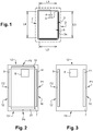
- the method provides for the formation or the supply of an assembly 1 ( figure 4 ) comprising an insulating substrate 2 visible on the Figures 1 and 3 and a metal plate visible on the figure 2 .
- the substrate 2 carries at least one antenna turn 3 with two terminal ends 4, 5, resting on said substrate, and a coupling surface 6 inside the outer turn 3 of the antenna 3;
- the antenna in smart card format can be produced at the same time as a plurality of antennas on a large-format insulating substrate (example 60 x 100 cm), in particular of plastic material such as PVC, PC, PET.
- the antenna can be extracted later at the dotted line "D" which can illustrate the periphery of the insert, by punching or laser cutting while being associated or not with a metal plate.
- the antenna is produced here by incrustation of wire by ultrasound but can be carried out by any known technique such as the etching of copper, aluminum, serigraphy, a deposit of jet of conductive material, a cutting of antenna by punching or laser in a metal sheet.
- the antenna may have its terminal ends 4, 5 for interconnection to a module also preferably resting on the substrate 3 without being an obligation. Its ends may remain in the air.
- the terminal ends are also produced by zigzags of inlaid wires. They can be produced by any known technique relating to the above antenna.
- the ends can constitute or include or be replaced by a coupling and / or interconnection interface such as for example a coupling coil to connect a radio frequency transponder in an antenna module.
- the assembly 1 also comprises, as indicated above, a metal plate 7 ( fig. 2 or fig. 3 ) comprising perforations 9, 11, 19, 21 of radio frequency permittivity, a cavity 8 for receiving a radio frequency chip module.
- the perforations and the cavity pass right through the plate.
- the perforations 9 and 11 are arranged respectively opposite said antenna turn and its ends.
- the perforations comprise at least two longitudinal slots 9, 11 each extending on at least one of the edges (10, 12) (preferably diametrically or symmetrically) of said plate 7, along and opposite a portion L3, L4 of antenna turn (3), each slot 9, 11 also opening onto the edge 10, 12 of the plate via a passage P1, P2 formed on said edge 10, 12.
- the passage P1, P2 can be located anywhere on the side or the edge of the card. In the examples, the passages are located substantially in the center of each slot or elongated opening 9, 11. However, each passage can be positioned substantially in a central area or start area or end area of each slot.
- the passages may have, for example a width of approximately 0.5 to 5 mm.
- the portions of turns L1 and L2 have substantially the width of a smart card body.
- the slots 9 and 11 have substantially the same lengths as these portions of antenna turns.
- turns L1 and L2 are here symmetrically opposite since the slots cover the transverse sides of the antenna 3 of rectangular shape extending along the peripheral edges of the chip card insert or of assembly 1. These portions of turns (here rectilinear) are separated from an intermediate central zone 6 forming an electromagnetic coupling surface inside the external turn 3e of the antenna in the form of a spiral or coil.
- portions L1 and L2 of turns can be replaced respectively by longitudinal portions L3 and L4.
- the lengths L1, L2, L3, L4 can be between 3 cm and 5 cm.
- L1-L4 openings or perforations are made over the width of the card, we could have a length of between 2.5 cm to 4.9 cm. If we make openings or perforations L1-L4 along the length we could have between 4.5 cm 8.2 cm.
- the slots 9 and 11 may extend over almost the entire width or length of the metal plate and be just set back a few millimeters 4 to 15 mm from the longitudinal peripheral edges.
- the slots here have a width "La" of 5 to 6 mm to reveal 6 antenna turns. More precisely, the width of the openings or slots may preferably be greater than the width of the bundle of turns by at least 1 mm on either side of the bundle.
- the metal plate here is a steel plate with a thickness equal to approximately 500 ⁇ m. It can vary from 150 to 650 ⁇ m. It can be composed of an assembly of several metal plates.
- the antenna has a non-rectangular, oval or rounded shape and the targeted portions of turns can be diametrically opposite.
- the turns portions extend in the immediate vicinity of lateral or longitudinal edges of the plate.
- the turns can for example be set back 2 to 5 mm from these edges so as to have the maximum coupling surface inside the external turn.
- the method according to the preferred mode may comprise the formation in said plate, of at least four slots 9, 11, 19, 21, each of said slots extending respectively on at least one of the four sides of said plate , along and facing a significant portion of the antenna turn, each slot opening out via a passage, also on one of the external edges of said plate adjacent or parallel to said slot.
- the elongated slots form an electro-magnetically more permeable and more efficient passage than a series of holes of the prior art offering comparatively the same surface of removed metal.
- the passages P1-P4 can be filled with resin at a later date, in particular during assembly with sheets of covers.
- a simply radio frequency module M1 can be connected to the antenna before being assembled to the plate of the figure 2 or that of the figure 3 .
- a M2 smart card module (contacts and contactless) can in particular be connected after laminating sheets and machining a cavity.
- the module can be connected to the terminal portions 4, 5 of interconnection of the antenna 3.
- the module can be connected capacitively for example by having at least one capacitor plate opposite the one of tracks 4 or 5.
- the module can also be connected inductively with the antenna which can be configured to form a passive or relay antenna.
- the cavity may in a known manner comprise a small coil (not shown) at the levels 4 and 5 in order to form an electromagnetic coupling loop which couples with an antenna module and radio frequency chip introduced above the coil of coupling.
- the radio frequency chip of the module can be connected in an ohmic or capacitive or inductive manner to said antenna 3.
- the assembly or insert 1 can then be covered with at least one or more sheets or polymer layers of cover or decoration. It can then be cut with standard smart card format with metallic card edges.
- the method can provide for placing metal plates of a format slightly smaller than the format of a smart card on each substrate 3 and laminating sheets of covers by the after.
- the slots Prior to the addition of cover sheets, the slots (or even the cavity 8) are preferably filled with polymer resin.
- the cavity 8 can be subsequently updated again with the interconnection pads 4, and 5 after the laminating of the cover sheets.
- the invention provides a metal insert structure for a radio frequency chip card comprising the characteristics below and which can be obtained in particular by the steps of the method illustrated in figure 6 .
- the insert can generally comprise an assembly 1 ( figure 4 ) of an insulating substrate 2 with a metal plate 7.
- the substrate carries at least one antenna turn 3 and the plate 7 comprises radiofrequency permittivity perforations and a cavity 8 for receiving a radiofrequency chip module.
- the cavity can be carried out at the same time as the slots or later after having covered the assembly with at least one or more cover sheets on at least one of the main faces.
- the perforations are arranged opposite the antenna coil 3.
- the perforations comprise at least two longitudinal slots 9, 11, (or even four preferably) each extending, preferably, over at least one of the edges 10, 12 (symmetrically or diametrically) opposite of said plate 7, along and facing a portion L3, L4 of antenna turn 3, each slot 9, 11 also opening onto the edge 10, 12 of the plate via a passage (or a gap P1, P2) formed on said edge 10, 12.
- the assembly may include ferrite rods inserted into the slots (and facing the module cavity) to improve the passage of electromagnetic flux at least in a direction substantially perpendicular to a main plane of the card and to weigh down even more the metal plate. Ferrite rods at least improve communication to one side of the card.
- the smart card according to the invention can use a hybrid radio frequency smart module comprising contact pads which can also be perforated, outside the reserved areas of standardized contact in order to further improve the electromagnetic permittivity.
- the method can provide in each embodiment to make thinning 14-20 of the plate at places situated opposite the antenna turns 3. This in order to avoid excess thicknesses.
- the card body plate can comprise an assembly of metal plates welded together or assembled by means of a thin adhesive layer. This last assembly can improve the mechanical resistance of bending / torsion.
- the invention allows easy fabrication of a smart card comprising the insert described above for radio frequency performance compatible with smart card standards, in particular EMVco.
Landscapes
- Engineering & Computer Science (AREA)
- Physics & Mathematics (AREA)
- General Physics & Mathematics (AREA)
- Theoretical Computer Science (AREA)
- Computer Hardware Design (AREA)
- Microelectronics & Electronic Packaging (AREA)
- Computer Networks & Wireless Communication (AREA)
- Electromagnetism (AREA)
- Credit Cards Or The Like (AREA)
- Details Of Aerials (AREA)
- Waveguide Aerials (AREA)
Priority Applications (5)
| Application Number | Priority Date | Filing Date | Title |
|---|---|---|---|
| EP18306803.0A EP3671561A1 (de) | 2018-12-21 | 2018-12-21 | Herstellungsverfahren einer metallischen funkfrequenz-chipkarte mit verbesserter elektromagnetischer leitfähigkeit |
| CN201990001252.2U CN216561809U (zh) | 2018-12-21 | 2019-12-06 | 具有改进的电磁介电常数的金属射频芯片卡和金属嵌体 |
| EP19813060.1A EP3899792B1 (de) | 2018-12-21 | 2019-12-06 | Herstellungsverfahren einer metallischen funkfrequenz-chipkarte mit verbesserter elektromagnetischer leitfähigkeit |
| PCT/EP2019/084085 WO2020126571A1 (fr) | 2018-12-21 | 2019-12-06 | Procede de fabrication d'une carte a puce radiofrequence metallique a permittivite electromagnetique amelioree |
| US17/416,862 US11501127B2 (en) | 2018-12-21 | 2019-12-06 | Method for producing a metal radio-frequency chip card with improved electromagnetic permittivity |
Applications Claiming Priority (1)
| Application Number | Priority Date | Filing Date | Title |
|---|---|---|---|
| EP18306803.0A EP3671561A1 (de) | 2018-12-21 | 2018-12-21 | Herstellungsverfahren einer metallischen funkfrequenz-chipkarte mit verbesserter elektromagnetischer leitfähigkeit |
Publications (1)
| Publication Number | Publication Date |
|---|---|
| EP3671561A1 true EP3671561A1 (de) | 2020-06-24 |
Family
ID=65200527
Family Applications (2)
| Application Number | Title | Priority Date | Filing Date |
|---|---|---|---|
| EP18306803.0A Withdrawn EP3671561A1 (de) | 2018-12-21 | 2018-12-21 | Herstellungsverfahren einer metallischen funkfrequenz-chipkarte mit verbesserter elektromagnetischer leitfähigkeit |
| EP19813060.1A Active EP3899792B1 (de) | 2018-12-21 | 2019-12-06 | Herstellungsverfahren einer metallischen funkfrequenz-chipkarte mit verbesserter elektromagnetischer leitfähigkeit |
Family Applications After (1)
| Application Number | Title | Priority Date | Filing Date |
|---|---|---|---|
| EP19813060.1A Active EP3899792B1 (de) | 2018-12-21 | 2019-12-06 | Herstellungsverfahren einer metallischen funkfrequenz-chipkarte mit verbesserter elektromagnetischer leitfähigkeit |
Country Status (4)
| Country | Link |
|---|---|
| US (1) | US11501127B2 (de) |
| EP (2) | EP3671561A1 (de) |
| CN (1) | CN216561809U (de) |
| WO (1) | WO2020126571A1 (de) |
Families Citing this family (2)
| Publication number | Priority date | Publication date | Assignee | Title |
|---|---|---|---|---|
| WO2023034642A1 (en) | 2021-09-06 | 2023-03-09 | Metaland Llc | Encapsulating a metal inlay with thermosetting resin and method for making a metal transaction card |
| US12159180B1 (en) | 2021-11-29 | 2024-12-03 | Metaland Llc | RFID enabled metal transaction cards with coupler coil couplings and related methods |
Citations (5)
| Publication number | Priority date | Publication date | Assignee | Title |
|---|---|---|---|---|
| FR2743649A1 (fr) | 1996-01-17 | 1997-07-18 | Gemplus Card Int | Module electronique sans contact, carte etiquette electronique l'incorporant, et leurs procedes de fabrication |
| EP2612764A2 (de) * | 2010-09-01 | 2013-07-10 | Hyundai Card Co., Ltd. | Metallzahlkarte und verfahren zu ihrer herstellung |
| US20150269477A1 (en) | 2012-08-30 | 2015-09-24 | David Finn | Dual-interface hybrid metal smartcard with a booster antenna or coupling frame |
| US20180132376A1 (en) * | 2015-04-02 | 2018-05-10 | Amogreentech Co., Ltd. | Heat Dissipation Unit For Wireless Charging And Wireless Power Charging Module Comprising Same |
| WO2018178314A1 (en) * | 2017-03-29 | 2018-10-04 | Féinics Amatech Teoranta | Contactless metal card constructions |
Family Cites Families (8)
| Publication number | Priority date | Publication date | Assignee | Title |
|---|---|---|---|---|
| US6604686B1 (en) * | 2001-10-09 | 2003-08-12 | Vahid Taban | High speed system for embedding wire antennas in an array of smart cards |
| WO2006116670A2 (en) * | 2005-04-28 | 2006-11-02 | Zih Corp. | Antimicrobial coating for identification devices |
| US7999684B2 (en) * | 2008-11-18 | 2011-08-16 | The Goodyear Tire & Rubber Company | RFID tire tag test fixture and method |
| EP2453521B1 (de) * | 2009-07-09 | 2017-02-08 | Asahi Glass Company, Limited | Fahrzeugfensterscheibe und antenne |
| US9318793B2 (en) * | 2012-05-02 | 2016-04-19 | Apple Inc. | Corner bracket slot antennas |
| US10161838B2 (en) * | 2013-02-13 | 2018-12-25 | Board Of Regents, The University Of Texas System | Sensor assembly, method, and device for monitoring shear force and pressure on a structure |
| DE112015005575T5 (de) * | 2014-12-12 | 2017-09-28 | Sony Corporation | Mikrowellenantennenvorrichtung, einheit und herstellungsverfahren |
| US10694399B1 (en) * | 2019-09-02 | 2020-06-23 | Bao Tran | Cellular system |
-
2018
- 2018-12-21 EP EP18306803.0A patent/EP3671561A1/de not_active Withdrawn
-
2019
- 2019-12-06 CN CN201990001252.2U patent/CN216561809U/zh active Active
- 2019-12-06 WO PCT/EP2019/084085 patent/WO2020126571A1/fr not_active Ceased
- 2019-12-06 US US17/416,862 patent/US11501127B2/en active Active
- 2019-12-06 EP EP19813060.1A patent/EP3899792B1/de active Active
Patent Citations (5)
| Publication number | Priority date | Publication date | Assignee | Title |
|---|---|---|---|---|
| FR2743649A1 (fr) | 1996-01-17 | 1997-07-18 | Gemplus Card Int | Module electronique sans contact, carte etiquette electronique l'incorporant, et leurs procedes de fabrication |
| EP2612764A2 (de) * | 2010-09-01 | 2013-07-10 | Hyundai Card Co., Ltd. | Metallzahlkarte und verfahren zu ihrer herstellung |
| US20150269477A1 (en) | 2012-08-30 | 2015-09-24 | David Finn | Dual-interface hybrid metal smartcard with a booster antenna or coupling frame |
| US20180132376A1 (en) * | 2015-04-02 | 2018-05-10 | Amogreentech Co., Ltd. | Heat Dissipation Unit For Wireless Charging And Wireless Power Charging Module Comprising Same |
| WO2018178314A1 (en) * | 2017-03-29 | 2018-10-04 | Féinics Amatech Teoranta | Contactless metal card constructions |
Also Published As
| Publication number | Publication date |
|---|---|
| EP3899792A1 (de) | 2021-10-27 |
| US20220058457A1 (en) | 2022-02-24 |
| WO2020126571A1 (fr) | 2020-06-25 |
| CN216561809U (zh) | 2022-05-17 |
| US11501127B2 (en) | 2022-11-15 |
| EP3899792B1 (de) | 2022-10-05 |
Similar Documents
| Publication | Publication Date | Title |
|---|---|---|
| FR2716281A1 (fr) | Procédé de fabrication d'une carte sans contact. | |
| EP2710522B1 (de) | Vorrichtung mit einem drahtkondensator insbesondere für eine radiofrequenzschaltung | |
| WO2012156403A1 (fr) | Dispositif transpondeur radiofrequence a circuit resonant passif optimise | |
| EP3164908B1 (de) | Antennenträger zum einbau in einem elektronischen dokument | |
| FR2962579A1 (fr) | Dispositif d'identification radio frequence en polycarbonate et son procede de fabrication | |
| EP3391291B1 (de) | Funkfrequenzvorrichtung mit anpassbarem lc-schaltkreis, der ein elektrisches und/oder elektronisches modul umfasst | |
| EP3899792B1 (de) | Herstellungsverfahren einer metallischen funkfrequenz-chipkarte mit verbesserter elektromagnetischer leitfähigkeit | |
| EP2946344A1 (de) | Antennensystem für eine kontaktlose mikroschaltung | |
| WO2020126573A1 (fr) | Procede de fabrication d'un insert de carte a puce radiofrequence comportant une plaque metallique | |
| EP2915104B1 (de) | Verfahren zur herstellung einer anschlussvorrichtung für das modul einer smart card, durch das verfahren erhaltene anschlussvorrichtung und modul mit smart card anschlussvorrichtung | |
| WO2020127109A1 (fr) | Procede de fabrication d'une carte a puce radiofrequence metallique a permittivite amelioree avec perforations etendues | |
| EP4028945B1 (de) | Herstellungsverfahren einer metallischen chipkarte mit minirelais-antenne | |
| EP3663984A1 (de) | Herstellungsverfahren einer chipkarte mit verbindung von modulen | |
| EP2471028B1 (de) | Herstellungsverfahren für eine vorrichtung mit einer rfid-schaltung,und entsprechende vorrichtung | |
| EP3032469A1 (de) | Herstellungsverfahren einer Funkvorrichtung, die eine mit einer Drahtkondensatorplatte verbundene Antenne umfasst | |
| WO2020126572A1 (fr) | Procede de fabrication d'une carte a puce metallique, de preference avec antenne relais | |
| WO2020114753A1 (fr) | Procede de fabrication d'une carte a puce metallique ou non avec antenne relais | |
| EP4345682B1 (de) | Metallchipkarte | |
| EP3651068A1 (de) | Verfahren zur herstellung eines elektronischen einsatzes für tragbare multikomponenten-halterung, und so erhaltener einsatz | |
| FR2802684A1 (fr) | Dispositif a puce de circuit integre jetable et procede de fabrication d'un tel procede | |
| FR2769108A1 (fr) | Etiquette souple intelligente et procede de fabrication | |
| EP4571572A1 (de) | Metallchipkarte und verfahren zur herstellung einer metallchipkarte | |
| EP2525305A1 (de) | Fadenkondensator, insbesondere für Funkschaltkreis, und diesen umfassende Vorrichtung | |
| EP3166181A1 (de) | Herstellungsverfahren einer funkantenne auf einer halterung, und so erhaltene antenne | |
| EP2624670A1 (de) | Fadenkondensator, insbesondere für Funkschaltkreis, und diesen umfassende Vorrichtung |
Legal Events
| Date | Code | Title | Description |
|---|---|---|---|
| PUAI | Public reference made under article 153(3) epc to a published international application that has entered the european phase |
Free format text: ORIGINAL CODE: 0009012 |
|
| STAA | Information on the status of an ep patent application or granted ep patent |
Free format text: STATUS: THE APPLICATION HAS BEEN PUBLISHED |
|
| AK | Designated contracting states |
Kind code of ref document: A1 Designated state(s): AL AT BE BG CH CY CZ DE DK EE ES FI FR GB GR HR HU IE IS IT LI LT LU LV MC MK MT NL NO PL PT RO RS SE SI SK SM TR |
|
| AX | Request for extension of the european patent |
Extension state: BA ME |
|
| STAA | Information on the status of an ep patent application or granted ep patent |
Free format text: STATUS: THE APPLICATION IS DEEMED TO BE WITHDRAWN |
|
| 18D | Application deemed to be withdrawn |
Effective date: 20210112 |