EP3671826A1 - Verbessertes herstellungsverfahren eines integrierten schaltkreises, der einen nmos- und einen pmos-transistor umfasst - Google Patents
Verbessertes herstellungsverfahren eines integrierten schaltkreises, der einen nmos- und einen pmos-transistor umfasst Download PDFInfo
- Publication number
- EP3671826A1 EP3671826A1 EP19215347.6A EP19215347A EP3671826A1 EP 3671826 A1 EP3671826 A1 EP 3671826A1 EP 19215347 A EP19215347 A EP 19215347A EP 3671826 A1 EP3671826 A1 EP 3671826A1
- Authority
- EP
- European Patent Office
- Prior art keywords
- layer
- deposit
- zone
- etching
- manufacturing
- Prior art date
- Legal status (The legal status is an assumption and is not a legal conclusion. Google has not performed a legal analysis and makes no representation as to the accuracy of the status listed.)
- Granted
Links
Images












Classifications
-
- H—ELECTRICITY
- H10—SEMICONDUCTOR DEVICES; ELECTRIC SOLID-STATE DEVICES NOT OTHERWISE PROVIDED FOR
- H10P—GENERIC PROCESSES OR APPARATUS FOR THE MANUFACTURE OR TREATMENT OF DEVICES COVERED BY CLASS H10
- H10P14/00—Formation of materials, e.g. in the shape of layers or pillars
- H10P14/20—Formation of materials, e.g. in the shape of layers or pillars of semiconductor materials
- H10P14/29—Formation of materials, e.g. in the shape of layers or pillars of semiconductor materials characterised by the substrates
- H10P14/2901—Materials
- H10P14/2902—Materials being Group IVA materials
- H10P14/2905—Silicon, silicon germanium or germanium
-
- H—ELECTRICITY
- H10—SEMICONDUCTOR DEVICES; ELECTRIC SOLID-STATE DEVICES NOT OTHERWISE PROVIDED FOR
- H10D—INORGANIC ELECTRIC SEMICONDUCTOR DEVICES
- H10D84/00—Integrated devices formed in or on semiconductor substrates that comprise only semiconducting layers, e.g. on Si wafers or on GaAs-on-Si wafers
- H10D84/01—Manufacture or treatment
- H10D84/0123—Integrating together multiple components covered by H10D12/00 or H10D30/00, e.g. integrating multiple IGBTs
- H10D84/0126—Integrating together multiple components covered by H10D12/00 or H10D30/00, e.g. integrating multiple IGBTs the components including insulated gates, e.g. IGFETs
- H10D84/0165—Integrating together multiple components covered by H10D12/00 or H10D30/00, e.g. integrating multiple IGBTs the components including insulated gates, e.g. IGFETs the components including complementary IGFETs, e.g. CMOS devices
- H10D84/0167—Manufacturing their channels
-
- H—ELECTRICITY
- H10—SEMICONDUCTOR DEVICES; ELECTRIC SOLID-STATE DEVICES NOT OTHERWISE PROVIDED FOR
- H10D—INORGANIC ELECTRIC SEMICONDUCTOR DEVICES
- H10D84/00—Integrated devices formed in or on semiconductor substrates that comprise only semiconducting layers, e.g. on Si wafers or on GaAs-on-Si wafers
- H10D84/01—Manufacture or treatment
- H10D84/02—Manufacture or treatment characterised by using material-based technologies
- H10D84/03—Manufacture or treatment characterised by using material-based technologies using Group IV technology, e.g. silicon technology or silicon-carbide [SiC] technology
- H10D84/038—Manufacture or treatment characterised by using material-based technologies using Group IV technology, e.g. silicon technology or silicon-carbide [SiC] technology using silicon technology, e.g. SiGe
-
- H—ELECTRICITY
- H10—SEMICONDUCTOR DEVICES; ELECTRIC SOLID-STATE DEVICES NOT OTHERWISE PROVIDED FOR
- H10D—INORGANIC ELECTRIC SEMICONDUCTOR DEVICES
- H10D86/00—Integrated devices formed in or on insulating or conducting substrates, e.g. formed in silicon-on-insulator [SOI] substrates or on stainless steel or glass substrates
- H10D86/01—Manufacture or treatment
-
- H—ELECTRICITY
- H10—SEMICONDUCTOR DEVICES; ELECTRIC SOLID-STATE DEVICES NOT OTHERWISE PROVIDED FOR
- H10D—INORGANIC ELECTRIC SEMICONDUCTOR DEVICES
- H10D86/00—Integrated devices formed in or on insulating or conducting substrates, e.g. formed in silicon-on-insulator [SOI] substrates or on stainless steel or glass substrates
- H10D86/201—Integrated devices formed in or on insulating or conducting substrates, e.g. formed in silicon-on-insulator [SOI] substrates or on stainless steel or glass substrates the substrates comprising an insulating layer on a semiconductor body, e.g. SOI
-
- H—ELECTRICITY
- H10—SEMICONDUCTOR DEVICES; ELECTRIC SOLID-STATE DEVICES NOT OTHERWISE PROVIDED FOR
- H10P—GENERIC PROCESSES OR APPARATUS FOR THE MANUFACTURE OR TREATMENT OF DEVICES COVERED BY CLASS H10
- H10P14/00—Formation of materials, e.g. in the shape of layers or pillars
- H10P14/20—Formation of materials, e.g. in the shape of layers or pillars of semiconductor materials
- H10P14/32—Formation of materials, e.g. in the shape of layers or pillars of semiconductor materials characterised by intermediate layers between substrates and deposited layers
- H10P14/3202—Materials thereof
- H10P14/3238—Materials thereof being insulating materials
-
- H—ELECTRICITY
- H10—SEMICONDUCTOR DEVICES; ELECTRIC SOLID-STATE DEVICES NOT OTHERWISE PROVIDED FOR
- H10P—GENERIC PROCESSES OR APPARATUS FOR THE MANUFACTURE OR TREATMENT OF DEVICES COVERED BY CLASS H10
- H10P14/00—Formation of materials, e.g. in the shape of layers or pillars
- H10P14/20—Formation of materials, e.g. in the shape of layers or pillars of semiconductor materials
- H10P14/34—Deposited materials, e.g. layers
- H10P14/3402—Deposited materials, e.g. layers characterised by the chemical composition
- H10P14/3404—Deposited materials, e.g. layers characterised by the chemical composition being Group IVA materials
- H10P14/3411—Silicon, silicon germanium or germanium
-
- H—ELECTRICITY
- H10—SEMICONDUCTOR DEVICES; ELECTRIC SOLID-STATE DEVICES NOT OTHERWISE PROVIDED FOR
- H10P—GENERIC PROCESSES OR APPARATUS FOR THE MANUFACTURE OR TREATMENT OF DEVICES COVERED BY CLASS H10
- H10P14/00—Formation of materials, e.g. in the shape of layers or pillars
- H10P14/20—Formation of materials, e.g. in the shape of layers or pillars of semiconductor materials
- H10P14/38—Formation of materials, e.g. in the shape of layers or pillars of semiconductor materials characterised by treatments done after the formation of the materials
- H10P14/3822—Controlling the interface between substrate and epitaxial layer, e.g. by ion implantation followed by annealing
Definitions
- the invention relates to the manufacture of silicon-on-insulator transistors, and in particular the manufacture of silicon-on-insulator transistors with improved mobility properties of the charges in their channels.
- STRASS a process called STRASS.
- This method includes a deposition of SiGe on a layer of silicon, a relaxation of the SiGe and an amorphization of its lower part and of the layer of silicon. Then, one proceeds to the recrystallization of the layer of SiGe from its top and to the recrystallization of the layer of Silicon to constrain it in tension. After removal of the SiGe layer, the silicon layer remains stressed in tension.
- the invention aims to solve one or more of these drawbacks.
- the invention thus relates to a method of manufacturing an integrated circuit, as defined in the appended claims.
- the invention also relates to the variants of the dependent claims. Those skilled in the art will understand that each of the features of the description or of the dependent claims can be combined independently with the features of an independent claim, without however constituting an intermediate generalization.
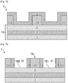
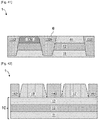
- the figure 1 is a sectional view of an example of structure 1 including an FDSOI substrate 10 configured to form nMOS and pMOS transistors according to a method which is the subject of the invention.
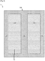
- the figure 2 is a top view of the same substrate 10.
- a substrate 10 is provided with a silicon layer 13, for example made of unintentionally doped silicon.
- the silicon layer 13 has a thickness typically between 5 and 20 nm, for example 6 nm.
- the silicon layer 13 is here formed on a buried insulating layer 12, for example made of SiO 2 , of a thickness typically between 15 and 40 nm, for example 25 nm.
- the buried insulation layer 12 is formed on a substrate 11, typically made of unintentionally doped silicon.
- a masking step (not shown) was carried out beforehand on the entire surface of the silicon layer 13, then a lithography step (not shown) to form a hard mask 14 on the silicon layer 13 , and finally in an etching step (not shown) according to the mask 14 previously formed.
- a strip of hard mask 140 is interposed between zones 151 and 152.
- Zone 151 is interposed between a strip 141 of hard mask and the strip 140.
- the zone 152 is interposed between a strip 142 of hard mask and the strip 140.
- the openings 51 and 52 for example have a width of at least 60 nm.
- the zones 151 and 152 made thus accessible constitute zones of formation of an nMOS transistor and a pMOS transistor respectively.
- the invention can be implemented from step 300, starting from the configuration illustrated in figures 1 and 2 .
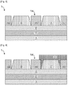
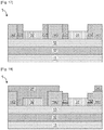
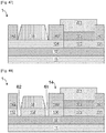
- a first deposit 17 of SiGe alloy is formed in the opening 51 in the zone 151, as illustrated in FIG. figure 3 .
- a second deposit 18 of SiGe alloy is simultaneously formed in the opening 52 in the zone 152.
- the deposits 17 and 18 are typically formed by growth by epitaxy with lateral facets. The lateral faces of the deposits 17 and 18 are thus inclined. Methods for growing SiGe by facet epitaxy are known per se to those skilled in the art.
- Deposits 17 and 18 typically have a thickness of between 5nm and 30nm.
- Deposits 17 and 18 include, for example, a concentration of Germanium (in quantity of atoms) of between 15 and 35%.
- the deposition by growth by epitaxy is for example carried out with SiGe containing 30% Germanium, at a temperature of 630 ° C. for example, using H 2 as carrier gas and Germane (GeH 4 ) and Dichlorosilane (DCS, SiH 2 Cl 2 ) as precursors (or silane SiH 4 ).
- the first deposit 17 is covered with a layer 21 of hard mask on the element 17, forming a protective layer, as illustrated in the figure 4 .
- the layer 21 is typically made of SiO 2 .
- This layer 21 has for example a thickness between 15nm and 40nm.
- step 303 a step of advantageously anisotropic etching of the second deposit 18 and of the layer 13 is implemented.
- the etching is stopped on the layer 12, to obtain the configuration illustrated in the figure 5 .
- This etching makes it possible to form grooves 61 and 62, which delimit layer 13 into an element 137 and zones 132 and 133. In this example, the same groove surrounds element 137.
- Layer 12 then forms the bottom of grooves 61 and 62.
- the superposition of the second deposit 18 and of the element of Si 137 forms a stack.
- the grooves 61 and 62, on either side of this stack typically have a width of between 1 and 10 nm.
- the etching of the grooves 61 and 62 is easily carried out because of the facets formed during the formation of the second deposit 18.
- the second deposit 18 thus has a decreasing thickness as one approaches the mask hard 14.
- the thickness of the deposit 18 may for example be substantially zero at its interface with the hard mask 14. The etching near the hard mask 14 thus makes it easy to reach the layer 12 around the second deposit 18.
- step 304 an ion implantation is carried out which deeply amorphizes the stack.
- the amorphization results in the formation of a layer 181 in amorphous SiGe.
- the amorphization leads to the formation of an element 138 in amorphous silicon.
- a layer 182 formed of a crystalline seed of non-amorphized SiGe is preserved.
- the crystal surface of element 137 is also preserved on element amorphous 138. This gives the configuration illustrated in figure 6 .
- the presence of grooves 61 and 62 on either side of the layer 182 allows the layer 182 not to undergo lateral stress and to adopt a relaxed stress state in a plane parallel to the layer 12.
- an annealing is carried out to obtain the recrystallization of the layer 181 as well as of the element 138.
- the annealing is for example carried out at a temperature of 600 ° C. to 700 ° C., advantageously maintained for 30 s to 5 min (depending on the thickness of the stack of SiGe / Si layers).
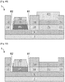
- the annealing operation makes it possible to obtain the configuration illustrated in the figure 7 , in which a layer 183 of relaxed SiGe has reformed over an element 139 of Si.
- the element 139 of Si then takes the mesh parameter of the layer 183 of relaxed SiGe and therefore becomes tension-constrained in a plane parallel to layer 12.
- step 306 the layer 183 of relaxed SiGe is removed by etching, which makes it possible to obtain the configuration illustrated in the figure 8 .
- the element 139 in Silicon retains a stress in tension in a plane parallel to the layer 12.
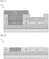
- a layer 22 of hard mask is formed on the element 139, as illustrated figure 9 .
- Layer 22 forms a protective layer.
- the element 139 is then protected during the subsequent etching steps.
- the second protective layer 22 is typically made of SiN. This layer 22 has for example a thickness between 30 and 50 nm. The thickness of the layer 22 formed is sufficient to exceed the top of the layer 21.
- step 308 an advantageously anisotropic etching step of the protective layer 21 and of the first deposit 17 is implemented.
- An element 171 of SiGe accessible through the opening 51 is thus formed. This gives the configuration illustrated in the figure 10 .
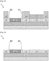
- step 310 the layer 173 of SiO 2 , the protective layer 22 and the strips 140, 141 and 142 are removed, as illustrated in FIG. figure 12 . Access to the SiGe element 172 on the one hand and to the element 139 on the other hand is thus provided.
- step 311 the elements 130, 131 and 132 are removed to form grooves by etching.
- the grooves are then filled with insulating material to form elements 1320, 1321 and 1322.
- Other areas of the structure may have a layer of unconstrained silicon for the formation of other transistors.
- Elements 172 and 139 are obtained from the same initial deposit of SiGe by epitaxy, with a reduced number of masking and photolithography steps.
- the figure 14 is a diagram illustrating the stages of the manufacturing process according to the first embodiment, as detailed above.
- the figure 15 is a sectional view of an exemplary structure 1 in a step of a manufacturing process, according to a second embodiment.
- An FDSOI 10 substrate is initially provided configured to form nMOS and pMOS transistors in accordance with figures 1 and 2 previously described.
- a uniform dielectric layer 23 was deposited in accordance with the upper surface of the structure 1.
- the layer 23 is for example made of SiO 2 , which makes it possible to perfectly control its thickness.
- a strip of hard mask 140 is interposed between the zones 151 and 152.
- a spacer 231, the remainder of the etching of the layer 23 and attached to the strip 140, is interposed between the strip 140 and the area 151.
- a spacer 234, residual of the etching of the layer 23 and attached to the strip 140, is interposed between the strip 140 and the zone 152.
- the zone 151 is interposed between a strip 141 of hard mask and the strip 140.
- the zone 152 is interposed between a strip 142 of hard mask and the strip 140.
- the openings 51 and 52 have for example a width of at least 40 nm.
- the zones 151 and 152 made thus accessible constitute zones of formation of an nMOS transistor and a pMOS transistor respectively.
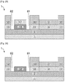
- a first deposit 31 of SiGe alloy as illustrated in the figure 17 .
- a second deposit 32 made of SiGe alloy is simultaneously formed in the opening 52 in the zone 152.
- the deposits 31 and 32 are typically formed by growth by epitaxy. Methods for growing SiGe by epitaxy are known per se to those skilled in the art. Deposits 31 and 32 typically have a thickness comprised between 5nm and 30nm. Deposits 31 and 32 include, for example, a concentration of Germanium (in quantity of atoms) of between 15 and 35%.
- the deposition by growth by epitaxy is for example carried out with SiGe containing 30% Germanium, at a temperature of 630 ° C. for example, using H 2 as carrier gas and Germane (GeH 4 ) and Dichlorosilane (DCS, SiH 2 Cl 2 ) as precursors (or silane SiH 4 ).
- the second deposit 32 is then covered with a layer 24 of hard mask.
- the layer 24 forms a protective layer.
- the layer 24 is here merged with the spacers 233 and 234, the layers 23 and 24 here being in the same material.
- the second deposit 32 is thus protected during the subsequent etching steps by this protective layer.
- a hard mask layer 241 is also deposited on the strip 141.
- the layers 24 and 241 are typically made of SiO 2 . These layers 24 and 241 have for example a thickness of between 10 and 40 nm.
- the upper surface of the element 34 is covered with a layer 33 of SiO 2 , obtained by thermal oxidation of the first deposit 31 and bonding with the spacers 231 and 232.
- the configuration obtained is illustrated in the figure 19 .
- Element 34 of SiGe retains the crystalline parameters of the original layer of Silicon 13.
- the condensation of Germanium in the silicon layer 13 leads to creating a biaxially compressive stress in a plane parallel to the insulating layer 12 in the element 34 formed.
- the boundary between element 34 and zones 131 and 134 is positioned substantially vertically lateral faces of the bands 141 and 140 respectively.
- the superposition of the element 34 and of the layer 33 forms a stack.
- Layer 25 is typically made of SOC type carbon or a hard mask enriched with silicon with hard anti-reflection mask.
- the layer 25 previously formed then undergoes an etching or mechanochemical polishing, with stopping on the hard mask layers 24 and 241, as illustrated in the figure 21 .
- the element 251 is thus formed, the remainder of the etching of the layer 25.
- the element 251 forms a protective layer and thus protects the layer 33 of SiO 2 and the element 34 of SiGe from the subsequent etching steps.
- the hard mask layers 24 and 241 are then removed by selective etching, thus freeing access to the second deposit 32 previously formed. This provides transient access to the second deposit 32. This etching is then continued to form grooves 610 and 620, which separate the second deposit 32 respectively from the strip 140 and the strip 142. The layer 134 then forms the bottom of the grooves 610 and 620. We obtain the configuration illustrated in figure 22 .
- an advantageously anisotropic etching step of the layer 134 is implemented, around the second deposit 32, stopped on the layer 12, to obtain the illustrated configuration. figure 23 .
- This engraving makes it possible to form the grooves 61 and 62, in the extension of the grooves 610 and 620.
- the grooves 61 and 62 separate an element 137 and zones 132 and 130. In this example, the same groove surrounds the element 137.
- the layer 12 then forms the bottom of the grooves 61 and 62.
- the superposition of the second deposit 32 and of the element 137 forms a stack called the second stack.
- the grooves 61 and 62 typically have a width of between 1 and 10 nm. In the present example, the etching of the grooves 61 and 62 is easily carried out due to the prior production of the grooves 610 and 620.
- the grooves 610 and 620 form a good starting point for easily reaching the layer 12 around the second deposit 32.
- the protective layer 251 is then removed.
- recrystallization annealing is also carried out to obtain the recrystallization of the layer 322 and of the layer 138.
- the annealing is for example carried out at a temperature of 600 ° C. to 700 ° C, advantageously maintained for 30 s to 5 min depending on the thickness of the SiGe / Si stack.
- the annealing operation makes it possible to obtain the configuration illustrated in the figure 25 , in which a layer 323 of relaxed SiGe has formed over an element 139 of crystalline Si.
- the element 139 of Si then takes the lattice parameter of the layer 323 of relaxed SiGe and therefore becomes tension-constrained in a plane parallel to the layer 12.
- the layer 323 of relaxed SiGe is then removed by etching, which makes it possible to obtain the configuration illustrated in the figure 26 .
- the element 139 in Silicon retains a stress in tension in a plane parallel to the layer 12.
- the elements 130, 131 and 132 are removed to form grooves by etching.
- the grooves are then filled with insulating material to form elements 1320, 1321 and 1322.
- STI Shallow Trench Isolation in English
- Other areas of the structure may have a layer of unconstrained silicon for the formation of other transistors.
- the figure 29 is a sectional view of an exemplary structure 1 in a step of a manufacturing process, according to a third embodiment.
- An FDSOI 10 substrate is initially provided configured to form nMOS and pMOS transistors in accordance with figures 1 and 2 previously described.
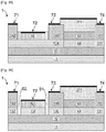
- a first deposit 41 of SiGe alloy was formed in the opening 51 in the zone 151, as illustrated in the figure 29 .
- a second deposit 42 of SiGe alloy was formed simultaneously in the opening 52 on the zone 152.
- Deposits 41 and 42 are typically formed by growth by epitaxy. Methods for growing SiGe by epitaxy are known per se to those skilled in the art. Deposits 41 and 42 typically have a thickness of between 5 nm and 30 nm. Deposits 41 and 42 include, for example, a concentration of Germanium (in quantity of atoms) of between 15 and 35%.
- the deposition by growth by epitaxy is for example carried out with SiGe containing 30% Germanium, at a temperature of 630 ° C. for example, using H 2 as carrier gas and Germane (GeH 4 ) and Dichlorosilane (DCS, SiH 2 Cl 2 ) as precursors (or silane SiH 4 ).
- the second deposit 42 is then covered with a layer of hard mask 26, forming a protective layer.
- the second deposit 42 is then protected during the subsequent etching steps.
- a hard mask layer 261 is also deposited on the strip 141.
- the layers 26 and 261 are typically made of SiO 2 . These layers 26 and 261 for example have a thickness between 10 and 40nm.
- the upper surface of the element 44 is covered with a layer 43 of SiO 2 , obtained by thermal oxidation of the first deposit 41.
- the configuration obtained is illustrated in the figure 31 .
- Element 44 of SiGe retains the mesh parameters of the original silicon layer 13 in its plane.
- the condensation of Germanium in the silicon layer 13 leads to creating a biaxially compressive stress in a plane parallel to the insulating layer 12 in the element 44 formed.
- the limit between the element 44 and the zones 131 and 134 is positioned substantially vertically of the lateral faces of the strips 141 and 140 respectively.
- the superposition of the element 44 and the layer 43 forms a stack.
- Layer 27 is typically made of SOC type carbon or a hard mask enriched with silicon with hard anti-reflection mask.
- the layer 27 previously formed then undergoes an etching or mechanochemical polishing, with stopping on the hard mask layers 26 and 261, as illustrated in the figure 33 .
- the element 271 is thus formed from the layer 27.
- the element 271 thus forms a protective layer, which thus protects the first stack from the subsequent etching steps.
- the hard mask layers 26 and 261 are then removed by selective etching, thus freeing access to the second deposit 42 previously formed, as illustrated in the figure 34 .
- an inclined implantation process is implemented, for example of species C (Carbon) or O (Oxygen) in at least 2 different inclined directions.
- the implantation can advantageously be carried out in 4 inclined directions, included in two perpendicular planes.
- the inclination makes it possible to benefit from a shading effect due to a higher height of the strips 140 and 142 relative to the deposit 42.
- the configuration illustrated in FIG. figure 35 the configuration illustrated in FIG. figure 35 .
- a high concentration of implanted ions is thus present in a zone 71 on the surface of the strip 142.
- a high concentration of implanted ions is also present in a zone 72 on the surface of the second deposit 42 and in a zone 73 on the surface.
- a high concentration of implanted ions is finally present in a zone 74 on the surface of the strip 141 as well as on the surface and on the lateral faces of the element 271.
- a step of advantageously anisotropic etching of the second deposit 42 and of the layer 13 is then implemented.
- the etching is stopped on the layer 12, in order to obtain the configuration illustrated in the figure 36 .
- This etching makes it possible to form an element 421, the residue of the second deposit 42.
- This etching also makes it possible to form grooves 61 and 62, which delimit layer 13 into an element 137 and zones 130 and 132. In this example, the same groove belt element 137.
- Layer 12 then forms the bottom of grooves 61 and 62.
- the superposition of elements 142 and 137 forms a stack.
- the grooves 61 and 62 typically have a width of between 1 and 10 nm. In the present example, the etching of the grooves 61 and 62 is easily carried out due to the initial absence of an implant on the surface of the second deposit 42 at the junction of said second deposit 42 and strips 140 on the one hand and 142 of somewhere else.
- the ion implantation also amorphizes element 137, which results in the formation of an element 138 in amorphous silicon.
- a layer 4211 formed of an unamorphized SiGe crystal seed is preserved. This gives the configuration illustrated in figure 37 .
- the presence of grooves 61 and 62 on either side of layer 4211 allows said layer 4211 not to be subjected to lateral stress and to adopt a relaxed stress state in a plane parallel to layer 12.
- the first protective layer 271 is then removed. Simultaneously, an annealing is also carried out for the recrystallization of the layer 4212 as well as of the element 138.
- the annealing is for example carried out at a temperature of 600 ° C. to 700 ° C, advantageously maintained for 30 seconds to 5 minutes depending on the thickness of the SiGe / Si stack.
- the annealing operation makes it possible to obtain the configuration illustrated in the figure 38 , in which a layer 4213 of relaxed SiGe is reformed over an element 139 of crystalline Si.
- the element 139 of Si then takes the mesh parameter of the layer 4213 of relaxed SiGe and therefore becomes tension-constrained in a plane parallel to the layer 12.
- the layer 4213 of relaxed SiGe is then removed by etching, which makes it possible to obtain the configuration illustrated in the figure 39 .
- the element 139 in Silicon retains a stress in tension in a plane parallel to the layer 12.
- the elements 130, 131 and 132 are removed to form grooves by etching.
- the grooves are then filled with insulating material to form elements 1320, 1321 and 1322.
- An insulation is thus formed between a first zone for forming pMOS transistors and a second zone for forming nMOS transistors.
- Other areas of the structure may have a layer of unconstrained silicon for the formation of other transistors.
- Elements 44 and 139 are obtained from the same initial deposit of SiGe by epitaxy, with a reduced number of masking and photolithography steps.
- the figure 42 is a sectional view of an exemplary structure 1 in a step of a manufacturing process, according to a fourth embodiment.
- An FDSOI 10 substrate is initially provided configured to form nMOS and pMOS transistors in accordance with figures 1 and 2 previously described.
- the order of masking of the areas of formation of the nMOS and pMOS transistors is reversed with respect to the first to third embodiments.
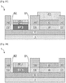
- a first deposit 17 of SiGe alloy was formed in the opening 51 in the zone 151, as illustrated in the figure 42 .
- a second deposit 18 made of SiGe alloy was formed simultaneously in the opening 52 on the zone 152.
- the deposits 17 and 18 are typically formed by growth by epitaxy with lateral facets. The lateral faces of the deposits 17 and 18 are thus inclined. Methods for growing SiGe by facet epitaxy are known per se to those skilled in the art.
- Deposits 17 and 18 typically have a thickness of between 5nm and 30nm.
- Deposits 17 and 18 include, for example, a concentration of Germanium (in quantity of atoms) of between 15 and 35%.
- the deposition by growth by epitaxy is for example carried out with SiGe containing 30% Germanium, at a temperature of 630 ° C. for example, using H 2 as carrier gas and Germane (GeH 4 ) and Dichlorosilane (DCS, SiH 2 Cl 2 ) as precursors (or silane SiH 4 ).
- the second deposit 18 is then covered with a layer 26 of hard mask.
- Layer 26 forms a protective layer.
- the second deposit 18 is thus protected during the subsequent etching steps.
- the strip 141 is also covered with a layer of hard mask 261.
- the layers 26 and 261 are typically made of SiO 2 . These layers 26 and 261 have for example a thickness of between 10 and 40 nm.
- a partial etching of the first deposit 17 is carried out, to result in the formation of an element 171, the thickness of which is advantageously between 5 and 15 nm.
- element 172 is covered with a layer 173 of SiO 2 , obtained by thermal oxidation of element 171.
- the configuration obtained is illustrated in figure 44 .
- the superposition of the element 172 and of the layer 173 forms a stack.
- Element 172 of SiGe retains the crystalline parameters of the original layer of Silicon 13.
- the condensation of Germanium in the silicon layer 13 leads to the creation of a biaxially compressive stress in a plane parallel to the insulating layer 12 in the element 172 formed.
- the limit between the element 172 and the zones 131 and 134 is positioned substantially vertically of the lateral faces of the strips 141 and 140 respectively.
- Layer 27 is typically made of SOC type carbon or a hard mask enriched with silicon with hard anti-reflection mask.
- the previously formed layer 27 then undergoes chemical mechanical etching or polishing, stopping on the hard mask layers 26 and 261, as illustrated in the figure 46 .
- the element 271 is thus formed, the residue of the layer 27.
- the element 271 forms a protective layer, which thus protects the layer 173 of SiO 2 and the element 172 of SiGe from the subsequent etching steps.
- the second protective layer 26 and the hard mask layer 261 are then removed by etching, thus freeing access to the second deposit 18 previously formed, as illustrated in FIG. figure 47 .
- a step of advantageously anisotropic etching of the second deposit 18 and of the layer 13 is then implemented.
- the etching is stopped on the layer 12, in order to obtain the configuration illustrated in the figure 48 .
- This etching makes it possible to form grooves 61 and 62, which delimit layer 13 into an element 137 and zones 130 and 132. In this example, the same groove surrounds element 137.
- Layer 12 then forms the bottom of grooves 61 and 62.
- the superposition of the second deposit 18 and of the element 137 forms a stack.
- the grooves 61 and 62 typically have a width of between 1 and 10 nm.
- the etching of the grooves 61 and 62 is easily carried out due to the facets formed during the formation of the second deposit 18.
- the second deposit 18 thus has a very small thickness near the hard mask 14.
- the etching near of the hard mask 14 thus makes it possible to easily reach the layer 12 around the second deposit 18.
- the amorphization of the second deposit 18 results in the formation of a layer 181 in amorphous SiGe.
- the amorphization of element 137 leads to the formation of an element 138 in amorphous silicon.
- a layer 182 formed of a crystalline seed of non-amorphized SiGe is preserved. This gives the configuration illustrated in figure 49 .
- the presence of grooves 61 and 62 on either side of the layer 182 allows said layer 182 not to undergo lateral stress and to adopt a relaxed stress state in a plane parallel to layer 12.
- An annealing is then carried out to obtain the recrystallization of the layer 181 as well as of the element 138.
- the annealing is for example carried out at a temperature of 600 ° C. to 700 ° C., advantageously maintained for 30 s to 5 min depending on the thickness. of the SiGe / Si stack.
- the annealing operation makes it possible to obtain the configuration illustrated in the figure 50 , in which a layer 183 of relaxed SiGe is reformed over an element 139 of crystalline Si.
- Element 139 of Si then takes the mesh parameter of the relaxed SiGe layer 183 and therefore becomes tension-constrained in a plane parallel to the layer 12.
- the layer 173 of SiO 2 and the bands 140, 141 and 142 are removed, as illustrated in FIG. figure 52 . Access to the SiGe element 172 on the one hand and to the Si element 139 on the other hand is thus provided.
- the elements 130, 131 and 132 are removed to form grooves by etching.
- the grooves are then filled with insulating material to form elements 1320, 1321 and 1322.
- STI Shallow Trench Isolation in English
- Other areas of the structure may have a layer of unconstrained silicon for the formation of other transistors.
- Elements 139 and 172 are obtained from the same initial deposit of SiGe by epitaxy, with a reduced number of masking and photolithography steps.
Landscapes
- Metal-Oxide And Bipolar Metal-Oxide Semiconductor Integrated Circuits (AREA)
- Insulated Gate Type Field-Effect Transistor (AREA)
Priority Applications (1)
| Application Number | Priority Date | Filing Date | Title |
|---|---|---|---|
| EP23175870.7A EP4235765B1 (de) | 2018-12-18 | 2019-12-11 | Verbessertes herstellungsverfahren eines integrierten schaltkreises, der einen nmos- und einen pmos-transistor umfasst |
Applications Claiming Priority (1)
| Application Number | Priority Date | Filing Date | Title |
|---|---|---|---|
| FR1873216A FR3090193B1 (fr) | 2018-12-18 | 2018-12-18 | Procédé amélioré de fabrication d’un circuit intégré comportant un transistor nMOS et un transistor pMOS |
Related Child Applications (1)
| Application Number | Title | Priority Date | Filing Date |
|---|---|---|---|
| EP23175870.7A Division EP4235765B1 (de) | 2018-12-18 | 2019-12-11 | Verbessertes herstellungsverfahren eines integrierten schaltkreises, der einen nmos- und einen pmos-transistor umfasst |
Publications (2)
| Publication Number | Publication Date |
|---|---|
| EP3671826A1 true EP3671826A1 (de) | 2020-06-24 |
| EP3671826B1 EP3671826B1 (de) | 2023-05-31 |
Family
ID=67185121
Family Applications (2)
| Application Number | Title | Priority Date | Filing Date |
|---|---|---|---|
| EP19215347.6A Active EP3671826B1 (de) | 2018-12-18 | 2019-12-11 | Verbessertes herstellungsverfahren eines integrierten schaltkreises, der einen nmos- und einen pmos-transistor umfasst |
| EP23175870.7A Active EP4235765B1 (de) | 2018-12-18 | 2019-12-11 | Verbessertes herstellungsverfahren eines integrierten schaltkreises, der einen nmos- und einen pmos-transistor umfasst |
Family Applications After (1)
| Application Number | Title | Priority Date | Filing Date |
|---|---|---|---|
| EP23175870.7A Active EP4235765B1 (de) | 2018-12-18 | 2019-12-11 | Verbessertes herstellungsverfahren eines integrierten schaltkreises, der einen nmos- und einen pmos-transistor umfasst |
Country Status (3)
| Country | Link |
|---|---|
| US (1) | US11217446B2 (de) |
| EP (2) | EP3671826B1 (de) |
| FR (1) | FR3090193B1 (de) |
Cited By (1)
| Publication number | Priority date | Publication date | Assignee | Title |
|---|---|---|---|---|
| EP4033517A1 (de) * | 2021-01-26 | 2022-07-27 | Commissariat à l'Energie Atomique et aux Energies Alternatives | Verfahren zur herstellung von zonen auf sige-basis mit unterschiedlichen ge-konzentrationen |
Citations (5)
| Publication number | Priority date | Publication date | Assignee | Title |
|---|---|---|---|---|
| EP1968103A1 (de) * | 2007-03-05 | 2008-09-10 | Commissariat A L'energie Atomique | Verfahren zur Herstellung eines Mischsubstrats und Verwendung für die Herstellung von CMOS-Schaltungen |
| US20120068267A1 (en) * | 2010-09-21 | 2012-03-22 | International Business Machines Corporation | Strained devices, methods of manufacture and design structures |
| EP2782118A1 (de) * | 2013-03-20 | 2014-09-24 | STMicroelectronics (Crolles 2) SAS | Verfahren zur Bildung einer Silizium-Spannschicht |
| US20150099335A1 (en) * | 2013-10-08 | 2015-04-09 | Stmicroelectronics, Inc. | Method of making a semiconductor device using trench isolation regions to maintain channel stress |
| US20170309483A1 (en) * | 2016-04-26 | 2017-10-26 | Commissariat A L'energie Atomique Et Aux Energies Alternatives | Manufacturing of silicon strained in tension on insulator by amorphisation then recrystallisation |
-
2018
- 2018-12-18 FR FR1873216A patent/FR3090193B1/fr active Active
-
2019
- 2019-12-11 EP EP19215347.6A patent/EP3671826B1/de active Active
- 2019-12-11 EP EP23175870.7A patent/EP4235765B1/de active Active
- 2019-12-17 US US16/716,687 patent/US11217446B2/en active Active
Patent Citations (5)
| Publication number | Priority date | Publication date | Assignee | Title |
|---|---|---|---|---|
| EP1968103A1 (de) * | 2007-03-05 | 2008-09-10 | Commissariat A L'energie Atomique | Verfahren zur Herstellung eines Mischsubstrats und Verwendung für die Herstellung von CMOS-Schaltungen |
| US20120068267A1 (en) * | 2010-09-21 | 2012-03-22 | International Business Machines Corporation | Strained devices, methods of manufacture and design structures |
| EP2782118A1 (de) * | 2013-03-20 | 2014-09-24 | STMicroelectronics (Crolles 2) SAS | Verfahren zur Bildung einer Silizium-Spannschicht |
| US20150099335A1 (en) * | 2013-10-08 | 2015-04-09 | Stmicroelectronics, Inc. | Method of making a semiconductor device using trench isolation regions to maintain channel stress |
| US20170309483A1 (en) * | 2016-04-26 | 2017-10-26 | Commissariat A L'energie Atomique Et Aux Energies Alternatives | Manufacturing of silicon strained in tension on insulator by amorphisation then recrystallisation |
Cited By (3)
| Publication number | Priority date | Publication date | Assignee | Title |
|---|---|---|---|---|
| EP4033517A1 (de) * | 2021-01-26 | 2022-07-27 | Commissariat à l'Energie Atomique et aux Energies Alternatives | Verfahren zur herstellung von zonen auf sige-basis mit unterschiedlichen ge-konzentrationen |
| FR3119268A1 (fr) * | 2021-01-26 | 2022-07-29 | Commissariat A L'energie Atomique Et Aux Energies Alternatives | Procédé de réalisation de zones à base de SiGe à différentes concentrations en Ge |
| US11854805B2 (en) | 2021-01-26 | 2023-12-26 | Commissariat A L'energie Atomique Et Aux Energies Alternatives | Method for producing SiGe-based zones at different concentrations of Ge |
Also Published As
| Publication number | Publication date |
|---|---|
| US20200203161A1 (en) | 2020-06-25 |
| FR3090193A1 (fr) | 2020-06-19 |
| EP4235765A2 (de) | 2023-08-30 |
| EP4235765B1 (de) | 2026-02-04 |
| EP4235765A3 (de) | 2023-10-11 |
| FR3090193B1 (fr) | 2020-11-27 |
| US11217446B2 (en) | 2022-01-04 |
| EP3671826B1 (de) | 2023-05-31 |
Similar Documents
| Publication | Publication Date | Title |
|---|---|---|
| EP1837916B1 (de) | Verfahren zum Herstellen eines Transistors mit einem Germanium enthaltenden Kanal | |
| US10566417B2 (en) | Self-forming spacers using oxidation | |
| US7791107B2 (en) | Strained tri-channel layer for semiconductor-based electronic devices | |
| EP3070744B1 (de) | Verbessertes herstellungsverfahren eines transistors in einem stapel von übereinander angeordneten halbleiterschichten | |
| FR2838237A1 (fr) | Procede de fabrication d'un transistor a effet de champ a grille isolee a canal contraint et circuit integre comprenant un tel transistor | |
| FR3060838A1 (fr) | Procede de realisation d'un dispositif semi-conducteur a canal contraint en compression | |
| EP2975646B1 (de) | Herstellungsverfahren eines transistors, in dem das an den kanal angelegte spannungsniveau erhöht ist | |
| EP2887384A1 (de) | Verbessertes Verfahren zur Herstellung von Halbleiterblöcken, die auf der Isolierschicht eines Halbleitersubstrats auf Isoliermaterial gespannt sind | |
| EP3142151B1 (de) | Herstellungsverfahren einer einachsig verspannten transistorkanalstruktur | |
| EP2835832A2 (de) | Verbessertes Verfahren zur Herstellung von dotierten Zonen und/oder Zonen, die eine Spannung unter den Abstandhaltern eines Transistors ausüben | |
| FR3005372A1 (fr) | Procede de realisation d'un film en silicium-germanium a teneur en germanium variable | |
| FR3023411A1 (fr) | Generation localisee de contrainte dans un substrat soi | |
| EP3079168A1 (de) | Dotierverfahren von source- und drain-bereichen eines transistors mithilfe einer selektiven amorphisierung | |
| EP3503175A1 (de) | Herstellungsverfahren eines halbleitersubstrats mit mindestens einem unter druckspannung stehenden halbleiterbereich | |
| EP1638149B1 (de) | Verfahren zur Herstellung eines Feldefekttransistors mit isoliertem Gatter und Heterostruktur-Kanal | |
| FR3088481A1 (fr) | Procede de fabrication d’un transistor a effet de champ a jonction alignee avec des espaceurs | |
| FR3050569A1 (fr) | Fabrication amelioree de silicium contraint en tension sur isolant par amorphisation puis recristallisation | |
| EP3026712B1 (de) | Verbessertes verfahren zur spannungsinduktion einer transistorkanalzone | |
| FR3048816A1 (fr) | Procede de fabrication d'un dispositif avec transistor nmos contraint en tension et transistor pmos contraint en compression uni-axiale | |
| EP3671826B1 (de) | Verbessertes herstellungsverfahren eines integrierten schaltkreises, der einen nmos- und einen pmos-transistor umfasst | |
| FR3048815A1 (fr) | Procede de co-realisation de zones sous contraintes uniaxiales differentes | |
| FR3046492A1 (fr) | Procede de realisation de transistors mos contraints | |
| EP1734568B1 (de) | Isolierter Transistor mit einem verspannten Kanal und Herstellungsverfahren | |
| FR3050315B1 (fr) | Transistor a overlap des regions d'acces maitrise | |
| FR2952225A1 (fr) | Procede de formation d'un transistor mos a canal en silicium-germanium |
Legal Events
| Date | Code | Title | Description |
|---|---|---|---|
| PUAI | Public reference made under article 153(3) epc to a published international application that has entered the european phase |
Free format text: ORIGINAL CODE: 0009012 |
|
| STAA | Information on the status of an ep patent application or granted ep patent |
Free format text: STATUS: REQUEST FOR EXAMINATION WAS MADE |
|
| 17P | Request for examination filed |
Effective date: 20191211 |
|
| AK | Designated contracting states |
Kind code of ref document: A1 Designated state(s): AL AT BE BG CH CY CZ DE DK EE ES FI FR GB GR HR HU IE IS IT LI LT LU LV MC MK MT NL NO PL PT RO RS SE SI SK SM TR |
|
| AX | Request for extension of the european patent |
Extension state: BA ME |
|
| GRAJ | Information related to disapproval of communication of intention to grant by the applicant or resumption of examination proceedings by the epo deleted |
Free format text: ORIGINAL CODE: EPIDOSDIGR1 |
|
| GRAP | Despatch of communication of intention to grant a patent |
Free format text: ORIGINAL CODE: EPIDOSNIGR1 |
|
| GRAP | Despatch of communication of intention to grant a patent |
Free format text: ORIGINAL CODE: EPIDOSNIGR1 |
|
| STAA | Information on the status of an ep patent application or granted ep patent |
Free format text: STATUS: GRANT OF PATENT IS INTENDED |
|
| RIC1 | Information provided on ipc code assigned before grant |
Ipc: H01L 21/8238 20060101ALI20221116BHEP Ipc: H01L 27/12 20060101ALI20221116BHEP Ipc: H01L 21/84 20060101AFI20221116BHEP |
|
| INTG | Intention to grant announced |
Effective date: 20221214 |
|
| GRAS | Grant fee paid |
Free format text: ORIGINAL CODE: EPIDOSNIGR3 |
|
| GRAA | (expected) grant |
Free format text: ORIGINAL CODE: 0009210 |
|
| STAA | Information on the status of an ep patent application or granted ep patent |
Free format text: STATUS: THE PATENT HAS BEEN GRANTED |
|
| AK | Designated contracting states |
Kind code of ref document: B1 Designated state(s): AL AT BE BG CH CY CZ DE DK EE ES FI FR GB GR HR HU IE IS IT LI LT LU LV MC MK MT NL NO PL PT RO RS SE SI SK SM TR |
|
| REG | Reference to a national code |
Ref country code: GB Ref legal event code: FG4D Free format text: NOT ENGLISH Ref country code: CH Ref legal event code: EP |
|
| REG | Reference to a national code |
Ref country code: DE Ref legal event code: R096 Ref document number: 602019029503 Country of ref document: DE |
|
| REG | Reference to a national code |
Ref country code: AT Ref legal event code: REF Ref document number: 1571474 Country of ref document: AT Kind code of ref document: T Effective date: 20230615 |
|
| REG | Reference to a national code |
Ref country code: IE Ref legal event code: FG4D Free format text: LANGUAGE OF EP DOCUMENT: FRENCH |
|
| REG | Reference to a national code |
Ref country code: LT Ref legal event code: MG9D |
|
| REG | Reference to a national code |
Ref country code: NL Ref legal event code: MP Effective date: 20230531 |
|
| REG | Reference to a national code |
Ref country code: AT Ref legal event code: MK05 Ref document number: 1571474 Country of ref document: AT Kind code of ref document: T Effective date: 20230531 |
|
| PG25 | Lapsed in a contracting state [announced via postgrant information from national office to epo] |
Ref country code: SE Free format text: LAPSE BECAUSE OF FAILURE TO SUBMIT A TRANSLATION OF THE DESCRIPTION OR TO PAY THE FEE WITHIN THE PRESCRIBED TIME-LIMIT Effective date: 20230531 Ref country code: NO Free format text: LAPSE BECAUSE OF FAILURE TO SUBMIT A TRANSLATION OF THE DESCRIPTION OR TO PAY THE FEE WITHIN THE PRESCRIBED TIME-LIMIT Effective date: 20230831 Ref country code: ES Free format text: LAPSE BECAUSE OF FAILURE TO SUBMIT A TRANSLATION OF THE DESCRIPTION OR TO PAY THE FEE WITHIN THE PRESCRIBED TIME-LIMIT Effective date: 20230531 Ref country code: AT Free format text: LAPSE BECAUSE OF FAILURE TO SUBMIT A TRANSLATION OF THE DESCRIPTION OR TO PAY THE FEE WITHIN THE PRESCRIBED TIME-LIMIT Effective date: 20230531 |
|
| PG25 | Lapsed in a contracting state [announced via postgrant information from national office to epo] |
Ref country code: RS Free format text: LAPSE BECAUSE OF FAILURE TO SUBMIT A TRANSLATION OF THE DESCRIPTION OR TO PAY THE FEE WITHIN THE PRESCRIBED TIME-LIMIT Effective date: 20230531 Ref country code: PL Free format text: LAPSE BECAUSE OF FAILURE TO SUBMIT A TRANSLATION OF THE DESCRIPTION OR TO PAY THE FEE WITHIN THE PRESCRIBED TIME-LIMIT Effective date: 20230531 Ref country code: NL Free format text: LAPSE BECAUSE OF FAILURE TO SUBMIT A TRANSLATION OF THE DESCRIPTION OR TO PAY THE FEE WITHIN THE PRESCRIBED TIME-LIMIT Effective date: 20230531 Ref country code: LV Free format text: LAPSE BECAUSE OF FAILURE TO SUBMIT A TRANSLATION OF THE DESCRIPTION OR TO PAY THE FEE WITHIN THE PRESCRIBED TIME-LIMIT Effective date: 20230531 Ref country code: LT Free format text: LAPSE BECAUSE OF FAILURE TO SUBMIT A TRANSLATION OF THE DESCRIPTION OR TO PAY THE FEE WITHIN THE PRESCRIBED TIME-LIMIT Effective date: 20230531 Ref country code: IS Free format text: LAPSE BECAUSE OF FAILURE TO SUBMIT A TRANSLATION OF THE DESCRIPTION OR TO PAY THE FEE WITHIN THE PRESCRIBED TIME-LIMIT Effective date: 20230930 Ref country code: HR Free format text: LAPSE BECAUSE OF FAILURE TO SUBMIT A TRANSLATION OF THE DESCRIPTION OR TO PAY THE FEE WITHIN THE PRESCRIBED TIME-LIMIT Effective date: 20230531 Ref country code: GR Free format text: LAPSE BECAUSE OF FAILURE TO SUBMIT A TRANSLATION OF THE DESCRIPTION OR TO PAY THE FEE WITHIN THE PRESCRIBED TIME-LIMIT Effective date: 20230901 |
|
| PG25 | Lapsed in a contracting state [announced via postgrant information from national office to epo] |
Ref country code: FI Free format text: LAPSE BECAUSE OF FAILURE TO SUBMIT A TRANSLATION OF THE DESCRIPTION OR TO PAY THE FEE WITHIN THE PRESCRIBED TIME-LIMIT Effective date: 20230531 |
|
| PG25 | Lapsed in a contracting state [announced via postgrant information from national office to epo] |
Ref country code: SK Free format text: LAPSE BECAUSE OF FAILURE TO SUBMIT A TRANSLATION OF THE DESCRIPTION OR TO PAY THE FEE WITHIN THE PRESCRIBED TIME-LIMIT Effective date: 20230531 |
|
| PG25 | Lapsed in a contracting state [announced via postgrant information from national office to epo] |
Ref country code: SM Free format text: LAPSE BECAUSE OF FAILURE TO SUBMIT A TRANSLATION OF THE DESCRIPTION OR TO PAY THE FEE WITHIN THE PRESCRIBED TIME-LIMIT Effective date: 20230531 Ref country code: SK Free format text: LAPSE BECAUSE OF FAILURE TO SUBMIT A TRANSLATION OF THE DESCRIPTION OR TO PAY THE FEE WITHIN THE PRESCRIBED TIME-LIMIT Effective date: 20230531 Ref country code: RO Free format text: LAPSE BECAUSE OF FAILURE TO SUBMIT A TRANSLATION OF THE DESCRIPTION OR TO PAY THE FEE WITHIN THE PRESCRIBED TIME-LIMIT Effective date: 20230531 Ref country code: PT Free format text: LAPSE BECAUSE OF FAILURE TO SUBMIT A TRANSLATION OF THE DESCRIPTION OR TO PAY THE FEE WITHIN THE PRESCRIBED TIME-LIMIT Effective date: 20231002 Ref country code: EE Free format text: LAPSE BECAUSE OF FAILURE TO SUBMIT A TRANSLATION OF THE DESCRIPTION OR TO PAY THE FEE WITHIN THE PRESCRIBED TIME-LIMIT Effective date: 20230531 Ref country code: DK Free format text: LAPSE BECAUSE OF FAILURE TO SUBMIT A TRANSLATION OF THE DESCRIPTION OR TO PAY THE FEE WITHIN THE PRESCRIBED TIME-LIMIT Effective date: 20230531 Ref country code: CZ Free format text: LAPSE BECAUSE OF FAILURE TO SUBMIT A TRANSLATION OF THE DESCRIPTION OR TO PAY THE FEE WITHIN THE PRESCRIBED TIME-LIMIT Effective date: 20230531 |
|
| REG | Reference to a national code |
Ref country code: DE Ref legal event code: R097 Ref document number: 602019029503 Country of ref document: DE |
|
| PLBE | No opposition filed within time limit |
Free format text: ORIGINAL CODE: 0009261 |
|
| STAA | Information on the status of an ep patent application or granted ep patent |
Free format text: STATUS: NO OPPOSITION FILED WITHIN TIME LIMIT |
|
| PG25 | Lapsed in a contracting state [announced via postgrant information from national office to epo] |
Ref country code: SI Free format text: LAPSE BECAUSE OF FAILURE TO SUBMIT A TRANSLATION OF THE DESCRIPTION OR TO PAY THE FEE WITHIN THE PRESCRIBED TIME-LIMIT Effective date: 20230531 |
|
| 26N | No opposition filed |
Effective date: 20240301 |
|
| PG25 | Lapsed in a contracting state [announced via postgrant information from national office to epo] |
Ref country code: SI Free format text: LAPSE BECAUSE OF FAILURE TO SUBMIT A TRANSLATION OF THE DESCRIPTION OR TO PAY THE FEE WITHIN THE PRESCRIBED TIME-LIMIT Effective date: 20230531 Ref country code: IT Free format text: LAPSE BECAUSE OF FAILURE TO SUBMIT A TRANSLATION OF THE DESCRIPTION OR TO PAY THE FEE WITHIN THE PRESCRIBED TIME-LIMIT Effective date: 20230531 |
|
| REG | Reference to a national code |
Ref country code: CH Ref legal event code: PL |
|
| PG25 | Lapsed in a contracting state [announced via postgrant information from national office to epo] |
Ref country code: LU Free format text: LAPSE BECAUSE OF NON-PAYMENT OF DUE FEES Effective date: 20231211 |
|
| PG25 | Lapsed in a contracting state [announced via postgrant information from national office to epo] |
Ref country code: MC Free format text: LAPSE BECAUSE OF FAILURE TO SUBMIT A TRANSLATION OF THE DESCRIPTION OR TO PAY THE FEE WITHIN THE PRESCRIBED TIME-LIMIT Effective date: 20230531 |
|
| REG | Reference to a national code |
Ref country code: BE Ref legal event code: MM Effective date: 20231231 |
|
| PG25 | Lapsed in a contracting state [announced via postgrant information from national office to epo] |
Ref country code: MC Free format text: LAPSE BECAUSE OF FAILURE TO SUBMIT A TRANSLATION OF THE DESCRIPTION OR TO PAY THE FEE WITHIN THE PRESCRIBED TIME-LIMIT Effective date: 20230531 Ref country code: LU Free format text: LAPSE BECAUSE OF NON-PAYMENT OF DUE FEES Effective date: 20231211 |
|
| REG | Reference to a national code |
Ref country code: IE Ref legal event code: MM4A |
|
| PG25 | Lapsed in a contracting state [announced via postgrant information from national office to epo] |
Ref country code: IE Free format text: LAPSE BECAUSE OF NON-PAYMENT OF DUE FEES Effective date: 20231211 |
|
| PG25 | Lapsed in a contracting state [announced via postgrant information from national office to epo] |
Ref country code: BE Free format text: LAPSE BECAUSE OF NON-PAYMENT OF DUE FEES Effective date: 20231231 |
|
| PG25 | Lapsed in a contracting state [announced via postgrant information from national office to epo] |
Ref country code: CH Free format text: LAPSE BECAUSE OF NON-PAYMENT OF DUE FEES Effective date: 20231231 |
|
| PG25 | Lapsed in a contracting state [announced via postgrant information from national office to epo] |
Ref country code: IE Free format text: LAPSE BECAUSE OF NON-PAYMENT OF DUE FEES Effective date: 20231211 Ref country code: CH Free format text: LAPSE BECAUSE OF NON-PAYMENT OF DUE FEES Effective date: 20231231 Ref country code: BE Free format text: LAPSE BECAUSE OF NON-PAYMENT OF DUE FEES Effective date: 20231231 |
|
| PG25 | Lapsed in a contracting state [announced via postgrant information from national office to epo] |
Ref country code: BG Free format text: LAPSE BECAUSE OF FAILURE TO SUBMIT A TRANSLATION OF THE DESCRIPTION OR TO PAY THE FEE WITHIN THE PRESCRIBED TIME-LIMIT Effective date: 20230531 |
|
| REG | Reference to a national code |
Ref country code: DE Ref legal event code: R079 Ref document number: 602019029503 Country of ref document: DE Free format text: PREVIOUS MAIN CLASS: H01L0021840000 Ipc: H10D0086010000 |
|
| PG25 | Lapsed in a contracting state [announced via postgrant information from national office to epo] |
Ref country code: BG Free format text: LAPSE BECAUSE OF FAILURE TO SUBMIT A TRANSLATION OF THE DESCRIPTION OR TO PAY THE FEE WITHIN THE PRESCRIBED TIME-LIMIT Effective date: 20230531 |
|
| PG25 | Lapsed in a contracting state [announced via postgrant information from national office to epo] |
Ref country code: CY Free format text: LAPSE BECAUSE OF FAILURE TO SUBMIT A TRANSLATION OF THE DESCRIPTION OR TO PAY THE FEE WITHIN THE PRESCRIBED TIME-LIMIT; INVALID AB INITIO Effective date: 20191211 |
|
| PG25 | Lapsed in a contracting state [announced via postgrant information from national office to epo] |
Ref country code: HU Free format text: LAPSE BECAUSE OF FAILURE TO SUBMIT A TRANSLATION OF THE DESCRIPTION OR TO PAY THE FEE WITHIN THE PRESCRIBED TIME-LIMIT; INVALID AB INITIO Effective date: 20191211 |
|
| PG25 | Lapsed in a contracting state [announced via postgrant information from national office to epo] |
Ref country code: TR Free format text: LAPSE BECAUSE OF FAILURE TO SUBMIT A TRANSLATION OF THE DESCRIPTION OR TO PAY THE FEE WITHIN THE PRESCRIBED TIME-LIMIT Effective date: 20230531 |
|
| PGFP | Annual fee paid to national office [announced via postgrant information from national office to epo] |
Ref country code: GB Payment date: 20251229 Year of fee payment: 7 |
|
| PGFP | Annual fee paid to national office [announced via postgrant information from national office to epo] |
Ref country code: FR Payment date: 20251222 Year of fee payment: 7 |
|
| PGFP | Annual fee paid to national office [announced via postgrant information from national office to epo] |
Ref country code: DE Payment date: 20251222 Year of fee payment: 7 |