US11217446B2 - Method for fabricating an integrated circuit including a NMOS transistor and a PMOS transistor - Google Patents
Method for fabricating an integrated circuit including a NMOS transistor and a PMOS transistor Download PDFInfo
- Publication number
- US11217446B2 US11217446B2 US16/716,687 US201916716687A US11217446B2 US 11217446 B2 US11217446 B2 US 11217446B2 US 201916716687 A US201916716687 A US 201916716687A US 11217446 B2 US11217446 B2 US 11217446B2
- Authority
- US
- United States
- Prior art keywords
- deposit
- layer
- region
- silicon layer
- hard mask
- Prior art date
- Legal status (The legal status is an assumption and is not a legal conclusion. Google has not performed a legal analysis and makes no representation as to the accuracy of the status listed.)
- Active, expires
Links
Images





Classifications
-
- H—ELECTRICITY
- H10—SEMICONDUCTOR DEVICES; ELECTRIC SOLID-STATE DEVICES NOT OTHERWISE PROVIDED FOR
- H10P—GENERIC PROCESSES OR APPARATUS FOR THE MANUFACTURE OR TREATMENT OF DEVICES COVERED BY CLASS H10
- H10P14/00—Formation of materials, e.g. in the shape of layers or pillars
- H10P14/20—Formation of materials, e.g. in the shape of layers or pillars of semiconductor materials
- H10P14/29—Formation of materials, e.g. in the shape of layers or pillars of semiconductor materials characterised by the substrates
- H10P14/2901—Materials
- H10P14/2902—Materials being Group IVA materials
- H10P14/2905—Silicon, silicon germanium or germanium
-
- H01L21/02381—
-
- H01L21/02488—
-
- H01L21/02532—
-
- H01L21/02694—
-
- H01L21/823807—
-
- H01L21/84—
-
- H—ELECTRICITY
- H10—SEMICONDUCTOR DEVICES; ELECTRIC SOLID-STATE DEVICES NOT OTHERWISE PROVIDED FOR
- H10D—INORGANIC ELECTRIC SEMICONDUCTOR DEVICES
- H10D84/00—Integrated devices formed in or on semiconductor substrates that comprise only semiconducting layers, e.g. on Si wafers or on GaAs-on-Si wafers
- H10D84/01—Manufacture or treatment
- H10D84/0123—Integrating together multiple components covered by H10D12/00 or H10D30/00, e.g. integrating multiple IGBTs
- H10D84/0126—Integrating together multiple components covered by H10D12/00 or H10D30/00, e.g. integrating multiple IGBTs the components including insulated gates, e.g. IGFETs
- H10D84/0165—Integrating together multiple components covered by H10D12/00 or H10D30/00, e.g. integrating multiple IGBTs the components including insulated gates, e.g. IGFETs the components including complementary IGFETs, e.g. CMOS devices
- H10D84/0167—Manufacturing their channels
-
- H—ELECTRICITY
- H10—SEMICONDUCTOR DEVICES; ELECTRIC SOLID-STATE DEVICES NOT OTHERWISE PROVIDED FOR
- H10D—INORGANIC ELECTRIC SEMICONDUCTOR DEVICES
- H10D84/00—Integrated devices formed in or on semiconductor substrates that comprise only semiconducting layers, e.g. on Si wafers or on GaAs-on-Si wafers
- H10D84/01—Manufacture or treatment
- H10D84/02—Manufacture or treatment characterised by using material-based technologies
- H10D84/03—Manufacture or treatment characterised by using material-based technologies using Group IV technology, e.g. silicon technology or silicon-carbide [SiC] technology
- H10D84/038—Manufacture or treatment characterised by using material-based technologies using Group IV technology, e.g. silicon technology or silicon-carbide [SiC] technology using silicon technology, e.g. SiGe
-
- H—ELECTRICITY
- H10—SEMICONDUCTOR DEVICES; ELECTRIC SOLID-STATE DEVICES NOT OTHERWISE PROVIDED FOR
- H10D—INORGANIC ELECTRIC SEMICONDUCTOR DEVICES
- H10D86/00—Integrated devices formed in or on insulating or conducting substrates, e.g. formed in silicon-on-insulator [SOI] substrates or on stainless steel or glass substrates
- H10D86/01—Manufacture or treatment
-
- H—ELECTRICITY
- H10—SEMICONDUCTOR DEVICES; ELECTRIC SOLID-STATE DEVICES NOT OTHERWISE PROVIDED FOR
- H10D—INORGANIC ELECTRIC SEMICONDUCTOR DEVICES
- H10D86/00—Integrated devices formed in or on insulating or conducting substrates, e.g. formed in silicon-on-insulator [SOI] substrates or on stainless steel or glass substrates
- H10D86/201—Integrated devices formed in or on insulating or conducting substrates, e.g. formed in silicon-on-insulator [SOI] substrates or on stainless steel or glass substrates the substrates comprising an insulating layer on a semiconductor body, e.g. SOI
-
- H—ELECTRICITY
- H10—SEMICONDUCTOR DEVICES; ELECTRIC SOLID-STATE DEVICES NOT OTHERWISE PROVIDED FOR
- H10P—GENERIC PROCESSES OR APPARATUS FOR THE MANUFACTURE OR TREATMENT OF DEVICES COVERED BY CLASS H10
- H10P14/00—Formation of materials, e.g. in the shape of layers or pillars
- H10P14/20—Formation of materials, e.g. in the shape of layers or pillars of semiconductor materials
- H10P14/32—Formation of materials, e.g. in the shape of layers or pillars of semiconductor materials characterised by intermediate layers between substrates and deposited layers
- H10P14/3202—Materials thereof
- H10P14/3238—Materials thereof being insulating materials
-
- H—ELECTRICITY
- H10—SEMICONDUCTOR DEVICES; ELECTRIC SOLID-STATE DEVICES NOT OTHERWISE PROVIDED FOR
- H10P—GENERIC PROCESSES OR APPARATUS FOR THE MANUFACTURE OR TREATMENT OF DEVICES COVERED BY CLASS H10
- H10P14/00—Formation of materials, e.g. in the shape of layers or pillars
- H10P14/20—Formation of materials, e.g. in the shape of layers or pillars of semiconductor materials
- H10P14/34—Deposited materials, e.g. layers
- H10P14/3402—Deposited materials, e.g. layers characterised by the chemical composition
- H10P14/3404—Deposited materials, e.g. layers characterised by the chemical composition being Group IVA materials
- H10P14/3411—Silicon, silicon germanium or germanium
-
- H—ELECTRICITY
- H10—SEMICONDUCTOR DEVICES; ELECTRIC SOLID-STATE DEVICES NOT OTHERWISE PROVIDED FOR
- H10P—GENERIC PROCESSES OR APPARATUS FOR THE MANUFACTURE OR TREATMENT OF DEVICES COVERED BY CLASS H10
- H10P14/00—Formation of materials, e.g. in the shape of layers or pillars
- H10P14/20—Formation of materials, e.g. in the shape of layers or pillars of semiconductor materials
- H10P14/38—Formation of materials, e.g. in the shape of layers or pillars of semiconductor materials characterised by treatments done after the formation of the materials
- H10P14/3822—Controlling the interface between substrate and epitaxial layer, e.g. by ion implantation followed by annealing
Definitions
- the invention relates to the fabrication of silicon-on-insulator transistors, and in particular to the fabrication of silicon-on-insulator transistors having improved carrier-mobility properties in the channels thereof.
- the STRASS process includes depositing SiGe on a silicon layer, relaxing the SiGe and amorphizing the lower portion thereof and the silicon layer. Next, the SiGe layer is recrystallized from its top and the silicon layer is recrystallized in order to tensilely strain it. After removal of the SiGe layer, the silicon layer remains tensilely strained.
- the invention aims to solve one or more of these drawbacks.
- the invention thus relates to a process for fabricating an integrated circuit, such as defined in the appended claims.
- the invention also relates to the variants of the dependent claims. Those skilled in the art will understand that any of the features of the description or of the dependent claims may be combined independently with the features of an independent claim, without however constituting an intermediate generalization.
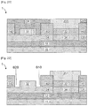
- FIG. 1 and 1 are identical to FIG. 1 and 1;
- FIG. 2 are respectively views in cross section and from above of an FDSOI (fully-depleted silicon-on-insulator) substrate intended to form an nMOS transistor and a pMOS transistor;
- FDSOI fully-depleted silicon-on-insulator
- FIG. 3
- FIG. 4
- FIG. 5
- FIG. 6
- FIG. 7
- FIG. 8
- FIG. 9
- FIG. 10
- FIG. 11
- FIG. 12 and
- FIG. 13 are views in cross section of said nMOS and pMOS transistors at various stages of their fabricating process according to a first embodiment
- FIG. 14 is a diagram illustrating the steps of the fabricating process according to the first embodiment
- FIG. 15
- FIG. 16
- FIG. 17
- FIG. 18
- FIG. 19
- FIG. 20
- FIG. 21 is a diagrammatic representation of FIG. 21 .
- FIG. 22
- FIG. 23
- FIG. 24
- FIG. 25
- FIG. 26
- FIG. 28 are views in cross section of said nMOS and pMOS transistors at various stages of their fabricating process according to a second embodiment
- FIG. 29 is a diagrammatic representation of FIG. 29 .
- FIG. 30
- FIG. 31
- FIG. 32
- FIG. 33
- FIG. 34
- FIG. 35
- FIG. 36
- FIG. 37
- FIG. 38
- FIG. 39
- FIG. 41 are views in cross section of said nMOS and pMOS transistors at various stages of their fabricating process according to a third embodiment
- FIG. 42
- FIG. 43
- FIG. 44
- FIG. 45
- FIG. 46
- FIG. 47
- FIG. 48
- FIG. 49 is a diagrammatic representation of FIG. 49 .
- FIG. 50
- FIG. 51 is a diagrammatic representation of FIG. 51 .
- FIG. 52 and
- FIG. 53 are views in cross section of said nMOS and pMOS transistors at various stages of their fabricating process according to a fourth embodiment.
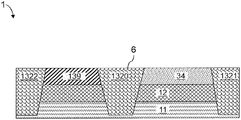
- FIG. 1 is a view in cross section of an example of a structure 1 including an FDSOI substrate 10 configured to form nMOS and pMOS transistors using a process according to the invention.
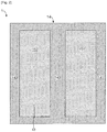
- FIG. 2 is a view from above of the same substrate 10 .
- a substrate 10 equipped with a silicon layer 13 for example made of unintentionally doped silicon.
- the silicon layer 13 has a thickness typically comprised between 5 and 20 nm, and for example of 6 nm.
- the silicon layer 13 is here formed on a layer of buried insulator 12 , which is for example made of SiO 2 , of a thickness typically comprised between 15 and 40 nm, and for example of 25 nm.
- the buried layer of insulator 12 is formed on a substrate 11 , which is typically made of unintentionally doped silicon.
- a step of masking (not shown) the entirety of the surface of the silicon layer 13 , then a step of lithography (not shown) in order to form a hard mask 14 on the silicon layer 13 , and lastly an etching step (not shown) in order to transfer the pattern of the mask 14 formed beforehand.
- a strip of hard mask 140 is interposed between the regions 151 and 152 .
- the region 151 is interposed between a strip 141 of hard mask and the strip 140 .
- the region 152 is interposed between a strip 142 of hard mask and the strip 140 .
- the apertures 51 and 52 for example have a width of at least 60 nm.
- the regions 151 and 152 thus made accessible form regions for forming an nMOS transistor and a pMOS transistor, respectively.
- the invention may be implemented from step 300 , starting with the configuration illustrated in FIGS. 1 and 2 .
- a first deposit 17 of SiGe alloy is formed in the aperture 51 on the region 151 as illustrated in FIG. 3 .
- a second deposit 18 of SiGe alloy is simultaneously formed in the aperture 52 on the region 152 .
- the deposits 17 and 18 are typically formed by epitaxial growth with lateral facets. The lateral faces of the deposits 17 and 18 are thus inclined. Processes for growing SiGe epitaxially with facets are known per se to those skilled in the art.
- the deposits 17 and 18 typically have a thickness comprised between 5 nm and 30 nm.
- the deposits 17 and 18 for example have a germanium concentration (in number of atoms) comprised between and 35%.
- the epitaxially grown deposit is for example SiGe containing 30% germanium, grown at a temperature of 630° C. for example using H 2 as vector gas and germane (GeH 4 ) and dichlorosilane (DCS, SiH 2 Cl 2 ) as precursors (or silane SiH 4 ).
- H 2 vector gas and germane
- DCS, SiH 2 Cl 2 dichlorosilane
- the first deposit 17 is covered with a layer 21 of hard mask on the element 17 , forming a protective layer, as illustrated in FIG. 4 .
- the layer 21 is typically made of SiO 2 .
- This layer 21 for example has a thickness comprised between nm and 40 nm.
- a step of etching the second deposit 18 and the layer 13 advantageously anisotropically is carried out.
- the etch is stopped on the layer 12 , in order to obtain the configuration illustrated in FIG. 5 .
- This etching allows trenches 61 and 62 , which divide the layer 13 into an element 137 and regions 132 and 133 , to be formed. In this example, a single trench encircles the element 137 .
- the layer 12 then forms the bottom of the trenches 61 and 62 .
- the superposition of the second deposit 18 and of the Si element 137 forms a stack.
- the trenches 61 and 62 on either side of this stack, typically have a width comprised between 1 and 10 nm.
- the trenches 61 and 62 are easily etched because of the facets formed during the formation of the second deposit 18 .
- the second deposit 18 thus has a thickness that decreases as the distance to the hard mask 14 decreases.
- the thickness of the deposit 18 may for example be substantially zero at its interface with the hard mask 14 . Etching in proximity to the hard mask 14 thus allows the layer 12 to be easily reached around the second deposit 18 .
- step 304 an ion implantation is carried out that amorphizes the stack depthwise.
- the amorphization forms a layer 181 made of amorphous SiGe.
- the amorphization forms an element 138 made of amorphous silicon.
- a layer 182 formed from a crystalline seed of non-amorphized SiGe is preserved.
- the crystalline surface of the element 137 is also preserved on the amorphous element 138 .
- the configuration illustrated in FIG. 6 is obtained.
- the presence of the trenches 61 and 62 on either side of the layer 182 allows the layer 182 to not undergo lateral strain and to adopt a relaxed strain state in a plane parallel to the layer 12 .
- an anneal is carried out in order to recrystallize the layer 181 and the element 138 .
- the anneal is for example carried out at a temperature of 600° C. to 700° C., advantageously maintained for 30 s to 5 min (depending on the thickness of the stack of SiGe/Si layers).
- the annealing operation allows the configuration illustrated in FIG. 7 to be obtained, in which a layer 183 of relaxed SiGe has been reformed above an Si element 139 .
- the Si element 139 then takes the lattice parameter of the relaxed SiGe layer 183 and therefore becomes tensilely strained in a plane parallel to the layer 12 .
- step 306 the relaxed SiGe layer 183 is removed by etching, this allowing the configuration illustrated in FIG. 8 to be obtained.
- the element 139 made of silicon preserves a tensile strain in a plane parallel to the layer 12 .
- a layer 22 of hard mask is formed on the element 139 , as illustrated in FIG. 9 .
- the layer 22 forms a protective layer.
- the element 139 is then protected during subsequent etching steps.
- the second protective layer 22 is typically made of SiN. This layer 22 for example has a thickness comprised between 30 and 50 nm. The thickness of the layer 22 formed is sufficient to bypass the top of the layer 21 .
- step 308 a step of etching the protective layer 21 and the first deposit 17 advantageously anisotropically is carried out.
- An SiGe element 171 that is accessible via the aperture 51 is thus formed. The configuration illustrated in FIG. 10 is thus obtained.
- step 309 a thermally oxidizing anneal of the SiGe element 171 is carried out.
- This anneal causes germanium to diffuse from the element 171 into the silicon layer 13 , this leading to the formation, in the layer 13 , of the following elements:
- step 310 the SiO 2 layer 173 , the protective layer 22 and the strips 140 , 141 and 142 are removed, as illustrated in FIG. 12 .
- access is obtained to the SiGe element 172 on the one hand and to the element 139 on the other hand.
- step 311 the elements 130 , 131 and 132 are removed in order to form trenches by etching.
- the trenches are then filled with insulator in order to form the elements 1320 , 1321 and 1322 .
- This allows shallow trench isolations to be formed, as illustrated in FIG. 13 .
- an isolation is formed between a region for forming pMOS transistors and a region for forming nMOS transistors.
- Other regions of the structure may have an un-strained silicon layer for forming other transistors.
- the elements 172 and 139 are obtained from an initial deposit of SiGe formed by epitaxy, with a low number of masking and photolithography steps.
- FIG. 14 is a diagram illustrating the steps of the fabricating process according to the first embodiment, as detailed above.
- FIG. 15 is a view in cross section of an example of a structure 1 at a stage of a fabricating process according to a second embodiment. Initially, an FDSOI substrate 10 configured to form nMOS and pMOS transistors in accordance with FIGS. 1 and 2 described above is provided.
- a dielectric layer 23 is conformally deposited uniformly over the upper surface of the structure 1 .
- the layer 23 is for example made of SiO 2 , this allowing its thickness to be perfectly controlled.
- the layer 23 is etched, advantageously using an anisotropic plasma etch of fluorocarbon chemistry, as illustrated in FIG. 16 .
- This allows apertures 51 and 52 to be opened and the associated regions 151 and 152 of the silicon layer 13 at the bottom of the apertures 51 and 52 to be uncovered.
- a strip of hard mask 140 is interposed between the regions 151 and 152 .
- a spacer 231 left over by the etch of the layer 23 and attached to the strip 140 , is interposed between the strip 140 and the region 151 .
- a spacer 234 left over by the etch of the layer 23 and attached to the strip 140 , is interposed between the strip 140 and the region 152 .
- the region 151 is interposed between a strip 141 of hard mask and the strip 140 .
- a spacer 232 left over by the etch of the layer 23 and attached to the strip 141 , is interposed between the strip 141 and the region 151 .
- the region 152 is interposed between a strip 142 of hard mask and the strip 140 .
- a spacer 233 left over by the etch of the layer 23 and attached to the strip 142 , is interposed between the strip 142 and the region 152 .
- the apertures 51 and 52 for example have a width of at least 40 nm.
- the regions 151 and 152 thus made accessible form regions for forming an nMOS transistor and a pMOS transistor, respectively.
- a first deposit 31 of SiGe alloy is formed, as illustrated in FIG. 17 .
- a second deposit 32 of SiGe alloy is simultaneously formed in the aperture 52 on the region 152 .
- the deposits 31 and 32 are typically formed by epitaxial growth. Processes for growing SiGe epitaxially are known per se to those skilled in the art.
- the deposits 31 and 32 typically have a thickness comprised between 5 nm and 30 nm.
- the deposits 31 and 32 for example have a germanium concentration (in number of atoms) comprised between 15 and 35%.
- the epitaxially grown deposit is for example SiGe containing 30% germanium, grown at a temperature of 630° C. for example using H 2 as vector gas and germane (GeH 4 ) and dichlorosilane (DCS, SiH 2 Cl 2 ) as precursors (or silane SiH 4 ).
- the second deposit 32 is then covered with a layer 24 of hard mask.
- the layer 24 forms a protective layer.
- the layer 24 here merges with the spacers 233 and 234 , the layers 23 and 24 being made of the same material.
- the second deposit 32 is thus protected during the subsequent etching steps by this protective layer.
- a layer of hard mask 241 is also deposited on the strip 141 .
- the layers 24 and 241 are typically made of SiO 2 . These layers 24 and 241 for example have a thickness comprised between 10 and 40 nm.
- a thermally oxidizing anneal of the first SiGe deposit 31 is then carried out. This anneal causes germanium to diffuse from the first deposit 31 into the silicon layer 13 , this leading to the formation, in said layer 13 , of the following elements:
- the upper surface of the element 34 is covered by a layer 33 of SiO 2 obtained via thermal oxidation of the first deposit 31 and linking with the spacers 231 and 232 .
- the obtained configuration is illustrated in FIG. 19 .
- the SiGe element 34 preserves the lattice parameters of the original silicon layer 13 .
- the condensation of the germanium into the silicon layer 13 leads to the creation of a biaxial compressive strain in a plane parallel to the layer of insulator 12 in the element 34 formed.
- the limit between the element 34 and the regions 131 and 134 is positioned substantially plumb with the lateral faces of the strips 141 and 140 , respectively.
- the superposition of the element 34 and of the layer 33 forms a stack.
- a layer 25 is then deposited on the wafer scale.
- the layer 25 is typically made of spin-on carbon (SoC) or an antireflective silicon-enriched hard mask.
- the layer 25 formed precedingly then undergoes an etch or chemical-mechanical polish, which is stopped on the layers of hard mask 24 and 241 , as illustrated in FIG. 21 .
- the element 251 left over by the etch of the layer 25 , is thus formed.
- the element 251 forms a protective layer and thus protects the SiO 2 layer 33 and the SiGe element 34 from the subsequent etching steps.
- the layers of hard mask 24 and 241 are then removed by selective etching, thus unblocking access to the second deposit 32 formed beforehand. Thus, temporarily, access to the second deposit 32 is possible. This etch is then continued to form trenches 610 and 620 , which separate the second deposit 32 from the strip 140 and from the strip 142 , respectively. The layer 134 then forms the bottom of the trenches 610 and 620 .
- the configuration illustrated in FIG. 22 is obtained.
- a step of etching the layer 134 around the second deposit 32 advantageously anisotropically is then carried out, this etch is stopped on the layer 12 , in order to obtain the configuration illustrated in FIG. 23 .
- This etching allows trenches 61 and 62 to be formed in the extension of the trenches 610 and 620 .
- the trenches 61 and 62 separate an element 137 and regions 132 and 130 . In this example, a single trench encircles the element 137 .
- the layer 12 then forms the bottom of the trenches 61 and 62 .
- the superposition of the second deposit 32 and of the element 137 forms a stack called the second stack.
- the trenches 61 and 62 typically have a width comprised between 1 and 10 nm. In the present example, the trenches 61 and 62 are easily etched because of the trenches 610 and 620 produced beforehand. The trenches 610 and 620 form a good starting point allowing the layer 12 to easily be reached
- an ion implantation is carried out that amorphizes the stack of the deposit 32 and of the element 137 depthwise. From the deposit 32 , the amorphization forms a layer 322 made of amorphous SiGe. From the element 137 , the amorphization forms an element 138 made of amorphous silicon. On the surface of the deposit 32 , a layer 321 formed from a crystalline seed of non-amorphized SiGe is preserved. Thus, the configuration illustrated in FIG. 24 is obtained. The presence of the trenches 61 and 62 on either side of the layer 321 allows said layer 321 to not undergo lateral strain and to adopt a relaxed strain state in a plane parallel to the layer 12 .
- the protective layer 251 is then removed. Simultaneously, a recrystallisation anneal is also carried out in order to recrystallize the layer 322 and the layer 138 .
- the anneal is for example carried out at a temperature of 600° C. to 700° C., advantageously maintained for 30 s to 5 min depending on the thickness of the SiGe/Si stack.
- the annealing operation allows the configuration illustrated in FIG. to be obtained, in which a layer 323 of relaxed SiGe has been formed above a crystalline Si element 139 .
- the Si element 139 then takes the lattice parameter of the relaxed SiGe layer 323 and therefore becomes tensilely strained in a plane parallel to the layer 12 .
- the relaxed SiGe layer 323 is removed by etching, this allowing the configuration illustrated in FIG. 26 to be obtained.
- the element 139 made of silicon preserves a tensile strain in a plane parallel to the layer 12 .
- the SiO 2 layer 33 and the strips 140 , 141 and 142 are then removed. Access on the one hand to the element 139 made of silicon and on the other hand to the element 34 made of SiGe is thus achieved.
- the elements 130 , 131 and 132 are removed in order to form trenches by etching.
- the trenches are then filled with insulator in order to form the elements 1320 , 1321 and 1322 .
- This allows shallow trench isolations to be formed, as illustrated in FIG. 28 .
- an isolation is formed between a first region for forming pMOS transistors and a second region for forming nMOS transistors.
- Other regions of the structure may have an un-strained silicon layer for forming other transistors.
- FIG. 29 is a view in cross section of an example of a structure 1 at a stage of a fabricating process according to a third embodiment. Initially, an FDSOI substrate configured to form nMOS and pMOS transistors in accordance with FIGS. 1 and 2 described above is provided.
- a first deposit 41 of SiGe alloy is formed in the aperture 51 on the region 151 as illustrated in FIG. 29 .
- a second deposit 42 of SiGe alloy is simultaneously formed in the aperture 52 on the region 152 .
- the deposits 41 and 42 are typically formed by epitaxial growth. Processes for growing SiGe epitaxially are known per se to those skilled in the art.
- the deposits 41 and 42 typically have a thickness comprised between 5 nm and 30 nm.
- the deposits 41 and 42 for example have a germanium concentration (in number of atoms) comprised between 15 and 35%.
- the epitaxially grown deposit is for example SiGe containing 30% germanium, grown at a temperature of 630° C. for example using H 2 as vector gas and germane (GeH 4 ) and dichlorosilane (DCS, SiH 2 Cl 2 ) as precursors (or silane SiH 4 ).
- the second deposit 42 is then covered with a layer 26 of hard mask, forming a protective layer.
- the second deposit 42 is then protected during the subsequent etching steps.
- a layer of hard mask 261 is also deposited on the strip 141 .
- the layers 26 and 261 are typically made of SiO 2 . These layers 26 and 261 for example have a thickness comprised between 10 and 40 nm.
- a thermally oxidizing anneal of the first SiGe deposit 41 is then carried out. This anneal causes germanium to diffuse from the first deposit 41 into the silicon layer 13 , this leading to the formation, in said layer 13 , of the following elements:
- the upper surface of the element 44 is covered by a layer 43 of SiO 2 obtained via thermal oxidation of the first deposit 41 .
- the obtained configuration is illustrated in FIG. 31 .
- the SiGe element 44 preserves the lattice parameters of the original silicon layer 13 in its plane.
- the condensation of the germanium into the silicon layer 13 leads to the creation of a biaxial compressive strain in a plane parallel to the layer of insulator 12 in the element 44 formed.
- the limit between the element 44 and the regions 131 and 134 is positioned substantially plumb with the lateral faces of the strips 141 and 140 , respectively.
- the superposition of the element 44 and of the layer 43 forms a stack.
- a layer 27 is then deposited on the wafer scale.
- the layer 27 is typically made of spin-on carbon (SoC) or an antireflective silicon-enriched hard mask.
- the layer 27 formed precedingly then undergoes an etch or chemical-mechanical polish, which is stopped on the layers of hard mask 26 and 261 , as illustrated in FIG. 33 .
- the element 271 is thus formed from the layer 27 .
- the element 271 thus forms a protective layer, which thus protects the first stack from the subsequent etching steps.
- the layers of hard mask 26 and 261 are then removed by selective etching, thus unblocking access to the second deposit 42 formed beforehand, as illustrated in FIG. 34 .
- An inclined implantation process in which, for example, carbon (C) or oxygen (O) species are implanted in at least 2 different inclined directions, is then implemented.
- the implantation may advantageously be carried out in 4 inclined directions, included in two perpendicular planes.
- the inclination allows advantage to be taken of a shadow effect due to the larger height of the strips 140 and 142 with respect to the deposit 42 .
- the configuration illustrated in FIG. 35 is obtained.
- a high concentration of implanted ions is thus present in a surface region 71 of the strip 142 .
- a high concentration of implanted ions is also present in a surface region 72 of the second deposit 42 and in a surface region 73 .
- a high concentration of implanted ions is lastly present in a surface region 74 of the strip 141 and on the surface and on the lateral faces of the element 271 .
- a step of etching the second deposit 42 and the layer 13 advantageously anisotropically is then carried out.
- the etch is stopped on the layer 12 , in order to obtain the configuration illustrated in FIG. 36 .
- This etching allows an element 421 , remnant of the second deposit 42 , to be formed.
- This etching also allows trenches 61 and 62 , which divide the layer 13 into an element 137 and regions 130 and 132 , to be formed. In this example, a single trench encircles the element 137 .
- the layer 12 then forms the bottom of the trenches 61 and 62 .
- the superposition of the elements 142 and 137 forms a stack.
- the trenches 61 and 62 typically have a width comprised between 1 and 10 nm. In the present example, the trenches 61 and 62 are easily etched because of the initial absence of implant at the surface of the second deposit 42 at the junction between said second deposit 42 and the strips 140 on one side and 142 on the other
- An ion implantation is then carried out that amorphizes the element 421 depthwise, this resulting in the formation of a layer 4212 made of amorphous SiGe.
- the ionic implantation also amorphizes the element 137 , this resulting in the formation of an element 138 made of amorphous silicon.
- a layer 4211 formed from a crystalline seed of non-amorphized SiGe is preserved.
- the presence of the trenches 61 and 62 on either side of the layer 4211 allows said layer 4211 to not undergo lateral strain and to adopt a relaxed strain state in a plane parallel to the layer 12 .
- the first protective layer 271 is then removed. Simultaneously, an anneal is also carried out in order to recrystallize the layer 4212 and the element 138 .
- the anneal is for example carried out at a temperature of 600° C. to 700° C., advantageously maintained for 30 s to 5 min depending on the thickness of the SiGe/Si stack.
- the annealing operation allows the configuration illustrated in FIG. 38 to be obtained, in which a layer 4213 of relaxed SiGe has been reformed above a crystalline Si element 139 .
- the Si element 139 then takes the lattice parameter of the relaxed SiGe layer 4213 and therefore becomes tensilely strained in a plane parallel to the layer 12 .
- the relaxed SiGe layer 4213 is removed by etching, this allowing the configuration illustrated in FIG. 39 to be obtained.
- the element 139 made of silicon preserves a tensile strain in a plane parallel to the layer 12 .
- the SiO 2 layer 43 and the strips 140 , 141 and 142 are then removed. Access on the one hand to the SiGe element 44 and on the other hand to the Si element 139 is thus achieved.
- the elements 130 , 131 and 132 are removed in order to form trenches by etching.
- the trenches are then filled with insulator in order to form the elements 1320 , 1321 and 1322 .
- This allows shallow trench isolations to be formed, as illustrated in FIG. 41 .
- an isolation is formed between a first region for forming pMOS transistors and a second region for forming nMOS transistors.
- Other regions of the structure may have an un-strained silicon layer for forming other transistors.
- the elements 44 and 139 are obtained from the same initial deposit of SiGe by epitaxy, with a low number of masking and photolithography steps.
- FIG. 42 is a view in cross section of an example of a structure 1 at a stage of a fabricating process according to a fourth embodiment.
- an FDSOI substrate 10 configured to form nMOS and pMOS transistors in accordance with FIGS. 1 and 2 described above is provided.
- the order in which the regions of forming the nMOS and pMOS transistors are masked is inverted with respect to the first to third embodiments.
- a first deposit 17 of SiGe alloy is formed in the aperture 51 on the region 151 as illustrated in FIG. 42 .
- a second deposit 18 of SiGe alloy is simultaneously formed in the aperture 52 on the region 152 .
- the deposits 17 and 18 are typically formed by epitaxial growth with lateral facets. The lateral faces of the deposits 17 and 18 are thus inclined. Processes for growing SiGe epitaxially with facets are known per se to those skilled in the art.
- the deposits 17 and 18 typically have a thickness comprised between 5 nm and 30 nm.
- the deposits 17 and 18 for example have a germanium concentration (in number of atoms) comprised between 15 and 35%.
- the epitaxially grown deposit is for example SiGe containing 30% germanium, grown at a temperature of 630° C. for example using H 2 as vector gas and germane (GeH 4 ) and dichlorosilane (DCS, SiH 2 Cl 2 ) as precursors (or silane SiH 4 ).
- the second deposit 18 is then covered with a layer 26 of hard mask.
- the layer 26 forms a protective layer.
- the second deposit 18 is thus protected during the subsequent etching steps.
- the strip 141 is also covered with a layer of hard mask 261 .
- the layers 26 and 261 are typically made of SiO 2 . These layers 26 and 261 for example have a thickness comprised between 10 and 40 nm.
- the first deposit 17 is partially etched in order to form an element 171 , the thickness of which is advantageously comprised between 5 and 15 nm.
- a thermally oxidizing anneal of the SiGe element 171 is then carried out. This anneal causes germanium to diffuse from the element 171 into the silicon layer 13 , this leading to the formation, in said layer 13 , of the following elements:
- the upper surface of the element 172 is covered by a layer 173 of SiO 2 obtained via thermal oxidation of the element 171 .
- the obtained configuration is illustrated in FIG. 44 .
- the superposition of the element 172 and of the layer 173 forms a stack.
- the SiGe element 172 preserves the lattice parameters of the original silicon layer 13 .
- the condensation of the germanium into the silicon layer 13 leads to the creation of a biaxial compressive strain in a plane parallel to the layer of insulator 12 in the element 172 formed.
- the limit between the element 172 and the regions 131 and 134 is positioned substantially plumb with the lateral faces of the strips 141 and 140 , respectively.
- a layer 27 is then deposited on the wafer scale.
- the layer 27 is typically made of spin-on carbon (SoC) or an antireflective silicon-enriched hard mask.
- the layer 27 formed precedingly then undergoes an etch or chemical-mechanical polish, which is stopped on the layers of hard mask 26 and 261 , as illustrated in FIG. 46 .
- the element 271 remnant of the layer 27 , is thus formed.
- the element 271 forms a protective layer, which thus protects the SiO 2 layer 173 and the SiGe element 172 from the subsequent etching steps.
- the second protective layer 26 and the layer of hard mask 261 are then removed by etching, thus unblocking access to the second deposit 18 formed beforehand, as illustrated in FIG. 47 .
- a step of etching the second deposit 18 and the layer 13 advantageously anisotropically is then carried out.
- the etch is stopped on the layer 12 , in order to obtain the configuration illustrated in FIG. 48 .
- This etching allows trenches 61 and 62 , which divide the layer 13 into an element 137 and regions 130 and 132 , to be formed. In this example, a single trench encircles the element 137 .
- the layer 12 then forms the bottom of the trenches 61 and 62 .
- the superposition of the second deposit 18 and of the element 137 forms a stack.
- the trenches 61 and 62 typically have a width comprised between 1 and 10 nm.
- the trenches 61 and 62 are easily etched because of the facets formed during the formation of the second deposit 18 .
- the second deposit 18 thus has a very small thickness in proximity to the hard mask 14 . Etching in proximity to the hard mask 14 thus allows the layer 12 to be easily reached around the second deposit 18 .
- the amorphization of the second deposit 18 results in the formation of a layer 181 made of amorphous SiGe.
- the amorphization of the element 137 results in the formation of an element 138 made of amorphous silicon.
- a layer 182 formed from a crystalline seed of non-amorphized SiGe is preserved.
- the presence of the trenches 61 and 62 on either side of the layer 182 allows said layer 182 to not undergo lateral strain and to adopt a relaxed strain state in a plane parallel to the layer 12 .
- An anneal is then carried out in order to recrystallize the layer 181 and the element 138 .
- the anneal is for example carried out at a temperature of 600° C. to 700° C., advantageously maintained for 30 s to 5 min depending on the thickness of the SiGe/Si stack.
- the annealing operation allows the configuration illustrated in FIG. 50 to be obtained, in which a layer 183 of relaxed SiGe has been reformed above a crystalline Si element 139 .
- the Si element 139 then takes the lattice parameter of the relaxed SiGe layer 183 and therefore becomes tensilely strained in a plane parallel to the layer 12 .
- the relaxed SiGe layer 183 is removed by etching stopped on the element 139 , this allowing the configuration illustrated in FIG. 51 to be obtained.
- the element 139 made of silicon preserves a tensile strain in a plane parallel to the layer 12 .
- the SiO 2 layer 173 and the strips 140 , 141 and 142 are then removed. Access on the one hand to the SiGe element 172 and on the other hand to the Si element 139 is thus achieved.
- the elements 130 , 131 and 132 are removed in order to form trenches by etching.
- the trenches are then filled with insulator in order to form the elements 1320 , 1321 and 1322 .
- This allows shallow trench isolations to be formed, as illustrated in FIG. 53 .
- an isolation is formed between a first region for forming pMOS transistors and a second region for forming nMOS transistors.
- Other regions of the structure may have an un-strained silicon layer for forming other transistors.
- the elements 139 and 172 are obtained from the same initial deposit of SiGe by epitaxy, with a low number of masking and photolithography steps.
Landscapes
- Metal-Oxide And Bipolar Metal-Oxide Semiconductor Integrated Circuits (AREA)
- Insulated Gate Type Field-Effect Transistor (AREA)
Applications Claiming Priority (2)
| Application Number | Priority Date | Filing Date | Title |
|---|---|---|---|
| FR1873216A FR3090193B1 (fr) | 2018-12-18 | 2018-12-18 | Procédé amélioré de fabrication d’un circuit intégré comportant un transistor nMOS et un transistor pMOS |
| FR1873216 | 2018-12-18 |
Publications (2)
| Publication Number | Publication Date |
|---|---|
| US20200203161A1 US20200203161A1 (en) | 2020-06-25 |
| US11217446B2 true US11217446B2 (en) | 2022-01-04 |
Family
ID=67185121
Family Applications (1)
| Application Number | Title | Priority Date | Filing Date |
|---|---|---|---|
| US16/716,687 Active 2040-04-01 US11217446B2 (en) | 2018-12-18 | 2019-12-17 | Method for fabricating an integrated circuit including a NMOS transistor and a PMOS transistor |
Country Status (3)
| Country | Link |
|---|---|
| US (1) | US11217446B2 (de) |
| EP (2) | EP3671826B1 (de) |
| FR (1) | FR3090193B1 (de) |
Cited By (1)
| Publication number | Priority date | Publication date | Assignee | Title |
|---|---|---|---|---|
| US11854805B2 (en) | 2021-01-26 | 2023-12-26 | Commissariat A L'energie Atomique Et Aux Energies Alternatives | Method for producing SiGe-based zones at different concentrations of Ge |
Citations (5)
| Publication number | Priority date | Publication date | Assignee | Title |
|---|---|---|---|---|
| EP1968103A1 (de) | 2007-03-05 | 2008-09-10 | Commissariat A L'energie Atomique | Verfahren zur Herstellung eines Mischsubstrats und Verwendung für die Herstellung von CMOS-Schaltungen |
| US20120068267A1 (en) | 2010-09-21 | 2012-03-22 | International Business Machines Corporation | Strained devices, methods of manufacture and design structures |
| EP2782118A1 (de) | 2013-03-20 | 2014-09-24 | STMicroelectronics (Crolles 2) SAS | Verfahren zur Bildung einer Silizium-Spannschicht |
| US20150099335A1 (en) | 2013-10-08 | 2015-04-09 | Stmicroelectronics, Inc. | Method of making a semiconductor device using trench isolation regions to maintain channel stress |
| US20170309483A1 (en) | 2016-04-26 | 2017-10-26 | Commissariat A L'energie Atomique Et Aux Energies Alternatives | Manufacturing of silicon strained in tension on insulator by amorphisation then recrystallisation |
-
2018
- 2018-12-18 FR FR1873216A patent/FR3090193B1/fr active Active
-
2019
- 2019-12-11 EP EP19215347.6A patent/EP3671826B1/de active Active
- 2019-12-11 EP EP23175870.7A patent/EP4235765B1/de active Active
- 2019-12-17 US US16/716,687 patent/US11217446B2/en active Active
Patent Citations (8)
| Publication number | Priority date | Publication date | Assignee | Title |
|---|---|---|---|---|
| EP1968103A1 (de) | 2007-03-05 | 2008-09-10 | Commissariat A L'energie Atomique | Verfahren zur Herstellung eines Mischsubstrats und Verwendung für die Herstellung von CMOS-Schaltungen |
| US20080220594A1 (en) | 2007-03-05 | 2008-09-11 | Commissariat A L' Energie Atomique | Fabrication method of a mixed substrate and use of the substrate for producing circuits |
| US20120068267A1 (en) | 2010-09-21 | 2012-03-22 | International Business Machines Corporation | Strained devices, methods of manufacture and design structures |
| US20120216158A1 (en) | 2010-09-21 | 2012-08-23 | International Business Machines Corporation | Strained devices, methods of manufacture and design structures |
| EP2782118A1 (de) | 2013-03-20 | 2014-09-24 | STMicroelectronics (Crolles 2) SAS | Verfahren zur Bildung einer Silizium-Spannschicht |
| US20140284769A1 (en) | 2013-03-20 | 2014-09-25 | Commissariat à I'énergie atomique et aux énergies alternatives | Method of forming a strained silicon layer |
| US20150099335A1 (en) | 2013-10-08 | 2015-04-09 | Stmicroelectronics, Inc. | Method of making a semiconductor device using trench isolation regions to maintain channel stress |
| US20170309483A1 (en) | 2016-04-26 | 2017-10-26 | Commissariat A L'energie Atomique Et Aux Energies Alternatives | Manufacturing of silicon strained in tension on insulator by amorphisation then recrystallisation |
Non-Patent Citations (4)
| Title |
|---|
| "Evaluating the Introduction of Tensile Strain to the Channel in nMOSFETs" These Aurore Bonnevialle, 2016, 59 pages. |
| Benjamin Vincent, "Development of « Germanium On Insulators Substrates and Structures by the Germanium Condensation Technique—Procedes De Realisation De Materiaux « Germanium Sur Isolant » Par Technique De Condensation Du Germanium" Institut Polytechnique de Grenoble, Sep. 22, 2008, 180 pages. |
| French Preliminary Search Report dated Dec. 18, 2018 in Patent Application No. FR 1873216 (with English translation of categories of cited documents), 9 pages. |
| Tsutomu Tezuka, et al., "A Novel Fabrication Technique of Ultrathin and Relaxed SiGe Buffer Layers with High Ge Fraction for Sub-100nm Strained Silicon-on-Insulator MOSFETs" Jpn. J. Appl. Phys., vol. 40, 2001, pp. 2866-2874. |
Cited By (1)
| Publication number | Priority date | Publication date | Assignee | Title |
|---|---|---|---|---|
| US11854805B2 (en) | 2021-01-26 | 2023-12-26 | Commissariat A L'energie Atomique Et Aux Energies Alternatives | Method for producing SiGe-based zones at different concentrations of Ge |
Also Published As
| Publication number | Publication date |
|---|---|
| US20200203161A1 (en) | 2020-06-25 |
| FR3090193A1 (fr) | 2020-06-19 |
| EP4235765A2 (de) | 2023-08-30 |
| EP4235765B1 (de) | 2026-02-04 |
| EP3671826A1 (de) | 2020-06-24 |
| EP4235765A3 (de) | 2023-10-11 |
| FR3090193B1 (fr) | 2020-11-27 |
| EP3671826B1 (de) | 2023-05-31 |
Similar Documents
| Publication | Publication Date | Title |
|---|---|---|
| US6991998B2 (en) | Ultra-thin, high quality strained silicon-on-insulator formed by elastic strain transfer | |
| US7468538B2 (en) | Strained silicon on a SiGe on SOI substrate | |
| US7528056B2 (en) | Low-cost strained SOI substrate for high-performance CMOS technology | |
| US6492216B1 (en) | Method of forming a transistor with a strained channel | |
| JP4258034B2 (ja) | 半導体装置及び半導体装置の製造方法 | |
| US9324843B2 (en) | High germanium content silicon germanium fins | |
| US7803670B2 (en) | Twisted dual-substrate orientation (DSO) substrates | |
| US20060014354A1 (en) | Method of making transistor with strained source/drain | |
| US9076867B2 (en) | Semiconductor device structures including strained transistor channels | |
| US20130037822A1 (en) | Semiconductor Device and Manufacturing Method Thereof | |
| US9224822B2 (en) | High percentage silicon germanium alloy fin formation | |
| US9129938B1 (en) | Methods of forming germanium-containing and/or III-V nanowire gate-all-around transistors | |
| US10600786B2 (en) | Method for fabricating a device with a tensile-strained NMOS transistor and a uniaxial compression strained PMOS transistor | |
| EP3190625A1 (de) | Halbleiterstruktur und dessen herstellungsverfahren | |
| US9893154B2 (en) | Recess liner for silicon germanium fin formation | |
| US10319645B2 (en) | Method for forming a semiconductor structure containing high mobility semiconductor channel materials | |
| US11217446B2 (en) | Method for fabricating an integrated circuit including a NMOS transistor and a PMOS transistor | |
| US20050156154A1 (en) | Protecting Silicon Germanium Sidewall with Silicon for Strained Silicon/Silicon Germanium MOSFETs | |
| US20170179127A1 (en) | Semiconductor structure having silicon germanium fins and method of fabricating same | |
| US8440539B2 (en) | Isolation trench processing for strain control | |
| US8394704B2 (en) | Method for fabricating a dual-orientation group-IV semiconductor substrate | |
| US10559662B2 (en) | Hybrid aspect ratio trapping | |
| US7262119B1 (en) | Method for incorporating germanium into a semiconductor wafer | |
| JP2007109690A (ja) | 半導体装置およびその製造方法 |
Legal Events
| Date | Code | Title | Description |
|---|---|---|---|
| FEPP | Fee payment procedure |
Free format text: ENTITY STATUS SET TO UNDISCOUNTED (ORIGINAL EVENT CODE: BIG.); ENTITY STATUS OF PATENT OWNER: LARGE ENTITY |
|
| AS | Assignment |
Owner name: COMMISSARIAT A L'ENERGIE ATOMIQUE ET AUX ENERGIES ALTERNATIVES, FRANCE Free format text: ASSIGNMENT OF ASSIGNORS INTEREST;ASSIGNORS:POSSEME, NICOLAS;GABEN, LOIC;LE ROYER, CYRILLE;AND OTHERS;SIGNING DATES FROM 20200106 TO 20200214;REEL/FRAME:052111/0333 |
|
| STPP | Information on status: patent application and granting procedure in general |
Free format text: DOCKETED NEW CASE - READY FOR EXAMINATION |
|
| STPP | Information on status: patent application and granting procedure in general |
Free format text: NON FINAL ACTION MAILED |
|
| STPP | Information on status: patent application and granting procedure in general |
Free format text: RESPONSE TO NON-FINAL OFFICE ACTION ENTERED AND FORWARDED TO EXAMINER |
|
| STPP | Information on status: patent application and granting procedure in general |
Free format text: NOTICE OF ALLOWANCE MAILED -- APPLICATION RECEIVED IN OFFICE OF PUBLICATIONS |
|
| STPP | Information on status: patent application and granting procedure in general |
Free format text: PUBLICATIONS -- ISSUE FEE PAYMENT VERIFIED |
|
| STCF | Information on status: patent grant |
Free format text: PATENTED CASE |
|
| MAFP | Maintenance fee payment |
Free format text: PAYMENT OF MAINTENANCE FEE, 4TH YEAR, LARGE ENTITY (ORIGINAL EVENT CODE: M1551); ENTITY STATUS OF PATENT OWNER: LARGE ENTITY Year of fee payment: 4 |