EP3671829B1 - Leitungsrahmenanordnung für ein halbleiterbauelement - Google Patents
Leitungsrahmenanordnung für ein halbleiterbauelement Download PDFInfo
- Publication number
- EP3671829B1 EP3671829B1 EP18212898.3A EP18212898A EP3671829B1 EP 3671829 B1 EP3671829 B1 EP 3671829B1 EP 18212898 A EP18212898 A EP 18212898A EP 3671829 B1 EP3671829 B1 EP 3671829B1
- Authority
- EP
- European Patent Office
- Prior art keywords
- lead
- die
- lead frame
- connection portion
- hooking tab
- Prior art date
- Legal status (The legal status is an assumption and is not a legal conclusion. Google has not performed a legal analysis and makes no representation as to the accuracy of the status listed.)
- Active
Links
Images




Classifications
-
- H—ELECTRICITY
- H10—SEMICONDUCTOR DEVICES; ELECTRIC SOLID-STATE DEVICES NOT OTHERWISE PROVIDED FOR
- H10W—GENERIC PACKAGES, INTERCONNECTIONS, CONNECTORS OR OTHER CONSTRUCTIONAL DETAILS OF DEVICES COVERED BY CLASS H10
- H10W70/00—Package substrates; Interposers; Redistribution layers [RDL]
- H10W70/40—Leadframes
- H10W70/464—Additional interconnections in combination with leadframes
- H10W70/466—Tape carriers or flat leads
-
- H—ELECTRICITY
- H10—SEMICONDUCTOR DEVICES; ELECTRIC SOLID-STATE DEVICES NOT OTHERWISE PROVIDED FOR
- H10W—GENERIC PACKAGES, INTERCONNECTIONS, CONNECTORS OR OTHER CONSTRUCTIONAL DETAILS OF DEVICES COVERED BY CLASS H10
- H10W70/00—Package substrates; Interposers; Redistribution layers [RDL]
- H10W70/40—Leadframes
- H10W70/411—Chip-supporting parts, e.g. die pads
-
- H—ELECTRICITY
- H10—SEMICONDUCTOR DEVICES; ELECTRIC SOLID-STATE DEVICES NOT OTHERWISE PROVIDED FOR
- H10W—GENERIC PACKAGES, INTERCONNECTIONS, CONNECTORS OR OTHER CONSTRUCTIONAL DETAILS OF DEVICES COVERED BY CLASS H10
- H10W70/00—Package substrates; Interposers; Redistribution layers [RDL]
- H10W70/40—Leadframes
- H10W70/421—Shapes or dispositions
- H10W70/424—Cross-sectional shapes
-
- H—ELECTRICITY
- H10—SEMICONDUCTOR DEVICES; ELECTRIC SOLID-STATE DEVICES NOT OTHERWISE PROVIDED FOR
- H10W—GENERIC PACKAGES, INTERCONNECTIONS, CONNECTORS OR OTHER CONSTRUCTIONAL DETAILS OF DEVICES COVERED BY CLASS H10
- H10W70/00—Package substrates; Interposers; Redistribution layers [RDL]
- H10W70/40—Leadframes
- H10W70/421—Shapes or dispositions
- H10W70/433—Shapes or dispositions of deformation-absorbing parts, e.g. leads having meandering shapes
-
- H—ELECTRICITY
- H10—SEMICONDUCTOR DEVICES; ELECTRIC SOLID-STATE DEVICES NOT OTHERWISE PROVIDED FOR
- H10W—GENERIC PACKAGES, INTERCONNECTIONS, CONNECTORS OR OTHER CONSTRUCTIONAL DETAILS OF DEVICES COVERED BY CLASS H10
- H10W70/00—Package substrates; Interposers; Redistribution layers [RDL]
- H10W70/40—Leadframes
- H10W70/421—Shapes or dispositions
- H10W70/442—Shapes or dispositions of multiple leadframes in a single chip
-
- H—ELECTRICITY
- H10—SEMICONDUCTOR DEVICES; ELECTRIC SOLID-STATE DEVICES NOT OTHERWISE PROVIDED FOR
- H10W—GENERIC PACKAGES, INTERCONNECTIONS, CONNECTORS OR OTHER CONSTRUCTIONAL DETAILS OF DEVICES COVERED BY CLASS H10
- H10W70/00—Package substrates; Interposers; Redistribution layers [RDL]
- H10W70/40—Leadframes
- H10W70/464—Additional interconnections in combination with leadframes
- H10W70/465—Bumps or wires
-
- H—ELECTRICITY
- H10—SEMICONDUCTOR DEVICES; ELECTRIC SOLID-STATE DEVICES NOT OTHERWISE PROVIDED FOR
- H10W—GENERIC PACKAGES, INTERCONNECTIONS, CONNECTORS OR OTHER CONSTRUCTIONAL DETAILS OF DEVICES COVERED BY CLASS H10
- H10W70/00—Package substrates; Interposers; Redistribution layers [RDL]
- H10W70/40—Leadframes
- H10W70/481—Leadframes for devices being provided for in groups H10D8/00 - H10D48/00
-
- H—ELECTRICITY
- H10—SEMICONDUCTOR DEVICES; ELECTRIC SOLID-STATE DEVICES NOT OTHERWISE PROVIDED FOR
- H10W—GENERIC PACKAGES, INTERCONNECTIONS, CONNECTORS OR OTHER CONSTRUCTIONAL DETAILS OF DEVICES COVERED BY CLASS H10
- H10W72/00—Interconnections or connectors in packages
- H10W72/60—Strap connectors, e.g. thick copper clips for grounding of power devices
- H10W72/631—Shapes of strap connectors
-
- H—ELECTRICITY
- H10—SEMICONDUCTOR DEVICES; ELECTRIC SOLID-STATE DEVICES NOT OTHERWISE PROVIDED FOR
- H10W—GENERIC PACKAGES, INTERCONNECTIONS, CONNECTORS OR OTHER CONSTRUCTIONAL DETAILS OF DEVICES COVERED BY CLASS H10
- H10W72/00—Interconnections or connectors in packages
- H10W72/60—Strap connectors, e.g. thick copper clips for grounding of power devices
- H10W72/631—Shapes of strap connectors
- H10W72/634—Cross-sectional shape
-
- H—ELECTRICITY
- H10—SEMICONDUCTOR DEVICES; ELECTRIC SOLID-STATE DEVICES NOT OTHERWISE PROVIDED FOR
- H10W—GENERIC PACKAGES, INTERCONNECTIONS, CONNECTORS OR OTHER CONSTRUCTIONAL DETAILS OF DEVICES COVERED BY CLASS H10
- H10W90/00—Package configurations
- H10W90/701—Package configurations characterised by the relative positions of pads or connectors relative to package parts
- H10W90/731—Package configurations characterised by the relative positions of pads or connectors relative to package parts of die-attach connectors
- H10W90/736—Package configurations characterised by the relative positions of pads or connectors relative to package parts of die-attach connectors between a chip and a stacked lead frame, conducting package substrate or heat sink
-
- H—ELECTRICITY
- H10—SEMICONDUCTOR DEVICES; ELECTRIC SOLID-STATE DEVICES NOT OTHERWISE PROVIDED FOR
- H10W—GENERIC PACKAGES, INTERCONNECTIONS, CONNECTORS OR OTHER CONSTRUCTIONAL DETAILS OF DEVICES COVERED BY CLASS H10
- H10W90/00—Package configurations
- H10W90/701—Package configurations characterised by the relative positions of pads or connectors relative to package parts
- H10W90/761—Package configurations characterised by the relative positions of pads or connectors relative to package parts of strap connectors
- H10W90/766—Package configurations characterised by the relative positions of pads or connectors relative to package parts of strap connectors between a chip and a stacked lead frame, conducting package substrate or heat sink
Definitions
- the present disclosure relates to a leadframe assembly for a semiconductor device.
- the present disclosure relates a clip leadframe assembly for a semiconductor device and a matrix of such leadframe assemblies.
- RDS testing electrical drain source resistance measurements
- the metal clip may be in contact with the die metallisation terminal and show good RDS characteristics, however the solder connection to the metallisation may be poor and thus potentially fail in cases where the connections undergo thermal expansion during reflow processes or during device operation. In such cases the connection may fail despite passing an RDS test.
- a so-called bond shear testing is used to evaluate the quality of a wire bond connection from a device terminal to a contact on the semiconductor die. Such tests are used as quality tests to verify bond consistency and determine reliability of the bonds. According to recognised standards the aim of the test is to measure bond strengths, evaluate bond strength distributions, and/or determine compliance with specified bond strength requirements.
- the test may be destructive or non-destructive. In the case of destructive testing the wire is pulled until either the wire or the bond connection fails. In the case of non-destructive testing the bond is tested to determine the pulling force it can resist. Typically, prior to encapsulation of the semiconductor device a mechanical test hook is looped under the wire and the hook is then pulled with a certain force. The test may be carried out using a wire bond test machine or may be carried out manually by technicians or operators.
- clip bonded packages are commonly used to make connections from a semiconductor die to external contacts of the device.
- Clip bonded packages have a number of advantages over conventional wire bonded packages.
- clip bonded packages are typically used for mechanically robust and reliable electrical connections to and from the semiconductor die in automotive applications.
- clip packages such as LFPAK
- the above problems related to DC testing remain.
- clip packages are typically arranged as an interconnected matrix, whereby each unit of the matrix corresponds to the clip connections for an individual semiconductor device.
- the clip may become tilted or misaligned with a terminal of the semiconductor die, for example due to outgassing effects. It is desirable to test the reliability of misaligned clips to determine if the connection of the clip to the terminal of the die is reliable. It is also desirable to test all or a sample of such semiconductor devices, in particular when such device are used in safety critical applications such as automotive applications.
- Patent application documents EP2930747A1 , US2009/218673A1 , EP3336881A1 , US5110761A and US4994412A describe the semiconductor devices that are known in the art.
- aspects of the present disclosure involve the use of a leadframe assemblies that provide for simple reliability testing.
- a leadframe assembly for a semiconductor device, the leadframe assembly comprising: a clip frame structure; the clip frame structure comprising: a die connection portion configured and arranged for contacting to one or more contact terminals on a top side of a semiconductor die; one or more electrical leads extending from the die connection portion at a first end, wherein the die connection portion comprises an hooking tab extending therefrom configured and arranged to engage with a wire loop of a wire pull test equipment, wherein the hooking tab is arranged such that it extends orthogonally from the die connection portion, and wherein the hooking tab is integrally formed with the die connection portion.
- the die connection portion may be substantially elongate and comprise a downward extending portion at a point where the die connection portion is arranged to contact a terminal of the semiconductor die.
- the downward extending portion may raise the hooking tab corresponding to the height of the downward extending portion.
- the hooking tab is arranged such that it extends substantially orthogonally from the die connection portion.
- the hooking tab may include an extension portion extending therefrom configured and arranged to engage with a wire loop of a wire pull test equipment.
- the hooking tab is integrally formed with die connection portion.
- the extension portion may be integrally formed with the hooking tab.
- the die connection portion may be a gate connection to the semiconductor die.
- the die connection portion may be a source connection to the semiconductor die.
- the lead frame assembly according to an embodiment may further comprising a dam bar extending orthogonally across the one or more electrical leads.
- a lead frame matrix wherein a unit of the matrix comprises a lead frame assembly according to embodiments. Adjoining units of the matrix are connected by respective dam bars of each lead frame assembly.
- a lead frame assembly 100 is illustrated in Figures 1a and 1b .
- the lead frame assembly 100 may further comprise one or more sets of leads 112, 116 extending from a first side thereof.
- a first set of leads 112 may be integrally connected to form a first connection point, or die connection portion, suitable for connection to a first contact terminal of a semiconductor die (not illustrated in Figures 1a and 1b ), such a source terminal.
- the leads 112 may be connected to each other and arranged to form a support member (not illustrated) wherein the support member may be arranged to contact and be supported by a die attach structure (not illustrated).
- a second lead 116 may be arranged to be connected to the support member, where the second lead 116 may be arranged to be connected to a further contact terminal of the semiconductor die, such as a gate terminal of the semiconductor die.
- a dam-bar 118 may be integrally formed with the leads and may extend orthogonally across the one or more leads 112, 116.
- the second lead 116 is substantially elongate and of generally of uniform thickness along its length.
- the second lead 116 includes a downwardly extending portion, or down stand 120, to facilitate connection of the second lead 116 to a metallisation terminal of the semiconductor die.
- the down stand 120 may be formed by locally increasing the thickness of the second lead 116 at the point where it contacts the terminal of the semiconductor die. In this way the down stand 120 has a height from the point where it will contact the semiconductor to the point where is joins the second lead 116.
- the down stand 120 may be formed by deforming the second lead 116 to include a double bend to form a U - shaped portion or V - shaped portion, at the point where it contacts the terminal of the semiconductor die.
- a hooking tab 122 is arranged at the end of the second lead 116 distal the support member 114 and adjacent to the down stand 120.
- the hooking tab 122 is configured and arranged such that a wire loop or hook of a wire pull test equipment may be looped around or under and thus mechanically engage with the hooking tab 122.
- the down stand 120 facilitates ease of engagement of the wire pull test equipment with the hooking tab 122, by ensuring that the hooking tab 122 is raised above and spaced apart from a top surface of the semiconductor die.
- the hooking tab 122 is arranged as an extension of the second lead 116 and may extend away from the second lead 116 in a direction substantially orthogonal to the second lead 116 as illustrated. Similarly, the hooking tab 122 may extend away from the second lead 116 along the same axis as the second lead 116. Likewise, the hooking tab 122 may extend away from the second lead 116 at any position intermediate the direction substantially orthogonal to the second lead 116 and the direction along the same axis as the second lead 116. In any case, the hooking tab 122 is arranged such that it extends in outward direction away from the second lead. In this way the hooking tab is arranged to extend at an angle of 0 degrees from the second lead 116 to substantially 90 degrees from the second lead 116. This allows for ease of access of the hooking tab and therefore ease of engagement with the wire loop of a wire pull test equipment.
- the hooking tab 122 may extend from the second lead 116 in any suitable direction.
- the hooking tab 122 should preferably have a length such that it does not extend outside the eventually moulded semiconductor device.
- the hooking tab 122 may be arranged so that it is contained within the finally packaged semiconductor device. In doing so the risk of a short circuit or leakage currents to the second lead 116 is minimised.
- the hooking tab 122 should preferably be arranged such that when viewed from above as in Figure 2 , it points away from the centre of the semiconductor die. In this way the risk of potential damage to the semiconductor die is minimised during the pull test procedure.
- the hooking tab 122 may be unitarily formed with the second lead 116 and may have the same thickness as the second lead 116 at the point where the hooking tab 122 meets the second lead 116.
- the hooking tab 122 may include a notch (not illustrated) formed on an its underside, to facilitate gripping of the wire pull test equipment.
- a hole (not illustrated) may be provided through the hooking tab 122 to allow for insertion of the wire pull test equipment to facilitate gripping of the wire pull test equipment thereon.
- the hooking tab 122 should preferably formed such that extends away from the end of the second lead 116, such that the down stand 120 is at a position intermediate the point where the second lead 116 intersects the dam-bar 118 and the hooking tab 122. In this way the pulling moment about the intersection of the second lead 116 and the dam-bar 118, acting a pivot point, is maximised.
- Figure 2 illustrates a lead frame assembly as set out above mounted on a MOSFET semiconductor die 130, where the down stands 120, 126 of first and second leads contact respective gate and source terminals 132, 134 arranged on a top surface of the semiconductor die 130.
- processing of the semiconductor device continues by moulding the lead frame assembly 100 and the semiconductor die 130 and then trimming the leads along line A-A to form the final semiconductor device.
- the wire pull test equipment may be connected to the hooking tab 122 for testing the bond connection of the lead to the respective gate and source terminals 132, 134 of the semiconductor die 130.
- FIGS 1a, 1b and 2 illustrate a hooking tab 122 formed on the second lead 116, the gate lead in this example, the skilled person will also appreciate that a similar hooking tab 122 may also be arranged on another lead.
- the hooking tab may be formed on the source lead (first lead) or both the source lead and the gate lead.
- the first set of leads 112 may be formed to converge to a single lead were the single lead is configured as a source lead 124 for connection to a source terminal of the semiconductor die.
- the source lead 124 may also include a down stand 126, as described above, for contacting to a source terminal on a top surface of a semiconductor die.
- the source lead 124 including a hooking tab 122 should preferably have a length such that it does not extend outside the eventually moulded semiconductor device. In doing so the risk of a short circuit or leakage currents to the source lead 124 is minimised.
- the hooking tab 122 should preferably be arranged such that it points away from the semiconductor die. In this way the risk of potential damage to the semiconductor die is minimised during the pull test procedure.
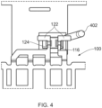
- Figure 4 illustrates the arrangement of Figure 3 connected to a semiconductor die consistent with the discussion above in relation to Figure 2 .
- a wire loop or hook 402 of a wire pull test equipment looped under the hooking tab 122 of the gate lead 124.
- Figure 5 illustrates a further example according to embodiments whereby the hooking tab 122 includes an extension portion 123.
- this extension portion By including this extension portion the pulling moment on the hooking tab 122 may be further increased when compared to the arrangement of Figure 2 , whilst ensuring that the hooking tab 122 and extension portion 123 do not extend outside the eventually moulded semiconductor device.
- the extension portion 123 should preferably be arranged such that when viewed from above as in Figure 2 , it points away from the centre of semiconductor die.
- Figure 5 illustrates the extension portion 123 arranged on the hooking tab 122 of the gate lead, following the above principles, the skilled person will appreciate that a similar extension portion could be included on the source lead.
- the first leads 112, 124 may form source connections to a source terminal on top side of the semiconductor die 106.
- the second leads 116 may form a gate connection to a gate terminal 118 also formed on the top side of the semiconductor die 106.
- the semiconductor die 106 may be a field effect transistor.
- FIG. 6 a matrix arrangement 600 of lead frame assemblies 100 according to embodiments as discussed above is illustrated.
- the matrix 600 is arranged as a 4 x 5 matrix, however the skilled will appreciate that any number of rows or columns may be included.
- the inset to Figure 6 illustrates an individual leadframe assembly 100 according to the above described arrangements and the matrix 600 illustrates the interconnected nature of matrix of individual leadframe assemblies.
- the hooking feature may be applied to one of more of a base clip, collector clip or emitter clip connections as appropriate.
- the semiconductor die is a bipolar junction transistor.
- the first leads 112 may form collector connections to a collector terminal 110 on the top side of a semiconductor die.
- the second lead 124 may form a base connection to a base terminal also formed on the top side of the semiconductor die 108.
Landscapes
- Lead Frames For Integrated Circuits (AREA)
Claims (10)
- Leadframe-Anordnung (100) für eine Halbleitervorrichtung, wobei die Leadframe-Anordnung Folgendes umfasst:eine Clip-Rahmenstruktur;wobei die Clip-Rahmenstruktur Folgendes umfasst:einen Chipanschlussabschnitt, der für den Kontakt mit einer oder mehreren Kontaktklemmen auf einer Oberseite eines Halbleiterchips konfiguriert und angeordnet ist,eine oder mehrere elektrische Leitungen (112, 116), die sich von dem Chipanschlussabschnitt an einem ersten Ende erstrecken,wobei der Chipanschlussabschnitt eine sich davon erstreckende Hakenlasche (122) umfasst, die dazu konfiguriert und angeordnet ist, mit einer Drahtschlinge eines Drahtzugprüfgeräts in Eingriff gebracht zu werden,dadurch gekennzeichnet, dass die Hakenlasche (122) derart angeordnet ist, dass sie sich orthogonal von dem Chipanschlussabschnitt erstreckt,wobei die Hakenlasche (122) mit dem Chipanschlussabschnitt einstückig ausgebildet ist.
- Leadframe-Anordnung nach Anspruch 1, wobei der Chipanschlussabschnitt im Wesentlichen langgestreckt ist und an einer Stelle, an der der Chipanschlussabschnitt für den Kontakt mit einer Klemme des Halbleiterchips angeordnet ist, einen sich nach unten erstreckenden Abschnitt umfasst.
- Leadframe-Anordnung nach Anspruch 2, wobei der sich nach unten erstreckende Abschnitt die Hakenlasche entsprechend der Höhe des sich nach unten erstreckenden Abschnitts anhebt.
- Leadframe-Anordnung nach einem der vorangehenden Ansprüche, wobei die Hakenlasche einen sich davon erstreckenden Verlängerungsabschnitt umfasst, der für den Eingriff mit einer Drahtschlinge eines Drahtzugprüfgeräts konfiguriert und angeordnet ist.
- Leadframe-Anordnung nach einem der Ansprüche 1 bis 4, wobei der Verlängerungsabschnitt mit der Hakenlasche einstückig ausgebildet ist.
- Leadframe-Anordnung nach einem der vorangehenden Ansprüche, wobei es sich bei dem Chipanschlussabschnitt um einen Gate-Anschluss an den Halbleiterchip handelt.
- Leadframe-Anordnung nach einem der Ansprüche 1 bis 3, wobei es sich bei dem Chipanschlussabschnitt um einen Source-Anschluss an den Halbleiterchip handelt.
- Leadframe-Anordnung nach einem der vorangehenden Ansprüche, ferner umfassend eine Dam-Bar, die sich orthogonal über die eine oder die mehreren elektrischen Leitungen erstreckt.
- Matrix von Leadframes, wobei eine Einheit der Matrix eine Leadframe-Anordnung nach einem der vorangehenden Ansprüche umfasst.
- Matrix von Leadframes nach Anspruch 9, wobei aneinander angrenzende Einheiten der Matrix durch jeweilige Dam-Bars jeder Leadframe-Anordnung verbunden sind.
Priority Applications (3)
| Application Number | Priority Date | Filing Date | Title |
|---|---|---|---|
| EP18212898.3A EP3671829B1 (de) | 2018-12-17 | 2018-12-17 | Leitungsrahmenanordnung für ein halbleiterbauelement |
| US16/715,385 US10714413B2 (en) | 2018-12-17 | 2019-12-16 | Leadframe assembly for a semiconductor device |
| CN201911291444.4A CN111326493B (zh) | 2018-12-17 | 2019-12-16 | 用于半导体装置的引线框架组件 |
Applications Claiming Priority (1)
| Application Number | Priority Date | Filing Date | Title |
|---|---|---|---|
| EP18212898.3A EP3671829B1 (de) | 2018-12-17 | 2018-12-17 | Leitungsrahmenanordnung für ein halbleiterbauelement |
Publications (2)
| Publication Number | Publication Date |
|---|---|
| EP3671829A1 EP3671829A1 (de) | 2020-06-24 |
| EP3671829B1 true EP3671829B1 (de) | 2023-09-27 |
Family
ID=64755125
Family Applications (1)
| Application Number | Title | Priority Date | Filing Date |
|---|---|---|---|
| EP18212898.3A Active EP3671829B1 (de) | 2018-12-17 | 2018-12-17 | Leitungsrahmenanordnung für ein halbleiterbauelement |
Country Status (3)
| Country | Link |
|---|---|
| US (1) | US10714413B2 (de) |
| EP (1) | EP3671829B1 (de) |
| CN (1) | CN111326493B (de) |
Family Cites Families (11)
| Publication number | Priority date | Publication date | Assignee | Title |
|---|---|---|---|---|
| US5110761A (en) * | 1988-09-09 | 1992-05-05 | Motorola, Inc. | Formed top contact for non-flat semiconductor devices |
| US4994412A (en) * | 1990-02-09 | 1991-02-19 | Motorola Inc. | Self-centering electrode for power devices |
| US6204074B1 (en) * | 1995-01-09 | 2001-03-20 | International Business Machines Corporation | Chip design process for wire bond and flip-chip package |
| JPH09274065A (ja) * | 1996-04-03 | 1997-10-21 | Sumitomo Electric Ind Ltd | 半導体装置 |
| US7683464B2 (en) * | 2005-09-13 | 2010-03-23 | Alpha And Omega Semiconductor Incorporated | Semiconductor package having dimpled plate interconnections |
| JP4705881B2 (ja) * | 2006-05-09 | 2011-06-22 | パナソニック株式会社 | リードフレーム及びそれを用いた半導体装置 |
| JP5220714B2 (ja) * | 2009-09-18 | 2013-06-26 | セイコーインスツル株式会社 | 樹脂封止型半導体装置及びその製造方法 |
| JP5823798B2 (ja) * | 2011-09-29 | 2015-11-25 | ルネサスエレクトロニクス株式会社 | 半導体装置 |
| JP6451117B2 (ja) * | 2014-04-01 | 2019-01-16 | 富士電機株式会社 | 半導体装置の製造方法および半導体装置 |
| EP2930747A1 (de) * | 2014-04-07 | 2015-10-14 | Nxp B.V. | Leitung zum Anschluss an eine Halbleitervorrichtung |
| US10825757B2 (en) * | 2016-12-19 | 2020-11-03 | Nexperia B.V. | Semiconductor device and method with clip arrangement in IC package |
-
2018
- 2018-12-17 EP EP18212898.3A patent/EP3671829B1/de active Active
-
2019
- 2019-12-16 US US16/715,385 patent/US10714413B2/en active Active
- 2019-12-16 CN CN201911291444.4A patent/CN111326493B/zh active Active
Also Published As
| Publication number | Publication date |
|---|---|
| US10714413B2 (en) | 2020-07-14 |
| US20200194354A1 (en) | 2020-06-18 |
| EP3671829A1 (de) | 2020-06-24 |
| CN111326493A (zh) | 2020-06-23 |
| CN111326493B (zh) | 2024-09-13 |
Similar Documents
| Publication | Publication Date | Title |
|---|---|---|
| US9812384B2 (en) | Semiconductor device having compliant and crack-arresting interconnect structure | |
| US20240258207A1 (en) | Lead frame assembly for a semiconductor device | |
| US8384206B2 (en) | Semiconductor package | |
| US9171766B2 (en) | Lead frame strips with support members | |
| KR101912949B1 (ko) | 볼 그리드 어레이 패키지용 테스트 소켓 | |
| US5574383A (en) | IC tester and measuring method | |
| US6854637B2 (en) | Wirebonding insulated wire | |
| EP3671829B1 (de) | Leitungsrahmenanordnung für ein halbleiterbauelement | |
| US6220102B1 (en) | Die-shear test fixture apparatus | |
| US20180261567A1 (en) | Window Clamp | |
| KR101302112B1 (ko) | 다접점 콘택트핀 및 이를 포함하는 반도체 패키지 테스트용 소켓 | |
| US9153518B2 (en) | Molded semiconductor package with pluggable lead | |
| US20090079042A1 (en) | Center Conductor to Integrated Circuit for High Frequency Applications | |
| JPH06132449A (ja) | 半導体装置 | |
| CN107919294B (zh) | 半导体器件制造方法和半导体器件 | |
| CN222233606U (zh) | 解封装引线框架治具和解封装测试设备 | |
| KR200151991Y1 (ko) | 반도체 패키지 테스트를 위한 리드 콘택용 전도성시트 | |
| JP2026513663A (ja) | 導電接続、パワー半導体モジュール、および導電接続を製造するための方法 | |
| US6163063A (en) | Semiconductor device | |
| JPH03283443A (ja) | 半導体装置の電気特性検査用ハンドラ装置 | |
| JPH09274065A (ja) | 半導体装置 | |
| JPH02167485A (ja) | 接続装置 | |
| JP2003177156A (ja) | 半導体装置の製造方法 | |
| JPH10208836A (ja) | Icソケット | |
| JP2003149288A (ja) | コンタクトシートを有する半導体検査装置 |
Legal Events
| Date | Code | Title | Description |
|---|---|---|---|
| PUAI | Public reference made under article 153(3) epc to a published international application that has entered the european phase |
Free format text: ORIGINAL CODE: 0009012 |
|
| STAA | Information on the status of an ep patent application or granted ep patent |
Free format text: STATUS: THE APPLICATION HAS BEEN PUBLISHED |
|
| AK | Designated contracting states |
Kind code of ref document: A1 Designated state(s): AL AT BE BG CH CY CZ DE DK EE ES FI FR GB GR HR HU IE IS IT LI LT LU LV MC MK MT NL NO PL PT RO RS SE SI SK SM TR |
|
| AX | Request for extension of the european patent |
Extension state: BA ME |
|
| STAA | Information on the status of an ep patent application or granted ep patent |
Free format text: STATUS: REQUEST FOR EXAMINATION WAS MADE |
|
| 17P | Request for examination filed |
Effective date: 20201224 |
|
| RBV | Designated contracting states (corrected) |
Designated state(s): AL AT BE BG CH CY CZ DE DK EE ES FI FR GB GR HR HU IE IS IT LI LT LU LV MC MK MT NL NO PL PT RO RS SE SI SK SM TR |
|
| STAA | Information on the status of an ep patent application or granted ep patent |
Free format text: STATUS: EXAMINATION IS IN PROGRESS |
|
| 17Q | First examination report despatched |
Effective date: 20210423 |
|
| GRAP | Despatch of communication of intention to grant a patent |
Free format text: ORIGINAL CODE: EPIDOSNIGR1 |
|
| STAA | Information on the status of an ep patent application or granted ep patent |
Free format text: STATUS: GRANT OF PATENT IS INTENDED |
|
| INTG | Intention to grant announced |
Effective date: 20230509 |
|
| GRAS | Grant fee paid |
Free format text: ORIGINAL CODE: EPIDOSNIGR3 |
|
| GRAA | (expected) grant |
Free format text: ORIGINAL CODE: 0009210 |
|
| STAA | Information on the status of an ep patent application or granted ep patent |
Free format text: STATUS: THE PATENT HAS BEEN GRANTED |
|
| AK | Designated contracting states |
Kind code of ref document: B1 Designated state(s): AL AT BE BG CH CY CZ DE DK EE ES FI FR GB GR HR HU IE IS IT LI LT LU LV MC MK MT NL NO PL PT RO RS SE SI SK SM TR |
|
| REG | Reference to a national code |
Ref country code: GB Ref legal event code: FG4D |
|
| REG | Reference to a national code |
Ref country code: CH Ref legal event code: EP |
|
| REG | Reference to a national code |
Ref country code: DE Ref legal event code: R096 Ref document number: 602018058198 Country of ref document: DE |
|
| REG | Reference to a national code |
Ref country code: IE Ref legal event code: FG4D |
|
| REG | Reference to a national code |
Ref country code: LT Ref legal event code: MG9D |
|
| PG25 | Lapsed in a contracting state [announced via postgrant information from national office to epo] |
Ref country code: GR Free format text: LAPSE BECAUSE OF FAILURE TO SUBMIT A TRANSLATION OF THE DESCRIPTION OR TO PAY THE FEE WITHIN THE PRESCRIBED TIME-LIMIT Effective date: 20231228 |
|
| PG25 | Lapsed in a contracting state [announced via postgrant information from national office to epo] |
Ref country code: SE Free format text: LAPSE BECAUSE OF FAILURE TO SUBMIT A TRANSLATION OF THE DESCRIPTION OR TO PAY THE FEE WITHIN THE PRESCRIBED TIME-LIMIT Effective date: 20230927 Ref country code: RS Free format text: LAPSE BECAUSE OF FAILURE TO SUBMIT A TRANSLATION OF THE DESCRIPTION OR TO PAY THE FEE WITHIN THE PRESCRIBED TIME-LIMIT Effective date: 20230927 Ref country code: NO Free format text: LAPSE BECAUSE OF FAILURE TO SUBMIT A TRANSLATION OF THE DESCRIPTION OR TO PAY THE FEE WITHIN THE PRESCRIBED TIME-LIMIT Effective date: 20231227 Ref country code: LV Free format text: LAPSE BECAUSE OF FAILURE TO SUBMIT A TRANSLATION OF THE DESCRIPTION OR TO PAY THE FEE WITHIN THE PRESCRIBED TIME-LIMIT Effective date: 20230927 Ref country code: LT Free format text: LAPSE BECAUSE OF FAILURE TO SUBMIT A TRANSLATION OF THE DESCRIPTION OR TO PAY THE FEE WITHIN THE PRESCRIBED TIME-LIMIT Effective date: 20230927 Ref country code: HR Free format text: LAPSE BECAUSE OF FAILURE TO SUBMIT A TRANSLATION OF THE DESCRIPTION OR TO PAY THE FEE WITHIN THE PRESCRIBED TIME-LIMIT Effective date: 20230927 Ref country code: GR Free format text: LAPSE BECAUSE OF FAILURE TO SUBMIT A TRANSLATION OF THE DESCRIPTION OR TO PAY THE FEE WITHIN THE PRESCRIBED TIME-LIMIT Effective date: 20231228 Ref country code: FI Free format text: LAPSE BECAUSE OF FAILURE TO SUBMIT A TRANSLATION OF THE DESCRIPTION OR TO PAY THE FEE WITHIN THE PRESCRIBED TIME-LIMIT Effective date: 20230927 |
|
| REG | Reference to a national code |
Ref country code: NL Ref legal event code: MP Effective date: 20230927 |
|
| REG | Reference to a national code |
Ref country code: AT Ref legal event code: MK05 Ref document number: 1616293 Country of ref document: AT Kind code of ref document: T Effective date: 20230927 |
|
| PG25 | Lapsed in a contracting state [announced via postgrant information from national office to epo] |
Ref country code: NL Free format text: LAPSE BECAUSE OF FAILURE TO SUBMIT A TRANSLATION OF THE DESCRIPTION OR TO PAY THE FEE WITHIN THE PRESCRIBED TIME-LIMIT Effective date: 20230927 |
|
| PG25 | Lapsed in a contracting state [announced via postgrant information from national office to epo] |
Ref country code: IS Free format text: LAPSE BECAUSE OF FAILURE TO SUBMIT A TRANSLATION OF THE DESCRIPTION OR TO PAY THE FEE WITHIN THE PRESCRIBED TIME-LIMIT Effective date: 20240127 |
|
| PG25 | Lapsed in a contracting state [announced via postgrant information from national office to epo] |
Ref country code: AT Free format text: LAPSE BECAUSE OF FAILURE TO SUBMIT A TRANSLATION OF THE DESCRIPTION OR TO PAY THE FEE WITHIN THE PRESCRIBED TIME-LIMIT Effective date: 20230927 |
|
| PG25 | Lapsed in a contracting state [announced via postgrant information from national office to epo] |
Ref country code: ES Free format text: LAPSE BECAUSE OF FAILURE TO SUBMIT A TRANSLATION OF THE DESCRIPTION OR TO PAY THE FEE WITHIN THE PRESCRIBED TIME-LIMIT Effective date: 20230927 |
|
| PG25 | Lapsed in a contracting state [announced via postgrant information from national office to epo] |
Ref country code: SM Free format text: LAPSE BECAUSE OF FAILURE TO SUBMIT A TRANSLATION OF THE DESCRIPTION OR TO PAY THE FEE WITHIN THE PRESCRIBED TIME-LIMIT Effective date: 20230927 Ref country code: RO Free format text: LAPSE BECAUSE OF FAILURE TO SUBMIT A TRANSLATION OF THE DESCRIPTION OR TO PAY THE FEE WITHIN THE PRESCRIBED TIME-LIMIT Effective date: 20230927 Ref country code: IS Free format text: LAPSE BECAUSE OF FAILURE TO SUBMIT A TRANSLATION OF THE DESCRIPTION OR TO PAY THE FEE WITHIN THE PRESCRIBED TIME-LIMIT Effective date: 20240127 Ref country code: ES Free format text: LAPSE BECAUSE OF FAILURE TO SUBMIT A TRANSLATION OF THE DESCRIPTION OR TO PAY THE FEE WITHIN THE PRESCRIBED TIME-LIMIT Effective date: 20230927 Ref country code: EE Free format text: LAPSE BECAUSE OF FAILURE TO SUBMIT A TRANSLATION OF THE DESCRIPTION OR TO PAY THE FEE WITHIN THE PRESCRIBED TIME-LIMIT Effective date: 20230927 Ref country code: CZ Free format text: LAPSE BECAUSE OF FAILURE TO SUBMIT A TRANSLATION OF THE DESCRIPTION OR TO PAY THE FEE WITHIN THE PRESCRIBED TIME-LIMIT Effective date: 20230927 Ref country code: AT Free format text: LAPSE BECAUSE OF FAILURE TO SUBMIT A TRANSLATION OF THE DESCRIPTION OR TO PAY THE FEE WITHIN THE PRESCRIBED TIME-LIMIT Effective date: 20230927 Ref country code: PT Free format text: LAPSE BECAUSE OF FAILURE TO SUBMIT A TRANSLATION OF THE DESCRIPTION OR TO PAY THE FEE WITHIN THE PRESCRIBED TIME-LIMIT Effective date: 20240129 Ref country code: SK Free format text: LAPSE BECAUSE OF FAILURE TO SUBMIT A TRANSLATION OF THE DESCRIPTION OR TO PAY THE FEE WITHIN THE PRESCRIBED TIME-LIMIT Effective date: 20230927 |
|
| PG25 | Lapsed in a contracting state [announced via postgrant information from national office to epo] |
Ref country code: PL Free format text: LAPSE BECAUSE OF FAILURE TO SUBMIT A TRANSLATION OF THE DESCRIPTION OR TO PAY THE FEE WITHIN THE PRESCRIBED TIME-LIMIT Effective date: 20230927 Ref country code: IT Free format text: LAPSE BECAUSE OF FAILURE TO SUBMIT A TRANSLATION OF THE DESCRIPTION OR TO PAY THE FEE WITHIN THE PRESCRIBED TIME-LIMIT Effective date: 20230927 |
|
| REG | Reference to a national code |
Ref country code: DE Ref legal event code: R097 Ref document number: 602018058198 Country of ref document: DE |
|
| PG25 | Lapsed in a contracting state [announced via postgrant information from national office to epo] |
Ref country code: DK Free format text: LAPSE BECAUSE OF FAILURE TO SUBMIT A TRANSLATION OF THE DESCRIPTION OR TO PAY THE FEE WITHIN THE PRESCRIBED TIME-LIMIT Effective date: 20230927 |
|
| PG25 | Lapsed in a contracting state [announced via postgrant information from national office to epo] |
Ref country code: DK Free format text: LAPSE BECAUSE OF FAILURE TO SUBMIT A TRANSLATION OF THE DESCRIPTION OR TO PAY THE FEE WITHIN THE PRESCRIBED TIME-LIMIT Effective date: 20230927 |
|
| REG | Reference to a national code |
Ref country code: CH Ref legal event code: PL |
|
| PLBE | No opposition filed within time limit |
Free format text: ORIGINAL CODE: 0009261 |
|
| STAA | Information on the status of an ep patent application or granted ep patent |
Free format text: STATUS: NO OPPOSITION FILED WITHIN TIME LIMIT |
|
| PG25 | Lapsed in a contracting state [announced via postgrant information from national office to epo] |
Ref country code: LU Free format text: LAPSE BECAUSE OF NON-PAYMENT OF DUE FEES Effective date: 20231217 |
|
| PG25 | Lapsed in a contracting state [announced via postgrant information from national office to epo] |
Ref country code: MC Free format text: LAPSE BECAUSE OF FAILURE TO SUBMIT A TRANSLATION OF THE DESCRIPTION OR TO PAY THE FEE WITHIN THE PRESCRIBED TIME-LIMIT Effective date: 20230927 |
|
| GBPC | Gb: european patent ceased through non-payment of renewal fee |
Effective date: 20231227 |
|
| REG | Reference to a national code |
Ref country code: BE Ref legal event code: MM Effective date: 20231231 |
|
| PG25 | Lapsed in a contracting state [announced via postgrant information from national office to epo] |
Ref country code: MC Free format text: LAPSE BECAUSE OF FAILURE TO SUBMIT A TRANSLATION OF THE DESCRIPTION OR TO PAY THE FEE WITHIN THE PRESCRIBED TIME-LIMIT Effective date: 20230927 Ref country code: LU Free format text: LAPSE BECAUSE OF NON-PAYMENT OF DUE FEES Effective date: 20231217 |
|
| 26N | No opposition filed |
Effective date: 20240628 |
|
| REG | Reference to a national code |
Ref country code: IE Ref legal event code: MM4A |
|
| PG25 | Lapsed in a contracting state [announced via postgrant information from national office to epo] |
Ref country code: IE Free format text: LAPSE BECAUSE OF NON-PAYMENT OF DUE FEES Effective date: 20231217 |
|
| PG25 | Lapsed in a contracting state [announced via postgrant information from national office to epo] |
Ref country code: GB Free format text: LAPSE BECAUSE OF NON-PAYMENT OF DUE FEES Effective date: 20231227 |
|
| PG25 | Lapsed in a contracting state [announced via postgrant information from national office to epo] |
Ref country code: BE Free format text: LAPSE BECAUSE OF NON-PAYMENT OF DUE FEES Effective date: 20231231 |
|
| PG25 | Lapsed in a contracting state [announced via postgrant information from national office to epo] |
Ref country code: FR Free format text: LAPSE BECAUSE OF NON-PAYMENT OF DUE FEES Effective date: 20231231 |
|
| PG25 | Lapsed in a contracting state [announced via postgrant information from national office to epo] |
Ref country code: CH Free format text: LAPSE BECAUSE OF NON-PAYMENT OF DUE FEES Effective date: 20231231 |
|
| PG25 | Lapsed in a contracting state [announced via postgrant information from national office to epo] |
Ref country code: SI Free format text: LAPSE BECAUSE OF FAILURE TO SUBMIT A TRANSLATION OF THE DESCRIPTION OR TO PAY THE FEE WITHIN THE PRESCRIBED TIME-LIMIT Effective date: 20230927 |
|
| PG25 | Lapsed in a contracting state [announced via postgrant information from national office to epo] |
Ref country code: SI Free format text: LAPSE BECAUSE OF FAILURE TO SUBMIT A TRANSLATION OF THE DESCRIPTION OR TO PAY THE FEE WITHIN THE PRESCRIBED TIME-LIMIT Effective date: 20230927 Ref country code: IE Free format text: LAPSE BECAUSE OF NON-PAYMENT OF DUE FEES Effective date: 20231217 Ref country code: GB Free format text: LAPSE BECAUSE OF NON-PAYMENT OF DUE FEES Effective date: 20231227 Ref country code: FR Free format text: LAPSE BECAUSE OF NON-PAYMENT OF DUE FEES Effective date: 20231231 Ref country code: CH Free format text: LAPSE BECAUSE OF NON-PAYMENT OF DUE FEES Effective date: 20231231 Ref country code: BE Free format text: LAPSE BECAUSE OF NON-PAYMENT OF DUE FEES Effective date: 20231231 |
|
| PG25 | Lapsed in a contracting state [announced via postgrant information from national office to epo] |
Ref country code: BG Free format text: LAPSE BECAUSE OF FAILURE TO SUBMIT A TRANSLATION OF THE DESCRIPTION OR TO PAY THE FEE WITHIN THE PRESCRIBED TIME-LIMIT Effective date: 20230927 |
|
| PG25 | Lapsed in a contracting state [announced via postgrant information from national office to epo] |
Ref country code: BG Free format text: LAPSE BECAUSE OF FAILURE TO SUBMIT A TRANSLATION OF THE DESCRIPTION OR TO PAY THE FEE WITHIN THE PRESCRIBED TIME-LIMIT Effective date: 20230927 |
|
| PG25 | Lapsed in a contracting state [announced via postgrant information from national office to epo] |
Ref country code: CY Free format text: LAPSE BECAUSE OF FAILURE TO SUBMIT A TRANSLATION OF THE DESCRIPTION OR TO PAY THE FEE WITHIN THE PRESCRIBED TIME-LIMIT; INVALID AB INITIO Effective date: 20181217 |
|
| PG25 | Lapsed in a contracting state [announced via postgrant information from national office to epo] |
Ref country code: HU Free format text: LAPSE BECAUSE OF FAILURE TO SUBMIT A TRANSLATION OF THE DESCRIPTION OR TO PAY THE FEE WITHIN THE PRESCRIBED TIME-LIMIT; INVALID AB INITIO Effective date: 20181217 |
|
| REG | Reference to a national code |
Ref country code: DE Ref legal event code: R079 Ref document number: 602018058198 Country of ref document: DE Free format text: PREVIOUS MAIN CLASS: H01L0023495000 Ipc: H10W0070400000 |
|
| PG25 | Lapsed in a contracting state [announced via postgrant information from national office to epo] |
Ref country code: TR Free format text: LAPSE BECAUSE OF FAILURE TO SUBMIT A TRANSLATION OF THE DESCRIPTION OR TO PAY THE FEE WITHIN THE PRESCRIBED TIME-LIMIT Effective date: 20230927 |
|
| PGFP | Annual fee paid to national office [announced via postgrant information from national office to epo] |
Ref country code: DE Payment date: 20251229 Year of fee payment: 8 |