EP3671836B1 - 3d schaltung mit einer mesa-isolation für den grundplattenbereich - Google Patents
3d schaltung mit einer mesa-isolation für den grundplattenbereich Download PDFInfo
- Publication number
- EP3671836B1 EP3671836B1 EP19213818.8A EP19213818A EP3671836B1 EP 3671836 B1 EP3671836 B1 EP 3671836B1 EP 19213818 A EP19213818 A EP 19213818A EP 3671836 B1 EP3671836 B1 EP 3671836B1
- Authority
- EP
- European Patent Office
- Prior art keywords
- layer
- ground plane
- semiconductor
- island
- plane layer
- Prior art date
- Legal status (The legal status is an assumption and is not a legal conclusion. Google has not performed a legal analysis and makes no representation as to the accuracy of the status listed.)
- Active
Links
Images



Classifications
-
- H—ELECTRICITY
- H10—SEMICONDUCTOR DEVICES; ELECTRIC SOLID-STATE DEVICES NOT OTHERWISE PROVIDED FOR
- H10D—INORGANIC ELECTRIC SEMICONDUCTOR DEVICES
- H10D87/00—Integrated devices comprising both bulk components and either SOI or SOS components on the same substrate
-
- H—ELECTRICITY
- H10—SEMICONDUCTOR DEVICES; ELECTRIC SOLID-STATE DEVICES NOT OTHERWISE PROVIDED FOR
- H10D—INORGANIC ELECTRIC SEMICONDUCTOR DEVICES
- H10D84/00—Integrated devices formed in or on semiconductor substrates that comprise only semiconducting layers, e.g. on Si wafers or on GaAs-on-Si wafers
- H10D84/01—Manufacture or treatment
- H10D84/0123—Integrating together multiple components covered by H10D12/00 or H10D30/00, e.g. integrating multiple IGBTs
- H10D84/0126—Integrating together multiple components covered by H10D12/00 or H10D30/00, e.g. integrating multiple IGBTs the components including insulated gates, e.g. IGFETs
- H10D84/0135—Manufacturing their gate conductors
-
- H—ELECTRICITY
- H10—SEMICONDUCTOR DEVICES; ELECTRIC SOLID-STATE DEVICES NOT OTHERWISE PROVIDED FOR
- H10D—INORGANIC ELECTRIC SEMICONDUCTOR DEVICES
- H10D84/00—Integrated devices formed in or on semiconductor substrates that comprise only semiconducting layers, e.g. on Si wafers or on GaAs-on-Si wafers
- H10D84/01—Manufacture or treatment
- H10D84/02—Manufacture or treatment characterised by using material-based technologies
- H10D84/03—Manufacture or treatment characterised by using material-based technologies using Group IV technology, e.g. silicon technology or silicon-carbide [SiC] technology
- H10D84/038—Manufacture or treatment characterised by using material-based technologies using Group IV technology, e.g. silicon technology or silicon-carbide [SiC] technology using silicon technology, e.g. SiGe
-
- H—ELECTRICITY
- H10—SEMICONDUCTOR DEVICES; ELECTRIC SOLID-STATE DEVICES NOT OTHERWISE PROVIDED FOR
- H10D—INORGANIC ELECTRIC SEMICONDUCTOR DEVICES
- H10D86/00—Integrated devices formed in or on insulating or conducting substrates, e.g. formed in silicon-on-insulator [SOI] substrates or on stainless steel or glass substrates
- H10D86/01—Manufacture or treatment
-
- H—ELECTRICITY
- H10—SEMICONDUCTOR DEVICES; ELECTRIC SOLID-STATE DEVICES NOT OTHERWISE PROVIDED FOR
- H10D—INORGANIC ELECTRIC SEMICONDUCTOR DEVICES
- H10D88/00—Three-dimensional [3D] integrated devices
- H10D88/01—Manufacture or treatment
-
- H—ELECTRICITY
- H10—SEMICONDUCTOR DEVICES; ELECTRIC SOLID-STATE DEVICES NOT OTHERWISE PROVIDED FOR
- H10P—GENERIC PROCESSES OR APPARATUS FOR THE MANUFACTURE OR TREATMENT OF DEVICES COVERED BY CLASS H10
- H10P14/00—Formation of materials, e.g. in the shape of layers or pillars
- H10P14/20—Formation of materials, e.g. in the shape of layers or pillars of semiconductor materials
- H10P14/38—Formation of materials, e.g. in the shape of layers or pillars of semiconductor materials characterised by treatments done after the formation of the materials
- H10P14/3802—Crystallisation or recrystallisation of non-monocrystalline semiconductor materials, e.g. regrowth
-
- H—ELECTRICITY
- H10—SEMICONDUCTOR DEVICES; ELECTRIC SOLID-STATE DEVICES NOT OTHERWISE PROVIDED FOR
- H10P—GENERIC PROCESSES OR APPARATUS FOR THE MANUFACTURE OR TREATMENT OF DEVICES COVERED BY CLASS H10
- H10P14/00—Formation of materials, e.g. in the shape of layers or pillars
- H10P14/40—Formation of materials, e.g. in the shape of layers or pillars of conductive or resistive materials
- H10P14/412—Deposition of metallic or metal-silicide materials
- H10P14/414—Deposition of metallic or metal-silicide materials of metal-silicide materials
-
- H—ELECTRICITY
- H10—SEMICONDUCTOR DEVICES; ELECTRIC SOLID-STATE DEVICES NOT OTHERWISE PROVIDED FOR
- H10P—GENERIC PROCESSES OR APPARATUS FOR THE MANUFACTURE OR TREATMENT OF DEVICES COVERED BY CLASS H10
- H10P14/00—Formation of materials, e.g. in the shape of layers or pillars
- H10P14/60—Formation of materials, e.g. in the shape of layers or pillars of insulating materials
- H10P14/69—Inorganic materials
- H10P14/692—Inorganic materials composed of oxides, glassy oxides or oxide-based glasses
- H10P14/6921—Inorganic materials composed of oxides, glassy oxides or oxide-based glasses containing silicon
- H10P14/69215—Inorganic materials composed of oxides, glassy oxides or oxide-based glasses containing silicon the material being a silicon oxide, e.g. SiO2
-
- H—ELECTRICITY
- H10—SEMICONDUCTOR DEVICES; ELECTRIC SOLID-STATE DEVICES NOT OTHERWISE PROVIDED FOR
- H10P—GENERIC PROCESSES OR APPARATUS FOR THE MANUFACTURE OR TREATMENT OF DEVICES COVERED BY CLASS H10
- H10P14/00—Formation of materials, e.g. in the shape of layers or pillars
- H10P14/60—Formation of materials, e.g. in the shape of layers or pillars of insulating materials
- H10P14/69—Inorganic materials
- H10P14/692—Inorganic materials composed of oxides, glassy oxides or oxide-based glasses
- H10P14/6921—Inorganic materials composed of oxides, glassy oxides or oxide-based glasses containing silicon
- H10P14/6922—Inorganic materials composed of oxides, glassy oxides or oxide-based glasses containing silicon the material containing Si, O and at least one of H, N, C, F or other non-metal elements, e.g. SiOC, SiOC:H or SiONC
-
- H—ELECTRICITY
- H10—SEMICONDUCTOR DEVICES; ELECTRIC SOLID-STATE DEVICES NOT OTHERWISE PROVIDED FOR
- H10P—GENERIC PROCESSES OR APPARATUS FOR THE MANUFACTURE OR TREATMENT OF DEVICES COVERED BY CLASS H10
- H10P30/00—Ion implantation into wafers, substrates or parts of devices
- H10P30/20—Ion implantation into wafers, substrates or parts of devices into semiconductor materials, e.g. for doping
- H10P30/202—Ion implantation into wafers, substrates or parts of devices into semiconductor materials, e.g. for doping characterised by the semiconductor materials
- H10P30/204—Ion implantation into wafers, substrates or parts of devices into semiconductor materials, e.g. for doping characterised by the semiconductor materials into Group IV semiconductors
-
- H—ELECTRICITY
- H10—SEMICONDUCTOR DEVICES; ELECTRIC SOLID-STATE DEVICES NOT OTHERWISE PROVIDED FOR
- H10P—GENERIC PROCESSES OR APPARATUS FOR THE MANUFACTURE OR TREATMENT OF DEVICES COVERED BY CLASS H10
- H10P30/00—Ion implantation into wafers, substrates or parts of devices
- H10P30/20—Ion implantation into wafers, substrates or parts of devices into semiconductor materials, e.g. for doping
- H10P30/21—Ion implantation into wafers, substrates or parts of devices into semiconductor materials, e.g. for doping of electrically active species
-
- H—ELECTRICITY
- H10—SEMICONDUCTOR DEVICES; ELECTRIC SOLID-STATE DEVICES NOT OTHERWISE PROVIDED FOR
- H10P—GENERIC PROCESSES OR APPARATUS FOR THE MANUFACTURE OR TREATMENT OF DEVICES COVERED BY CLASS H10
- H10P30/00—Ion implantation into wafers, substrates or parts of devices
- H10P30/20—Ion implantation into wafers, substrates or parts of devices into semiconductor materials, e.g. for doping
- H10P30/28—Ion implantation into wafers, substrates or parts of devices into semiconductor materials, e.g. for doping characterised by an annealing step, e.g. for activation of dopants
-
- H—ELECTRICITY
- H10—SEMICONDUCTOR DEVICES; ELECTRIC SOLID-STATE DEVICES NOT OTHERWISE PROVIDED FOR
- H10P—GENERIC PROCESSES OR APPARATUS FOR THE MANUFACTURE OR TREATMENT OF DEVICES COVERED BY CLASS H10
- H10P50/00—Etching of wafers, substrates or parts of devices
- H10P50/20—Dry etching; Plasma etching; Reactive-ion etching
- H10P50/28—Dry etching; Plasma etching; Reactive-ion etching of insulating materials
- H10P50/282—Dry etching; Plasma etching; Reactive-ion etching of insulating materials of inorganic materials
- H10P50/283—Dry etching; Plasma etching; Reactive-ion etching of insulating materials of inorganic materials by chemical means
-
- H—ELECTRICITY
- H10—SEMICONDUCTOR DEVICES; ELECTRIC SOLID-STATE DEVICES NOT OTHERWISE PROVIDED FOR
- H10P—GENERIC PROCESSES OR APPARATUS FOR THE MANUFACTURE OR TREATMENT OF DEVICES COVERED BY CLASS H10
- H10P50/00—Etching of wafers, substrates or parts of devices
- H10P50/60—Wet etching
- H10P50/64—Wet etching of semiconductor materials
- H10P50/642—Chemical etching
-
- H—ELECTRICITY
- H10—SEMICONDUCTOR DEVICES; ELECTRIC SOLID-STATE DEVICES NOT OTHERWISE PROVIDED FOR
- H10P—GENERIC PROCESSES OR APPARATUS FOR THE MANUFACTURE OR TREATMENT OF DEVICES COVERED BY CLASS H10
- H10P90/00—Preparation of wafers not covered by a single main group of this subclass, e.g. wafer reinforcement
- H10P90/19—Preparing inhomogeneous wafers
- H10P90/1904—Preparing vertically inhomogeneous wafers
- H10P90/1906—Preparing SOI wafers
- H10P90/1914—Preparing SOI wafers using bonding
- H10P90/1916—Preparing SOI wafers using bonding with separation or delamination along an ion implanted layer, e.g. Smart-cut
-
- H—ELECTRICITY
- H10—SEMICONDUCTOR DEVICES; ELECTRIC SOLID-STATE DEVICES NOT OTHERWISE PROVIDED FOR
- H10P—GENERIC PROCESSES OR APPARATUS FOR THE MANUFACTURE OR TREATMENT OF DEVICES COVERED BY CLASS H10
- H10P95/00—Generic processes or apparatus for manufacture or treatments not covered by the other groups of this subclass
- H10P95/90—Thermal treatments, e.g. annealing or sintering
-
- H—ELECTRICITY
- H10—SEMICONDUCTOR DEVICES; ELECTRIC SOLID-STATE DEVICES NOT OTHERWISE PROVIDED FOR
- H10W—GENERIC PACKAGES, INTERCONNECTIONS, CONNECTORS OR OTHER CONSTRUCTIONAL DETAILS OF DEVICES COVERED BY CLASS H10
- H10W10/00—Isolation regions in semiconductor bodies between components of integrated devices
- H10W10/10—Isolation regions comprising dielectric materials
- H10W10/181—Semiconductor-on-insulator [SOI] isolation regions, e.g. buried oxide regions of SOI wafers
-
- H—ELECTRICITY
- H10—SEMICONDUCTOR DEVICES; ELECTRIC SOLID-STATE DEVICES NOT OTHERWISE PROVIDED FOR
- H10W—GENERIC PACKAGES, INTERCONNECTIONS, CONNECTORS OR OTHER CONSTRUCTIONAL DETAILS OF DEVICES COVERED BY CLASS H10
- H10W20/00—Interconnections in chips, wafers or substrates
- H10W20/01—Manufacture or treatment
- H10W20/031—Manufacture or treatment of conductive parts of the interconnections
- H10W20/0698—Local interconnections
-
- H—ELECTRICITY
- H10—SEMICONDUCTOR DEVICES; ELECTRIC SOLID-STATE DEVICES NOT OTHERWISE PROVIDED FOR
- H10P—GENERIC PROCESSES OR APPARATUS FOR THE MANUFACTURE OR TREATMENT OF DEVICES COVERED BY CLASS H10
- H10P14/00—Formation of materials, e.g. in the shape of layers or pillars
- H10P14/60—Formation of materials, e.g. in the shape of layers or pillars of insulating materials
- H10P14/66—Formation of materials, e.g. in the shape of layers or pillars of insulating materials characterised by the type of materials
- H10P14/662—Laminate layers, e.g. stacks of alternating high-k metal oxides
-
- H—ELECTRICITY
- H10—SEMICONDUCTOR DEVICES; ELECTRIC SOLID-STATE DEVICES NOT OTHERWISE PROVIDED FOR
- H10P—GENERIC PROCESSES OR APPARATUS FOR THE MANUFACTURE OR TREATMENT OF DEVICES COVERED BY CLASS H10
- H10P14/00—Formation of materials, e.g. in the shape of layers or pillars
- H10P14/60—Formation of materials, e.g. in the shape of layers or pillars of insulating materials
- H10P14/69—Inorganic materials
- H10P14/692—Inorganic materials composed of oxides, glassy oxides or oxide-based glasses
- H10P14/6938—Inorganic materials composed of oxides, glassy oxides or oxide-based glasses the material containing at least one metal element, e.g. metal oxides, metal oxynitrides or metal oxycarbides
- H10P14/6939—Inorganic materials composed of oxides, glassy oxides or oxide-based glasses the material containing at least one metal element, e.g. metal oxides, metal oxynitrides or metal oxycarbides characterised by the metal
- H10P14/69392—Inorganic materials composed of oxides, glassy oxides or oxide-based glasses the material containing at least one metal element, e.g. metal oxides, metal oxynitrides or metal oxycarbides characterised by the metal the material containing hafnium, e.g. HfO2
-
- H—ELECTRICITY
- H10—SEMICONDUCTOR DEVICES; ELECTRIC SOLID-STATE DEVICES NOT OTHERWISE PROVIDED FOR
- H10P—GENERIC PROCESSES OR APPARATUS FOR THE MANUFACTURE OR TREATMENT OF DEVICES COVERED BY CLASS H10
- H10P14/00—Formation of materials, e.g. in the shape of layers or pillars
- H10P14/60—Formation of materials, e.g. in the shape of layers or pillars of insulating materials
- H10P14/69—Inorganic materials
- H10P14/694—Inorganic materials composed of nitrides
- H10P14/6943—Inorganic materials composed of nitrides containing silicon
- H10P14/69433—Inorganic materials composed of nitrides containing silicon the material being a silicon nitride not containing oxygen, e.g. SixNy or SixByNz
Definitions
- the present application concerns the field of integrated circuits equipped with electronic components distributed over several levels, in particular superimposed transistors. Such devices are generally referred to as “3D” circuits.
- one solution consists of distributing the transistors over several superimposed levels of semiconductor layers.
- Such 3-dimensional or “3D” integrated circuits thus typically comprise at least two semiconductor layers arranged one above the other and separated from each other by at least one insulating layer.
- ground plane layer In this type of device, it is known to integrate a layer of doped conductive or semiconductor material called a "ground plane” or “rear gate” layer, placed between the two superimposed semiconductor layers. Such a layer located under a higher level semiconductor layer is generally separated from this semiconductor layer via an insulating layer.
- This insulating layer is designed, in terms of material and thickness, so as to be able to implement electrostatic coupling between the ground plane layer and the upper level semiconductor layer.
- the ground plane layer can make it possible in particular to control the threshold voltage of a transistor whose channel region extends into the upper level semiconductor layer and which is located above this ground plane layer. massive.
- the ground plane layer can itself be etched in one or more distinct regions during the process of producing such a circuit.
- STI shallow tench isolation
- a trench is typically formed in a semiconductor layer and one or more dielectric materials such as silicon dioxide are deposited to fill the trench.
- the excess dielectric is then eliminated using at least one chemical-mechanical planarization (CMP) step.
- CMP chemical-mechanical planarization
- the production of STI type insulating zones may also require one or more oxide densification steps at high temperature.
- the ground plane layer is made of semiconductor material
- siliciding is carried out before carrying out the insulation, which can in particular make it possible to silicidate over a larger surface area and to produce contacts of improved quality and in particular of reduced resistance.
- an opening is formed in said insulating layer revealing a region of said first portion, at least one zone of metal and semiconductor compound being produced at said region of said first portion.
- the insulating layer can be provided with a thickness so that following said etchings at the end of step c), and prior to the formation of zones of metal compound and semiconductor, said first portion is revealed in a zone which extends around said island and is not located opposite said island.
- the conductive pads produced it is possible to provide at least one given conductive pad formed so as to pass through said space filled by said insulating material, said given conductive pad being connected to the first level N 1 of components.
- the insulating layer separating the ground plane layer from the second semiconductor layer can be formed from a stack of layers of different dielectric materials. This can make it possible to produce an insulating layer that is more resistant to etching.
- the insulating layer is made of silicon oxide
- the composition of the insulating layer is made more resistant to etching in order in particular to be able to preserve a thickness of this layer when doping is carried out to make junctions in the semiconductor island and allow thus to protect the ground plane layer during this doping.
- the method may comprise, prior to said assembly, a step of doping the ground plane layer , the ground plane layer being preferably doped according to a dopant concentration equal to or greater than 1 e 20 at/cm 3 .
- This structure comprises a first level N 1 of electronic components represented schematically by a broken line outline.
- This level N 1 is typically produced from a substrate comprising a first superficial semiconductor layer, for example made of silicon, in which one or more electronic components such as photo-sites and/or photodiodes and/or transistors are at least partially formed.
- a substrate comprising a first superficial semiconductor layer, for example made of silicon, in which one or more electronic components such as photo-sites and/or photodiodes and/or transistors are at least partially formed.
- the components of the first level N 1 are transistors T 11 and T 12 , in particular of the MOS type (MOS for “Metal Oxide Semi-conductor”) and have respective channel regions which extend in the first semi-conductor layer.
- conductive 11 One or more conductive connection zones 21 belonging to the first level N 1 can also be formed at this stage above the transistors T 11 , T 12 and are connected to the latter.
- the conductive connection zones 21 are typically made of metal, for example tungsten, and are arranged in at least one insulating layer 20 placed on the transistors.
- a stack of layers is typically produced by transfer to this first level N 1 .
- the stack is equipped in particular with a so-called “ground plane” layer 34 intended to carry out a polarization below at least one transistor of a second level N 2 and to be able in particular to modulate the threshold voltage of this transistor.
- the ground plane layer 34 firstly extends typically in full plate, in other words continuously between the first level N 1 and the second level N 2 .
- the ground plane layer 34 may be a conductive material such as a metal or an alloy of metal and semiconductor or advantageously be a doped semiconductor material or intended to be doped.
- layer 34 is provided based on doped polysilicon or intended to be doped.
- a ground plane layer 34 doped during its formation ( in situ doping) for example by deposition of semiconductor in amorphous or polycrystalline form can be produced.
- Annealing can activate the dopants or increase the activation level and make the semiconductor material polycrystalline in the case where it has been deposited in amorphous form.
- doping can be carried out by implantation of this layer 34, which can make it possible to achieve a high doping level.
- a thin ground plane layer 34 is used, for example less than 100 nm.
- the ground plane layer 34 when it is based on a doped semiconductor material, is preferably provided with a high concentration of dopants advantageously higher than that provided for areas of the second semiconductor layer 36 intended to form source and drain or channel access regions of a transistor of the second level N 2 .
- the dopant concentration is chosen of the order of 1 e 20 at/cm 3 or greater in the ground plane layer 34.
- an insulating layer 35 is disposed and separates the ground plane layer 34 from a second semiconductor layer 36.
- the insulating layer 35 disposed between the ground plane layer 34 and this second semiconductor layer 36, is configured, in particular in terms of its component material and thickness, so as to allow electrostatic coupling between the ground plane layer 34 and the second semiconductor layer 36.
- the insulating layer 35 is for example made of SiO 2 and has a thickness which can be understood by example between 5 nm and 100 nm.
- the insulating layer 35 can advantageously be a buried oxide layer (BOX) of a semiconductor substrate on insulator whose second semiconductor layer 36 is the surface layer located on the BOX.
- BOX buried oxide layer
- the stack produced may comprise or be formed on an insulating layer 31 on which the ground plane layer 34 rests.
- the insulating layer 31 is typically based on silicon oxide.
- this insulating layer 31 results from the assembly by bonding of two insulating layers, for example made of silicon oxide, one of the two insulating layers covering the first level N 1 of components.
- a bonding interface 30 is here represented schematically by means of a broken line.
- one or more islands are defined in the second semiconductor layer 36 capable of respectively forming one or more active zones of transistors of the second level N 2 .
- dry etching can be carried out, for example using HBr and CI for example, of the second semiconductor layer 36.
- an island 36a resulting from the etching of the second semiconductor layer 36 is shown.
- the engraving is carried out stopping on the insulating layer 35.
- the ground plane layer 34 is therefore not engraved at this stage and is kept continuous.
- Steps are then carried out to form a transistor T 21 , for example of the MOS type.
- This formation includes in particular a production of a gate dielectric 41 and a grid 42 on the island 36a, the formation of spacers 43 on either side of the lateral flanks of the grid 42 ( Figure 1B ).
- One or more doping steps to produce channel access and/or source regions located in the island 36a on either side of the gate can also be implemented, typically by implantation.
- this insulating layer 35 makes it possible to protect areas of the ground plane layer 34 from the step of implantation of the dopants in the island 36a.
- a parasitic diode in particular in the case where the semiconductor layer 36 in which the island 36a is formed is doped according to a doping of the opposite type, for example an N type doping while the plane layer of mass is doped according to a P-type doping.
- a sufficient thickness h 2 of insulating layer 35 is retained and which can be for example at least 10 nm. The thickness h 2 can depend on several parameters, including the doping level of the ground plane layer, the access installation conditions as well as the thermal budget for producing the transistor.
- the insulating layer 35 can be, from its formation, produced in the form of a stack of several different materials, for example a stack of silicon oxide/silicon nitride/silicon oxide, or silicon oxide. /hafnium oxide/silicon oxide. Such stacks can make it possible to make the insulating layer 35 more resistant to the etchings carried out and/or to the wet treatment necessary for the manufacture of the transistor in particular to define the island and/or to etch the gate, to define the spacers.
- the composition of the insulating layer 35 is modified, for example by implantation in order to make it more resistant to etching.
- the insulating layer 35 is made of silicon oxide
- an implantation of carbon and/or nitrogen atoms can be implemented in order to form SiOC or SiOCN which is more resistant than silicon oxide in the stages wet etching, in particular based on HF.
- Such a step is then typically carried out after definition of the island 36a and before definition of the grid.
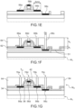
- FIG. 1C A space 51 is thus produced, for example in the form of a groove around a first portion 34a of the ground plane layer 34.
- this groove 51 forms a separation between the first portion 34a of the ground plane layer located under and facing the transistor T 21 and a second portion 34b which can be provided to serve as a rear electrode for another transistor (not shown).
- Localized etching through the opening of a mask (not shown) is typically implemented to cut the ground plane layer 34. This cutting can be carried out by etching using HBr and Cl, in particular when the ground plane layer 34 is made of polysilicon.
- At least one opening 53 is made through the insulating layer 35 revealing a region 34' of the upper face of the portion 34a of the ground plane layer.
- This opening 53 is typically carried out by photolithography then etching through at least one hole in a protective mask (not shown). Dry etching of the dielectric using CH2F2 and SF6 in the case of silicon oxide can for example be used to form this opening 53.
- zones 56a, 56b of metal and semiconductor compound are formed on revealed parts 36' of island 36a, as well as a zone 56c of metal and semiconductor compound. on region 34' of portion 34a of the ground plane layer.
- a layer of metal is typically deposited on the region 34' and the parts 36', and at least one thermal anneal is carried out.
- silicided zones are formed, for example by depositing Nickel and/or NiPt with for example a proportion of 5% to 15% of Pt and by carrying out at least one annealing. thermal.
- annealing at a temperature of for example between 250°C and 350°C for a duration which can be for example of the order of 30s can be carried out. Then, we carry out a selective removal of the unreacted Nickel and we carry out a second annealing to form the NiSi phase.
- the second annealing is typically carried out at a temperature above 350°C for a duration of, for example, around 30 seconds.
- a zone 56d, of metal compound and semiconductor is concomitantly produced on this gate 42.
- silicidated zones 56a, 56b, 56c of significant minimum dimension ⁇ min (dimension measured parallel to the main plane of the substrate , i.e. passing through the substrate and parallel to the plane [O;x;y] of the coordinate system [O;x;y;z]).
- This dimension ⁇ min may depend on the technological node but for a given technological node it is typically greater than that provided for a conventional process and in which the siliciding is carried out at the bottom of holes made through an insulating layer. Indeed, we can provide this dimension ⁇ min greater than that usually provided to form holes intended to accommodate contact pads.
- the ground plane layer is generally doped according to a given type of doping, for example P type, and also includes dopants carrying out doping of the opposite type (here N type) and resulting from doping of regions of the semiconductor island 36a
- the dimensions of the silicided zone 56d of the ground plane layer are advantageously designed so as to occupy and exceed a junction zone made between the two opposite types of doping.
- a first insulating layer 62 is then produced, for example a CESL type layer (for “Contact Etch Stop Layer”) in nitride. silicon and with a thickness e 1 for example between 10 nm and 50 nm.
- the insulating layer 62 can be provided with a thickness e 1 sufficient to fill the space 51, for example in the form of a groove made around the ground plane portion 34a.
- the first insulating layer 62 can then be covered with an insulating layer 64, for example a layer of the PMD type (for “pre-metal dielectric”) in silicon oxide and of thickness e 2 typically greater than e 1 for example included between 100 nm and 700 nm.
- an insulating layer 64 for example a layer of the PMD type (for “pre-metal dielectric”) in silicon oxide and of thickness e 2 typically greater than e 1 for example included between 100 nm and 700 nm.
- holes 66a, 66b, 66c, 66d through the insulating layer(s) 62, 64 and revealing respectively the zones 56a, 56b, 56c, 56d, of metal compound and semiconductor.
- the holes 66a, 66b, 66c, 66d have a critical dimension De, for example between 20 nm and 500 nm, typically less than the minimum dimension ⁇ min of the zones 56a, 56b, 56c, 56d, of metal compound and semi- driver.
- the holes 66a, 66b, 66c, 66d are then filled with conductive material 64, in particular a metal for example such as tungsten ( Figure 1G ).
- holes 66a, 66b, 66c, 66d typically by lithography and etching can be carried out concomitantly or alternatively sequentially. The same goes for filling which can be carried out concomitantly or sequentially.
- a contact pad (not shown on the Figure 1G ) to establish a connection with the first level N 1 can also be formed concomitantly. In this case, it is produced by filling a hole passing through the insulating layer 31 placed between the two levels N 1 and N 2 . This hole is advantageously made so as to pass through the groove 51 made around the ground plane portion 34a.
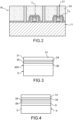
- the second semiconductor layer 36 in which it is planned to form the active zone(s) for transistor(s) of the second level is a surface layer of a massive substrate 3 (“bulk” according to Anglo-Saxon terminology) and on which we then produce the insulating layer 35, then we deposit the ground plane layer and an insulating layer 31 intended to be bonded with the first level N 1 of components.
- the bonding is typically carried out between two insulating layers and in particular of silicon oxide.
- the first level N 1 is coated with such a layer of oxide prior to bonding.
- the semiconductor layer 36 can be detached from the rest of the solid substrate by a smartcut TM type process by creating a weakening zone 300 by implantation of hydrogen ions in the substrate. Polishing and chemical etching steps for example using TMAH (Tetramethylammonium hydroxide) or TEAH (Tetraethyl ammonium hydroxide) can also be carried out in order to remove an unwanted thickness from the massive substrate.
- TMAH Tetramethylammonium hydroxide
- TEAH Tetraethyl ammonium hydroxide
- the second semiconductor layer 36 intended to accommodate the channel region of the transistor T 21 is this time a surface layer of a substrate 4 of the semiconductor on insulator type, for example a substrate of the SOI (silicon on insulator) type ) with a semiconductor support layer 5, an insulating layer 6 typically made of silicon oxide between the support layer 4 and the superficial semiconductor layer 36.
- the insulating layer 35 is then produced, then the ground plane layer 34 and the insulating layer 31 intended to be bonded with the first level N 1 of components.
- the support layer 5 and the insulating layer 6 of the substrate 4 are then eliminated.
- the support layer 5 can be removed for example using polishing and etching steps as mentioned previously for the solid substrate.
- the insulating layer 6 can be removed by etching using HF.
- the ground plane layer 34 when the ground plane layer 34 is provided in doped semiconductor material, this doping is carried out by implantation before assembly by bonding with the first level N 1 .
- this doping can be carried out for example on one or other of the stacks illustrated on the figures 3 and 4 .
- This also makes it possible to carry out an activation annealing of dopants at high temperature without thermal budget constraint linked to the lower level N 1 of components.
- Doping the ground plane layer 34 before bonding can also make it possible to give the ground plane layer 34 a high level of doping by implantation without, however, damaging the semiconductor layer 36 intended to accommodate one or more channel regions of transistors.
- Variant ( figure 5A ) of the example of the production method which has been described previously provides that at the end of the step of cutting the ground plane layer 34, parts 341 of the ground plane layer 34 which are not not covered by an island 36a or an active zone of the second semiconductor layer 36 is revealed.
- the insulating layer 35 is thus removed from the locations which are not covered by the second semiconductor layer 36. Consumption of this insulating layer 35 can be carried out in particular during the etching of the active zone(s), in particular during the definition of island 36a, in particular when this engraving is carried out using HBr and CI for example.
- This insulating layer 35 is typically removed in several stages and in addition to a partial removal carried out during etching making it possible to define the island 36a, revealed parts of this layer 35 are consumed during one or more stages of producing the transistor T 21 , for example during etching of the gate and possibly during one or more cleaning steps, in particular a cleaning step carried out using HF after definition of the gate and before implantation of the source regions and drain. Consumption of the insulating layer 35 can also take place during a possible deoxidation step.
- the ground plane layer 34 is only covered by the insulating layer 35 at the locations facing the island 36a produced by etching the second semiconductor layer 36.
- zones 56a, 56b, of metal compound and semiconductor on the island 36a, as well as a zone 56'c, of metal compound and semiconductor on the revealed parts 341 of the portion 34a or the portions of the ground plane layer.
- these zones 56a, 56b, 56c are produced by a process comprising a metal deposition and one or more thermal annealing(s).
- a silicided zone 56d is also formed on the grid 42.
- the insulation is then carried out around the island 36a and the ground plane portion 34a by depositing the first insulating layer 62 filling the groove 51 then the second insulating layer 64 ( Figure 5C ).
- a conductor pad 86 making contact on the first level N 1 is also formed.
- Such a pad 86 is typically produced by forming a hole passing through the insulation layers 62, 64, this hole passing through the groove 51 and passing through the insulating layer 31 and possibly other underlying layers to reach a zone connection of the first level N 1 .
- FIG. 6 A particular example of realization is illustrated on the Figure 6 in a case where the transistor gate 42 formed on the island 36a extends onto the insulating layer 35 and where a thickness c1 of the insulating layer 35 has been consumed, in particular during etching making it possible to define the island 36a and possibly to steps prior to the deposition of the grid 42 and where a thickness c 2 of the insulating layer 35 was then consumed in particular during the etching making it possible to define the grid 42 and possibly of process steps carried out after the etching of the gate 42 but prior to a doping step by implantation of the island 36a in order to make junctions.
- the insulating layer 35 is made of silicon oxide, it is planned to maintain a thickness h 2 for example greater than 15 nm in the case of an implantation carried out with Boron with an energy between 8 kev and 12 kev and a dose between 1e15 at /cm 3 and 6e15 at/cm 3 and an activation anneal around 1050°C and 14 nm of silicidation with an N-type doped ground plane with 2e20 at/cm 3 .
- limited dose and by “limited energy” we mean by an example for a PMOS transistor: a dose of boron less than 2e15 at /cm 3 and an energy less than 8 keV for a ground plane layer doped N at 2e20 at /cm 3 .
- the insulating layer 35 in the form of a stack of several different dielectric materials 351, 352, 353.
- a stack comprising a layer of silicon nitride placed between two layers of silicon oxide, or a layer of HfO 2 placed between two layers of silicon oxide is produced.
- the fact of providing an insulating layer 35 in the form of such a stack makes it more resistant to etching, and in particular to wet etching using HF.
- the insulating layer 35 is made more resistant to the different etching steps by modifying its composition. For this, we can plan to modify this composition at least on the surface by implantation then annealing.
- this composition at least on the surface by implantation then annealing.
- an implantation of carbon and/or nitrogen atoms can be implemented in order to form SiOC or SiOCN that is more resistant to chemical etching steps, in particular using HF, as silicon oxide.
- Such an implantation can be carried out aimed at modifying the composition of the insulating layer 35 and making it more resistant to etching after having etched the island 36a.
- an implantation of the insulating layer 35 is carried out, in particular using carbon and/or nitrogen.
Landscapes
- Chemical & Material Sciences (AREA)
- Metal-Oxide And Bipolar Metal-Oxide Semiconductor Integrated Circuits (AREA)
- Chemical Kinetics & Catalysis (AREA)
- General Chemical & Material Sciences (AREA)
- Thin Film Transistor (AREA)
- Crystallography & Structural Chemistry (AREA)
Claims (8)
- Verfahren zur Herstellung einer Vorrichtung mit Niveaus (N1, N2) aus überlagerten Komponenten, das in dieser Reihenfolge umfasst:a) Vorsehen, auf einem gegebenen Niveau (N1), das mit einer oder mehreren Komponenten (T11, T12) ausgerüstet ist, die mindestens teilweise in einer ersten Halbleiterschicht (11) ausgebildet sind:
eines Stapels, der eine zweite Halbleiterschicht (36) umfasst, die geeignet ist, mindestens einen Transistorkanal (T21) mit einem Niveau (N2) aufzunehmen, das höher als das gegebene Niveau (N1) ist, wobei der Stapel eine Schicht (34), der Massenebene genannt, aus leitendem oder halbleitendem Material umfasst, das dotiert ist oder geeignet ist, dotiert zu werden, und zwischen der ersten Halbleiterschicht (11) und der zweiten Halbleiterschicht (36) angeordnet ist, sowie eine isolierende Schicht (35), die die Schicht der Massenebene (34) von der zweiten Halbleiterschicht (36) trennt, wobei eine oder mehrere Inseln (36a) in der zweiten Halbleiterschicht (36) definiert sind,b) Bilden eines Gates (42) eines Transistors (T21) auf mindestens einer Insel (36a) unter den einen oder mehreren Inseln,c) Definieren, durch Ätzung, eines oder mehrerer separater Abschnitte (34a, 34b) in der Schicht der Massenebene (34), so dass ein Raum (51) freigemacht wird um mindestens einen ersten geätzten Abschnitt (34a) der Schicht der Massenebene, die unter und gegenüber der Insel (36a) positioniert ist,d) Bilden einer isolierenden Zone um die Insel (36a) und den ersten Abschnitt (34a) durch Abscheiden von mindestens einer Schicht aus isolierendem Material (62), die das Gate (42) und die Insel (36a) bedeckt, wobei die Schicht aus isolierendem Material (62) den Raum (51) um den ersten Abschnitt (34a) der Schicht der Massenebene füllt,e) Bilden von leitenden Pads (66a, 66b, 66c, 86), die durch die Schicht aus isolierendem Material (62) verlaufen, wobei einer oder mehrere der leitenden Pads (66a, 66b) mit der Insel (36a) verbunden sind, wobei mindestens ein anderes leitendes Pad (66c) mit dem ersten Abschnitt (34a) der Schicht der Massenebene (34) verbunden ist. - Verfahren nach Anspruch 1, wobei die Schicht der Massenebene (34) aus halbleitendem Material besteht und wobei, nach dem Definieren des einen oder der mehreren separaten Abschnitte der Schicht der Massenebene und vor dem Abscheiden derSchicht aus isolierendem Material (62), eine oder mehrere Zonen (56a, 56b, 56c) aus Metall- und Halbleiterverbindung gebildet werden, durch:- Abscheiden von mindestens einer Metallschicht auf der Insel (36a) beziehungsweise auf mindestens einem Bereich des ersten Abschnitts (34a),- mindestens ein thermisches Glühen.
- Verfahren nach Anspruch 2, wobei nach der Definition eines oder mehrerer separater Abschnitte der Schicht der Massenebene und vor der Bildung der einen oder der mehreren Zonen (56a, 56b, 56c) der Metall- und der Halbleiterverbindung eine Öffnung (53) in der isolierenden Schicht (35) gebildet wird, die einen Bereich des ersten Abschnitts (34a) freilegt, wobei mindestens eine Zone (56c) der Metall- und Halbleiterverbindung auf dem Niveau des Bereichs des ersten Abschnitts (34a) ausgebildet wird.
- Verfahren nach Anspruch 2, wobei das Verfahren Ätzungen in den Schritten a), b) und c) umfasst, und wobei die isolierende Schicht (35) mit einer Dicke vorgesehen ist, so dass nach den Ätzungen am Ende des Schritts c) und vor der Bildung der Zonen (56a, 56b, 56c) der Metall- und Halbleiterverbindung der erste Abschnitt (34a) in einer Zone freigelegt wird, die sich um die Insel (36a) erstreckt, und nicht gegenüber der Insel (36a) angeordnet ist.
- Verfahren nach einem der Ansprüche 2 bis 4, wobei unter den leitenden Pads (66a, 66b, 66c, 86) mindestens ein gegebenes leitendes Pad (86) so ausgebildet ist, dass es durch den Raum (51) verläuft, der durch das isolierende Material (62) gefüllt ist, wobei das gegebene leitende Pad (86) mit dem ersten Niveau N1 von Komponenten verbunden ist.
- Verfahren nach einem der Ansprüche 1 bis 5, wobei die isolierende Schicht (35), die die Schicht der Massenebene (34) von der zweiten Halbleiterschicht (36) trennt, aus einem Stapel von Schichten (351, 352, 353) verschiedener dielektrischer Materialien gebildet wird.
- Verfahren nach einem der Ansprüche 1 bis 6, wobei die isolierende Schicht (35) aus Siliziumoxid besteht, und wobei vor dem Schritt b) der Bildung des Gates eine Implantation aus Kohlenstoff an der Oberfläche der isolierenden Schicht (35) durchgeführt wird, um SiOC zu bilden oder eine Implantation von Kohlenstoff und Stickstoff, um SiOCN zu bilden.
- Verfahren nach einem der Ansprüche 1 bis 7, wobei vor dem Schritt a) eine Montage durch Verkleben des Stapels auf dem gegebenen Niveau (N1) durchgeführt wird, wobei das Verfahren vor der Montage einen Schritt der Dotierung der Schicht der Massenebene umfasst, wobei die Schicht der Massenebene vorzugsweise mit einer Dotierungskonzentration von 1e20 at/cm3 oder mehr dotiert wird.
Applications Claiming Priority (1)
| Application Number | Priority Date | Filing Date | Title |
|---|---|---|---|
| FR1873965A FR3091016B1 (fr) | 2018-12-19 | 2018-12-19 | Circuit 3d dote d’une isolation mesa pour la zone de plan de masse |
Publications (2)
| Publication Number | Publication Date |
|---|---|
| EP3671836A1 EP3671836A1 (de) | 2020-06-24 |
| EP3671836B1 true EP3671836B1 (de) | 2024-06-12 |
Family
ID=67262401
Family Applications (1)
| Application Number | Title | Priority Date | Filing Date |
|---|---|---|---|
| EP19213818.8A Active EP3671836B1 (de) | 2018-12-19 | 2019-12-05 | 3d schaltung mit einer mesa-isolation für den grundplattenbereich |
Country Status (3)
| Country | Link |
|---|---|
| US (1) | US11139209B2 (de) |
| EP (1) | EP3671836B1 (de) |
| FR (1) | FR3091016B1 (de) |
Families Citing this family (1)
| Publication number | Priority date | Publication date | Assignee | Title |
|---|---|---|---|---|
| CN119361417A (zh) * | 2024-10-17 | 2025-01-24 | 中国科学院微电子研究所 | 基于二次退火的铁电薄膜制备方法及应用 |
Family Cites Families (7)
| Publication number | Priority date | Publication date | Assignee | Title |
|---|---|---|---|---|
| US8536629B2 (en) * | 2009-02-24 | 2013-09-17 | Nec Corporation | Semiconductor device and method for manufacturing the same |
| FR2986370B1 (fr) * | 2012-02-01 | 2014-11-21 | St Microelectronics Sa | Circuit integre 3d |
| US9023688B1 (en) * | 2013-06-09 | 2015-05-05 | Monolithic 3D Inc. | Method of processing a semiconductor device |
| US10297586B2 (en) * | 2015-03-09 | 2019-05-21 | Monolithic 3D Inc. | Methods for processing a 3D semiconductor device |
| KR102230194B1 (ko) | 2014-04-14 | 2021-03-19 | 삼성전자주식회사 | 반도체 소자 |
| FR3037437B1 (fr) | 2015-06-09 | 2018-06-01 | Commissariat Energie Atomique | Realisation d'elements d'interconnexions auto-alignes pour circuit integre 3d |
| FR3059148B1 (fr) | 2016-11-23 | 2019-09-06 | Commissariat A L'energie Atomique Et Aux Energies Alternatives | Realisation d'elements d'interconnexions auto-alignes pour circuit integre 3d |
-
2018
- 2018-12-19 FR FR1873965A patent/FR3091016B1/fr active Active
-
2019
- 2019-12-05 EP EP19213818.8A patent/EP3671836B1/de active Active
- 2019-12-17 US US16/716,659 patent/US11139209B2/en active Active
Also Published As
| Publication number | Publication date |
|---|---|
| US11139209B2 (en) | 2021-10-05 |
| FR3091016B1 (fr) | 2022-12-02 |
| US20200203229A1 (en) | 2020-06-25 |
| EP3671836A1 (de) | 2020-06-24 |
| FR3091016A1 (fr) | 2020-06-26 |
Similar Documents
| Publication | Publication Date | Title |
|---|---|---|
| EP1145300B1 (de) | Verfahren zur herstellung eines mis-transistors auf einem halbleitersubstrat | |
| US12183826B2 (en) | Vertical field effect transistor with low-resistance bottom source-drain contact | |
| KR100333372B1 (ko) | 금속 게이트 모스팻 소자의 제조방법 | |
| EP2562802B1 (de) | Verfahren zur Herstellung eines dreidimensionalen integrierten Schaltkreises | |
| EP3654394B1 (de) | Transistor mit source- und drainblock aus silizid in der nähe des kanals | |
| US9490223B2 (en) | Structure to prevent deep trench moat charging and moat isolation fails | |
| FR2990295A1 (fr) | Procede de formation de contacts de grille, de source et de drain sur un transistor mos | |
| US12453170B2 (en) | Integration of nanosheets with bottom dielectric isolation and ideal diode | |
| FR2860919A1 (fr) | Structures et procedes de fabrication de regions semiconductrices sur isolant | |
| FR3011119A1 (fr) | Procede de realisation d'un transistor | |
| FR3012258A1 (fr) | Procede de realisation de transistors nmos et pmos sur un substrat du type soi, en particulier fdsoi, et circuit integre correspondant | |
| EP2120258B1 (de) | Herstellungsverfahren eines Transistors mit Metallquelle und -abfluss | |
| WO2014037411A1 (fr) | Procédé de réalisation de transistors fet | |
| FR3047352A1 (fr) | Procede de fabrication d'un transistor a dopant localise a l'aplomb de la grille | |
| EP3671836B1 (de) | 3d schaltung mit einer mesa-isolation für den grundplattenbereich | |
| EP1788635B1 (de) | Verfahren zum Herstellen eines Transistors mit selbst justierten Doppel-Gates durch Schrumpfung der Gatestruktur | |
| FR3059148B1 (fr) | Realisation d'elements d'interconnexions auto-alignes pour circuit integre 3d | |
| EP3104402B1 (de) | Herstellung von selbstausgerichteten verbindungselementen für integrierten 3d-schaltkreis | |
| FR3050315B1 (fr) | Transistor a overlap des regions d'acces maitrise | |
| FR3035265A1 (fr) | Procede de fabrication de transistors soi pour une densite d'integration accrue | |
| EP1407486B1 (de) | Herstellungsverfahren für einen transistor auf einem soi-substrat | |
| FR3073667A1 (fr) | Circuit 3d a transistors sans jonction n et p | |
| EP4445427A1 (de) | Verfahren zur herstellung einer 3d-schaltung mit geteilten rekristallisierungs- und dotierungsaktivierungsschritten | |
| EP4391077A1 (de) | Herstellung eines transistors mit einer in der nähe des kanals silizidierten source und drain |
Legal Events
| Date | Code | Title | Description |
|---|---|---|---|
| PUAI | Public reference made under article 153(3) epc to a published international application that has entered the european phase |
Free format text: ORIGINAL CODE: 0009012 |
|
| STAA | Information on the status of an ep patent application or granted ep patent |
Free format text: STATUS: REQUEST FOR EXAMINATION WAS MADE |
|
| 17P | Request for examination filed |
Effective date: 20191205 |
|
| AK | Designated contracting states |
Kind code of ref document: A1 Designated state(s): AL AT BE BG CH CY CZ DE DK EE ES FI FR GB GR HR HU IE IS IT LI LT LU LV MC MK MT NL NO PL PT RO RS SE SI SK SM TR |
|
| AX | Request for extension of the european patent |
Extension state: BA ME |
|
| STAA | Information on the status of an ep patent application or granted ep patent |
Free format text: STATUS: EXAMINATION IS IN PROGRESS |
|
| 17Q | First examination report despatched |
Effective date: 20220202 |
|
| GRAP | Despatch of communication of intention to grant a patent |
Free format text: ORIGINAL CODE: EPIDOSNIGR1 |
|
| STAA | Information on the status of an ep patent application or granted ep patent |
Free format text: STATUS: GRANT OF PATENT IS INTENDED |
|
| INTG | Intention to grant announced |
Effective date: 20240103 |
|
| GRAS | Grant fee paid |
Free format text: ORIGINAL CODE: EPIDOSNIGR3 |
|
| GRAA | (expected) grant |
Free format text: ORIGINAL CODE: 0009210 |
|
| STAA | Information on the status of an ep patent application or granted ep patent |
Free format text: STATUS: THE PATENT HAS BEEN GRANTED |
|
| AK | Designated contracting states |
Kind code of ref document: B1 Designated state(s): AL AT BE BG CH CY CZ DE DK EE ES FI FR GB GR HR HU IE IS IT LI LT LU LV MC MK MT NL NO PL PT RO RS SE SI SK SM TR |
|
| REG | Reference to a national code |
Ref country code: GB Ref legal event code: FG4D Free format text: NOT ENGLISH |
|
| REG | Reference to a national code |
Ref country code: CH Ref legal event code: EP |
|
| REG | Reference to a national code |
Ref country code: DE Ref legal event code: R096 Ref document number: 602019053497 Country of ref document: DE |
|
| REG | Reference to a national code |
Ref country code: IE Ref legal event code: FG4D Free format text: LANGUAGE OF EP DOCUMENT: FRENCH |
|
| PG25 | Lapsed in a contracting state [announced via postgrant information from national office to epo] |
Ref country code: BG Free format text: LAPSE BECAUSE OF FAILURE TO SUBMIT A TRANSLATION OF THE DESCRIPTION OR TO PAY THE FEE WITHIN THE PRESCRIBED TIME-LIMIT Effective date: 20240612 |
|
| PG25 | Lapsed in a contracting state [announced via postgrant information from national office to epo] |
Ref country code: HR Free format text: LAPSE BECAUSE OF FAILURE TO SUBMIT A TRANSLATION OF THE DESCRIPTION OR TO PAY THE FEE WITHIN THE PRESCRIBED TIME-LIMIT Effective date: 20240612 Ref country code: FI Free format text: LAPSE BECAUSE OF FAILURE TO SUBMIT A TRANSLATION OF THE DESCRIPTION OR TO PAY THE FEE WITHIN THE PRESCRIBED TIME-LIMIT Effective date: 20240612 |
|
| REG | Reference to a national code |
Ref country code: LT Ref legal event code: MG9D |
|
| PG25 | Lapsed in a contracting state [announced via postgrant information from national office to epo] |
Ref country code: GR Free format text: LAPSE BECAUSE OF FAILURE TO SUBMIT A TRANSLATION OF THE DESCRIPTION OR TO PAY THE FEE WITHIN THE PRESCRIBED TIME-LIMIT Effective date: 20240913 |
|
| REG | Reference to a national code |
Ref country code: NL Ref legal event code: MP Effective date: 20240612 |
|
| PG25 | Lapsed in a contracting state [announced via postgrant information from national office to epo] |
Ref country code: ES Free format text: LAPSE BECAUSE OF FAILURE TO SUBMIT A TRANSLATION OF THE DESCRIPTION OR TO PAY THE FEE WITHIN THE PRESCRIBED TIME-LIMIT Effective date: 20240612 |
|
| PG25 | Lapsed in a contracting state [announced via postgrant information from national office to epo] |
Ref country code: LV Free format text: LAPSE BECAUSE OF FAILURE TO SUBMIT A TRANSLATION OF THE DESCRIPTION OR TO PAY THE FEE WITHIN THE PRESCRIBED TIME-LIMIT Effective date: 20240612 |
|
| RAP4 | Party data changed (patent owner data changed or rights of a patent transferred) |
Owner name: COMMISSARIAT A L'ENERGIE ATOMIQUE ET AUX ENERGIESALTERNATIVES |
|
| PG25 | Lapsed in a contracting state [announced via postgrant information from national office to epo] |
Ref country code: NO Free format text: LAPSE BECAUSE OF FAILURE TO SUBMIT A TRANSLATION OF THE DESCRIPTION OR TO PAY THE FEE WITHIN THE PRESCRIBED TIME-LIMIT Effective date: 20240912 Ref country code: LV Free format text: LAPSE BECAUSE OF FAILURE TO SUBMIT A TRANSLATION OF THE DESCRIPTION OR TO PAY THE FEE WITHIN THE PRESCRIBED TIME-LIMIT Effective date: 20240612 Ref country code: HR Free format text: LAPSE BECAUSE OF FAILURE TO SUBMIT A TRANSLATION OF THE DESCRIPTION OR TO PAY THE FEE WITHIN THE PRESCRIBED TIME-LIMIT Effective date: 20240612 Ref country code: GR Free format text: LAPSE BECAUSE OF FAILURE TO SUBMIT A TRANSLATION OF THE DESCRIPTION OR TO PAY THE FEE WITHIN THE PRESCRIBED TIME-LIMIT Effective date: 20240913 Ref country code: FI Free format text: LAPSE BECAUSE OF FAILURE TO SUBMIT A TRANSLATION OF THE DESCRIPTION OR TO PAY THE FEE WITHIN THE PRESCRIBED TIME-LIMIT Effective date: 20240612 Ref country code: ES Free format text: LAPSE BECAUSE OF FAILURE TO SUBMIT A TRANSLATION OF THE DESCRIPTION OR TO PAY THE FEE WITHIN THE PRESCRIBED TIME-LIMIT Effective date: 20240612 Ref country code: BG Free format text: LAPSE BECAUSE OF FAILURE TO SUBMIT A TRANSLATION OF THE DESCRIPTION OR TO PAY THE FEE WITHIN THE PRESCRIBED TIME-LIMIT Effective date: 20240612 Ref country code: RS Free format text: LAPSE BECAUSE OF FAILURE TO SUBMIT A TRANSLATION OF THE DESCRIPTION OR TO PAY THE FEE WITHIN THE PRESCRIBED TIME-LIMIT Effective date: 20240912 |
|
| PG25 | Lapsed in a contracting state [announced via postgrant information from national office to epo] |
Ref country code: NL Free format text: LAPSE BECAUSE OF FAILURE TO SUBMIT A TRANSLATION OF THE DESCRIPTION OR TO PAY THE FEE WITHIN THE PRESCRIBED TIME-LIMIT Effective date: 20240612 |
|
| REG | Reference to a national code |
Ref country code: AT Ref legal event code: MK05 Ref document number: 1694968 Country of ref document: AT Kind code of ref document: T Effective date: 20240612 |
|
| REG | Reference to a national code |
Ref country code: DE Ref legal event code: R079 Ref document number: 602019053497 Country of ref document: DE Free format text: PREVIOUS MAIN CLASS: H01L0027120000 Ipc: H10D0086000000 |
|
| PG25 | Lapsed in a contracting state [announced via postgrant information from national office to epo] |
Ref country code: NL Free format text: LAPSE BECAUSE OF FAILURE TO SUBMIT A TRANSLATION OF THE DESCRIPTION OR TO PAY THE FEE WITHIN THE PRESCRIBED TIME-LIMIT Effective date: 20240612 |
|
| PG25 | Lapsed in a contracting state [announced via postgrant information from national office to epo] |
Ref country code: PT Free format text: LAPSE BECAUSE OF FAILURE TO SUBMIT A TRANSLATION OF THE DESCRIPTION OR TO PAY THE FEE WITHIN THE PRESCRIBED TIME-LIMIT Effective date: 20241014 |
|
| PG25 | Lapsed in a contracting state [announced via postgrant information from national office to epo] |
Ref country code: PT Free format text: LAPSE BECAUSE OF FAILURE TO SUBMIT A TRANSLATION OF THE DESCRIPTION OR TO PAY THE FEE WITHIN THE PRESCRIBED TIME-LIMIT Effective date: 20241014 |
|
| PG25 | Lapsed in a contracting state [announced via postgrant information from national office to epo] |
Ref country code: PL Free format text: LAPSE BECAUSE OF FAILURE TO SUBMIT A TRANSLATION OF THE DESCRIPTION OR TO PAY THE FEE WITHIN THE PRESCRIBED TIME-LIMIT Effective date: 20240612 |
|
| PG25 | Lapsed in a contracting state [announced via postgrant information from national office to epo] |
Ref country code: EE Free format text: LAPSE BECAUSE OF FAILURE TO SUBMIT A TRANSLATION OF THE DESCRIPTION OR TO PAY THE FEE WITHIN THE PRESCRIBED TIME-LIMIT Effective date: 20240612 |
|
| PG25 | Lapsed in a contracting state [announced via postgrant information from national office to epo] |
Ref country code: IS Free format text: LAPSE BECAUSE OF FAILURE TO SUBMIT A TRANSLATION OF THE DESCRIPTION OR TO PAY THE FEE WITHIN THE PRESCRIBED TIME-LIMIT Effective date: 20241012 Ref country code: AT Free format text: LAPSE BECAUSE OF FAILURE TO SUBMIT A TRANSLATION OF THE DESCRIPTION OR TO PAY THE FEE WITHIN THE PRESCRIBED TIME-LIMIT Effective date: 20240612 |
|
| PG25 | Lapsed in a contracting state [announced via postgrant information from national office to epo] |
Ref country code: CZ Free format text: LAPSE BECAUSE OF FAILURE TO SUBMIT A TRANSLATION OF THE DESCRIPTION OR TO PAY THE FEE WITHIN THE PRESCRIBED TIME-LIMIT Effective date: 20240612 |
|
| PG25 | Lapsed in a contracting state [announced via postgrant information from national office to epo] |
Ref country code: SK Free format text: LAPSE BECAUSE OF FAILURE TO SUBMIT A TRANSLATION OF THE DESCRIPTION OR TO PAY THE FEE WITHIN THE PRESCRIBED TIME-LIMIT Effective date: 20240612 Ref country code: RO Free format text: LAPSE BECAUSE OF FAILURE TO SUBMIT A TRANSLATION OF THE DESCRIPTION OR TO PAY THE FEE WITHIN THE PRESCRIBED TIME-LIMIT Effective date: 20240612 |
|
| PG25 | Lapsed in a contracting state [announced via postgrant information from national office to epo] |
Ref country code: SM Free format text: LAPSE BECAUSE OF FAILURE TO SUBMIT A TRANSLATION OF THE DESCRIPTION OR TO PAY THE FEE WITHIN THE PRESCRIBED TIME-LIMIT Effective date: 20240612 |
|
| PG25 | Lapsed in a contracting state [announced via postgrant information from national office to epo] |
Ref country code: SM Free format text: LAPSE BECAUSE OF FAILURE TO SUBMIT A TRANSLATION OF THE DESCRIPTION OR TO PAY THE FEE WITHIN THE PRESCRIBED TIME-LIMIT Effective date: 20240612 Ref country code: SK Free format text: LAPSE BECAUSE OF FAILURE TO SUBMIT A TRANSLATION OF THE DESCRIPTION OR TO PAY THE FEE WITHIN THE PRESCRIBED TIME-LIMIT Effective date: 20240612 Ref country code: RO Free format text: LAPSE BECAUSE OF FAILURE TO SUBMIT A TRANSLATION OF THE DESCRIPTION OR TO PAY THE FEE WITHIN THE PRESCRIBED TIME-LIMIT Effective date: 20240612 Ref country code: PL Free format text: LAPSE BECAUSE OF FAILURE TO SUBMIT A TRANSLATION OF THE DESCRIPTION OR TO PAY THE FEE WITHIN THE PRESCRIBED TIME-LIMIT Effective date: 20240612 Ref country code: IS Free format text: LAPSE BECAUSE OF FAILURE TO SUBMIT A TRANSLATION OF THE DESCRIPTION OR TO PAY THE FEE WITHIN THE PRESCRIBED TIME-LIMIT Effective date: 20241012 Ref country code: EE Free format text: LAPSE BECAUSE OF FAILURE TO SUBMIT A TRANSLATION OF THE DESCRIPTION OR TO PAY THE FEE WITHIN THE PRESCRIBED TIME-LIMIT Effective date: 20240612 Ref country code: CZ Free format text: LAPSE BECAUSE OF FAILURE TO SUBMIT A TRANSLATION OF THE DESCRIPTION OR TO PAY THE FEE WITHIN THE PRESCRIBED TIME-LIMIT Effective date: 20240612 Ref country code: AT Free format text: LAPSE BECAUSE OF FAILURE TO SUBMIT A TRANSLATION OF THE DESCRIPTION OR TO PAY THE FEE WITHIN THE PRESCRIBED TIME-LIMIT Effective date: 20240612 |
|
| PG25 | Lapsed in a contracting state [announced via postgrant information from national office to epo] |
Ref country code: IT Free format text: LAPSE BECAUSE OF FAILURE TO SUBMIT A TRANSLATION OF THE DESCRIPTION OR TO PAY THE FEE WITHIN THE PRESCRIBED TIME-LIMIT Effective date: 20240612 |
|
| REG | Reference to a national code |
Ref country code: DE Ref legal event code: R097 Ref document number: 602019053497 Country of ref document: DE |
|
| PG25 | Lapsed in a contracting state [announced via postgrant information from national office to epo] |
Ref country code: DK Free format text: LAPSE BECAUSE OF FAILURE TO SUBMIT A TRANSLATION OF THE DESCRIPTION OR TO PAY THE FEE WITHIN THE PRESCRIBED TIME-LIMIT Effective date: 20240612 |
|
| PLBE | No opposition filed within time limit |
Free format text: ORIGINAL CODE: 0009261 |
|
| STAA | Information on the status of an ep patent application or granted ep patent |
Free format text: STATUS: NO OPPOSITION FILED WITHIN TIME LIMIT |
|
| 26N | No opposition filed |
Effective date: 20250313 |
|
| PG25 | Lapsed in a contracting state [announced via postgrant information from national office to epo] |
Ref country code: MC Free format text: LAPSE BECAUSE OF FAILURE TO SUBMIT A TRANSLATION OF THE DESCRIPTION OR TO PAY THE FEE WITHIN THE PRESCRIBED TIME-LIMIT Effective date: 20240612 |
|
| REG | Reference to a national code |
Ref country code: CH Ref legal event code: PL |
|
| PG25 | Lapsed in a contracting state [announced via postgrant information from national office to epo] |
Ref country code: LU Free format text: LAPSE BECAUSE OF NON-PAYMENT OF DUE FEES Effective date: 20241205 |
|
| PG25 | Lapsed in a contracting state [announced via postgrant information from national office to epo] |
Ref country code: SE Free format text: LAPSE BECAUSE OF FAILURE TO SUBMIT A TRANSLATION OF THE DESCRIPTION OR TO PAY THE FEE WITHIN THE PRESCRIBED TIME-LIMIT Effective date: 20240612 |
|
| REG | Reference to a national code |
Ref country code: BE Ref legal event code: MM Effective date: 20241231 |
|
| PG25 | Lapsed in a contracting state [announced via postgrant information from national office to epo] |
Ref country code: BE Free format text: LAPSE BECAUSE OF NON-PAYMENT OF DUE FEES Effective date: 20241231 |
|
| PG25 | Lapsed in a contracting state [announced via postgrant information from national office to epo] |
Ref country code: CH Free format text: LAPSE BECAUSE OF NON-PAYMENT OF DUE FEES Effective date: 20241231 |
|
| PG25 | Lapsed in a contracting state [announced via postgrant information from national office to epo] |
Ref country code: IE Free format text: LAPSE BECAUSE OF NON-PAYMENT OF DUE FEES Effective date: 20241205 |
|
| PGFP | Annual fee paid to national office [announced via postgrant information from national office to epo] |
Ref country code: GB Payment date: 20251229 Year of fee payment: 7 |
|
| PGFP | Annual fee paid to national office [announced via postgrant information from national office to epo] |
Ref country code: FR Payment date: 20251222 Year of fee payment: 7 |
|
| PG25 | Lapsed in a contracting state [announced via postgrant information from national office to epo] |
Ref country code: CY Free format text: LAPSE BECAUSE OF FAILURE TO SUBMIT A TRANSLATION OF THE DESCRIPTION OR TO PAY THE FEE WITHIN THE PRESCRIBED TIME-LIMIT; INVALID AB INITIO Effective date: 20191205 |
|
| PGFP | Annual fee paid to national office [announced via postgrant information from national office to epo] |
Ref country code: DE Payment date: 20251222 Year of fee payment: 7 |