EP3671871A1 - Herstellungsverfahren einer vorrichtung, die ein material umfasst, das nach einer elektrischen polarisierung elektrische eigenschaften erwirbt - Google Patents
Herstellungsverfahren einer vorrichtung, die ein material umfasst, das nach einer elektrischen polarisierung elektrische eigenschaften erwirbt Download PDFInfo
- Publication number
- EP3671871A1 EP3671871A1 EP19216374.9A EP19216374A EP3671871A1 EP 3671871 A1 EP3671871 A1 EP 3671871A1 EP 19216374 A EP19216374 A EP 19216374A EP 3671871 A1 EP3671871 A1 EP 3671871A1
- Authority
- EP
- European Patent Office
- Prior art keywords
- layer
- polarization
- electrical
- manufacturing
- stack
- Prior art date
- Legal status (The legal status is an assumption and is not a legal conclusion. Google has not performed a legal analysis and makes no representation as to the accuracy of the status listed.)
- Granted
Links
Images


Classifications
-
- H—ELECTRICITY
- H10—SEMICONDUCTOR DEVICES; ELECTRIC SOLID-STATE DEVICES NOT OTHERWISE PROVIDED FOR
- H10N—ELECTRIC SOLID-STATE DEVICES NOT OTHERWISE PROVIDED FOR
- H10N15/00—Thermoelectric devices without a junction of dissimilar materials; Thermomagnetic devices, e.g. using the Nernst-Ettingshausen effect
- H10N15/10—Thermoelectric devices using thermal change of the dielectric constant, e.g. working above and below the Curie point
- H10N15/15—Thermoelectric active materials
-
- H—ELECTRICITY
- H10—SEMICONDUCTOR DEVICES; ELECTRIC SOLID-STATE DEVICES NOT OTHERWISE PROVIDED FOR
- H10N—ELECTRIC SOLID-STATE DEVICES NOT OTHERWISE PROVIDED FOR
- H10N15/00—Thermoelectric devices without a junction of dissimilar materials; Thermomagnetic devices, e.g. using the Nernst-Ettingshausen effect
- H10N15/10—Thermoelectric devices using thermal change of the dielectric constant, e.g. working above and below the Curie point
-
- H—ELECTRICITY
- H10—SEMICONDUCTOR DEVICES; ELECTRIC SOLID-STATE DEVICES NOT OTHERWISE PROVIDED FOR
- H10N—ELECTRIC SOLID-STATE DEVICES NOT OTHERWISE PROVIDED FOR
- H10N30/00—Piezoelectric or electrostrictive devices
- H10N30/01—Manufacture or treatment
- H10N30/04—Treatments to modify a piezoelectric or electrostrictive property, e.g. polarisation characteristics, vibration characteristics or mode tuning
- H10N30/045—Treatments to modify a piezoelectric or electrostrictive property, e.g. polarisation characteristics, vibration characteristics or mode tuning by polarising
Definitions
- the present invention relates to a method of manufacturing a device comprising at least one layer of material acquiring an electrical property after being subjected to polarization, for example comprising a material becoming pyroelectric by polarization.
- the pyroelectric effect is used, i.e. the generation of charges due to a temperature variation.
- a thermal fingerprint sensor comprises a matrix of pixels, each capable of generating charges by variation of temperature.
- Each pixel has a pyroelectric material between two electrodes, each pixel is individually addressable to detect the amount of charge produced by each of the pixels.
- a fingerprint has peaks and valleys and the contact between a pixel and a peak or valley causes a temperature variation, which is different depending on whether it is a peak or a valley.
- the pixels are heated in order to avoid a thermal equilibrium between the sensor and the surface of the finger
- PVDF poly (vinylidene fluoride)
- PVDF-TrFE tri fluoro ethylene
- one or more transistors can be implemented.
- At least three transistors can be implemented at the level of each pixel to read the voltage: a transistor ensuring the amplification of the signal, a second transistor allowing the selection of the pixel and a third transistor allowing to put the voltage at a known value at the start of acquisition.
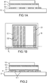
- the device comprises a substrate S, a layer of PVDF C1 between a metallic conductive layer forming common electrode E1 and a plurality of parallel electrically conductive strips forming individual electrodes E2.
- the device comprises a PVDF layer between a metallic conductive layer forming a common electrode and a plurality of conductive zones at the level of each pixel.
- the PVDF becomes pyroelectric after being polarized.
- the voltage to be applied to polarize the PVDF is between 75 V and 150 V per ⁇ m of thickness of PVDF. This polarization is carried out between the common electrode and the individual electrodes. In addition, if this polarization is to be carried out when piloting transistors are already in place, this voltage level can cause damage or even destruction of the transistors.
- all the individual electrodes E2 are short-circuited, for example by providing an electrical track P1 connecting all the individual electrodes as shown in the figure 1B , which makes it easier to apply a bias voltage across the PVDF layer.
- this short-circuiting must be removed in order to make the device usable, for this the electrical track is removed after the polarization.
- This electrical track P1 is removed by cutting the substrate (along the dotted line on the figure 1B ), this results in a loss of material and available space. In addition, this may result in chips and / or debris which can disturb the proper functioning of the device. In addition there is a risk that the cutting is not successful and that the device is unusable.
- the previously stated aim is achieved with a manufacturing process using a layer of a material capable of acquiring at least one electrical property after having been subjected to polarization, a common electrode and individual electrodes on either side of the material capable of acquiring electrical property, and a so-called polarization layer in contact with all the individual electrodes, the polarization layer having the property of being electrically conductive, and after application of a specific treatment, of being electrically insulating.
- PVDF polyvinylidene fluoride
- the manufacturing process uses a dedicated layer to polarize the material and give it its electrical property, this layer being rendered non-functional after the material has acquired its electrical property.
- such a material is a crosslinkable adhesive containing one or more initiation salts of photopolymerization, such as the epoxy adhesive LP 655 manufactured by DELO.
- the salts present in the formulation provide ionic conduction which disappears after UV exposure, which makes the electrical insulating glue during its crosslinking under UV.
- the polarization layer is arranged between the layer of material to be polarized and the individual electrodes. More advantageously, the layer is arranged between the substrate and the individual electrodes, which limits the interactions between the material to be polarized, for example PVDF and the material of the polarization layer, the effects of which are not known for long. term.
- the polarization layer can be located.
- the method according to the invention has the advantage of not requiring any cutting step or any other step liable to pollute the device.
- the elimination of short circuits is simple.
- the application of ultraviolet radiation in the case of LP 655 adhesive has no harmful effect on the rest of the components of the device.
- contact pads are provided intended to at least check after treatment if the polarization layer has actually become electrical insulator.
- the method according to the invention is advantageously implemented in the manufacture of thermal pattern sensors, in particular fingerprint sensors.
- the invention is all the more advantageous for devices implementing transistors, in fact the transistors are becoming smaller and more and more sensitive to the electric field.
- the short-circuiting thanks to the polarization layer makes it possible to protect them effectively.
- the material of the third layer becomes pyroelectric by applying a given polarization.
- the polarization layer is formed between the first layer and the third layer. According to another exemplary embodiment, the polarization layer is formed between the substrate and the first layer.
- the conductors of the first layer are made in the form of strips and the polarization layer is formed so as to be in contact with at least part of each of the strips.
- the polarization layer can be formed so as to be in contact with a longitudinal end of the strips.
- the method comprises the step of producing two electrical contacts in electrical contact with the bias layer, said electrical contacts being intended to at least verify the electrical conductivity of said bias layer at least after the treatment.
- the manufacturing method advantageously comprises the step of producing at least two transistors, each transistor being connected to an electrical conductor, the biasing layer being formed so as to be electrically connected at least to the drains of the transistors, and during the 'step c) the polarization layer, the drains, the sources and the grids are short-circuited.
- the polarization layer is a crosslinkable adhesive containing one or more crosslinking initiation salts, and the treatment is exposure to ultraviolet radiation.
- the material of the third layer may include poly (vinylidene fluoride) or one of its derivatives.
- the substrate is made of a material transparent to ultraviolet radiation and the exposure is carried out through the substrate.
- step d only portions of the polarization layer located between the conductors are made electrically insulating.
- the sun is made through a mask.
- the present invention also relates to a method of manufacturing a thermal pattern sensor comprising the manufacture of a device comprising a stack by the method according to the invention, the step of producing, on said stack, electrically conductive lines forming a heat source and the step of producing an encapsulation layer.
- the present invention also relates to a stack in order to produce a device comprising at least a first layer comprising at least two electrical conductors electrically isolated from each other, a second layer comprising at least one electrical conductor, a third layer of a material having at least one electrical property after electrical polarization, said third layer being disposed between the first layer and the second layer, said stack being obtained by implementing the manufacturing method according to the invention, said stack comprising the first layer, the second layer, the third layer, the material of the third layer not having said electrical property and a polarization layer of a material which has a first state in which it is electrically conductive and a second state in which it is electrically insulating, the transition from the first state to the second state being obtained by application of a treatment to said second material, said polarization layer being produced so as to be initially in its first state, said layer of polarization being in electrical contact with the electrical conductors of the first layer.
- the material of the third layer is poly (vinylidene fluoride) or one of its derivatives
- the material of the polarization layer is a crosslinkable adhesive containing one or more crosslinking initiation salts, for example an epoxy adhesive, said treatment being exposure to ultraviolet radiation.
- the invention will be described mainly in the context of the manufacture of a stack comprising PVDF in order to make it pyroelectric, with a view to an application to the production of fingerprint sensors, and more generally the production of thermal sensors.
- the invention can be applied to all devices the production of which requires a polarization step in order to acquire a material's electrical property, examples of which will be given below.
- an insulating or conductive material is an electrical insulating material or electrical conductor respectively, unless this is explicitly stated.
- the term “electrical property” of a material means a property by which the material is capable of generating a voltage or a current, for example when it is subjected to a temperature variation, it is a question pyroelectricity, or when subjected to deformation, it is piezoelectricity, or when it is the seat of permanent polarization after being subjected to polarization, such as the electrets.
- polarization such as the electrets.
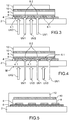
- the stack EP1 comprises in this order a substrate 2, a layer 4 comprising a plurality of parallel electrically conductive strips 4.1 intended to form individual electrodes.
- the stack EP1 comprises a polarization layer 6, a layer 8 of material capable of having pyroelectric properties under the effect of a polarization, an electrically conductive layer 10 intended to form an electrode common to the right of the individual electrodes.
- a layer 12 intended to protect the stack is formed on the layer 10.
- the pyroelectric material of layer 8 can for example be a polyvinylidene fluoride or PVDF, a polyvinylidene-trifluoroethylene or P (VDF-TrFE), a ceramic such as PZT (lead titano-zirconate, or "Lead Zirconate Titanate "In English), crystals such as those known by the acronym TGS (Tris Glycine SDF) or LiTaO 3 crystals.
- PVDF polyvinylidene fluoride
- VDF-TrFE polyvinylidene-trifluoroethylene
- PZT lead titano-zirconate, or "Lead Zirconate Titanate "In English
- crystals such as those known by the acronym TGS (Tris Glycine SDF) or LiTaO 3 crystals.
- the common electrode 10 is connected to a given voltage, for example to ground.
- the substrate is for example electrical insulator, for example in a rigid material such as glass, or a flexible material, such as plastic material such as polyethylene (PET), poly (ethylene naphthalate) (PEN), polyurethane (PU) or polydimethyl (siloxane) (PDMS).
- plastic material such as polyethylene (PET), poly (ethylene naphthalate) (PEN), polyurethane (PU) or polydimethyl (siloxane) (PDMS).
- the device can be manufactured using a CMOS technology on a silicon substrate or on a silicon substrate on SOI insulator (Silicon on Insulator).
- each individual electrode means an electrode intended to form with the common electrode a part at most of the pixels.
- each individual electrode forms a column type pixel with the PVDF and the common electrode.
- heating lines perpendicular to the individual electrodes are formed, the crossing of a heating line and an individual electrode being considered as a pixel.
- the polarization layer 6 comprises a material which offers a state in which it is electrically conductive and a state, after application of a given treatment, in which it is electrically insulating.
- the term “electrical conductor” means a material which is sufficiently conductive to ensure a short-circuiting of the electrodes and / or of the transistors, and to allow the application of a bias voltage sufficient to make the material of the layer 8 pyroelectric in a few seconds up to 1 min. Even a material with very low electrical conductivity may be suitable.
- electrical insulating material means a material which is sufficiently insulating so that the quantity of charges produced at the level of a pixel can be detected separately from those generated at the level of the other pixels. For example, it is sought to have a current circulation in the polarization layer after treatment of at least 100 times less than the circulation in the individual electrodes.
- the material of the polarization layer 6 is a crosslinkable adhesive containing one or more crosslinking initiation salts, for example an epoxy adhesive.
- crosslinking initiation salts for example an epoxy adhesive.
- cationic photoinitiators such as the diaryliodonium or triarylsulfonium salts are initiation crosslinking salts suitable for the present invention.
- the initiation salt is ionic conductor, which makes the material weakly electrically conductive before crosslinking. After crosslinking, the material becomes electrically insulating.
- the epoxy adhesive produced by the company DELO is, for example, an adhesive whose salts added to the formulation are salts which initiate UV photopolymerization.
- the polarization layer comprises epoxy glue LP655 manufactured by DELO which passes from a conductive state to an electrical insulating state by crosslinking under exposure to ultraviolet (UV) radiation at a wavelength of about 365 nm.
- UV radiation ultraviolet
- the polarization layer 6 has for example a thickness of a hundred nm to a few ⁇ m.
- the figure 10 illustrates the evolution of electrical conductivity as a function of the level of crosslinking of the LP655 adhesive. It represents the variation of the current I in Amperes between two electric conductive bars connected by a drop of glue LP655 as a function of the voltage U in Volt.
- Each curve represents an electrical conductivity for a crosslinking time under UV.
- the To curve corresponds to the bars without drop of LP655, the current does not pass.
- T1 corresponding to a crosslinking time of 60 s, corresponds to the current flowing between the conductors with a drop of non-crosslinked LP 655 and therefore relatively conductive.
- the curves T2 to T5 correspond, in this order to states which are more and more crosslinked (crosslinking time under UV longer and longer) and less and less conductive. It can be seen that the electrical conductivity for the longest crosslinking time T5 is practically identical to the conductivity To, ie without drop. The material of layer 6 for a crosslinking time corresponding to T5 is therefore completely insulating.
- the polarization layer 6 extends so as to be in contact with all the individual electrodes, in order to short-circuit all the individual electrodes.
- the polarization layer 6 does not necessarily entirely cover the individual electrodes.
- the polarization layer 6 is formed between the substrate 2 and the individual electrodes.
- the polarization layer 6 provides the connection between all of the individual electrodes.
- the PVDF layer is formed on the individual electrodes. Due to the manufacturing process, it is also deposited between the individual electrodes and is in contact with the polarization layer 6.
- the PVDF layer is then made pyroelectric.
- a bias voltage is applied between the common electrode 10 and one of the individual electrodes, or even between the common electrode and the bias layer, to apply a sufficient voltage in order to make the PVDF pyroelectric.
- the bias voltage is around 300 V for a few seconds.
- the PVDF zones located to the right of the individual electrodes are made pyroelectric.
- This example is particularly advantageous, since the production of the polarization layer on the substrate is very simple and does not require structuring of the latter.
- the polarization layer 6 thus arranged does not form any additional capacitance between the individual electrodes and the common electrode.
- the entire polarization layer is made electrically insulating, for example by carrying out UV treatment through the substrate chosen to be transparent to UV.
- the polarization layer 6 is formed on the individual electrodes 4.1.
- the polarization layer is such that it allows all the individual electrodes to be connected.
- the polarization layer 6 only partially covers the individual electrode located at the right end in the representation of the figure 2 , but this partial overlap is sufficient to connect it to the other individual electrodes.
- the PVDF layer is then made pyroelectric.
- a bias voltage is applied between the common electrode 10 and one of the individual electrodes, or even between the common electrode and the bias layer, to apply a sufficient voltage in order to make the PVDF pyroelectric.
- the bias voltage is of the order of 300V.
- the implementation of the polarization layer simply makes it possible to apply a polarization voltage in a single step to all the zones of PVDF, in particular those located at the right of the individual electrodes.
- a treatment is applied to the polarization layer 6 in order to make it entirely electrically insulating.
- the polarization layer is made of LP 655 epoxy adhesive, it is crosslinked by UV exposure at a wavelength of about 365 nm.
- the duration of the insolation is chosen to ensure that the electrical conductivity of the adhesive is low enough to be considered as insulating, and that the individual electrodes are no longer electrically connected to each other.
- the duration of exposure is also sufficient for the adhesive to act as an adhesive and to be sufficiently hard.
- the polarization of PVDF is typically obtained by applying an electric field of 100 volts for a PVDF layer of 1 ⁇ m. In the case of a 3 nm PVDF layer, an electric field of around 300 volts is applied.
- the polarization layer is exposed through the substrate which is chosen to be transparent to UV radiation, for example this is made of glass or plastic, and through the individual electrodes which are chosen to be thin enough to be transparent to UV radiation.
- UV exposure is carried out through the common electrode when the material of the common electrode is sufficiently transparent to UV radiation, which is for example the case of an organic common electrode, for example made of PEDOT: PSS (mixture of poly (3,4-ethylenedioxythiophene) (PEDOT) and sodium poly (styrene sulfonate) (PSS)).
- PEDOT poly (3,4-ethylenedioxythiophene)
- PSS sodium poly (styrene sulfonate)
- the entire polarization layer 6 is made insulating.
- the presence of the polarizing layer 6 which is now electrically insulating adds a capacity in series, decreasing the total capacity of the pixel, which does not significantly disturb the operation of the device in the case of reading under load.
- its presence can be advantageous since the voltage produced is increased for the same amount of charge since the total capacity of the pixel is reduced. The detection sensitivity is then increased.
- this insulating layer in contact with the PVDF makes it possible to further reduce the leakage current through the PVDF, which is already low due to the very good electrical insulation provided by the PVDF.
- a substrate 2 sufficiently transparent to UV radiation, such as glass or a plastic material, to allow sunshine through the substrate, as shown by the UV arrows, and we choose individual metal electrodes that are sufficiently thick. so as not to be transparent to UV.
- the UV1 rays insolate the polarization layer 6, and the UV2 rays are stopped by the electrodes 4.1. It follows that at the end of the insolation step, the polarization layer 6 retains conductive areas 6.1 in line with the individual electrodes, separated by insulating areas 6.2 between the individual electrodes.
- the conductive areas 6.1 form an extension of the individual electrodes, in the direction of the thickness of the electrodes.
- a mask M is used to mask the polarization layer from UV radiation.
- the mask M is placed under the substrate and is in line with each individual electrode.
- the mask is placed above the common electrode when the exposure is made through the common electrode.
- the mask is for example used when the individual electrodes are too transparent to UV rays to prevent crosslinking.
- the mask is similar to those commonly used in microelectronic processes.
- the UV1 rays insolate the polarization layer 6, and the UV2 rays are stopped by the mask.
- the polarization layer 6 comprises electrical insulating portions 6.2 which electrically insulate the individual electrodes 4.1.
- the processing depends on the material of the polarization layer. In the case of sunshine, it will be made at a wavelength capable of crosslinking the material, which may be different from that of UV radiation.
- two electrical contact pads 14 are formed in the polarization layer 6 outside of the stack with the PVDF layer, and on either side of the stack in the plane of the polarization layer. For example, by applying a voltage between the pads 14, a current greater than a given threshold is measured if the bias layer is electrically conductive, and a current is measured below the given threshold if the bias layer is insulating.
- the contact pads 14 also make it possible to measure the conduction of the polarization layer before the polarization of the PVDF and to verify that it is sufficiently conductive, one of the contact pads can be used with the common electrode, to apply the bias voltage to the PVDF layer.
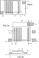
- the polarization layer 6 ′ is located, ie it is not a full plate layer. In the example shown, it is formed at the longitudinal ends 4.3 of the individual electrodes.
- the polarization layer is for example produced by using a mask to deposit glue in a localized manner, unlike the previous embodiments in which the glue is deposited full plate.
- the polarization layer is in the form of a strip.
- the polarization layer may have any other shape allowing it to be in contact with all the individual electrodes 4.1.
- the localized polarization layer is deposited between the substrate and the individual electrodes as in the example of the figure 5 .
- the rest of the stack accommodates this localized excess thickness.
- This exemplary embodiment reduces the amount of material used to produce the polarization layer.
- the common electrode 10 is extended by a resumption of contact 16 which rests on the substrate 2, and which allows the connection of the common electrode 10 to ground or to a fixed potential. Connection, for example by soldering, is facilitated, since the resumption of contact 16 rests on a rigid element, ie the substrate made of glass or other rigid material, unlike PVDF.
- the surface of the PVDF layer is chosen so that the contact resumption 16 of the common electrode 10 is at a sufficient distance from the individual electrode 4.1, in order to reduce the risks of short circuit between the common electrode 10 and the individual electrode 4.1.
- the use of a large surface PVDF layer also makes it possible to isolate the contact resumption of any heating lines formed on the stack.
- the bias layer is deposited between the individual electrodes and the PVDF layer.
- contact pads 14 are produced at the two ends of the polarization layer as in the example of the figure 6 , and make it possible to check the electrical conductivity of the polarization layer before and / or after the treatment.
- the contact resumption 16 and the common electrode 10 are connected by a portion of the same material as the polarization layer 6, in order to make a temporary connection.
- the polarization layer can be exposed directly from above, or from below through the substrate.
- the zones of the polarization layer between the individual electrodes are made electrically insulating and interrupt the short circuit between the electrodes.
- the electrodes mask the UV polarization layer, the zones of the polarization layer located only in line with the individual electrodes are not rendered insulating, but the operation of the device is not disturbed.
- a substrate transparent to UV rays is chosen and the rear face is exposed through the substrate which allows the entire polarization strip to be exposed.
- the electronic part includes transistors T, for example one transistor per pixel, each individual electrode then being connected to a transistor.
- the electronic part includes a support substrate 102, for example made of glass, a layer 103, for example of polyimide for example from 15 ⁇ m to 20 ⁇ m thick, T transistors, for example in thin layers or TFT (thin films transistor in Anglo-Saxon terminology) produced for example in IGZO (Indium-Gallium-Zinc oxide), a layer of SiN 105, and vias V1 and V2 through the layer of SiN, resuming contact with the drain D and the source So.
- the grid G has a connection opening onto the edge of the device.
- Each drain D is connected to a lower electrode 104.1 by a via V3.
- the device also includes an insulating interface layer 107 between the electronic part II and the detection part I, for example a polymer layer.
- the PVDF layer 108 is placed between the common electrode 110 and the individual electrodes 104.1.
- the device also includes a polarization layer 106 on the interface layer and under and in contact with the individual electrodes. All the individual electrodes 104 are connected to each other by the polarization layer 106. In addition, the drains D are connected to the polarization source 106 by the via V3.
- the transistors are distributed in rows and columns. All the transistors of a column are connected by their source So and all the transistors of a line are connected by their grid, called selection line.
- the source columns and the grid lines lead to the sides of the stack.
- using the polarization layer 106 or one or more other polarization layers it is possible to connect all the sources on the one hand and all the gates on the other hand.
- the PVDF is polarized, the drains, sources and grids are grounded.
- This example of polarization is particularly interesting because the polarization layer makes it possible to reach the individual electrodes which are normally buried in the stack. Thus it is possible to apply a bias to the PVDF by applying a voltage to the individual electrodes via the bias layer which is accessible on one side of the stack.
- the polarization layer 106 is interposed between the electronic part II and the detection part I.
- the polarization layer 106 is in contact with the vias V1, V2 and V3.
- the individual electrodes 104.1, the sources So and the drains D are then short-circuited via layer 106.
- the grid lines lead to the sides of the stack.
- Using the polarization layer 106 or one or more other polarization layers it is possible to connect all the gates together and to earth them. When the PVDF is polarized, the drains, sources and grids are grounded.
- a via is provided at the level of the grid which opens into the polarization layer, which makes it possible to put the grid, the drain and the source simultaneously in short-circuit. Since all the grids of each selection line are connected, a single via is enough between a grid of a line and the polarization layer. The via is for example carried out at the end of a line.
- the fingerprint sensor of the figure 9 it comprises a substrates 202, a polarization layer 206 directly on the substrate 202 which can be entirely cover the substrate, as shown in the figure 9 , or be located, individual electrodes 204.1, for example made of gold 50 nm thick, a layer 208 of P (VDF-TrFE), for example between 2 ⁇ m and 3 ⁇ m, a layer of solid plate conductor 210 forming the electrode common, for example 0.3 ⁇ m of PEDOT: PSS, a dielectric layer 214 for example of polyimide with a thickness of the order of 0.2 ⁇ m, conductive lines 216 oriented at right angles to the individual electrodes 204.1, and forming the heating means.
- the conductive lines are, for example, in silver 1 ⁇ m thick or in gold 50 nm thick, and an encapsulation layer 212.
- the individual electrodes and the conductive lines are finely structured at the pixel pitch. For example, we make a matrix of 128 ⁇ 128 pixels with a pitch of 90 ⁇ m. individual electrodes are then produced having a width of 60 ⁇ m spaced 30 microns apart. The metal tracks perpendicular to the electrodes are 128 in number and have a width of 45 ⁇ m and are spaced 45 ⁇ m apart.
- the PVDF layer has a thickness of 3 ⁇ m.
- the relative permittivity ⁇ r of P (VDF-TrFE) is between 10 and 12.
- the vacuum permittivity ⁇ 0 is 8.85418782 ⁇ 10 -12 m -3 kg -1 s 4 A 2 .
- VDF-TrFE VDF-TrFE
- the device is connected to a Texas Instruments DDC264® analog converter (64 channels, 20 bit ADC), on an EVM card of the same name with 256 inputs.
- a Texas Instruments DDC264® analog converter 64 channels, 20 bit ADC
- the pyroelectric coefficient of P (VDF-TrFE) is around 29.10 6 C / m 2 / K
- the reading times are of the order of a millisecond, i.e. the time for the thermal signal to propagate towards the P (VDF - TrFE).
- the polymerized adhesive is therefore sufficiently insulating to ensure the operation of the device.
- the individual electrodes can have any shape.
- the polarization layer on the individual electrodes relative to the substrate can be produced only on the longitudinal ends of the column electrodes.
- Having the common electrode on the pyroelectric material has the advantage of shielding the device against electrical noise coming from the finger, in an application to a fingerprint sensor.
- the common electrode is on the pyroelectric material with respect to the substrate. According to other examples, it is located under the pyroelectric material on the side of the substrate, and the individual electrodes are on the pyroelectric material.
- the common electrode comprises as many electrodes as individual electrodes, said electrodes being connected to a fixed voltage.
- the manufacturing process can be implemented to manufacture thermal pattern sensors, for example fingerprint sensors, cameras using PVDF.
- the present invention applies to other materials which are capable of acquiring an electrical property after being subjected to polarization.
- the invention applies to materials capable of becoming piezoelectric under the application of a voltage: PVDF and PZT also become piezoelectric when they are subjected to a bias voltage.
- An electret is a dielectric material which remains permanently electrified after being subjected to a temporary electric field.
- Such material are for example formed by polymers, for example from the VHB® family, advantageously VHB4910®.
- Piezoelectric devices thus produced can be used as a “pressure” or ultrasonic fingerprint sensor, the piezoelectric material is then used as an ultrasonic emitter, the same piezoelectric material can be used as a receiver or not.
- Piezoelectric devices thus produced can also be used as actuators.
Landscapes
- Solid State Image Pick-Up Elements (AREA)
- Photometry And Measurement Of Optical Pulse Characteristics (AREA)
- Laminated Bodies (AREA)
Applications Claiming Priority (1)
| Application Number | Priority Date | Filing Date | Title |
|---|---|---|---|
| FR1873250A FR3090209B1 (fr) | 2018-12-18 | 2018-12-18 | Procede de fabrication d’un dispositif comprenant un materiau acquerant une propriete electrique apres avoir ete soumis a une polarisation electrique |
Publications (2)
| Publication Number | Publication Date |
|---|---|
| EP3671871A1 true EP3671871A1 (de) | 2020-06-24 |
| EP3671871B1 EP3671871B1 (de) | 2021-06-16 |
Family
ID=66641057
Family Applications (1)
| Application Number | Title | Priority Date | Filing Date |
|---|---|---|---|
| EP19216374.9A Active EP3671871B1 (de) | 2018-12-18 | 2019-12-16 | Herstellungsverfahren einer vorrichtung, die ein material umfasst, das nach einer elektrischen polarisierung elektrische eigenschaften erwirbt |
Country Status (3)
| Country | Link |
|---|---|
| US (1) | US11101423B2 (de) |
| EP (1) | EP3671871B1 (de) |
| FR (1) | FR3090209B1 (de) |
Families Citing this family (1)
| Publication number | Priority date | Publication date | Assignee | Title |
|---|---|---|---|---|
| US11125727B2 (en) * | 2019-06-28 | 2021-09-21 | Npl Management Limited | Ultrasound sensor and detection apparatus |
Citations (3)
| Publication number | Priority date | Publication date | Assignee | Title |
|---|---|---|---|---|
| EP0326973A2 (de) * | 1988-02-04 | 1989-08-09 | Xaar Limited | Piezoelektrisches Schichtelement und Verfahren zur Herstellung |
| EP0371868A1 (de) * | 1988-11-29 | 1990-06-06 | Commissariat A L'energie Atomique | Monolithische Struktur für einen IR-Detektor oder IR-Bildsensor und Verfahren zu ihrer Herstellung |
| EP1178545A1 (de) * | 2000-08-04 | 2002-02-06 | Ecole Polytechnique Federale De Lausanne | Herstellung eines pyroelektrischen Sensors mit einer pyroelektrischen Dünnschicht die polarisiert werden muss |
Family Cites Families (3)
| Publication number | Priority date | Publication date | Assignee | Title |
|---|---|---|---|---|
| US20080220557A1 (en) * | 2007-03-06 | 2008-09-11 | Atmel Corporation | Sensor manufacture with data storage |
| JP2015198155A (ja) * | 2014-04-01 | 2015-11-09 | セイコーエプソン株式会社 | 熱電変換素子、光検出装置、電子機器 |
| FR3054697B1 (fr) * | 2016-07-29 | 2019-08-30 | Commissariat A L'energie Atomique Et Aux Energies Alternatives | Procede de capture de motif thermique a chauffage optimise des pixels |
-
2018
- 2018-12-18 FR FR1873250A patent/FR3090209B1/fr active Active
-
2019
- 2019-12-16 EP EP19216374.9A patent/EP3671871B1/de active Active
- 2019-12-16 US US16/714,859 patent/US11101423B2/en active Active
Patent Citations (3)
| Publication number | Priority date | Publication date | Assignee | Title |
|---|---|---|---|---|
| EP0326973A2 (de) * | 1988-02-04 | 1989-08-09 | Xaar Limited | Piezoelektrisches Schichtelement und Verfahren zur Herstellung |
| EP0371868A1 (de) * | 1988-11-29 | 1990-06-06 | Commissariat A L'energie Atomique | Monolithische Struktur für einen IR-Detektor oder IR-Bildsensor und Verfahren zu ihrer Herstellung |
| EP1178545A1 (de) * | 2000-08-04 | 2002-02-06 | Ecole Polytechnique Federale De Lausanne | Herstellung eines pyroelektrischen Sensors mit einer pyroelektrischen Dünnschicht die polarisiert werden muss |
Also Published As
| Publication number | Publication date |
|---|---|
| FR3090209B1 (fr) | 2021-01-15 |
| FR3090209A1 (fr) | 2020-06-19 |
| US11101423B2 (en) | 2021-08-24 |
| US20200194653A1 (en) | 2020-06-18 |
| EP3671871B1 (de) | 2021-06-16 |
Similar Documents
| Publication | Publication Date | Title |
|---|---|---|
| EP3384257B1 (de) | Wärmemustersensor | |
| EP0028960B1 (de) | Strahlungsdetektorenmatrix und Röntgenbild-Verstärker mit einer solchen Matrix | |
| EP2385486B1 (de) | Wandler für zeitliche temperaturvariation, elektronischer chip einschlisslich des wandlers und zugehöriges verfahren zur herstellung | |
| EP3308326B1 (de) | Aktiver wärmemustersensor mit einer passiven matrix von pixeln | |
| FR3054697B1 (fr) | Procede de capture de motif thermique a chauffage optimise des pixels | |
| FR3044408B1 (fr) | Capteur de motif thermique a capacite pyroelectrique horizontale | |
| FR3054696A1 (fr) | Capteur de motif thermique a elements chauffants mutualises | |
| EP2836896B1 (de) | Berührungssensor und herstellungsverfahren dafür | |
| EP0406053B1 (de) | Pyroelektrische Materialien enthaltende Infrarotfühler | |
| WO2020173758A1 (fr) | Dispositif matriciel pour capteur d'image, à transistors en couches minces et photodiodes organiques | |
| EP3671871B1 (de) | Herstellungsverfahren einer vorrichtung, die ein material umfasst, das nach einer elektrischen polarisierung elektrische eigenschaften erwirbt | |
| FR3073651A1 (fr) | Procede de realisation d'un empilement de couches pour un capteur thermique matriciel. | |
| EP3435285A1 (de) | Thermischer sensor mit zwei übereinander angeordneten pyroelektrischen abschnitten für die messung eines ladungsunterschieds | |
| EP3502639A1 (de) | Pyroelektrischer sensor mit verbesserter elektromagnetischer abschirmung | |
| EP3276585A1 (de) | Aktiver temperatursensor, der für grosse pixel geeignet ist | |
| EP3767260A1 (de) | Sensor und verfahren zur erfassung eines wärmemusters mit doppelter integration | |
| FR3075954A1 (fr) | Capteur pyroelectrique avec blindage electro-magnetique comprenant un materiau composite. | |
| EP3767261B1 (de) | Wärmemustersensor mit pixelmatrix mit heizschlangen | |
| WO2016027028A1 (fr) | Dispositif d'acquisition d'empreintes digitales | |
| FR3064062A1 (fr) | Detecteur pyroelectrique | |
| FR3093802A1 (fr) | Capteur de motif thermique | |
| EP0593329A1 (de) | Verfahren zum Verbesseren der Remanenzpolarisation einer Polymer Schicht und Anwendung in pyroelektrischer oder piezoelektrischer Wandler |
Legal Events
| Date | Code | Title | Description |
|---|---|---|---|
| PUAI | Public reference made under article 153(3) epc to a published international application that has entered the european phase |
Free format text: ORIGINAL CODE: 0009012 |
|
| STAA | Information on the status of an ep patent application or granted ep patent |
Free format text: STATUS: REQUEST FOR EXAMINATION WAS MADE |
|
| 17P | Request for examination filed |
Effective date: 20191216 |
|
| AK | Designated contracting states |
Kind code of ref document: A1 Designated state(s): AL AT BE BG CH CY CZ DE DK EE ES FI FR GB GR HR HU IE IS IT LI LT LU LV MC MK MT NL NO PL PT RO RS SE SI SK SM TR |
|
| AX | Request for extension of the european patent |
Extension state: BA ME |
|
| GRAP | Despatch of communication of intention to grant a patent |
Free format text: ORIGINAL CODE: EPIDOSNIGR1 |
|
| STAA | Information on the status of an ep patent application or granted ep patent |
Free format text: STATUS: GRANT OF PATENT IS INTENDED |
|
| INTG | Intention to grant announced |
Effective date: 20210120 |
|
| GRAS | Grant fee paid |
Free format text: ORIGINAL CODE: EPIDOSNIGR3 |
|
| GRAA | (expected) grant |
Free format text: ORIGINAL CODE: 0009210 |
|
| STAA | Information on the status of an ep patent application or granted ep patent |
Free format text: STATUS: THE PATENT HAS BEEN GRANTED |
|
| AK | Designated contracting states |
Kind code of ref document: B1 Designated state(s): AL AT BE BG CH CY CZ DE DK EE ES FI FR GB GR HR HU IE IS IT LI LT LU LV MC MK MT NL NO PL PT RO RS SE SI SK SM TR |
|
| REG | Reference to a national code |
Ref country code: GB Ref legal event code: FG4D Free format text: NOT ENGLISH |
|
| REG | Reference to a national code |
Ref country code: CH Ref legal event code: EP |
|
| REG | Reference to a national code |
Ref country code: DE Ref legal event code: R096 Ref document number: 602019005412 Country of ref document: DE |
|
| REG | Reference to a national code |
Ref country code: AT Ref legal event code: REF Ref document number: 1403068 Country of ref document: AT Kind code of ref document: T Effective date: 20210715 |
|
| REG | Reference to a national code |
Ref country code: IE Ref legal event code: FG4D Free format text: LANGUAGE OF EP DOCUMENT: FRENCH |
|
| REG | Reference to a national code |
Ref country code: LT Ref legal event code: MG9D |
|
| PG25 | Lapsed in a contracting state [announced via postgrant information from national office to epo] |
Ref country code: FI Free format text: LAPSE BECAUSE OF FAILURE TO SUBMIT A TRANSLATION OF THE DESCRIPTION OR TO PAY THE FEE WITHIN THE PRESCRIBED TIME-LIMIT Effective date: 20210616 Ref country code: HR Free format text: LAPSE BECAUSE OF FAILURE TO SUBMIT A TRANSLATION OF THE DESCRIPTION OR TO PAY THE FEE WITHIN THE PRESCRIBED TIME-LIMIT Effective date: 20210616 Ref country code: LT Free format text: LAPSE BECAUSE OF FAILURE TO SUBMIT A TRANSLATION OF THE DESCRIPTION OR TO PAY THE FEE WITHIN THE PRESCRIBED TIME-LIMIT Effective date: 20210616 Ref country code: BG Free format text: LAPSE BECAUSE OF FAILURE TO SUBMIT A TRANSLATION OF THE DESCRIPTION OR TO PAY THE FEE WITHIN THE PRESCRIBED TIME-LIMIT Effective date: 20210916 |
|
| REG | Reference to a national code |
Ref country code: AT Ref legal event code: MK05 Ref document number: 1403068 Country of ref document: AT Kind code of ref document: T Effective date: 20210616 |
|
| REG | Reference to a national code |
Ref country code: NL Ref legal event code: MP Effective date: 20210616 |
|
| PG25 | Lapsed in a contracting state [announced via postgrant information from national office to epo] |
Ref country code: GR Free format text: LAPSE BECAUSE OF FAILURE TO SUBMIT A TRANSLATION OF THE DESCRIPTION OR TO PAY THE FEE WITHIN THE PRESCRIBED TIME-LIMIT Effective date: 20210917 Ref country code: LV Free format text: LAPSE BECAUSE OF FAILURE TO SUBMIT A TRANSLATION OF THE DESCRIPTION OR TO PAY THE FEE WITHIN THE PRESCRIBED TIME-LIMIT Effective date: 20210616 Ref country code: NO Free format text: LAPSE BECAUSE OF FAILURE TO SUBMIT A TRANSLATION OF THE DESCRIPTION OR TO PAY THE FEE WITHIN THE PRESCRIBED TIME-LIMIT Effective date: 20210916 Ref country code: SE Free format text: LAPSE BECAUSE OF FAILURE TO SUBMIT A TRANSLATION OF THE DESCRIPTION OR TO PAY THE FEE WITHIN THE PRESCRIBED TIME-LIMIT Effective date: 20210616 Ref country code: RS Free format text: LAPSE BECAUSE OF FAILURE TO SUBMIT A TRANSLATION OF THE DESCRIPTION OR TO PAY THE FEE WITHIN THE PRESCRIBED TIME-LIMIT Effective date: 20210616 |
|
| PG25 | Lapsed in a contracting state [announced via postgrant information from national office to epo] |
Ref country code: ES Free format text: LAPSE BECAUSE OF FAILURE TO SUBMIT A TRANSLATION OF THE DESCRIPTION OR TO PAY THE FEE WITHIN THE PRESCRIBED TIME-LIMIT Effective date: 20210616 Ref country code: EE Free format text: LAPSE BECAUSE OF FAILURE TO SUBMIT A TRANSLATION OF THE DESCRIPTION OR TO PAY THE FEE WITHIN THE PRESCRIBED TIME-LIMIT Effective date: 20210616 Ref country code: SK Free format text: LAPSE BECAUSE OF FAILURE TO SUBMIT A TRANSLATION OF THE DESCRIPTION OR TO PAY THE FEE WITHIN THE PRESCRIBED TIME-LIMIT Effective date: 20210616 Ref country code: PT Free format text: LAPSE BECAUSE OF FAILURE TO SUBMIT A TRANSLATION OF THE DESCRIPTION OR TO PAY THE FEE WITHIN THE PRESCRIBED TIME-LIMIT Effective date: 20211018 Ref country code: NL Free format text: LAPSE BECAUSE OF FAILURE TO SUBMIT A TRANSLATION OF THE DESCRIPTION OR TO PAY THE FEE WITHIN THE PRESCRIBED TIME-LIMIT Effective date: 20210616 Ref country code: RO Free format text: LAPSE BECAUSE OF FAILURE TO SUBMIT A TRANSLATION OF THE DESCRIPTION OR TO PAY THE FEE WITHIN THE PRESCRIBED TIME-LIMIT Effective date: 20210616 Ref country code: SM Free format text: LAPSE BECAUSE OF FAILURE TO SUBMIT A TRANSLATION OF THE DESCRIPTION OR TO PAY THE FEE WITHIN THE PRESCRIBED TIME-LIMIT Effective date: 20210616 Ref country code: AT Free format text: LAPSE BECAUSE OF FAILURE TO SUBMIT A TRANSLATION OF THE DESCRIPTION OR TO PAY THE FEE WITHIN THE PRESCRIBED TIME-LIMIT Effective date: 20210616 Ref country code: CZ Free format text: LAPSE BECAUSE OF FAILURE TO SUBMIT A TRANSLATION OF THE DESCRIPTION OR TO PAY THE FEE WITHIN THE PRESCRIBED TIME-LIMIT Effective date: 20210616 |
|
| PG25 | Lapsed in a contracting state [announced via postgrant information from national office to epo] |
Ref country code: PL Free format text: LAPSE BECAUSE OF FAILURE TO SUBMIT A TRANSLATION OF THE DESCRIPTION OR TO PAY THE FEE WITHIN THE PRESCRIBED TIME-LIMIT Effective date: 20210616 |
|
| REG | Reference to a national code |
Ref country code: DE Ref legal event code: R097 Ref document number: 602019005412 Country of ref document: DE |
|
| PLBE | No opposition filed within time limit |
Free format text: ORIGINAL CODE: 0009261 |
|
| STAA | Information on the status of an ep patent application or granted ep patent |
Free format text: STATUS: NO OPPOSITION FILED WITHIN TIME LIMIT |
|
| PG25 | Lapsed in a contracting state [announced via postgrant information from national office to epo] |
Ref country code: DK Free format text: LAPSE BECAUSE OF FAILURE TO SUBMIT A TRANSLATION OF THE DESCRIPTION OR TO PAY THE FEE WITHIN THE PRESCRIBED TIME-LIMIT Effective date: 20210616 |
|
| 26N | No opposition filed |
Effective date: 20220317 |
|
| PG25 | Lapsed in a contracting state [announced via postgrant information from national office to epo] |
Ref country code: AL Free format text: LAPSE BECAUSE OF FAILURE TO SUBMIT A TRANSLATION OF THE DESCRIPTION OR TO PAY THE FEE WITHIN THE PRESCRIBED TIME-LIMIT Effective date: 20210616 |
|
| PG25 | Lapsed in a contracting state [announced via postgrant information from national office to epo] |
Ref country code: MC Free format text: LAPSE BECAUSE OF FAILURE TO SUBMIT A TRANSLATION OF THE DESCRIPTION OR TO PAY THE FEE WITHIN THE PRESCRIBED TIME-LIMIT Effective date: 20210616 Ref country code: IT Free format text: LAPSE BECAUSE OF FAILURE TO SUBMIT A TRANSLATION OF THE DESCRIPTION OR TO PAY THE FEE WITHIN THE PRESCRIBED TIME-LIMIT Effective date: 20210616 |
|
| REG | Reference to a national code |
Ref country code: BE Ref legal event code: MM Effective date: 20211231 |
|
| PG25 | Lapsed in a contracting state [announced via postgrant information from national office to epo] |
Ref country code: LU Free format text: LAPSE BECAUSE OF NON-PAYMENT OF DUE FEES Effective date: 20211216 Ref country code: IE Free format text: LAPSE BECAUSE OF NON-PAYMENT OF DUE FEES Effective date: 20211216 |
|
| REG | Reference to a national code |
Ref country code: DE Ref legal event code: R079 Ref document number: 602019005412 Country of ref document: DE Free format text: PREVIOUS MAIN CLASS: H01L0037020000 Ipc: H10N0015100000 |
|
| PG25 | Lapsed in a contracting state [announced via postgrant information from national office to epo] |
Ref country code: BE Free format text: LAPSE BECAUSE OF NON-PAYMENT OF DUE FEES Effective date: 20211231 |
|
| PG25 | Lapsed in a contracting state [announced via postgrant information from national office to epo] |
Ref country code: CY Free format text: LAPSE BECAUSE OF FAILURE TO SUBMIT A TRANSLATION OF THE DESCRIPTION OR TO PAY THE FEE WITHIN THE PRESCRIBED TIME-LIMIT Effective date: 20210616 |
|
| PG25 | Lapsed in a contracting state [announced via postgrant information from national office to epo] |
Ref country code: HU Free format text: LAPSE BECAUSE OF FAILURE TO SUBMIT A TRANSLATION OF THE DESCRIPTION OR TO PAY THE FEE WITHIN THE PRESCRIBED TIME-LIMIT; INVALID AB INITIO Effective date: 20191216 |
|
| REG | Reference to a national code |
Ref country code: CH Ref legal event code: PL |
|
| PG25 | Lapsed in a contracting state [announced via postgrant information from national office to epo] |
Ref country code: LI Free format text: LAPSE BECAUSE OF NON-PAYMENT OF DUE FEES Effective date: 20221231 Ref country code: CH Free format text: LAPSE BECAUSE OF NON-PAYMENT OF DUE FEES Effective date: 20221231 |
|
| PG25 | Lapsed in a contracting state [announced via postgrant information from national office to epo] |
Ref country code: MK Free format text: LAPSE BECAUSE OF FAILURE TO SUBMIT A TRANSLATION OF THE DESCRIPTION OR TO PAY THE FEE WITHIN THE PRESCRIBED TIME-LIMIT Effective date: 20210616 |
|
| PG25 | Lapsed in a contracting state [announced via postgrant information from national office to epo] |
Ref country code: MT Free format text: LAPSE BECAUSE OF FAILURE TO SUBMIT A TRANSLATION OF THE DESCRIPTION OR TO PAY THE FEE WITHIN THE PRESCRIBED TIME-LIMIT Effective date: 20210616 |
|
| PGFP | Annual fee paid to national office [announced via postgrant information from national office to epo] |
Ref country code: GB Payment date: 20241227 Year of fee payment: 6 |
|
| PGFP | Annual fee paid to national office [announced via postgrant information from national office to epo] |
Ref country code: FR Payment date: 20241227 Year of fee payment: 6 |
|
| PGFP | Annual fee paid to national office [announced via postgrant information from national office to epo] |
Ref country code: DE Payment date: 20241219 Year of fee payment: 6 |
|
| PG25 | Lapsed in a contracting state [announced via postgrant information from national office to epo] |
Ref country code: TR Free format text: LAPSE BECAUSE OF FAILURE TO SUBMIT A TRANSLATION OF THE DESCRIPTION OR TO PAY THE FEE WITHIN THE PRESCRIBED TIME-LIMIT Effective date: 20210616 |