EP3674769A2 - Antrieb - Google Patents
Antrieb Download PDFInfo
- Publication number
- EP3674769A2 EP3674769A2 EP19218906.6A EP19218906A EP3674769A2 EP 3674769 A2 EP3674769 A2 EP 3674769A2 EP 19218906 A EP19218906 A EP 19218906A EP 3674769 A2 EP3674769 A2 EP 3674769A2
- Authority
- EP
- European Patent Office
- Prior art keywords
- light
- driving mechanism
- driving
- movable part
- spring sheet
- Prior art date
- Legal status (The legal status is an assumption and is not a legal conclusion. Google has not performed a legal analysis and makes no representation as to the accuracy of the status listed.)
- Granted
Links
Images


Classifications
-
- G—PHYSICS
- G02—OPTICS
- G02B—OPTICAL ELEMENTS, SYSTEMS OR APPARATUS
- G02B7/00—Mountings, adjusting means, or light-tight connections, for optical elements
- G02B7/18—Mountings, adjusting means, or light-tight connections, for optical elements for prisms; for mirrors
- G02B7/182—Mountings, adjusting means, or light-tight connections, for optical elements for prisms; for mirrors for mirrors
- G02B7/1821—Mountings, adjusting means, or light-tight connections, for optical elements for prisms; for mirrors for mirrors for rotating or oscillating mirrors
-
- G—PHYSICS
- G01—MEASURING; TESTING
- G01S—RADIO DIRECTION-FINDING; RADIO NAVIGATION; DETERMINING DISTANCE OR VELOCITY BY USE OF RADIO WAVES; LOCATING OR PRESENCE-DETECTING BY USE OF THE REFLECTION OR RERADIATION OF RADIO WAVES; ANALOGOUS ARRANGEMENTS USING OTHER WAVES
- G01S7/00—Details of systems according to groups G01S13/00, G01S15/00, G01S17/00
- G01S7/48—Details of systems according to groups G01S13/00, G01S15/00, G01S17/00 of systems according to group G01S17/00
- G01S7/481—Constructional features, e.g. arrangements of optical elements
-
- G—PHYSICS
- G01—MEASURING; TESTING
- G01B—MEASURING LENGTH, THICKNESS OR SIMILAR LINEAR DIMENSIONS; MEASURING ANGLES; MEASURING AREAS; MEASURING IRREGULARITIES OF SURFACES OR CONTOURS
- G01B11/00—Measuring arrangements characterised by the use of optical techniques
- G01B11/24—Measuring arrangements characterised by the use of optical techniques for measuring contours or curvatures
-
- G—PHYSICS
- G01—MEASURING; TESTING
- G01S—RADIO DIRECTION-FINDING; RADIO NAVIGATION; DETERMINING DISTANCE OR VELOCITY BY USE OF RADIO WAVES; LOCATING OR PRESENCE-DETECTING BY USE OF THE REFLECTION OR RERADIATION OF RADIO WAVES; ANALOGOUS ARRANGEMENTS USING OTHER WAVES
- G01S17/00—Systems using the reflection or reradiation of electromagnetic waves other than radio waves, e.g. lidar systems
- G01S17/02—Systems using the reflection of electromagnetic waves other than radio waves
- G01S17/06—Systems determining position data of a target
- G01S17/42—Simultaneous measurement of distance and other co-ordinates
-
- G—PHYSICS
- G01—MEASURING; TESTING
- G01S—RADIO DIRECTION-FINDING; RADIO NAVIGATION; DETERMINING DISTANCE OR VELOCITY BY USE OF RADIO WAVES; LOCATING OR PRESENCE-DETECTING BY USE OF THE REFLECTION OR RERADIATION OF RADIO WAVES; ANALOGOUS ARRANGEMENTS USING OTHER WAVES
- G01S17/00—Systems using the reflection or reradiation of electromagnetic waves other than radio waves, e.g. lidar systems
- G01S17/88—Lidar systems specially adapted for specific applications
-
- G—PHYSICS
- G01—MEASURING; TESTING
- G01S—RADIO DIRECTION-FINDING; RADIO NAVIGATION; DETERMINING DISTANCE OR VELOCITY BY USE OF RADIO WAVES; LOCATING OR PRESENCE-DETECTING BY USE OF THE REFLECTION OR RERADIATION OF RADIO WAVES; ANALOGOUS ARRANGEMENTS USING OTHER WAVES
- G01S7/00—Details of systems according to groups G01S13/00, G01S15/00, G01S17/00
- G01S7/48—Details of systems according to groups G01S13/00, G01S15/00, G01S17/00 of systems according to group G01S17/00
- G01S7/481—Constructional features, e.g. arrangements of optical elements
- G01S7/4811—Constructional features, e.g. arrangements of optical elements common to transmitter and receiver
- G01S7/4813—Housing arrangements
-
- G—PHYSICS
- G01—MEASURING; TESTING
- G01S—RADIO DIRECTION-FINDING; RADIO NAVIGATION; DETERMINING DISTANCE OR VELOCITY BY USE OF RADIO WAVES; LOCATING OR PRESENCE-DETECTING BY USE OF THE REFLECTION OR RERADIATION OF RADIO WAVES; ANALOGOUS ARRANGEMENTS USING OTHER WAVES
- G01S7/00—Details of systems according to groups G01S13/00, G01S15/00, G01S17/00
- G01S7/48—Details of systems according to groups G01S13/00, G01S15/00, G01S17/00 of systems according to group G01S17/00
- G01S7/481—Constructional features, e.g. arrangements of optical elements
- G01S7/4814—Constructional features, e.g. arrangements of optical elements of transmitters alone
- G01S7/4815—Constructional features, e.g. arrangements of optical elements of transmitters alone using multiple transmitters
-
- G—PHYSICS
- G01—MEASURING; TESTING
- G01S—RADIO DIRECTION-FINDING; RADIO NAVIGATION; DETERMINING DISTANCE OR VELOCITY BY USE OF RADIO WAVES; LOCATING OR PRESENCE-DETECTING BY USE OF THE REFLECTION OR RERADIATION OF RADIO WAVES; ANALOGOUS ARRANGEMENTS USING OTHER WAVES
- G01S7/00—Details of systems according to groups G01S13/00, G01S15/00, G01S17/00
- G01S7/48—Details of systems according to groups G01S13/00, G01S15/00, G01S17/00 of systems according to group G01S17/00
- G01S7/481—Constructional features, e.g. arrangements of optical elements
- G01S7/4816—Constructional features, e.g. arrangements of optical elements of receivers alone
-
- G—PHYSICS
- G01—MEASURING; TESTING
- G01S—RADIO DIRECTION-FINDING; RADIO NAVIGATION; DETERMINING DISTANCE OR VELOCITY BY USE OF RADIO WAVES; LOCATING OR PRESENCE-DETECTING BY USE OF THE REFLECTION OR RERADIATION OF RADIO WAVES; ANALOGOUS ARRANGEMENTS USING OTHER WAVES
- G01S7/00—Details of systems according to groups G01S13/00, G01S15/00, G01S17/00
- G01S7/48—Details of systems according to groups G01S13/00, G01S15/00, G01S17/00 of systems according to group G01S17/00
- G01S7/481—Constructional features, e.g. arrangements of optical elements
- G01S7/4817—Constructional features, e.g. arrangements of optical elements relating to scanning
-
- G—PHYSICS
- G02—OPTICS
- G02B—OPTICAL ELEMENTS, SYSTEMS OR APPARATUS
- G02B26/00—Optical devices or arrangements for the control of light using movable or deformable optical elements
- G02B26/08—Optical devices or arrangements for the control of light using movable or deformable optical elements for controlling the direction of light
- G02B26/0816—Optical devices or arrangements for the control of light using movable or deformable optical elements for controlling the direction of light by means of one or more reflecting elements
-
- G—PHYSICS
- G02—OPTICS
- G02B—OPTICAL ELEMENTS, SYSTEMS OR APPARATUS
- G02B26/00—Optical devices or arrangements for the control of light using movable or deformable optical elements
- G02B26/08—Optical devices or arrangements for the control of light using movable or deformable optical elements for controlling the direction of light
- G02B26/10—Scanning systems
- G02B26/101—Scanning systems with both horizontal and vertical deflecting means, e.g. raster or XY scanners
-
- G—PHYSICS
- G02—OPTICS
- G02B—OPTICAL ELEMENTS, SYSTEMS OR APPARATUS
- G02B26/00—Optical devices or arrangements for the control of light using movable or deformable optical elements
- G02B26/08—Optical devices or arrangements for the control of light using movable or deformable optical elements for controlling the direction of light
- G02B26/10—Scanning systems
- G02B26/105—Scanning systems with one or more pivoting mirrors or galvano-mirrors
-
- H—ELECTRICITY
- H02—GENERATION; CONVERSION OR DISTRIBUTION OF ELECTRIC POWER
- H02K—DYNAMO-ELECTRIC MACHINES
- H02K41/00—Propulsion systems in which a rigid body is moved along a path due to dynamo-electric interaction between the body and a magnetic field travelling along the path
- H02K41/02—Linear motors; Sectional motors
- H02K41/035—DC motors; Unipolar motors
- H02K41/0352—Unipolar motors
- H02K41/0354—Lorentz force motors, e.g. voice coil motors
- H02K41/0356—Lorentz force motors, e.g. voice coil motors moving along a straight path
-
- H—ELECTRICITY
- H02—GENERATION; CONVERSION OR DISTRIBUTION OF ELECTRIC POWER
- H02K—DYNAMO-ELECTRIC MACHINES
- H02K2201/00—Specific aspects not provided for in the other groups of this subclass relating to the magnetic circuits
- H02K2201/18—Machines moving with multiple degrees of freedom
Definitions
- the application relates in general to a driving mechanism, and in particular, to a driving mechanism for moving an optical element.
- Advanced Driver Assistance Systems have been installed in modern vehicles.
- Advanced Driver Assistance Systems may have such functions as real-time 3D object detection, large-scale 3D vehicle detection, and 3D object recognition.
- Conventional 3D sensing technologies may be implemented by applying light detection and ranging (LiDAR), infrared detection, or ultrasound detection.
- LiDAR light detection and ranging
- infrared detection infrared detection
- ultrasound detection ultrasound detection
- POCT point-of-care testing
- the object of the invention is to provide a driving mechanism that includes a fixed part, a movable part for holding an optical element, a driving assembly, and a positioning structure.
- the movable part is connected to the fixed part.
- the driving assembly is configured to drive the movable part to move relative to the fixed part.
- the positioning structure is formed on the movable part or the fixed part for positioning the optical element or at least one part of the driving assembly.
- the driving assembly has a bobbin affixed to the movable part and a coil wound on the bobbin, the positioning structure is formed on the bobbin and has a plurality of pins to restrict the optical element in a predetermined position.
- At least one of the pins extends through the movable part.
- the driving mechanism further includes a cover, wherein the positioning structure is formed on the movable part and protrudes from a side of the movable part to restrict the cover in a predetermined position.
- the driving assembly has a magnet disposed on the fixed part and a coil disposed on the movable part, and the positioning structure is formed on the movable part and has a flat surface to restrict the magnet in a limit position.
- the driving mechanism further includes a cover, wherein the positioning structure is formed on the cover and has a protrusion, and the driving assembly has a magnet disposed on the fixed part and a coil disposed on the movable part, wherein the protrusion abuts and restrict the magnet in a vertical direction.
- a pillar is formed on the cover to restrict the magnet to move in a horizontal direction.
- the driving mechanism further includes a magnetic permeable sheet embedded in the fixed part and close to the magnet.
- the movable part includes two spring sheets that respectively have a fixed end secured on the fixed part and a stage for carrying the optical element, wherein the stages are spaced apart from each other, and the driving assembly has a plurality of magnets disposed on the fixed part and a coil disposed on the movable part for driving the stage to rotate relative to the fixed part.
- the driving assembly further has a bobbin connected to the spring sheet and two coils wound on the bobbin.
- the driving assembly further has two sets of circuits integrally formed on the spring sheets, and the two sets of circuits are respectively connected to the coils.
- the movable part includes a spring sheet that has two fixed ends affixed to the fixed part and a stage for carrying the optical element
- the driving assembly has a plurality of magnets and at least one coil respectively disposed on the fixed part and the stage for driving the stage to rotate relative to the fixed part
- the driving assembly further has a bobbin disposed on the spring sheet and two coils wound on the bobbin.
- the driving assembly further has two sets of circuits integrally formed on the spring sheet by metallic printing ink or circuit-on-metal technology, and the two sets of circuits are respectively connected to the two sets of coils.
- the driving mechanism further includes an insulating layer formed on the spring sheet, and the insulating layer is located between the spring sheet and the two sets of circuits.
- the driving assembly has a plurality of magnets, a coil, and a circuit, wherein the magnets are disposed on the fixed part, and the coil and the circuit are integrally formed on the same side of the spring sheet for driving the movable part to rotate relative to the fixed part.
- the coil is located between the circuit and the movable part.
- the driving mechanism further includes an insulating layer formed between the coil and the movable part.
- the driving assembly has a plurality of magnets, a coil, and a circuit, wherein the magnets are disposed on the fixed part, and the coil and the circuit are integrally formed on opposite sides of the spring sheet for driving the movable part to rotate relative to the fixed part.
- the driving mechanism further includes two insulating layers, wherein one of the insulating layers is formed between the coil and the movable part, and the other insulating layer is formed between the circuit and the movable part.
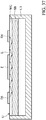
- FIG. 1 is an exploded diagram of a driving mechanism in accordance with an embodiment of the invention
- FIG. 2 is a perspective diagram of the driving mechanism in FIG. 1 after assembly
- FIG. 3 is a perspective diagram showing an optical system in the driving mechanism of FIGs. 1 and 2
- FIG. 4 is an exploded diagram of the spring sheet S, the optical element R1, and the mirror R2 in FIG. 3 .
- the driving mechanism in this embodiment is used to drive an optical element R1 (e.g. reflecting mirror) to rotate back and forth within a range, wherein the optical element R1 can reflect light to an object for the purpose of depth sensing or 3D scanning.
- an optical element R1 e.g. reflecting mirror
- the driving mechanism includes an upper module and a lower module.
- the lower module primarily comprises a base B, a light emitter D1 disposed on the base B, a light path adjusting element P, a circuit board C, and a light receiver D2 disposed on the circuit board C.
- the upper module primarily comprises a fixed member H, a spring sheet S, two magnets M, and two magnetic permeable sheets Q.
- the fixed member H is secured on the base B, and the spring sheet S, the magnets M, and the magnetic permeable sheets Q are disposed on the fixed member H.
- the fixed member H and the base B constitute a fixed part of the driving mechanism.
- the optical element R1 is disposed on a stage S3 of the spring sheet S, and they can rotate relative to the fixed member H to perform rapid depth sensing or 3D scanning of an object.
- the spring sheet S is used as a movable part of the driving mechanism, and it has two fixed ends S1 affixed to the fixed member H, two deformable portions S2, and a stage S3.
- the optical element R1 is disposed on the top side of the stage S3, and the deformable portions S2 respectively connecting the fixed ends S1 to the stage S3.
- a mirror R2 and at least one coil E2 are disposed on the bottom side of the stage S3 ( FIG. 3 ).
- the optical element R1 when an external light source (not shown) emits a sensing light L1 to the optical element R1 on the stage S3, the optical element R1 reflects the sensing light L1 to an object for depth sensing or 3D scanning. Additionally, the light emitter D1 in the lower module of the driving mechanism can emit another sensing light L2 to the light path adjusting element P (e.g. prism). The light path adjusting element P can guide the sensing light L2 to the mirror R2 on the bottom side of the stage S3, and the mirror R2 reflects the sensing light L2 to the light receiver D2, so as to obtain posture angle information of the optical element R1 relative to the fixed member H.
- the light path adjusting element P e.g. prism
- the light receiver D2 When the light receiver D2 receives the sensing light L2 that is reflected by the mirror R2, it can transmit an electrical signal to a processor via the circuit board C, whereby closed-loop rotational control for the stage S3 of the spring sheet S and the optical element R1 can be performed.
- the mirror R2 may be omitted from the driving mechanism, and the bottom surface of the stage S3 may be smooth or polished to reflect the sensing light L2.
- a through hole may be formed on the stage S3 for receiving the optical element R1 (e.g. double-sided mirror) without the mirror R2.
- the spring sheet S in this embodiment has a first resonance frequency with respect to the fixed part (the fixed member H and the base B), and an AC current signal can be applied to the coil E2 on the stage S3, wherein the frequency of the AC current signal corresponds to the first resonance frequency.
- the stage S3 can be driven to rapidly rotate back and forth within a range around the long axis A of the spring sheet S for depth sensing or 3D scanning of an object.
- the first resonance frequency is about 300-1000Hz
- the frequency of the AC current signal is about 0.9 to 1.1 times the first resonance frequency, so that the rotational angle of the stage S3 and the scanning range of the sensing light L1 can be increased.
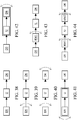
- FIG. 5 is a top view of the spring sheet S, the magnets M, and the magnetic permeable sheets Q in FIGs. 1 and 2
- FIG. 6 is a bottom view of the spring sheet S, the magnets M, and the magnetic permeable sheets Q in FIGs. 1 and 2
- the spring sheet S may comprise metal and have a rectangular structure.
- the magnets M and the magnetic permeable sheets Q are arranged on two long sides of the spring sheet S, and the circuit E1 and the coil E2 are respectively formed on the top and bottom sides of the spring sheet S by metallic printing ink or circuit-on-metal technology.
- the spring sheet S may comprise SUS 304H stainless steel that has high mechanical strength and reliability.
- the circuit E1 and the coil E2 can be integrally formed on the top and bottom sides of the spring sheet S, wherein an insulating layer is formed between the circuit E1 and the spring sheet S, and another insulating layer is formed between the coil E2 and the spring sheet S.
- the circuit E1 and the coil E2 can be electrically connected to each other via the stage S3 of the spring sheet S.
- an external circuit applies a current signal to the coil E2 on the bottom side of the spring sheet S via the circuit E1
- the magnet M and the coil E2 can produce a magnetic force to rotate the stage S3 around the long axis A of the spring sheet S, so as to perform depth sensing or 3D scanning of an object.
- the circuit E1 and the coil E2 in FIGs. 5-6 both have at least one segment parallel to the long axis A (first axis), and the segment at least partially overlaps the long axis A when viewed along the Z direction that is perpendicular to the spring sheet S.
- the circuit E1 and the coil E2 may also have a plurality of segments that are parallel to but do not overlap the long axis A when viewed along the Z direction.
- FIGs. 7 and 8 are exploded and perspective diagrams of a spring sheet S, an optical element R1, a mirror R2, two coils W, and a bobbin N, in accordance with another embodiment of the invention.
- FIG. 9 is a perspective diagram that shows the coils W in FIG. 8 electrically connecting to the circuits E3 on the spring sheet S.
- FIG. 10 is a perspective diagram of an optical system in accordance with another embodiment of the invention.
- this embodiment is different from FIGs. 1-6 in that a plurality of circuits E3 are integrally formed on the bottom side of the spring sheet S by metallic printing ink or circuit-on-metal technology, wherein an insulating layer is formed between the circuits E3 and the spring sheet S to prevent a short circuit therebetween.
- the two coils W in FIGs. 9-10 are respectively connected to the circuits E3 via the wires E, whereby an external circuit can transmit electrical signals to the coils W via the wires E and the circuits E3. It should be noted since two coils W are provided on the bottom side of the spring sheet S, the magnetic force for driving the stage S3 to rotate can be increased, and the range of depth sensing or 3D scanning can also be increased.
- FIGs. 11 and 12 are exploded and perspective diagrams of a light emitter D3, a light receiver D4, and a substrate I disposed on a spring sheet S, in accordance with another embodiment of the invention.
- FIG. 13 is a perspective diagram of an optical system in accordance with another embodiment of the invention.
- this embodiment is different from FIGs. 7-10 in that a light emitter D3, a light receiver D4, and a substrate I are disposed on a spring sheet S, and the optical element R1 shown in FIGs. 7-10 is omitted from the driving mechanism.
- FIG. 13 shows that the substrate I is disposed on the top side of the spring sheet S, and the light emitter D3 and the light receiver D4 are disposed on the substrate I, wherein an insulating layer is formed between the substrate I and the spring sheet S.
- the light emitter D3 and the light receiver D4 may respectively comprise laser diode and photo diode
- the substrate I may comprise a circuit board for electrically connecting the light emitter D3 and the light receiver D4 to an external circuit.
- the optical element R1 e.g. mirror
- the positioning accuracy during assembly and the performance of depth sensing or 3D scanning can be greatly increased.
- the production cost and the dimensions of the driving mechanism can also be reduced.
- only one of the light emitter D3 and the light receiver D4 is disposed on the spring sheet S, so that the circuits on the substrate I can be simplified.
- FIG. 14 is an exploded diagram of a spring sheet S, a coil W, and several magnets MX and MY, in accordance with another embodiment of the invention.
- FIG. 15 is a perspective diagram showing the spring sheet S, the coil W, and the magnets MX and MY in FIG. 14 assembled to a fixed member H.
- FIG. 16 is a perspective diagram showing the relative positions of the spring sheet S and the magnets MX and MY in FIG. 15 .
- the spring sheet S and the magnets MX and MY in this embodiment are affixed to the fixed member H, wherein the coil W can be integrally formed on the bottom side the spring sheet S by metallic printing ink or circuit-on-metal technology.
- the spring sheet S has two meandering deformable portions S2.
- the spring sheet S may have a first resonance frequency and a second resonance frequency with respect to the fixed member H, corresponding to the first and second axes AY and AX.
- a first AC current signal and a second AC current signal are sequentially applied to the coil W in a first time interval and a second time interval
- the stage S3 of the spring sheet S can be driven to rotate around the first and second axes AY and AX to perform depth sensing or 3D scanning of an object, wherein the frequencies of the first and second AC current signals correspond to the first and second resonance frequencies.
- the aforementioned driving mechanism may utilize the two coils W and the bobbin N in FIGs. 7-10 with the circuits E3 and wires E ( FIGs. 8-10 ).
- two different current signals can be individually applied to the two coils W, to drive the stage S3 and the optical element R1 (e.g. mirror) on the stage S3 to rotate around the first axis AY and the second axis AX at the same time.
- the second resonance frequency could be over 10 times the first resonance frequency.
- the stage S3 and the optical element R1 thereon can be driven to rotate around the first axis AY and the second axis AX at the same time by the coil W and the magnets MY and MX (driving assembly), thus greatly increasing the range of depth sensing or 3D scanning.
- FIGs. 17 is a perspective diagram showing the relative positions of a spring sheet S, at least one coil W, and several magnets M, in accordance with another embodiment of the invention.
- the spring sheet S in this embodiment has four fixed ends S1 affixed to the fixed part (the fixed member H and the base B), a stage S3 for carrying the optical element R1, and four deformable portions S2 connecting the four fixed ends S1 to the stage S3.
- four magnets M are affixed to the fixed part, and at least one coil W is affixed to the stage S3.
- an electrical current signal is applied to the coil W, a magnetic force can be produced to rotate the stage S3 back and forth within a range relative to the fixed part.
- the spring sheet S can define a rectangular area, and the four fixed ends S1 of the spring sheet S are located at the four corners of the rectangular area, so as to achieve miniaturization of the driving mechanism.
- FIG. 18 is a perspective diagram of a driving mechanism in accordance with an embodiment of the invention
- FIG. 19 is a perspective diagram of the two spring sheets S in FIG. 18
- this embodiment is different from FIGs. 1-2 in that the movable part includes two spring sheets S.
- Each of the spring sheet S that has a fixed end S1 secured on the fixed member H, a deformable portion S2, and a stage S3 for carrying the optical element R1.
- the stages S3 of the two spring sheets S are spaced apart from each other, and a bobbin N and two coils W are disposed on the bottom sides of the stages S3.
- the bobbin N is affixed to the stages S3, and the coils W are wound on the bobbin N.
- circuits E3 in FIG. 9 may be integrally formed on the stages S3 by metallic printing ink or circuit-on-metal technology to electrically connect to the two coils W.
- FIG. 20 is a perspective diagram of a spring sheet S in accordance with another embodiment of the invention.
- the movable part may comprise only one spring sheet S, and two sets of circuits E3 are integrally formed on the stages S3 of the spring sheet S by metallic printing ink or circuit-on-metal technology. It should be noted that the two sets of circuits E3 can be electrically connected to the two coils W, respectively. Moreover, an insulating layer K is formed between the circuits E3 and the spring sheet S to prevent short circuit therebetween.
- FIG. 21 is a partial sectional view showing a coil Y21 and a circuit Y31 formed on the same side of the spring sheet S.
- a multi-layer circuit structure can be formed on a surface of the spring sheet S to replace the bobbin N and the coil W in FIG. 18 .
- the coil Y21 and the circuit Y31 can be formed and stacked on the top side of the spring sheet S by metallic printing ink or circuit-on-metal technology, wherein the coil Y21 is located between the circuit Y31 and the spring sheet S.
- an insulating layer Y10 is formed between the coil Y21 and the spring sheet S, and two insulating structures Y20 and Y30 are formed around the coil Y21 and the circuit Y31 to prevent short circuit therebetween.
- FIG. 22 is a partial sectional view showing a coil Y21 and a circuit Y31 formed on the opposite sides of the spring sheet S.
- this embodiment is different from FIG. 21 in that the coil Y21 and the circuit Y31 are formed on the opposite sides of the spring sheet S, wherein an insulating layer Y10 is formed between the coil Y21 and the spring sheet S, and another layer Y10 is formed between the circuit Y31 and the spring sheet S.
- a multi-layer circuit structure can be formed on the spring sheet S to greatly reduce production cost and the thickness of the driving mechanism.
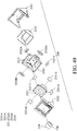
- FIGs. 23 and 24 are partial perspective view and top view of a driving mechanism in accordance with another embodiment of the invention.
- two spring sheet S are used as the movable part of the driving mechanism for sustaining a round optical element R1.
- a bobbin N and at least one coil W are affixed to the bottom side of the two spring sheet S, wherein the coil W is wound on the bobbin N.
- the bobbin N has a plurality of pins J (positioning structures), and at least one of the pins J extends through and protrudes from the top surface of the spring sheet S to contact and restrict the optical element R1 in a predetermined position, as shown in FIGs. 23 and 24 .
- the driving mechanism may further include a cover (not shown) to protect the spring sheets S and the optical element R1, and the stage S3 of the spring sheet S forms a protrusion S31 (positioning structure) protruding form a side of the spring sheet S, so as to restrict the cover can in a recess S32 adjacent to the protrusion S31.
- each spring sheet S forms two protrusions S31 that are symmetrical to the deformable portion S2, and the two recesses S32 are formed between the two protrusions S31 and the deformable portion S2.
- the spring sheet S in this embodiment forms at least one flat surface S33 (positioning structure) to contact and restrict the magnet M in a predetermined position in the X direction. Additionally, to enhance the connection strength between the spring sheet S and the bobbin N, the spring sheet S forms a bent portion S34 ( FIG. 23 ) bent toward the bobbin N, whereby the adhesion area between the spring sheet S and the bobbin N can be efficiently increased to prevent the bobbin N being separated from the spring sheet S.
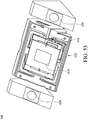
- FIG. 25 is a perspective diagram of a cover T in accordance with another embodiment of the invention
- FIG. 26 is a partial sectional view of the cover T in FIG. 25 , a fixed member H connected to the cover T, and two magnets M received in the cover T after assembly.
- the cover T in this embodiment is mounted to the fixed member H to protect the components therein.
- the cover T forms an opening T0, a plurality of pillars T1, and a plurality of protrusions T2, wherein the pillars T1 and the protrusions T2 are formed on the inner side of the cover T and extend in the -Z direction (vertical direction).
- each of the magnets M can be positioned in a space T11 ( FIG. 25 ) between two of the pillars T1, and the pillars T1 can restrict the magnets M to move in the Y direction (horizontal direction).
- the protrusions T2 on the inner side of the cover T can contact the magnets M in the -Z direction (vertical direction), so that the magnets M can be restricted in a predetermined position to prevent the magnets M being separated from the fixed member H.
- two magnetic permeable sheets Q may be embedded in the plastic fixed member H by insert molding. As the magnetic permeable sheets Q are located close to the magnets M, the magnets M can be rapidly and automatically attached to the surface of the fixed member H by magnetic attraction between the magnets M and the magnetic permeable sheets Q. Therefore, high positioning accuracy and efficient assembly of the driving mechanism can be achieved.
- FIG. 27 is a perspective diagram of an optical sensing system in accordance with an embodiment of the invention
- FIG. 28 is a perspective diagram of the optical module SM that changes the propagation direction of the sensing light L1 in FIG. 27 .
- the optical sensing system primarily comprises a light emitter TX, a light receiver RX, an optical module SM, and a focusing lens FL.
- the optical module SM includes a light path adjusting element PR and an optical element R1 ( FIG. 28 ).
- the optical element R1 and the light path adjusting element PR can be driven to respectively rotate around a first axis A1 and a second axis A2 within a range by a driving assembly (e.g. magnets and coils), so as to perform depth sensing or 3D scanning of an object O.
- a driving assembly e.g. magnets and coils
- the light emitter TX can emit a sensing light L1 to the optical module SM, and the light path adjusting element PR and the optical element R1 of the optical module SM can redirect the sensing light L1 to the object O. Subsequently, the sensing light L1 is reflected by the object O and propagates through the focusing lens FL to the light receiver RX.
- the light receiver RX can transfer light into an electrical signal and then transmit the electrical signal to a processor (not shown), so that 3D surface and depth information of the object O can be obtained.
- the optical element R1 in FIG. 28 is disposed on a stage S3 of the spring sheet S.
- the spring sheet S may comprise a round, oval or rectangular mirror, and any one of the driving mechanisms as disclosed in FIGs. 1-26 may be applied to the spring sheet S, so that the spring sheet S can be driven to rotate around a fist axis A1 within a first range.
- the light path adjusting element PR may comprise a prism that is movably connected to a fixed part (e.g. the base B and the fixed member H in FIGs. 1-2 ), and it can rotate around a second axis A2 relative to the fixed part, wherein the second axis A2 is not parallel to the first axis A1.
- the second axis A2 is perpendicular to the first axis A1.
- the sensing light L1 emitted from the light emitter TX propagates in an initial direction to the light path adjusting element PR, and the light path adjusting element PR redirects the sensing light L1 to propagate in an incident direction to the optical element R1 on the spring sheet S. Subsequently, the sensing light L1 is reflected by the optical element R1 to propagate in a reflecting direction and then reach the object O ( FIG. 27 ).
- the first axis A1 is perpendicular to the incident direction and the reflecting direction
- the second axis A2 is perpendicular to the initial direction and the incident direction.
- the optical element R1 and the light path adjusting element PR can respectively rotate around the first and second axes A1 and A2 back and forth for depth sensing or 3D scanning a surface of the object O.
- the optical element R1 and the stage S3 of the spring sheet S may be driven to rotate around the first axis A1 back and forth within a first range by open-loop control
- the light path adjusting element PR may be driven to rotate around the second axis A2 within a second range by closed-loop control.
- the spring sheet S has a first resonance frequency relative to the fixed part, and a first AC current signal can be applied to the coil of the driving assembly, thus driving the stage S3 to rotate around the first axis A1 back and forth within the first range.
- the light path adjusting element PR may be driven to rotate around the second axis A2 by a voice coil motor (VCM).
- VCM voice coil motor
- FIG. 29 is a perspective diagram of the sensing light L1 reflected by the optical element R1 to the object O while the light path adjusting element PR rotates around the second axis A2.
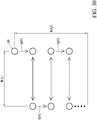
- FIG. 30 is a perspective diagram showing the optical element R1 continuously rotates around the first axis A1 back and forth within a first range RA1, and the light path adjusting element PR rotates around the second axis A2 within a second range RA2 in a stepwise manner.
- the sensing light L1 can scan through a fan-shaped area. Since the stage S3 of the spring sheet S can also rotate around the first axis A1 back and forth, the sensing light L1 can reach a specific surface area on the object O for depth sensing of 3D scanning.
- the optical element R1 and the stage S3 of the spring sheet S are driven to continuously rotate around the first axis A1 back and forth within the first range RA1.
- the light path adjusting element PR is driven to rotate in a stepwise manner around the second axis A2 within the second range RA2, different from the optical element R1 and the spring sheet S.
- the light path adjusting element PR rotates a first step angle SP1 in a predetermined direction around the second axis A2 from an initial position IP
- the light path adjusting element PR stops rotating around the second axis A2 temporarily.
- the light path adjusting element PR will rotate a second step angle SP2 again in the predetermined direction around the second axis A2 after the optical element R1 and the stage S3 of the spring sheet S rotates throughout the first range RA1.
- the light path adjusting element PR rotates the second step angle SP2 around the second axis A2 temporarily.
- the light path adjusting element PR will rotate a third step angle SP3 around the second axis A2 after the optical element R1 and the stage S3 of the spring sheet S rotates throughout the first range RA1, and so on.
- the sensing light L1 can be projected onto a surface area on the object O for depth sensing of 3D scanning.
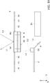
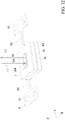
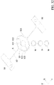
- FIG. 31 is a perspective diagram of an upper module of a driving mechanism in accordance with an embodiment of the invention.
- FIG. 32 is an exploded diagram of the spring sheet S, the coils W, and the bobbin N in FIG. 31 .
- the upper module in this embodiment is different from FIGs. 1-2 in that the longitudinal spring sheet S has two curved portions S21 and two bridge portions S22.
- the curved portions S21 respectively connects the deformable portions S2 to the round stage S3, and an opening is formed between the curved portions S21 and two bridge portions S22.
- FIG. 31 also shows that an optical element R1 and two coils W are respectively disposed on the top side and bottom side of the stage S3.
- two magnets M are arranged along the diagonal direction of the spring sheet S, and they have the same polar directions.
- FIG. 32 shows the bobbin N and two coils W (as disclosed in FIGs. 7-10 ) are disposed on the bottom side of the stage S3.
- the spring sheet S has a first resonance frequency and a second resonance frequency with respect to the fixed part.
- a first AC current signal can be applied to the coils W in a first time interval
- a second AC current signal can be applied to the coils W in a second time interval.
- the stage S3 can be driven to rotate back and forth around the long axis AL and the short axis AS of the spring sheet S in different time periods.
- the two coils W can also be energized by the first and second AC current signals at the same time.
- the stage S3 can be driven to rotate back and forth around the long axis AL and the short axis AS of the spring sheet S at the same time, wherein the long axis AL is perpendicular to the short axis AS.
- the first resonance frequency is from 10Hz to 30Hz
- the second resonance frequency is from 300Hz to 1000Hz, wherein the second resonance frequency may be over 10 times the first resonance frequency.
- the bobbin N can also be replaced by the multiple circuit structure as disclosed in FIGs. 21 and 22 , wherein the coil or the circuit may be integrally formed on top or bottom side of the spring sheet S by metallic printing ink or circuit-on-metal technology.
- the coil When the coil is energized by a current signal, the stage S3 of the spring sheet S can rotate around the long axis AL or the short axis AS.
- the circuit may be connected to a position sensor (e.g. Hall effect sensor) to obtain the posture angle of the stage S3 and the optical element R1.
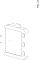
- FIG. 33 is a perspective diagram of a sensing module U and an analyzing device V
- FIG. 34 is a perspective diagram showing the sensing module U when connected to the analyzing device V.
- the sensing module U in this embodiment has a sensing film F.
- the sensing film F may comprise porous material to adsorb a specimen.
- the sensing module U can be inserted into a slot V0 on a side of the analyzing device V, so that the sensing module U and the analyzing device V are electrically connected to each other.
- a light source in the analyzing device V can project light onto the sensing module U for obtaining concentration or quantity information of the substance in the specimen.
- the sensing module U may comprise disposable material and is detachably connected to the analyzing device V. Hence, it could be easy to use and especially suitable in the field of point-of-care testing (POCT).
- POCT point-of-care testing
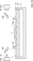
- FIG. 35 is a perspective diagram of an optical sensing system in accordance with an embodiment of the invention.
- a light emitter D5 can emit a sensing light L to a first optical coupler PM1 of the sensing module U, and the sensing light L then enters a light guide element WG under the first optical coupler PM1. Subsequently, the sensing light L is reflected multiple times within the light guide element WG and propagates into a second optical coupler PM2.
- a light receiver D6 in the analyzing device V finally receive the sensing light L and transfer the sensing light L into an electrical signal.
- the light receiver D6 can transmit sensing data to a processing unit (not shown) in the analyzing device V according to the sensing light L.
- the processing unit compares the sensing data with reference data in a memory unit and then transmits an image signal to the display V1.
- the sensing data includes intensity or phase information of the sensing light L.
- the light emitter D5, the light receiver D6, and the sensing module U can constitute an optical system, wherein the sensing module U has a hollow housing U1 and a substrate SB disposed in the housing U1.
- the light guide element WG is disposed on the substrate SN, and the sensing film F, the first optical coupler PM1, and the second optical coupler PM2 are all disposed on a top surface of the light guide element WG.
- the light guide element WG may be an optical waveguide (OWG) that comprises polymer resin, and the substrate SB may comprise quartz or glass.
- the light emitter D5 may comprise an LED or LD, the light receiver D6 may comprise photodiode, and the sensing light L may be laser or general light.
- the first and second optical couplers PM1 and PM2 may comprise prisms or other optical lenses, and the sensing film F is located between the first and second optical couplers PM1 and PM2.
- the sensing light L propagates through the first optical coupler PM1 into the light guide element WG, the sensing light L is reflected multiple times inside the light guide element WG, and an evanescent wave of the sensing light L can cause Surface Plasmon Resonance (SPR) between the light guide element WG and the sensing film F.
- SPR Surface Plasmon Resonance
- the intensity or phase of the sensing light L received by the light receiver D6 would be different from the sensing light L generated by the light emitter D5, whereby the concentration or quantity of the specific substance in the specimen can be determined.
- the specific substance may comprise glucose or anti-allergen antibody.
- a driving mechanism DM1 in the analyzing device V is provided and connected to the light emitter D5.
- the driving mechanism DM1 can drive the light emitter D5 to rotate relative to the sensing module U, to ensure the sensing light L emitted by the light emitter D5 can successfully and efficiently propagate through the first optical coupler PM1 to the light guide element WG.
- another driving mechanism DM2 in this embodiment is provided and connected to the light receiver D6 for driving the light receiver D6 to rotate relative to the sensing module U, thus ensuring the sensing light L that propagates through the second optical coupler PM2 can efficiently and successfully reach the light receiver D6.
- the driving mechanisms DM1 and DM2 may comprise a voice coil motor (VCM) that applies the configuration of the driving mechanisms as disclosed in FIGs. 1-32 , so that the angle of the light emitter D5 and the light receiver D6 can be appropriately adjusted to improve the efficiency of the optical sensing system.
- VCM voice coil motor
- FIG. 36 is a perspective diagram of an optical sensing system in accordance with another embodiment of the invention. As shown in FIG. 36 , this embodiment is different from FIG. 35 in that a first light path adjusting element RM1 and a second light path adjusting element RM2 are provided in the analyzing device V to guide the sensing light L into/out of the sensing module U.
- a first light path adjusting element RM1 and a second light path adjusting element RM2 are provided in the analyzing device V to guide the sensing light L into/out of the sensing module U.
- the light emitter D5 emits the sensing light L to the first light path adjusting element RM1, and the first light path adjusting element RM1 redirects the sensing light L to propagate through the first optical coupler PM1 and into the light guide element WG. Subsequently, the sensing light L propagates through the light guide element WG and the second optical coupler PM2 to the second light path adjusting element RM2, and the second light path adjusting element RM2 guides the sensing light L to the light receiver D6.
- the light emitter D5 and the first optical coupler PM1 (or the light receiver D6 and the second light path adjusting element RM2, or the light emitter D5, the light receiver D6 and the first and second light path adjusting element RM1 and RM2) are arranged in a direction parallel to the light guide element WG for miniaturization of the optical sensing system.
- the first and second light path adjusting element RM1 and RM2 may comprise a prism or mirror that has a curved surface, and they may apply the configuration of the driving mechanisms as disclosed in FIGs. 1-32 , so that they can be appropriately driven to rotate and efficiently guide the sensing light L to the light receiver D6.
- FIG. 37 is a perspective diagram of an optical sensing system in accordance with another embodiment of the invention. As shown in FIG. 37 , this embodiment is different from FIG. 35 in that the first and second optical couplers PM1 and PM2 are omitted from the optical sensing system.
- the light emitter D5 and the light receiver D6 are directly disposed on the top surface of the light guide element WG.
- the light receiver D6 may have a thickness larger than the light emitter D5 to efficiently receive the sensing light L and facilitate miniaturization of the optical sensing system.
- the light emitter D5 may comprise OLED
- the light receiver D6 may comprise organic photodiodes (OPD), and both of them are directly formed on the top surface of the light guide element WG by a coating process.
- OPD organic photodiodes
- the sensing light L can directly enters the light guide element WG and prevent the positioning error between the light emitter D5 and the light guide element WG.
- a middle layer (not shown) may be formed between the light guide element WG and the light receiver D6, wherein the middle layer comprises a refractive index greater than the light guide element WG or ranged between the light guide element WG and the light receiver D6.
- the middle layer may be integrally formed with the light receiver D6 in one piece.
- FIG. 38 is a perspective diagram showing the sensing light L propagates from the light emitter D5 through the sensing module U to the light receiver D6.
- FIG. 39 is a perspective diagram showing the light emitter D5 is rotatable relative to the sensing module U.
- FIG. 40 is a perspective diagram showing the light emitter D5 and the light receiver D6 are both rotatable relative to the sensing module U.
- the sensing light L is emitted from the light emitter D5 through the sensing module U to the light receiver D6, wherein the light emitter D5 and the light receiver D6 may be disposed inside the analyzing device V or directly affixed to the light guide element WG of the sensing module U ( FIG. 37 ).
- the light emitter D5 may be rotatable relative to the sensing module U by applying the driving mechanism DM1 in FIGs. 35 and 36 , so that the sensing light L can be successfully and efficiently guided into the light guide element WG.
- the light emitter D5 and the light receiver D6 are both rotatable relative to the sensing module U by applying the driving mechanisms DM1 and DM2 in FIGs. 35 and 36 , so that the light receiver D6 can efficiently receive the sensing light L.
- FIG. 41 is a perspective diagram showing the light emitter D5 and the sensing module U are rotatable relative to the light receiver D6.
- FIG. 42 is a perspective diagram showing the light receiver D6 and the sensing module U are rotatable relative to the light emitter D5.
- the light emitter D5 may be affixed to the sensing module U, and they can both rotate relative to the light receiver D6 by applying the driving mechanisms as disclosed in FIGs. 1-32 , so that light receiver D6 can efficiently receive the sensing light L.
- the light receiver D6 may be affixed to the sensing module U, and they can both rotate relative to the light emitter D5 by applying the driving mechanisms as disclosed in FIGs. 1-32 , so that the sensing light L can be successfully and efficiently guided to the sensing module U.
- FIG. 43 is a perspective diagram showing the first light path adjusting element RM1 is rotatable relative to the sensing module U.
- FIG. 44 is a perspective diagram showing the first and second light path adjusting elements RM1 and RM2 are both rotatable relative to the sensing module U.
- the first light path adjusting element RM1 may be disposed in the analyzing device V for guiding the sensing light L to the sensing module U ( FIG. 36 ). Specifically, the first light path adjusting element RM1 can rotate relative to the sensing module U or the light emitter D5.
- the second light path adjusting element RM2 may also be disposed in the analyzing device V for guiding the sensing light L to the light receiver D6, so that the light receiver D6 can efficiently receive the sensing light L.
- the sensing module U may comprise disposable material and is detachably connected to the analyzing device V. Hence, it could be easy to use and especially suitable in the field of point-of-care testing (POCT).
- POCT point-of-care testing
- Fig. 45 is a schematic diagram of an optical member driving mechanism 100
- Fig. 46 is an exploded-view diagram of the optical member driving mechanism 100.
- the optical member driving mechanism 100 can be mounted in a vehicle (such as a car or a motorcycle) or a portable device (such as a smart phone or a tablet computer), and can be electrically connected to a processer (not shown).
- the optical member driving mechanism 100 can emit light toward an object, and receive the light reflected by the object.
- the processor can calculate the profile of the object according to the time lag between emitting and receiving, or the data of luminous intensity of the received light.
- the optical member driving mechanism 100 primarily includes a light emitter 110, a light receiver 120, and a rotation module 130, wherein the light emitter 110 and the light receiver 120 are disposed on the rotation module 130.
- the light emitter 110 emits light toward a direction away from the optical member driving mechanism 100 at a side 101 of the optical member driving mechanism 100, and the light receiver 120 receives the same type light being emitted toward the optical member driving mechanism 100 at the same side 101.
- the light can be an infrared light, a white light, or a laser.
- the rotation module 130 includes a fixed portion 131, a movable portion 132, and a driving assembly 133.
- the fixed portion 131 can be a base, and the movable portion 132 can be a carrier.
- the movable portion 132 is movably connected to the fixed portion 131.
- the movable portion 132 has a metal substrate 1321, an insulation layer 1322, and a wire layer 1323.
- the insulation layer 1322 is disposed between the metal substrate and the wire layer 1323.
- the light emitter 110 and the light receiver 120 are disposed on the insulation layer 1322 and electrically connected to the wire layer 1323.
- the metal substrate 1321 is constituted by a flexible sheet spring, including at least one first engaged section 1321A, at least one second engaged section 1321B, and at least one string section 1321C.
- the first engaged section 1321A is affixed to the fixed portion 131
- the insulation layer 1322 is disposed on the second engaged section 1321B
- the string section 1321C connects the first engaged section 1321A to the second engaged section 1321B. Therefore, the light emitter 110 and the light receiver 120 can be suspended on the fixed portion 131 by the metal substrate 1321 of the movable portion 132.
- the driving assembly 133 includes at least one first electromagnetic driving member 1331, at least one second electromagnetic driving member 1332, and at least one magnetic permeability member 1333.
- the first electromagnetic driving member 1331 is disposed on the fixed portion 131.
- the second electromagnetic driving member 1332 is disposed on the movable portion and corresponds to the first electromagnetic driving member 1331.
- the second engaged section 1321B can be driven to move relative to the fixed portion 131 by the first electromagnetic driving member 1331 and the second electromagnetic driving member 1332.
- the first electromagnetic member 1331 is a magnet
- the second electromagnetic member 1332 is a coil.
- an electromagnetic effect is generated between the first electromagnetic driving member 1331 and the second electromagnetic member 1332, and the second engaged section 1321B is driven to rotate around a first rotation axis 11 relative to the fixed portion 131.
- the magnetic permeability member 1333 is adjacent to the first electromagnetic member 1331 to enhance the magnetic pushing force.
- the first electromagnetic member 1331 is a coil
- the second electromagnetic member 1332 is a magnet.
- the light emitter 110 and the light receiver 120 are disposed on the second engaged section 1321B, when the second engaged section 1321B is driven to rotate, the light emitter 110 and the light receiver 120 rotate simultaneously. Therefore, the scanning range of the optical member driving mechanism 100 can be increased, and the situation that the reflected light cannot be received by the light receiver 120 due to the position can be reduced.
- the insulation layer 1322 and the second electromagnetic driving member 1332 are respectively disposed on opposite sides of the metal substrate 1321. Furthermore, the light emitter 110 and the light receiver 120 are arranged along the first rotation axis 11, so that the first rotation axis 11 passes through the light emitter 110 and the light receiver 120. In some embodiments, the light emitter 110 and the light receiver 120 are respectively disposed on the different sides of the first rotation axis 11, and the distance between the light emitter 110 and the first rotation axis 11 is substantially the same as the distance between the light receiver 120 and the first rotation axis 11.
- an optical member driving mechanism 200 primarily includes a light emitter 210, a light receiver 220, and a rotation module.
- the light emitter 210 and the light receiver 220 are disposed on the rotation module 230, and the rotation module 230 can drive the light emitter 210 and the light receiver 220 to rotate around a first rotation axis 21 and a second rotation axis 22, wherein the first rotation axis 21 is perpendicular to the second rotation axis 22.
- the rotation module 230 includes a fixed portion 231, a movable portion 232, and a driving assembly 233.
- the fixed portion 231 includes a base 2311 and a frame 2312.
- the base 2311 is fixedly joined to the frame 2312.
- the movable portion 232 includes a supporting member 2321 and a carrier 2322.
- the movable portion 232 is movably connected to the fixed portion 231.
- the carrier 2322 has a metal substrate 2324, an insulation layer 2325, and a wire layer 2326.
- the insulation layer 2325 is disposed between the metal substrate 2324 and the wire layer 2326.
- the light emitter 210 and the light receiver 220 are disposed on the insulation layer 2325 and electrically connected to the wire layer 2326.
- the metal substrate 2324 is constituted by a flexible sheet spring, including at least one first engaged section 2324A, at least one second engaged section 2324B, and at least one string section 2324C.
- the first engaged section 2324A is affixed to the frame 2312
- the insulation layer 2325 is disposed on the second engaged section 2324B
- the string section 2324C connects the first engaged section 2324A to the second engaged section 2324B. Therefore, the light emitter 210 and the light receiver 220 can be suspended on the fixed portion 231 by the metal substrate 2324 of the movable portion 232.
- the supporting member 2321 is connected to the second engaged section 2324B, and the second engaged section 2324B is disposed between the supporting member 2321 and the insulation layer 2325.
- the driving assembly 233 includes at least one first electromagnetic driving member 2331A, at least one first electromagnetic driving member 2331B, at least one second electromagnetic driving member 2332A, at least one second electromagnetic driving member 2332B, and a circuit board 2333.
- the first electromagnetic driving members 2331A and 2331B are affixed to the supporting member 2321, and respectively disposed on the different surfaces of the supporting member 2321.
- the circuit board 2333 is clamped between the base 2311 and the frame 2312.
- the second electromagnetic driving members 2332A and 2332B are disposed on the circuit board 2333, and respectively corresponds the first electromagnetic driving members 2331A and 2331B through the openings 2313 of the frame 2312.
- the second engaged section 2324B can be driven to move relative to the fixed portion 231 by the first electromagnetic driving members 2331A and 2331B and the second electromagnetic driving members 2332A and 2332B.
- the first electromagnetic members 2331A and 2331B are magnets
- the second electromagnetic members 2332A and 2332B are coils.
- a current flows through the second electromagnetic member 2332A an electromagnetic effect is generated between the first electromagnetic driving member 2331A and the second electromagnetic member 2332A, and the second engaged section 2324B is driven to rotate around the first rotation axis 21 relative to the fixed portion 231.
- a current flows through the second electromagnetic member 2332B an electromagnetic effect is generated between the first electromagnetic driving member 2331B and the second electromagnetic member 2332B, and the second engaged section 2324B is driven to rotate around the second rotation axis 22 relative to the fixed portion 231.
- the light emitter 210 and the light receiver 220 are disposed on the second engaged section 2324B, when the second engaged section 2324B is driven to rotate, the light emitter 210 and the light receiver 220 rotate simultaneously. Therefore, the scanning range of the optical member driving mechanism 200 can be increased, and the situation that the reflected light cannot be received by the light receiver 220 due to the position can be reduced.
- the light emitter 210 and the light receiver 220 are arranged along the first rotation axis 21, so that the first rotation axis 21 passes through the light emitter 210 and the light receiver 220. Moreover, the light emitter 210 and the light receiver 220 are respectively disposed on the different sides of the second rotation axis 22, and the distance between the light emitter 210 and the second rotation axis 22 is substantially the same as the distance between the light receiver 220 and the second rotation axis 22.
- an optical member driving mechanism 300 primarily includes two light emitters 310, a light receiver 320, and a rotation module 330, wherein the structure of the rotation module 330 is the same as that of the rotation module 230, so that the features thereof are not repeated in the interest of brevity.
- the light receiver 320 is disposed on the movable portion 332 of the rotation module 330, and two light emitters 310 are disposed on opposite sides of the light receiver 320. Owing to the rotation of the light receiver 320, the scanning range of the optical member driving mechanism 300 can be increased. Furthermore, since the light receiver 320 can receive the reflected lights from two light emitters 310, the profile of the object can be accurately calculated.
- an optical member driving mechanism 400 primarily includes a light emitter 410, two light receivers 420, and a rotation module 430, wherein the structure of the rotation module 430 is the same as that of the rotation module 230, so that the features thereof are not repeated in the interest of brevity.
- the light emitter 410 is disposed on the movable portion 432 of the rotation module 430, and two light receivers 420 are disposed on opposite sides of the light emitter 410.
- the light receiving ranges of two light receivers 420 can be overlapped. Owing to the rotation of the light emitter 410, the scanning range of the optical member driving mechanism 400 can be increased.
- an optical member driving mechanism 500 primarily includes a light emitter 510, two light receivers 520, a rotation module 530, and a reflecting member 540, wherein the structure of the rotation module 530 is the same as that of the rotation module 230, so that the features thereof are not repeated in the interest of brevity.
- the reflecting member 540 can be a mirror or a prism, and can be disposed on the rotation module 530.
- the light emitter 510 emits light 1000 toward the reflecting member 540. After being reflected by the reflecting member 540, the light 1000 moves toward the object in a particular direction 1001.
- Two light receivers 520 are disposed on opposite sides of the reflecting member 540. After being reflected by the object, the light 1000 can be received by two receivers 520.
- the light emitter 510 overlaps one of the light receivers 520, so as to save space.
- the optical member driving mechanism 500 in this embodiment can be used in the vehicle, so as to save space between two receivers 520 to dispose other components.
- an optical member driving mechanism 600 primarily includes a light emitter 610, a light receiver 620, a rotation module 630, and a reflecting member 640, wherein the structure of the rotation module 630 is the same as that of the rotation module 230, so that the features thereof are not repeated in the interest of brevity.
- the reflecting member 640 can be a mirror or a prism, and can be disposed on the rotation module 630.
- the light emitter 610 emits light 1000 toward the reflecting member 640, and the reflecting member 640 reflects the light 1000 to the object. After being reflected by the object, the light 1000 can be received by the receiver 620.
- the light emitter 610, the reflecting member 640, and the light receiver 620 are arranged in a straight line 1002, so that the thickness of the optical member driving mechanism 600 can be reduced.
- the optical member driving mechanism 600 can be used in the portable device.
- the emission direction 1001 of the reflected light 1000 can be parallel or perpendicular to the second rotation axis 22.
- the light being emitting toward the object can shift horizontally.
- the direction of the magnetic pushing force of the driving assembly 233 can be changed to adjust the second rotation axis 22.
- the second rotation axis 22 can be adjusted to be parallel or perpendicular to the emission direction 1001 of the reflected light 1000, so that the light being emitted toward the object can shift horizontally.
- the light emitter and the light receiver can be a fill light member (such as a flash) and an image sensor.
- an optical member driving mechanism including a movable portion, a fixed portion, a driving assembly, at least one light emitter, and at least one light receiver.
- the driving assembly is configured to drive the movable portion to move relative to the fixed portion.
- the light emitter emits light toward an object, and the light receiver receives the light reflected by the object.
Landscapes
- Physics & Mathematics (AREA)
- Engineering & Computer Science (AREA)
- General Physics & Mathematics (AREA)
- Remote Sensing (AREA)
- Computer Networks & Wireless Communication (AREA)
- Radar, Positioning & Navigation (AREA)
- Optics & Photonics (AREA)
- Electromagnetism (AREA)
- Chemical & Material Sciences (AREA)
- Combustion & Propulsion (AREA)
- Power Engineering (AREA)
- Mechanical Light Control Or Optical Switches (AREA)
- Optical Radar Systems And Details Thereof (AREA)
- Mounting And Adjusting Of Optical Elements (AREA)
Priority Applications (14)
| Application Number | Priority Date | Filing Date | Title |
|---|---|---|---|
| CN201911365937.8A CN111381328B (zh) | 2018-12-27 | 2019-12-26 | 驱动机构 |
| CN202310776592.5A CN116679412A (zh) | 2018-12-27 | 2019-12-26 | 驱动机构 |
| CN202310777169.7A CN116819493A (zh) | 2018-12-27 | 2019-12-26 | 光学组件驱动机构 |
| CN201922387810.8U CN211348751U (zh) | 2018-12-27 | 2019-12-26 | 驱动机构 |
| CN202310777241.6A CN116794796A (zh) | 2018-12-27 | 2019-12-26 | 驱动机构 |
| US16/728,683 US11366278B2 (en) | 2018-12-27 | 2019-12-27 | Optical member driving mechanism |
| US16/728,734 US11686919B2 (en) | 2018-12-27 | 2019-12-27 | Driving mechanism |
| CN201922393570.2U CN211205207U (zh) | 2018-12-27 | 2019-12-27 | 光学组件驱动机构 |
| US16/738,510 US11422334B2 (en) | 2019-02-25 | 2020-01-09 | Driving mechanism |
| US16/738,486 US11693208B2 (en) | 2019-02-01 | 2020-01-09 | Optical sensing system |
| US16/738,547 US11300761B2 (en) | 2019-08-30 | 2020-01-09 | Driving mechanism |
| CN202020132568.XU CN211698371U (zh) | 2019-08-30 | 2020-01-20 | 驱动机构 |
| CN202020149548.3U CN212391611U (zh) | 2019-02-01 | 2020-02-01 | 光学感测系统 |
| CN202020199347.4U CN211955984U (zh) | 2019-02-25 | 2020-02-24 | 驱动机构 |
Applications Claiming Priority (4)
| Application Number | Priority Date | Filing Date | Title |
|---|---|---|---|
| US201862785593P | 2018-12-27 | 2018-12-27 | |
| US201962799886P | 2019-02-01 | 2019-02-01 | |
| US201962809891P | 2019-02-25 | 2019-02-25 | |
| US201962894295P | 2019-08-30 | 2019-08-30 |
Publications (3)
| Publication Number | Publication Date |
|---|---|
| EP3674769A2 true EP3674769A2 (de) | 2020-07-01 |
| EP3674769A3 EP3674769A3 (de) | 2020-09-16 |
| EP3674769B1 EP3674769B1 (de) | 2025-06-04 |
Family
ID=68916455
Family Applications (1)
| Application Number | Title | Priority Date | Filing Date |
|---|---|---|---|
| EP19218906.6A Active EP3674769B1 (de) | 2018-12-27 | 2019-12-20 | Antrieb |
Country Status (3)
| Country | Link |
|---|---|
| US (1) | US11686919B2 (de) |
| EP (1) | EP3674769B1 (de) |
| CN (5) | CN211348751U (de) |
Cited By (1)
| Publication number | Priority date | Publication date | Assignee | Title |
|---|---|---|---|---|
| EP3876018A3 (de) * | 2020-03-06 | 2021-12-29 | Tdk Taiwan Corp. | Mechanismus zur ansteuerung eines optischen elements |
Families Citing this family (6)
| Publication number | Priority date | Publication date | Assignee | Title |
|---|---|---|---|---|
| EP3674769B1 (de) * | 2018-12-27 | 2025-06-04 | Tdk Taiwan Corp. | Antrieb |
| CN111856698A (zh) * | 2020-08-19 | 2020-10-30 | 新思考电机有限公司 | 驱动结构、驱动装置及电子设备 |
| CN111856695A (zh) * | 2020-08-19 | 2020-10-30 | 新思考电机有限公司 | 驱动机构、驱动装置及电子设备 |
| CN115016085B (zh) * | 2021-02-19 | 2026-01-27 | 台湾东电化股份有限公司 | 光学元件驱动机构 |
| CN216748233U (zh) * | 2021-03-05 | 2022-06-14 | 台湾东电化股份有限公司 | 光学元件驱动机构 |
| US20230204829A1 (en) * | 2021-12-27 | 2023-06-29 | Tdk Taiwan Corp. | Optical element driving mechanism |
Family Cites Families (19)
| Publication number | Priority date | Publication date | Assignee | Title |
|---|---|---|---|---|
| JP2821581B2 (ja) * | 1990-10-16 | 1998-11-05 | キヤノン株式会社 | トラッキング用回動ミラー装置 |
| US5268784A (en) * | 1991-02-05 | 1993-12-07 | Canon Kabushiki Kaisha | Pivotable mirror device for tracking |
| JPH07296406A (ja) * | 1994-04-21 | 1995-11-10 | Matsushita Electric Ind Co Ltd | ミラー駆動装置 |
| JPH09211373A (ja) * | 1996-02-02 | 1997-08-15 | Asahi Optical Co Ltd | 走査光学装置 |
| JP3500044B2 (ja) * | 1997-06-27 | 2004-02-23 | ペンタックス株式会社 | ガルバノミラー装置 |
| JP4301688B2 (ja) * | 2000-03-28 | 2009-07-22 | 日本信号株式会社 | プレーナー型ガルバノミラー及びその製造方法 |
| JP4680373B2 (ja) * | 2000-11-16 | 2011-05-11 | オリンパス株式会社 | ガルバノミラー |
| JP2004240140A (ja) * | 2003-02-05 | 2004-08-26 | Olympus Corp | 光学素子保持機構 |
| JP2006201306A (ja) * | 2005-01-18 | 2006-08-03 | Pentax Corp | ステージ装置及びこのステージ装置を利用したカメラの手振れ補正装置 |
| JP2008281339A (ja) * | 2006-04-26 | 2008-11-20 | Sanyo Electric Co Ltd | レーザレーダ用駆動装置 |
| EP2101214A1 (de) * | 2008-03-13 | 2009-09-16 | Tdk Taiwan Corp. | EMI-geprüfter Miniaturlinsen-Fokussiermechanismus |
| KR101090961B1 (ko) * | 2010-03-24 | 2011-12-08 | 광주과학기술원 | 광 스캐너 및 광 스캐너 제조 방법 |
| JP5622443B2 (ja) * | 2010-06-08 | 2014-11-12 | 日本電産サンキョー株式会社 | 振れ補正機能付き光学ユニット |
| JP5842467B2 (ja) * | 2010-11-16 | 2016-01-13 | 株式会社リコー | アクチュエータ装置、このアクチュエータ装置用の保護カバー、このアクチュエータの製造方法、このアクチュエータ装置を用いた光偏向装置、二次元光走査装置及びこれを用いた画像投影装置 |
| JP6260019B2 (ja) * | 2012-11-09 | 2018-01-17 | 北陽電機株式会社 | 金属弾性部材、微小機械装置、微小機械装置の製造方法、揺動制御装置及び揺動制御方法 |
| JP6069628B2 (ja) * | 2012-12-03 | 2017-02-01 | 北陽電機株式会社 | 偏向装置、光走査装置及び走査式測距装置 |
| WO2018176277A1 (zh) * | 2017-03-29 | 2018-10-04 | 深圳市大疆创新科技有限公司 | 激光测量装置和移动平台 |
| US11340418B2 (en) * | 2018-12-27 | 2022-05-24 | Tdk Taiwan Corp. | Optical member driving mechanism |
| EP3674769B1 (de) * | 2018-12-27 | 2025-06-04 | Tdk Taiwan Corp. | Antrieb |
-
2019
- 2019-12-20 EP EP19218906.6A patent/EP3674769B1/de active Active
- 2019-12-26 CN CN201922387810.8U patent/CN211348751U/zh active Active
- 2019-12-26 CN CN202310776592.5A patent/CN116679412A/zh active Pending
- 2019-12-26 CN CN202310777169.7A patent/CN116819493A/zh active Pending
- 2019-12-26 CN CN202310777241.6A patent/CN116794796A/zh active Pending
- 2019-12-26 CN CN201911365937.8A patent/CN111381328B/zh active Active
- 2019-12-27 US US16/728,734 patent/US11686919B2/en active Active
Cited By (1)
| Publication number | Priority date | Publication date | Assignee | Title |
|---|---|---|---|---|
| EP3876018A3 (de) * | 2020-03-06 | 2021-12-29 | Tdk Taiwan Corp. | Mechanismus zur ansteuerung eines optischen elements |
Also Published As
| Publication number | Publication date |
|---|---|
| CN116679412A (zh) | 2023-09-01 |
| CN111381328B (zh) | 2023-07-18 |
| CN211348751U (zh) | 2020-08-25 |
| US20200209520A1 (en) | 2020-07-02 |
| CN116794796A (zh) | 2023-09-22 |
| US11686919B2 (en) | 2023-06-27 |
| CN116819493A (zh) | 2023-09-29 |
| EP3674769B1 (de) | 2025-06-04 |
| EP3674769A3 (de) | 2020-09-16 |
| CN111381328A (zh) | 2020-07-07 |
Similar Documents
| Publication | Publication Date | Title |
|---|---|---|
| US11693208B2 (en) | Optical sensing system | |
| EP3674769A2 (de) | Antrieb | |
| US11300761B2 (en) | Driving mechanism | |
| US20200209612A1 (en) | Optical member driving mechanism | |
| US20120242622A1 (en) | Touch module | |
| US11422334B2 (en) | Driving mechanism | |
| CN107544111B (zh) | 面状照明装置 | |
| CN103460126A (zh) | 带抖动修正功能的光学单元 | |
| JP6070349B2 (ja) | 接合装置及び接合方法 | |
| CN208386725U (zh) | 电子设备 | |
| JP6303972B2 (ja) | 面光源装置、表示装置、及び電子機器 | |
| WO2020088081A1 (zh) | 背光模块及其制作方法、液晶显示装置 | |
| CN211349378U (zh) | 屏下指纹识别装置及电子设备 | |
| KR20250001827A (ko) | 카메라 모듈 및 그를 포함하는 전자 장치 | |
| CN216792494U (zh) | 导光构件和显示装置 | |
| JP4032245B2 (ja) | 光通信システムおよび電子機器 | |
| CN114815120A (zh) | 发射模组、取像模组及电子设备 | |
| WO2015194360A1 (ja) | 光学式センサ | |
| CN115508945B (zh) | 导光构件、显示装置和用于制造显示装置的方法 | |
| KR102638695B1 (ko) | 렌즈 구동 장치, 광출력 모듈 및 라이다 | |
| JP2010256884A (ja) | 光導波路及び光配線部材並びに光配線部材への光素子の実装方法 | |
| CN117292621A (zh) | 一种显示装置 | |
| JP4849505B2 (ja) | 位置検出装置、該位置検出装置を有する光学装置 | |
| CN119575734A (zh) | 灯光组件和电子设备 | |
| CN116452968A (zh) | 一种摄像模组的组装系统及其组装方法 |
Legal Events
| Date | Code | Title | Description |
|---|---|---|---|
| PUAI | Public reference made under article 153(3) epc to a published international application that has entered the european phase |
Free format text: ORIGINAL CODE: 0009012 |
|
| STAA | Information on the status of an ep patent application or granted ep patent |
Free format text: STATUS: THE APPLICATION HAS BEEN PUBLISHED |
|
| AK | Designated contracting states |
Kind code of ref document: A2 Designated state(s): AL AT BE BG CH CY CZ DE DK EE ES FI FR GB GR HR HU IE IS IT LI LT LU LV MC MK MT NL NO PL PT RO RS SE SI SK SM TR |
|
| AX | Request for extension of the european patent |
Extension state: BA ME |
|
| PUAL | Search report despatched |
Free format text: ORIGINAL CODE: 0009013 |
|
| AK | Designated contracting states |
Kind code of ref document: A3 Designated state(s): AL AT BE BG CH CY CZ DE DK EE ES FI FR GB GR HR HU IE IS IT LI LT LU LV MC MK MT NL NO PL PT RO RS SE SI SK SM TR |
|
| AX | Request for extension of the european patent |
Extension state: BA ME |
|
| RIC1 | Information provided on ipc code assigned before grant |
Ipc: G02B 13/00 20060101ALI20200811BHEP Ipc: G02B 7/182 20060101AFI20200811BHEP |
|
| STAA | Information on the status of an ep patent application or granted ep patent |
Free format text: STATUS: REQUEST FOR EXAMINATION WAS MADE |
|
| STAA | Information on the status of an ep patent application or granted ep patent |
Free format text: STATUS: EXAMINATION IS IN PROGRESS |
|
| 17P | Request for examination filed |
Effective date: 20210316 |
|
| RBV | Designated contracting states (corrected) |
Designated state(s): AL AT BE BG CH CY CZ DE DK EE ES FI FR GB GR HR HU IE IS IT LI LT LU LV MC MK MT NL NO PL PT RO RS SE SI SK SM TR |
|
| 17Q | First examination report despatched |
Effective date: 20210415 |
|
| GRAP | Despatch of communication of intention to grant a patent |
Free format text: ORIGINAL CODE: EPIDOSNIGR1 |
|
| STAA | Information on the status of an ep patent application or granted ep patent |
Free format text: STATUS: GRANT OF PATENT IS INTENDED |
|
| INTG | Intention to grant announced |
Effective date: 20250131 |
|
| GRAS | Grant fee paid |
Free format text: ORIGINAL CODE: EPIDOSNIGR3 |
|
| GRAA | (expected) grant |
Free format text: ORIGINAL CODE: 0009210 |
|
| STAA | Information on the status of an ep patent application or granted ep patent |
Free format text: STATUS: THE PATENT HAS BEEN GRANTED |
|
| AK | Designated contracting states |
Kind code of ref document: B1 Designated state(s): AL AT BE BG CH CY CZ DE DK EE ES FI FR GB GR HR HU IE IS IT LI LT LU LV MC MK MT NL NO PL PT RO RS SE SI SK SM TR |
|
| REG | Reference to a national code |
Ref country code: GB Ref legal event code: FG4D |
|
| REG | Reference to a national code |
Ref country code: CH Ref legal event code: EP |
|
| REG | Reference to a national code |
Ref country code: DE Ref legal event code: R096 Ref document number: 602019070705 Country of ref document: DE |
|
| REG | Reference to a national code |
Ref country code: IE Ref legal event code: FG4D |
|
| REG | Reference to a national code |
Ref country code: NL Ref legal event code: MP Effective date: 20250604 |
|
| PG25 | Lapsed in a contracting state [announced via postgrant information from national office to epo] |
Ref country code: FI Free format text: LAPSE BECAUSE OF FAILURE TO SUBMIT A TRANSLATION OF THE DESCRIPTION OR TO PAY THE FEE WITHIN THE PRESCRIBED TIME-LIMIT Effective date: 20250604 Ref country code: ES Free format text: LAPSE BECAUSE OF FAILURE TO SUBMIT A TRANSLATION OF THE DESCRIPTION OR TO PAY THE FEE WITHIN THE PRESCRIBED TIME-LIMIT Effective date: 20250604 |
|
| REG | Reference to a national code |
Ref country code: LT Ref legal event code: MG9D |
|
| PG25 | Lapsed in a contracting state [announced via postgrant information from national office to epo] |
Ref country code: GR Free format text: LAPSE BECAUSE OF FAILURE TO SUBMIT A TRANSLATION OF THE DESCRIPTION OR TO PAY THE FEE WITHIN THE PRESCRIBED TIME-LIMIT Effective date: 20250905 Ref country code: NO Free format text: LAPSE BECAUSE OF FAILURE TO SUBMIT A TRANSLATION OF THE DESCRIPTION OR TO PAY THE FEE WITHIN THE PRESCRIBED TIME-LIMIT Effective date: 20250904 |
|
| PG25 | Lapsed in a contracting state [announced via postgrant information from national office to epo] |
Ref country code: PL Free format text: LAPSE BECAUSE OF FAILURE TO SUBMIT A TRANSLATION OF THE DESCRIPTION OR TO PAY THE FEE WITHIN THE PRESCRIBED TIME-LIMIT Effective date: 20250604 |
|
| PG25 | Lapsed in a contracting state [announced via postgrant information from national office to epo] |
Ref country code: BG Free format text: LAPSE BECAUSE OF FAILURE TO SUBMIT A TRANSLATION OF THE DESCRIPTION OR TO PAY THE FEE WITHIN THE PRESCRIBED TIME-LIMIT Effective date: 20250604 |
|
| PG25 | Lapsed in a contracting state [announced via postgrant information from national office to epo] |
Ref country code: HR Free format text: LAPSE BECAUSE OF FAILURE TO SUBMIT A TRANSLATION OF THE DESCRIPTION OR TO PAY THE FEE WITHIN THE PRESCRIBED TIME-LIMIT Effective date: 20250604 |
|
| PG25 | Lapsed in a contracting state [announced via postgrant information from national office to epo] |
Ref country code: RS Free format text: LAPSE BECAUSE OF FAILURE TO SUBMIT A TRANSLATION OF THE DESCRIPTION OR TO PAY THE FEE WITHIN THE PRESCRIBED TIME-LIMIT Effective date: 20250904 |
|
| PG25 | Lapsed in a contracting state [announced via postgrant information from national office to epo] |
Ref country code: LV Free format text: LAPSE BECAUSE OF FAILURE TO SUBMIT A TRANSLATION OF THE DESCRIPTION OR TO PAY THE FEE WITHIN THE PRESCRIBED TIME-LIMIT Effective date: 20250604 |
|
| PG25 | Lapsed in a contracting state [announced via postgrant information from national office to epo] |
Ref country code: NL Free format text: LAPSE BECAUSE OF FAILURE TO SUBMIT A TRANSLATION OF THE DESCRIPTION OR TO PAY THE FEE WITHIN THE PRESCRIBED TIME-LIMIT Effective date: 20250604 |
|
| PG25 | Lapsed in a contracting state [announced via postgrant information from national office to epo] |
Ref country code: PT Free format text: LAPSE BECAUSE OF FAILURE TO SUBMIT A TRANSLATION OF THE DESCRIPTION OR TO PAY THE FEE WITHIN THE PRESCRIBED TIME-LIMIT Effective date: 20251006 |
|
| REG | Reference to a national code |
Ref country code: AT Ref legal event code: MK05 Ref document number: 1800861 Country of ref document: AT Kind code of ref document: T Effective date: 20250604 |
|
| PG25 | Lapsed in a contracting state [announced via postgrant information from national office to epo] |
Ref country code: IS Free format text: LAPSE BECAUSE OF FAILURE TO SUBMIT A TRANSLATION OF THE DESCRIPTION OR TO PAY THE FEE WITHIN THE PRESCRIBED TIME-LIMIT Effective date: 20251004 |
|
| PGFP | Annual fee paid to national office [announced via postgrant information from national office to epo] |
Ref country code: GB Payment date: 20251209 Year of fee payment: 7 |
|
| PG25 | Lapsed in a contracting state [announced via postgrant information from national office to epo] |
Ref country code: SM Free format text: LAPSE BECAUSE OF FAILURE TO SUBMIT A TRANSLATION OF THE DESCRIPTION OR TO PAY THE FEE WITHIN THE PRESCRIBED TIME-LIMIT Effective date: 20250604 Ref country code: AT Free format text: LAPSE BECAUSE OF FAILURE TO SUBMIT A TRANSLATION OF THE DESCRIPTION OR TO PAY THE FEE WITHIN THE PRESCRIBED TIME-LIMIT Effective date: 20250604 |
|
| PG25 | Lapsed in a contracting state [announced via postgrant information from national office to epo] |
Ref country code: CZ Free format text: LAPSE BECAUSE OF FAILURE TO SUBMIT A TRANSLATION OF THE DESCRIPTION OR TO PAY THE FEE WITHIN THE PRESCRIBED TIME-LIMIT Effective date: 20250604 |
|
| PG25 | Lapsed in a contracting state [announced via postgrant information from national office to epo] |
Ref country code: EE Free format text: LAPSE BECAUSE OF FAILURE TO SUBMIT A TRANSLATION OF THE DESCRIPTION OR TO PAY THE FEE WITHIN THE PRESCRIBED TIME-LIMIT Effective date: 20250604 |
|
| PG25 | Lapsed in a contracting state [announced via postgrant information from national office to epo] |
Ref country code: SK Free format text: LAPSE BECAUSE OF FAILURE TO SUBMIT A TRANSLATION OF THE DESCRIPTION OR TO PAY THE FEE WITHIN THE PRESCRIBED TIME-LIMIT Effective date: 20250604 Ref country code: RO Free format text: LAPSE BECAUSE OF FAILURE TO SUBMIT A TRANSLATION OF THE DESCRIPTION OR TO PAY THE FEE WITHIN THE PRESCRIBED TIME-LIMIT Effective date: 20250604 |
|
| PG25 | Lapsed in a contracting state [announced via postgrant information from national office to epo] |
Ref country code: IT Free format text: LAPSE BECAUSE OF FAILURE TO SUBMIT A TRANSLATION OF THE DESCRIPTION OR TO PAY THE FEE WITHIN THE PRESCRIBED TIME-LIMIT Effective date: 20250604 |
|
| REG | Reference to a national code |
Ref country code: DE Ref legal event code: R081 Ref document number: 602019070705 Country of ref document: DE Owner name: ACTUTEK CORPORATION, TW Free format text: FORMER OWNER: TDK TAIWAN CORP., TAOYUAN CITY, TW |
|
| REG | Reference to a national code |
Ref country code: GB Ref legal event code: 732E Free format text: REGISTERED BETWEEN 20260219 AND 20260225 |