EP3675169A1 - Procédé de fabrication de panneau d'affichage souple, et panneau d'affichage souple - Google Patents
Procédé de fabrication de panneau d'affichage souple, et panneau d'affichage souple Download PDFInfo
- Publication number
- EP3675169A1 EP3675169A1 EP17922187.4A EP17922187A EP3675169A1 EP 3675169 A1 EP3675169 A1 EP 3675169A1 EP 17922187 A EP17922187 A EP 17922187A EP 3675169 A1 EP3675169 A1 EP 3675169A1
- Authority
- EP
- European Patent Office
- Prior art keywords
- layer
- display panel
- photoresist
- flexible display
- flexible
- Prior art date
- Legal status (The legal status is an assumption and is not a legal conclusion. Google has not performed a legal analysis and makes no representation as to the accuracy of the status listed.)
- Withdrawn
Links
Images


Classifications
-
- H—ELECTRICITY
- H10—SEMICONDUCTOR DEVICES; ELECTRIC SOLID-STATE DEVICES NOT OTHERWISE PROVIDED FOR
- H10D—INORGANIC ELECTRIC SEMICONDUCTOR DEVICES
- H10D86/00—Integrated devices formed in or on insulating or conducting substrates, e.g. formed in silicon-on-insulator [SOI] substrates or on stainless steel or glass substrates
- H10D86/40—Integrated devices formed in or on insulating or conducting substrates, e.g. formed in silicon-on-insulator [SOI] substrates or on stainless steel or glass substrates characterised by multiple TFTs
- H10D86/411—Integrated devices formed in or on insulating or conducting substrates, e.g. formed in silicon-on-insulator [SOI] substrates or on stainless steel or glass substrates characterised by multiple TFTs characterised by materials, geometry or structure of the substrates
-
- H—ELECTRICITY
- H10—SEMICONDUCTOR DEVICES; ELECTRIC SOLID-STATE DEVICES NOT OTHERWISE PROVIDED FOR
- H10K—ORGANIC ELECTRIC SOLID-STATE DEVICES
- H10K77/00—Constructional details of devices covered by this subclass and not covered by groups H10K10/80, H10K30/80, H10K50/80 or H10K59/80
- H10K77/10—Substrates, e.g. flexible substrates
- H10K77/111—Flexible substrates
-
- H—ELECTRICITY
- H10—SEMICONDUCTOR DEVICES; ELECTRIC SOLID-STATE DEVICES NOT OTHERWISE PROVIDED FOR
- H10D—INORGANIC ELECTRIC SEMICONDUCTOR DEVICES
- H10D30/00—Field-effect transistors [FET]
- H10D30/60—Insulated-gate field-effect transistors [IGFET]
- H10D30/67—Thin-film transistors [TFT]
- H10D30/6704—Thin-film transistors [TFT] having supplementary regions or layers in the thin films or in the insulated bulk substrates for controlling properties of the device
- H10D30/6725—Thin-film transistors [TFT] having supplementary regions or layers in the thin films or in the insulated bulk substrates for controlling properties of the device having supplementary regions or layers for improving the flatness of the device
-
- H—ELECTRICITY
- H10—SEMICONDUCTOR DEVICES; ELECTRIC SOLID-STATE DEVICES NOT OTHERWISE PROVIDED FOR
- H10D—INORGANIC ELECTRIC SEMICONDUCTOR DEVICES
- H10D30/00—Field-effect transistors [FET]
- H10D30/60—Insulated-gate field-effect transistors [IGFET]
- H10D30/67—Thin-film transistors [TFT]
- H10D30/6758—Thin-film transistors [TFT] characterised by the insulating substrates
-
- H—ELECTRICITY
- H10—SEMICONDUCTOR DEVICES; ELECTRIC SOLID-STATE DEVICES NOT OTHERWISE PROVIDED FOR
- H10D—INORGANIC ELECTRIC SEMICONDUCTOR DEVICES
- H10D86/00—Integrated devices formed in or on insulating or conducting substrates, e.g. formed in silicon-on-insulator [SOI] substrates or on stainless steel or glass substrates
- H10D86/40—Integrated devices formed in or on insulating or conducting substrates, e.g. formed in silicon-on-insulator [SOI] substrates or on stainless steel or glass substrates characterised by multiple TFTs
- H10D86/441—Interconnections, e.g. scanning lines
- H10D86/443—Interconnections, e.g. scanning lines adapted for preventing breakage, peeling or short circuiting
-
- H—ELECTRICITY
- H10—SEMICONDUCTOR DEVICES; ELECTRIC SOLID-STATE DEVICES NOT OTHERWISE PROVIDED FOR
- H10D—INORGANIC ELECTRIC SEMICONDUCTOR DEVICES
- H10D86/00—Integrated devices formed in or on insulating or conducting substrates, e.g. formed in silicon-on-insulator [SOI] substrates or on stainless steel or glass substrates
- H10D86/40—Integrated devices formed in or on insulating or conducting substrates, e.g. formed in silicon-on-insulator [SOI] substrates or on stainless steel or glass substrates characterised by multiple TFTs
- H10D86/60—Integrated devices formed in or on insulating or conducting substrates, e.g. formed in silicon-on-insulator [SOI] substrates or on stainless steel or glass substrates characterised by multiple TFTs wherein the TFTs are in active matrices
-
- H—ELECTRICITY
- H10—SEMICONDUCTOR DEVICES; ELECTRIC SOLID-STATE DEVICES NOT OTHERWISE PROVIDED FOR
- H10K—ORGANIC ELECTRIC SOLID-STATE DEVICES
- H10K59/00—Integrated devices, or assemblies of multiple devices, comprising at least one organic light-emitting element covered by group H10K50/00
- H10K59/10—OLED displays
- H10K59/12—Active-matrix OLED [AMOLED] displays
- H10K59/1201—Manufacture or treatment
-
- H—ELECTRICITY
- H10—SEMICONDUCTOR DEVICES; ELECTRIC SOLID-STATE DEVICES NOT OTHERWISE PROVIDED FOR
- H10K—ORGANIC ELECTRIC SOLID-STATE DEVICES
- H10K59/00—Integrated devices, or assemblies of multiple devices, comprising at least one organic light-emitting element covered by group H10K50/00
- H10K59/10—OLED displays
- H10K59/12—Active-matrix OLED [AMOLED] displays
- H10K59/131—Interconnections, e.g. wiring lines or terminals
-
- H—ELECTRICITY
- H10—SEMICONDUCTOR DEVICES; ELECTRIC SOLID-STATE DEVICES NOT OTHERWISE PROVIDED FOR
- H10K—ORGANIC ELECTRIC SOLID-STATE DEVICES
- H10K71/00—Manufacture or treatment specially adapted for the organic devices covered by this subclass
- H10K71/60—Forming conductive regions or layers, e.g. electrodes
-
- H—ELECTRICITY
- H10—SEMICONDUCTOR DEVICES; ELECTRIC SOLID-STATE DEVICES NOT OTHERWISE PROVIDED FOR
- H10K—ORGANIC ELECTRIC SOLID-STATE DEVICES
- H10K2102/00—Constructional details relating to the organic devices covered by this subclass
- H10K2102/301—Details of OLEDs
- H10K2102/311—Flexible OLED
-
- H—ELECTRICITY
- H10—SEMICONDUCTOR DEVICES; ELECTRIC SOLID-STATE DEVICES NOT OTHERWISE PROVIDED FOR
- H10K—ORGANIC ELECTRIC SOLID-STATE DEVICES
- H10K71/00—Manufacture or treatment specially adapted for the organic devices covered by this subclass
-
- Y—GENERAL TAGGING OF NEW TECHNOLOGICAL DEVELOPMENTS; GENERAL TAGGING OF CROSS-SECTIONAL TECHNOLOGIES SPANNING OVER SEVERAL SECTIONS OF THE IPC; TECHNICAL SUBJECTS COVERED BY FORMER USPC CROSS-REFERENCE ART COLLECTIONS [XRACs] AND DIGESTS
- Y02—TECHNOLOGIES OR APPLICATIONS FOR MITIGATION OR ADAPTATION AGAINST CLIMATE CHANGE
- Y02E—REDUCTION OF GREENHOUSE GAS [GHG] EMISSIONS, RELATED TO ENERGY GENERATION, TRANSMISSION OR DISTRIBUTION
- Y02E10/00—Energy generation through renewable energy sources
- Y02E10/50—Photovoltaic [PV] energy
- Y02E10/549—Organic PV cells
-
- Y—GENERAL TAGGING OF NEW TECHNOLOGICAL DEVELOPMENTS; GENERAL TAGGING OF CROSS-SECTIONAL TECHNOLOGIES SPANNING OVER SEVERAL SECTIONS OF THE IPC; TECHNICAL SUBJECTS COVERED BY FORMER USPC CROSS-REFERENCE ART COLLECTIONS [XRACs] AND DIGESTS
- Y02—TECHNOLOGIES OR APPLICATIONS FOR MITIGATION OR ADAPTATION AGAINST CLIMATE CHANGE
- Y02P—CLIMATE CHANGE MITIGATION TECHNOLOGIES IN THE PRODUCTION OR PROCESSING OF GOODS
- Y02P70/00—Climate change mitigation technologies in the production process for final industrial or consumer products
- Y02P70/50—Manufacturing or production processes characterised by the final manufactured product
Definitions
- the present invention relates to the field of display technology, and more particular to a flexible display panel fabrication method and a flexible display panel.
- LCDs liquid crystal displays
- OLED organic light-emitting diode
- a liquid crystal display panel is generally made up of a color filter (CF) substrate, a thin-film transistor (TFT) array substrate, and a liquid crystal layer filled between the two substrates.
- the CF substrate and the TFT substrate are generally formed of a backing plate that is made of rigid glass so that the liquid crystal display panel that is made in the form of a flat panel may not be flexed.
- An OLED display panel is a kind of flexible display panel.
- the flexible display panel is made of a flexible material and may proceed with displaying in a state of being arbitrarily flexible and deformable.
- Flexible display panels, such as OLED have various advantages, such as lightweight, small size, being easy to carry, being resistant to high and low temperatures, being resistant to impact, excellent capability of shock resistance, being adapted to a wide range of operation conditions, being curvable, and having better art aesthetics for outside appearance, and are becoming a hot spot of research and study for academic institutes and research facility.
- a known flexible display panel generally comprises a flexible base plate on one side of which a TFT array, light emissive devices, and driver circuits that drive the TFT array are provided.
- the driver circuits that drive the TFT array also include scan lines.
- the driver circuits that include the scan lines may undergo curving and flexing with the surface of the flexible base plate and stress defects are induced and would affect normal performance of the TFTs and the light emissive devices.
- An objective of the present invention are to provide a flexible display panel fabrication method, which effectively reduces stress defects induced in scan lines during curving of a flexible display panel so as to improve the stability of the flexible display panel.
- Another objective of the present invention is to provide a flexible display panel, in which scan lines has reduced stress defects during curving of the flexible display panel so as to improve the stability of the flexible display panel.
- the present invention first provides a flexible display panel fabrication method, which comprises the following steps:
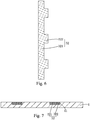
- the through holes each have opposite sidewalls each of which defines an angle that is an obtuse angle with respect to an undersurface of the photoresist zones and also defines an angle that is an acute angle with respect to an upper surface of the photoresist zones.
- the through holes each have a cross section that is an isosceles trapezoid, and isosceles trapezoid has a lower base that is greater than an upper base.
- the backing cavities have a depth of 300-3000nm.
- the backing cavities have a cross section that is rectangular.
- the metal patterns have a thickness that corresponds to the depth of the backing cavities.
- Step S6 comprises:
- the present invention also provides a flexible display panel, which comprises:
- the backing cavities have a depth of 300-3000nm and a cross section that is rectangular.
- the metal patterns has a thickness that corresponds to the depth of the backing cavities.
- the present invention further provides a flexible display panel fabrication method, which comprises the following steps:
- the efficacy of the present invention is that the present invention provides a flexible display panel fabrication method, which first subjects a photoresist layer to patterning to form a plurality of mutually spaced photoresist zones, wherein a through hole is formed between every two adjacent ones of the photoresist zones; and then, subjecting the flexible backing plate to cavity formation with the photoresist zones as a mask so as to form a plurality of mutually parallel backing cavities respectively at locations corresponding to the through holes; and then, depositing a metal film and subsequently removing the photoresist zones and portions of the metal layer located thereon to form a plurality of metal patterns that are embedded in the plurality of mutually parallel backing cavities, wherein each of the metal patterns comprises a scan line and a plurality of gate electrodes; and then, forming a plurality of TFTs that are arranged in an array and OLED light emissive elements.
- the method allows the scan lines and the gate electrodes to be embedded in the flexible backing plate so as to effectively reduce stress defects induced in the scan lines during curving of the flexible display panel and improve the stability of the flexible display panel.
- the present invention provides a flexible display panel, which comprises metal patterns that include scan lines and gate electrodes and are embedded in the baking cavities of a flexible backing plate so as to reduce stress defects induced in the scan lines during curving of the flexible display panel to thereby help improve stability of the flexible display panel.
- the present invention provides a flexible display panel fabrication method, which comprises the following steps:
- Step S6 comprises:
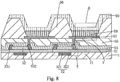
- the method described above allows the metal patterns 32 that include the scan lines 321 and the gate electrodes 322 to be embedded in the backing cavities 11 formed in the flexible backing plate 1 and this is equivalent to forming a combined film of the metal patterns 32 and the flexible backing plate 2.
- the scan lines 321 and the gate electrodes 322 are integrally combined with the flexible backing plate 1 as a unitary structure and this helps spread a stress induced in the scan lines 321 during curving of the display panel thereby effectively reducing stress defects induced in the scan lines 321 during curving of the flexible display panel and thus improving stability of the flexible display panel.
- the present invention also provides a flexible display panel that is fabricated with the above method.
- a flexible display panel which comprises:
- the gate electrode 322, the semiconductor active layer 52, the source electrode 531, and the drain electrode 532 form the TFT T ; and the anode 57, the organic emissive layer 58, and the cathode 59 form the OLED light emissive element D.
- the backing cavities 11 has a depth of 300-3000nm and a cross section that is rectangular, and the metal patterns 32 has a thickness that corresponds to the depth of the backing cavities 11.
- the flexible display panel of the present invention is structured such that the metal patterns 32 that include the scan lines 321 and the gate electrodes 322 is embedded in the backing cavities 11 formed in the flexible backing plate 1 and this is equivalent to forming a combined film of the metal patterns 32 and the flexible backing plate 2.
- the scan lines 321 and the gate electrodes 322 are integrally combined with the flexible backing plate 1 as a unitary structure and this helps spread a stress induced in the scan lines 321 during curving of the display panel thereby effectively reducing stress defects induced in the scan lines 321 during curving of the flexible display panel and thus improving stability of the flexible display panel.
- the present invention provides a flexible display panel fabrication method, which first subjects a photoresist layer to patterning to form a plurality of mutually spaced photoresist zones, wherein a through hole is formed between every two adjacent ones of the photoresist zones; and then, subjecting the flexible backing plate to cavity formation with the photoresist zones as a mask so as to form a plurality of mutually parallel backing cavities respectively at locations corresponding to the through holes; and then, depositing a metal film and subsequently removing the photoresist zones and portions of the metal layer located thereon to form a plurality of metal patterns that are embedded in the plurality of mutually parallel backing cavities, wherein each of the metal patterns comprises a scan line and a plurality of gate electrodes; and then, forming a plurality of TFTs that are arranged in an array and OLED light emissive elements.
- the method allows the scan lines and the gate electrodes to be embedded in the flexible backing plate so as to effectively reduce stress defects induced in the scan lines during curving of the flexible display panel and improve the stability of the flexible display panel.
- the present invention provides a flexible display panel, which comprises metal patterns that include scan lines and gate electrodes and are embedded in the baking cavities of a flexible backing plate so as to reduce stress defects induced in the scan lines during curving of the flexible display panel to thereby help improve stability of the flexible display panel.
Landscapes
- Engineering & Computer Science (AREA)
- Microelectronics & Electronic Packaging (AREA)
- Manufacturing & Machinery (AREA)
- Electroluminescent Light Sources (AREA)
- Devices For Indicating Variable Information By Combining Individual Elements (AREA)
Applications Claiming Priority (2)
| Application Number | Priority Date | Filing Date | Title |
|---|---|---|---|
| CN201710720612.1A CN107342375B (zh) | 2017-08-21 | 2017-08-21 | 柔性显示面板的制作方法及柔性显示面板 |
| PCT/CN2017/101971 WO2019037166A1 (fr) | 2017-08-21 | 2017-09-15 | Procédé de fabrication de panneau d'affichage souple, et panneau d'affichage souple |
Publications (2)
| Publication Number | Publication Date |
|---|---|
| EP3675169A1 true EP3675169A1 (fr) | 2020-07-01 |
| EP3675169A4 EP3675169A4 (fr) | 2021-04-21 |
Family
ID=60215723
Family Applications (1)
| Application Number | Title | Priority Date | Filing Date |
|---|---|---|---|
| EP17922187.4A Withdrawn EP3675169A4 (fr) | 2017-08-21 | 2017-09-15 | Procédé de fabrication de panneau d'affichage souple, et panneau d'affichage souple |
Country Status (6)
| Country | Link |
|---|---|
| US (1) | US10333086B2 (fr) |
| EP (1) | EP3675169A4 (fr) |
| JP (1) | JP2020529047A (fr) |
| KR (1) | KR102315759B1 (fr) |
| CN (1) | CN107342375B (fr) |
| WO (1) | WO2019037166A1 (fr) |
Families Citing this family (18)
| Publication number | Priority date | Publication date | Assignee | Title |
|---|---|---|---|---|
| CN109860207B (zh) * | 2019-02-27 | 2022-07-19 | 合肥鑫晟光电科技有限公司 | 一种阵列基板、其制作方法、显示面板及显示装置 |
| JP6763452B1 (ja) * | 2019-04-15 | 2020-09-30 | 富士ゼロックス株式会社 | 発光装置、光学装置および情報処理装置 |
| US11968866B2 (en) * | 2019-06-20 | 2024-04-23 | Sharp Kabushiki Kaisha | Display device |
| CN110265460A (zh) * | 2019-06-27 | 2019-09-20 | 京东方科技集团股份有限公司 | Oled显示基板及其制作方法、显示装置 |
| CN110752295B (zh) | 2019-11-29 | 2023-04-28 | 武汉天马微电子有限公司 | 柔性显示面板及其制作方法和显示装置 |
| CN111081639B (zh) * | 2019-12-05 | 2022-05-31 | 深圳市华星光电半导体显示技术有限公司 | Cmos薄膜晶体管及其制备方法、显示面板 |
| TW202032226A (zh) * | 2020-01-14 | 2020-09-01 | 友達光電股份有限公司 | 軟性電路結構 |
| CN111180610B (zh) * | 2020-02-20 | 2024-08-16 | 福建华佳彩有限公司 | 一种窄边框的面板结构及制作方法 |
| CN111403467B (zh) * | 2020-03-31 | 2022-09-13 | 武汉天马微电子有限公司 | 显示基板、显示面板和显示装置 |
| CN111613138B (zh) * | 2020-05-19 | 2021-09-03 | 武汉华星光电半导体显示技术有限公司 | 显示面板及显示装置 |
| US11640963B2 (en) | 2020-05-19 | 2023-05-02 | Wuhan China Star Optoelectronics Semiconductor Display Technology Co., Ltd. | Display panel and display device |
| CN111754870B (zh) * | 2020-06-22 | 2022-05-27 | 武汉华星光电半导体显示技术有限公司 | 柔性显示面板及显示装置 |
| CN111785737A (zh) * | 2020-07-15 | 2020-10-16 | Tcl华星光电技术有限公司 | 阵列基板、其制作方法及显示面板 |
| CN112185984B (zh) * | 2020-09-17 | 2022-07-12 | 武汉华星光电半导体显示技术有限公司 | 一种阵列基板及显示面板 |
| CN113053766B (zh) * | 2021-03-08 | 2024-08-02 | 京东方科技集团股份有限公司 | 光刻胶残留检测方法、面板及制造方法和显示装置 |
| CN114784025A (zh) * | 2022-05-26 | 2022-07-22 | Tcl华星光电技术有限公司 | 阵列基板及其制备方法 |
| CN115172164A (zh) * | 2022-07-28 | 2022-10-11 | 北海惠科半导体科技有限公司 | 肖特基二极管及其制备方法 |
| CN115447239A (zh) * | 2022-09-26 | 2022-12-09 | 昆山国显光电有限公司 | 柔性多膜层结构及其制备方法和显示模组 |
Family Cites Families (25)
| Publication number | Priority date | Publication date | Assignee | Title |
|---|---|---|---|---|
| JPS61181164A (ja) * | 1985-02-07 | 1986-08-13 | Matsushita Electric Ind Co Ltd | 薄膜電界効果トランジスタの製造方法 |
| JP2001154218A (ja) * | 1999-09-08 | 2001-06-08 | Matsushita Electric Ind Co Ltd | 表示装置およびその製造方法 |
| US6852997B2 (en) * | 2001-10-30 | 2005-02-08 | Semiconductor Energy Laboratory Co., Ltd. | Light emitting device |
| TW546853B (en) * | 2002-05-01 | 2003-08-11 | Au Optronics Corp | Active type OLED and the fabrication method thereof |
| JP4433404B2 (ja) * | 2005-01-06 | 2010-03-17 | セイコーエプソン株式会社 | 半導体装置、液晶装置、電子デバイス及び半導体装置の製造方法 |
| KR101141533B1 (ko) * | 2005-06-25 | 2012-05-04 | 엘지디스플레이 주식회사 | 기판 반송방법 및 이를 이용한 플렉서블 디스플레이의제조방법 |
| JP2007165860A (ja) * | 2005-11-17 | 2007-06-28 | Semiconductor Energy Lab Co Ltd | 表示装置及びその作製方法 |
| KR101433613B1 (ko) * | 2007-11-01 | 2014-08-27 | 삼성디스플레이 주식회사 | 표시장치의 제조방법 및 이에 의한 표시장치 |
| JP5007246B2 (ja) * | 2008-01-31 | 2012-08-22 | 三菱電機株式会社 | 有機電界発光型表示装置及びその製造方法 |
| KR101274719B1 (ko) * | 2010-06-11 | 2013-06-25 | 엘지디스플레이 주식회사 | 박막트랜지스터 기판 및 그 제조 방법과 그를 가지는 평판 표시 소자 |
| JP6170488B2 (ja) * | 2012-10-18 | 2017-07-26 | 日本化薬株式会社 | 新規縮合多環芳香族化合物及びその用途 |
| CN202916556U (zh) * | 2012-11-16 | 2013-05-01 | 京东方科技集团股份有限公司 | 一种显示基板和具有该显示基板的显示装置 |
| JP2014194517A (ja) * | 2013-02-27 | 2014-10-09 | Sony Corp | 表示装置、表示装置の製造方法、表示装置の駆動方法および電子機器 |
| JP6174877B2 (ja) * | 2013-03-21 | 2017-08-02 | 株式会社半導体エネルギー研究所 | 表示装置及び電子機器 |
| CN103489880B (zh) * | 2013-10-12 | 2015-03-25 | 京东方科技集团股份有限公司 | 一种显示基板和含有该显示基板的柔性显示装置 |
| KR20150075367A (ko) * | 2013-12-25 | 2015-07-03 | 가부시키가이샤 한도오따이 에네루기 켄큐쇼 | 표시 장치 및 전자 기기 |
| JP6596224B2 (ja) * | 2014-05-02 | 2019-10-23 | 株式会社半導体エネルギー研究所 | 発光装置及び入出力装置 |
| KR102296945B1 (ko) * | 2014-07-04 | 2021-09-01 | 엘지디스플레이 주식회사 | 유기 발광 표시 장치 및 그 제조 방법 |
| CN104393002A (zh) * | 2014-10-29 | 2015-03-04 | 合肥京东方光电科技有限公司 | 一种显示基板及其制作方法、显示装置 |
| CN104393019B (zh) * | 2014-11-07 | 2017-11-10 | 京东方科技集团股份有限公司 | 一种显示基板及其制备方法、显示装置 |
| KR102441560B1 (ko) * | 2015-04-07 | 2022-09-08 | 삼성디스플레이 주식회사 | 박막트랜지스터 어레이 기판 및 이를 구비한 유기 발광 표시 장치 |
| KR102399568B1 (ko) * | 2015-09-23 | 2022-05-19 | 삼성디스플레이 주식회사 | 폴딩 가능한 디스플레이 장치 및 그 제조방법 |
| KR102473224B1 (ko) * | 2015-12-31 | 2022-12-01 | 엘지디스플레이 주식회사 | 표시 장치 |
| CN105428245B (zh) * | 2016-01-26 | 2019-03-01 | 京东方科技集团股份有限公司 | 像素结构及其制备方法、阵列基板和显示装置 |
| CN106449660A (zh) * | 2016-11-11 | 2017-02-22 | 京东方科技集团股份有限公司 | 一种阵列基板、其制作方法及显示装置 |
-
2017
- 2017-08-21 CN CN201710720612.1A patent/CN107342375B/zh not_active Expired - Fee Related
- 2017-09-15 EP EP17922187.4A patent/EP3675169A4/fr not_active Withdrawn
- 2017-09-15 KR KR1020207007949A patent/KR102315759B1/ko not_active Expired - Fee Related
- 2017-09-15 JP JP2020506163A patent/JP2020529047A/ja active Pending
- 2017-09-15 US US15/574,831 patent/US10333086B2/en not_active Expired - Fee Related
- 2017-09-15 WO PCT/CN2017/101971 patent/WO2019037166A1/fr not_active Ceased
Also Published As
| Publication number | Publication date |
|---|---|
| KR20200034805A (ko) | 2020-03-31 |
| WO2019037166A1 (fr) | 2019-02-28 |
| CN107342375A (zh) | 2017-11-10 |
| KR102315759B1 (ko) | 2021-10-21 |
| US20190058140A1 (en) | 2019-02-21 |
| EP3675169A4 (fr) | 2021-04-21 |
| JP2020529047A (ja) | 2020-10-01 |
| CN107342375B (zh) | 2019-05-31 |
| US10333086B2 (en) | 2019-06-25 |
Similar Documents
| Publication | Publication Date | Title |
|---|---|---|
| US10333086B2 (en) | Flexible display panel fabrication method and flexible display panel | |
| US11800783B2 (en) | Array substrate, stretchable display device, and method for manufacturing array substrate | |
| US10868263B2 (en) | Flexible display panel and method for manufacturing same | |
| CN107565041B (zh) | 有机发光显示装置及其制造方法 | |
| US10756292B2 (en) | Method of manufacturing an OLED panel and an OLED panel | |
| KR101257734B1 (ko) | 유기전계발광 표시장치 | |
| US9881979B2 (en) | Flexible display device and method for manufacturing the same | |
| JP6253541B2 (ja) | 表示装置 | |
| CN101740607B (zh) | 有机发光显示器件及其制造方法 | |
| CN100514669C (zh) | 有机电致发光显示器件及其制造方法 | |
| CN111725255B (zh) | 显示装置 | |
| US20190156708A1 (en) | Flexible display screen structure and manufacturing method thereof | |
| US20200396837A1 (en) | Flexible base substrate, manufacturing method thereof, display device | |
| JP6872343B2 (ja) | 表示装置および表示装置の製造方法 | |
| KR20150072432A (ko) | 가요성 디스플레이 | |
| JP2004014514A (ja) | Amelディスプレイパネルおよびその製造方法 | |
| CN107359177B (zh) | 一种柔性背板的制作方法、液晶显示面板以及oled显示面板 | |
| JP2017146463A (ja) | 表示装置 | |
| WO2021082178A1 (fr) | Écran d'affichage à diodes électroluminescentes organiques étirable | |
| CN114628481A (zh) | 显示面板及显示装置 | |
| CN108336120A (zh) | 一种阵列基板、显示面板及显示装置 | |
| CN100463213C (zh) | 有机电致发光器件及其制造方法 | |
| CN110112142A (zh) | 阵列基板及其制造方法、显示面板及电子装置 | |
| KR20150087617A (ko) | 표시 기판용 박막 트랜지스터, 표시 기판 및 표시 기판의 제조 방법 | |
| KR20130045299A (ko) | 유기전계발광 표시장치 |
Legal Events
| Date | Code | Title | Description |
|---|---|---|---|
| STAA | Information on the status of an ep patent application or granted ep patent |
Free format text: STATUS: THE INTERNATIONAL PUBLICATION HAS BEEN MADE |
|
| PUAI | Public reference made under article 153(3) epc to a published international application that has entered the european phase |
Free format text: ORIGINAL CODE: 0009012 |
|
| STAA | Information on the status of an ep patent application or granted ep patent |
Free format text: STATUS: REQUEST FOR EXAMINATION WAS MADE |
|
| 17P | Request for examination filed |
Effective date: 20200303 |
|
| AK | Designated contracting states |
Kind code of ref document: A1 Designated state(s): AL AT BE BG CH CY CZ DE DK EE ES FI FR GB GR HR HU IE IS IT LI LT LU LV MC MK MT NL NO PL PT RO RS SE SI SK SM TR |
|
| AX | Request for extension of the european patent |
Extension state: BA ME |
|
| DAV | Request for validation of the european patent (deleted) | ||
| DAX | Request for extension of the european patent (deleted) | ||
| A4 | Supplementary search report drawn up and despatched |
Effective date: 20210324 |
|
| RIC1 | Information provided on ipc code assigned before grant |
Ipc: H01L 29/786 20060101ALI20210318BHEP Ipc: H01L 27/12 20060101AFI20210318BHEP |
|
| STAA | Information on the status of an ep patent application or granted ep patent |
Free format text: STATUS: THE APPLICATION IS DEEMED TO BE WITHDRAWN |
|
| 18D | Application deemed to be withdrawn |
Effective date: 20240403 |