EP3675192B1 - Flexibles substrat und herstellungsverfahren dafür, verfahren zum erfassen einer biegung und flexible anzeigevorrichtung - Google Patents
Flexibles substrat und herstellungsverfahren dafür, verfahren zum erfassen einer biegung und flexible anzeigevorrichtung Download PDFInfo
- Publication number
- EP3675192B1 EP3675192B1 EP18800466.7A EP18800466A EP3675192B1 EP 3675192 B1 EP3675192 B1 EP 3675192B1 EP 18800466 A EP18800466 A EP 18800466A EP 3675192 B1 EP3675192 B1 EP 3675192B1
- Authority
- EP
- European Patent Office
- Prior art keywords
- acoustic wave
- surface acoustic
- passivation layer
- flexible substrate
- layer
- Prior art date
- Legal status (The legal status is an assumption and is not a legal conclusion. Google has not performed a legal analysis and makes no representation as to the accuracy of the status listed.)
- Active
Links
Images



Classifications
-
- G—PHYSICS
- G01—MEASURING; TESTING
- G01B—MEASURING LENGTH, THICKNESS OR SIMILAR LINEAR DIMENSIONS; MEASURING ANGLES; MEASURING AREAS; MEASURING IRREGULARITIES OF SURFACES OR CONTOURS
- G01B17/00—Measuring arrangements characterised by the use of infrasonic, sonic or ultrasonic vibrations
- G01B17/04—Measuring arrangements characterised by the use of infrasonic, sonic or ultrasonic vibrations for measuring the deformation in a solid, e.g. by vibrating string
-
- G—PHYSICS
- G01—MEASURING; TESTING
- G01B—MEASURING LENGTH, THICKNESS OR SIMILAR LINEAR DIMENSIONS; MEASURING ANGLES; MEASURING AREAS; MEASURING IRREGULARITIES OF SURFACES OR CONTOURS
- G01B17/00—Measuring arrangements characterised by the use of infrasonic, sonic or ultrasonic vibrations
- G01B17/06—Measuring arrangements characterised by the use of infrasonic, sonic or ultrasonic vibrations for measuring contours or curvatures
-
- G—PHYSICS
- G01—MEASURING; TESTING
- G01B—MEASURING LENGTH, THICKNESS OR SIMILAR LINEAR DIMENSIONS; MEASURING ANGLES; MEASURING AREAS; MEASURING IRREGULARITIES OF SURFACES OR CONTOURS
- G01B7/00—Measuring arrangements characterised by the use of electric or magnetic techniques
- G01B7/16—Measuring arrangements characterised by the use of electric or magnetic techniques for measuring the deformation in a solid, e.g. by resistance strain gauge
-
- H—ELECTRICITY
- H10—SEMICONDUCTOR DEVICES; ELECTRIC SOLID-STATE DEVICES NOT OTHERWISE PROVIDED FOR
- H10D—INORGANIC ELECTRIC SEMICONDUCTOR DEVICES
- H10D86/00—Integrated devices formed in or on insulating or conducting substrates, e.g. formed in silicon-on-insulator [SOI] substrates or on stainless steel or glass substrates
- H10D86/01—Manufacture or treatment
- H10D86/021—Manufacture or treatment of multiple TFTs
-
- H—ELECTRICITY
- H10—SEMICONDUCTOR DEVICES; ELECTRIC SOLID-STATE DEVICES NOT OTHERWISE PROVIDED FOR
- H10K—ORGANIC ELECTRIC SOLID-STATE DEVICES
- H10K59/00—Integrated devices, or assemblies of multiple devices, comprising at least one organic light-emitting element covered by group H10K50/00
-
- H—ELECTRICITY
- H10—SEMICONDUCTOR DEVICES; ELECTRIC SOLID-STATE DEVICES NOT OTHERWISE PROVIDED FOR
- H10K—ORGANIC ELECTRIC SOLID-STATE DEVICES
- H10K71/00—Manufacture or treatment specially adapted for the organic devices covered by this subclass
-
- H—ELECTRICITY
- H10—SEMICONDUCTOR DEVICES; ELECTRIC SOLID-STATE DEVICES NOT OTHERWISE PROVIDED FOR
- H10K—ORGANIC ELECTRIC SOLID-STATE DEVICES
- H10K71/00—Manufacture or treatment specially adapted for the organic devices covered by this subclass
- H10K71/60—Forming conductive regions or layers, e.g. electrodes
-
- H—ELECTRICITY
- H10—SEMICONDUCTOR DEVICES; ELECTRIC SOLID-STATE DEVICES NOT OTHERWISE PROVIDED FOR
- H10N—ELECTRIC SOLID-STATE DEVICES NOT OTHERWISE PROVIDED FOR
- H10N39/00—Integrated devices, or assemblies of multiple devices, comprising at least one piezoelectric, electrostrictive or magnetostrictive element covered by groups H10N30/00 – H10N35/00
-
- H—ELECTRICITY
- H10—SEMICONDUCTOR DEVICES; ELECTRIC SOLID-STATE DEVICES NOT OTHERWISE PROVIDED FOR
- H10K—ORGANIC ELECTRIC SOLID-STATE DEVICES
- H10K2102/00—Constructional details relating to the organic devices covered by this subclass
- H10K2102/301—Details of OLEDs
- H10K2102/311—Flexible OLED
-
- H—ELECTRICITY
- H10—SEMICONDUCTOR DEVICES; ELECTRIC SOLID-STATE DEVICES NOT OTHERWISE PROVIDED FOR
- H10K—ORGANIC ELECTRIC SOLID-STATE DEVICES
- H10K59/00—Integrated devices, or assemblies of multiple devices, comprising at least one organic light-emitting element covered by group H10K50/00
- H10K59/10—OLED displays
- H10K59/12—Active-matrix OLED [AMOLED] displays
-
- H—ELECTRICITY
- H10—SEMICONDUCTOR DEVICES; ELECTRIC SOLID-STATE DEVICES NOT OTHERWISE PROVIDED FOR
- H10K—ORGANIC ELECTRIC SOLID-STATE DEVICES
- H10K77/00—Constructional details of devices covered by this subclass and not covered by groups H10K10/80, H10K30/80, H10K50/80 or H10K59/80
- H10K77/10—Substrates, e.g. flexible substrates
- H10K77/111—Flexible substrates
-
- Y—GENERAL TAGGING OF NEW TECHNOLOGICAL DEVELOPMENTS; GENERAL TAGGING OF CROSS-SECTIONAL TECHNOLOGIES SPANNING OVER SEVERAL SECTIONS OF THE IPC; TECHNICAL SUBJECTS COVERED BY FORMER USPC CROSS-REFERENCE ART COLLECTIONS [XRACs] AND DIGESTS
- Y02—TECHNOLOGIES OR APPLICATIONS FOR MITIGATION OR ADAPTATION AGAINST CLIMATE CHANGE
- Y02E—REDUCTION OF GREENHOUSE GAS [GHG] EMISSIONS, RELATED TO ENERGY GENERATION, TRANSMISSION OR DISTRIBUTION
- Y02E10/00—Energy generation through renewable energy sources
- Y02E10/50—Photovoltaic [PV] energy
- Y02E10/549—Organic PV cells
Definitions
- Embodiments of the present disclosure relate to a flexible substrate and a fabrication method thereof, a method for detecting bend, and a flexible display device.
- flexible display technologies have been developed rapidly in recent years which has led to great progress in flexible display from screen size to display quality of flexible display. Also referred to as rollable display, the flexible display has many advantages compared with conventional hard-screen display such as impact resistance, strong in shock resistance, light in weight, small in size, convenient to carry, and low in cost.
- document US 4107626A describes a sensors for converting mechanical strain to an electronic digital signal utilizing surface acoustic wave oscillators
- document US 3978731A describes a transducer which uses surface acoustic waves as a means of detecting pressure, acceleration, temperature, stress or strain in a digital manner
- document US 2006/289901A1 describes a monolithic electronic device including a first nitride epitaxial structure including a plurality of nitride epitaxial layers
- document US 2015/207102A1 describes a foldable, flexible display apparatus including a flexible display panel which display an image and includes a display side on which the image is displayed and of which portions thereof face each other in a folded state of the flexible display apparatus.
- Embodiments of the present disclosure disclose a flexible substrate and a fabrication method thereof, a method for detecting a bend, and a flexible display device.
- a flexible substrate comprising, inter alia, a flexible base, and a surface acoustic wave generating element and a surface acoustic wave detecting element positioned on the flexible base.
- the surface acoustic wave generating element and the surface acoustic wave detecting element are configured to detect a bend of the flexible substrate.
- the surface acoustic wave generating element is configured to generate a surface acoustic wave based on an inputted electric signal.
- the surface acoustic wave detecting element is configured to receive the surface acoustic wave to generate an output electric signal.
- the bend of the flexible base causes a change of at least one characteristic of the surface acoustic wave, and causes a change of the output electric signal, so as to detect the bend based on the change of output electric signal.
- the at least one characteristic includes at least one of a frequency, a phase, and an amplitude.
- the surface acoustic wave generating element and the surface acoustic wave detecting element include a piezoelectric layer, and an interdigital electrode positioned on the piezoelectric layer.
- a material of the piezoelectric layer includes any one of ZnO, AlN, and c-BN.
- the flexible substrate further includes a reflective element positioned on at least one of following locations: a side of the surface acoustic wave generating element away from the surface acoustic wave detecting element; and a side of the surface acoustic wave detecting element away from the surface acoustic wave generating element.
- the reflective element is positioned on the piezoelectric layer.
- the flexible substrate further includes a sound absorbing material positioned on at least one of following locations: a side of the surface acoustic wave generating element away from the surface acoustic wave detecting element; and a side of the surface acoustic wave detecting element away from the surface acoustic wave generating element.
- the sound absorbing material is positioned on the piezoelectric layer.
- the flexible base is provided with a plurality of thin film transistors arranged in an array.
- the surface acoustic wave generating element and the surface acoustic wave detecting element are positioned between adjacent thin film transistors.
- a source/drain electrode of the thin-film transistor and the interdigital electrode are formed by the same material.
- the flexible substrate further includes a passivation layer having a first portion positioned in a region where the thin film transistors are positioned and a second portion positioned in a region between the adjacent thin film transistors.
- the surface acoustic wave generating element and the surface acoustic wave detecting element are positioned on the second portion.
- the passivation layer includes a first passivation layer and a second passivation layer positioned on the first passivation layer.
- the flexible substrate further includes a lead positioned on the second portion of the first passivation layer.
- the surface acoustic wave generating element and the surface acoustic wave detecting element are electrically connected to the lead through a via in the second passivation layer.
- the flexible substrate further includes a planarization layer covered on the surface acoustic wave generating element and the surface acoustic wave detecting element.
- the flexible OLED display device includes the flexible substrate according to the present disclosure, such as the flexible substrate according to one or more embodiments disclosed above and/or below in more detail.
- the flexible OLED display device further includes a driver connected to the surface acoustic wave generating element and configured to drive the surface acoustic wave generating element to generate the surface acoustic wave, and a processing unit connected to the surface acoustic wave detecting element and configured to process the output electric signal of the surface acoustic wave detecting element.
- a method for fabricating a flexible substrate according to claim 10 comprising, inter alia: providing a flexible base; and forming a surface acoustic wave generating element and a surface acoustic wave detecting element on the flexible base.
- the surface acoustic wave generating element and the surface acoustic wave detecting element are configured to detect a bend of the flexible substrate.
- forming the surface acoustic wave generating element and the surface acoustic wave detecting element includes: forming a piezoelectric layer on the flexible base; and forming an interdigital electrode on the piezoelectric layer.
- providing the flexible base includes: forming a plurality of thin film transistors arranged in an array on the flexible base; and forming a passivation layer on the flexible base and the plurality of thin film transistors.
- the passivation layer has a first portion positioned in a region where the thin film transistors are positioned and a second portion positioned in a region between the adjacent thin film transistors of the flexible base.
- Forming the piezoelectric layer on the flexible base includes: forming the piezoelectric layer on the second portion of the passivation layer.
- the passivation layer includes a first passivation layer and a second passivation layer positioned on the first passivation layer.
- Providing the flexible base further includes: forming a lead on the second portion of the first passivation layer.
- Forming the surface acoustic wave generating element and the surface acoustic wave detecting element further includes: forming a first via penetrating through the piezoelectric layer and the second portion of the second passivation layer and reaching the lead, before forming the interdigital electrode.
- Forming the interdigital electrode includes: forming a first conducting layer on the piezoelectric layer and in the first via, and patterning the first conducting layer to form the interdigital electrode.
- the method further includes: forming a second via penetrating through the first portion of the passivation layer and reaching a source/drain region of the thin film transistor while forming the first via.
- the first conducting layer further fills the second via, and the patterning the first conducting layer further forms a source/drain electrode of the thin film transistor.
- a method for detecting a bend of the flexible substrate includes: inputting an electric signal to the surface acoustic wave generating element to generate a surface acoustic wave, wherein the bend of the flexible base causes a change of at least one characteristic of the surface acoustic wave; receiving the surface acoustic wave by the surface acoustic wave detecting element to generate an output electric signal, wherein the output electric signal changes based on the change of the at least one characteristic of the surface acoustic wave; and detecting the bend based on the change of the output electric signal.
- Figures 4 and 7 show embodiments of the present invention.
- 1-3,5-6,8-10 show further examples which are not encompassed in the scope of the invention, even if they are named “embodiments” in the corresponding parts of the description.
- the scope of protection is defined by the claims.
- the terms “upper”, “lower”, “right”, “left”, “vertical”, “horizontal”, “top”, “bottom”, and derivatives thereof shall relate to the disclosure, as it is oriented in the drawing figures.
- the terms “overlying”, “atop”, “positioned on “ or “positioned atop” means that a first element, such as a first structure, is present on a second element, such as a second structure, wherein intervening elements, such as an interface structure, e.g. interface layer, may be present between the first element and the second element.
- the term “direct contact” means that a first element, such as a first structure, and a second element, such as a second structure, are connected without any intermediary conducting, insulating or semiconductor layers at the interface of the two elements.
- the expressions “have”, “comprise” and “contain” as well as grammatical variations thereof are used in a non-exclusive way.
- the expression “A has B” as well as the expression “A comprises B” or “A contains B” may both refer to the fact that, besides B, A contains one or more further components and/or constituents, and to the case in which, besides B, no other components, constituents or elements are present in A.
- the bendable characteristic of the flexible display also may provide a convenient human-computer interaction mode.
- Such interaction mode may be implemented by way of bend feedback.
- the screen may be bent to a certain degree, and E-book page flipping may be controlled by detecting the degree of bend.
- Such bend detection function not only may provide an additional interaction mode, but also may implement function control by bending the screen with a glove worn.
- a flexible substrate a bend of which may be detected to provide an additional human-computer interaction.
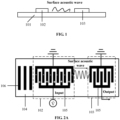
- FIG. 1 schematically illustrates an exemplary sectional view of the flexible substrate according to an embodiment of the present disclosure.
- the flexible substrate may include a flexible base 101, and a surface acoustic wave generating element 102 and a surface acoustic wave detecting element 103 positioned on the flexible base 101.
- the surface acoustic wave generating element 102 and the surface acoustic wave detecting element 103 are configured to detect a bend of the flexible substrate.
- the bend of the flexible substrate may cause a change of a characteristic of the surface acoustic wave. Therefore, the bend of the flexible substrate may be detected based on the change of the surface acoustic wave caused by the bend of the flexible substrate.
- the bend detection function of the flexible substrate may provide the additional human-computer interaction mode. As an example, E-book page flipping may be carried out when the bend is detected. As another example, by means of the bend detection function provided by the flexible substrate, a degree of bend of the substrate may be detected to prevent the substrate from being damaged due to overbending.
- the surface acoustic wave generating element 102 may be configured to generate a surface acoustic wave based on an inputted electric signal.
- the surface acoustic wave detecting element 103 may be configured to receive the surface acoustic wave to generate an output electric signal.
- the bend of the flexible base may cause a change of at least one characteristic of the surface acoustic wave, and then may cause a change of the output electric signal, so as to detect the bend based on the change of output electric signal.
- the at least one characteristic of the surface acoustic wave may be one or more of a phase, a frequency, and an amplitude.
- the flexible base 101 may be formed by a polymer material such as PET, PEN and polyimide.
- FIG. 2A schematically illustrates an exemplary structural diagram of the flexible substrate according to an embodiment of the present disclosure.
- the surface acoustic wave generating element 102 may be an input interdigital transducer
- the surface acoustic wave detecting element 103 may be an output interdigital transducer.
- each of the surface acoustic wave generating element 102 (for example, the input interdigital transducer) and the surface acoustic wave detecting element 103 may include a piezoelectric layer 104 and an interdigital electrode 105 positioned on the piezoelectric layer 104.
- the surface acoustic wave generating element 102 is not limited to the input interdigital transducer as shown in FIG. 2 , and any element capable of generating a surface acoustic wave may serve as the surface acoustic wave generating element 102.
- the surface acoustic wave detecting element 103 is either not limited to the output interdigital transducer as shown in FIG. 2 , and any element capable of converting a surface acoustic wave into an electric signal may serve as the surface acoustic wave detecting element 103.
- an input electric signal may be applied to the input interdigital transducer, and the input interdigital transducer may convert the input electric signal into a surface acoustic wave signal based on an inverse piezoelectric effect.
- the surface acoustic wave signal propagates to the output interdigital transducer along the surface of the piezoelectric layer and is received by the output interdigital transducer.
- the output interdigital transducer converts the surface acoustic wave signal into an electric signal, and outputs the electric signal to for example a processing unit.
- FIG. 3 illustrates a schematic diagram of a change of the surface acoustic wave when the piezoelectric layer is bent according to an embodiment of the present disclosure.
- a characteristic for example, a frequency, a phase or an amplitude
- the bend of the flexible substrate bearing the piezoelectric layer may be obtained by analyzing the change of the output electric signal.
- the flexible substrate provided by embodiments of the present disclosure may detect the bend of the flexible substrate to provide an additional human-computer interaction mode based on a degree and/or direction of the bend. Moreover, the degree of the bend may be detected based on the bend to prevent the flexible substrate from being damaged due to overbending.
- the interdigital electrode 105 may be made from metal or metal alloy, such as aluminum or aluminum alloy.
- the aluminum alloy may be aluminum-copper alloy (wherein copper accounts for 25% of the total amount of the aluminum-copper alloy) or aluminum-titanium alloy (wherein titanium accounts for 25% of the total amount of the aluminum-titanium alloy).
- a material of the piezoelectric layer 104 may include any one of ZnO, AlN, and c-BN. Parameters of several materials used for the piezoelectric layer are listed in Table I, for example, sound velocity, mass density, lattice constant, elastic modulus, and thermal conductivity. Table I: Materials of the Piezoelectric Layer Piezoelectric materials Sound velocity Mass density Lattice constant Elastic modulus Thermal conductivity (m/s) (g/cm 3 ) (nm) (Gpa) (W/cm/K) ZnO 2600-3000 5.68 0.32498 211 0.54 AlN 5500-6100 3.26 0.3082 308 2.6 c-BN 8000-10000 3.48 0.3615 830 13
- the flexible substrate may further include a reflective element 106, which may be positioned on a side of the surface acoustic wave generating element 102 away from the surface acoustic wave detecting element 103.
- a reflective element 106 By arranging the reflective element 106, the surface acoustic wave generated by the input interdigital transducer may be reflected to the output interdigital transducer to reduce loss of the surface acoustic wave.
- the reflective element 106 may be positioned on a side of the input interdigital transducer away from the output interdigital transducer. That is, the input interdigital transducer is positioned between the reflective element and the output interdigital transducer.
- this portion of the surface acoustic wave generated by the input interdigital transducer may be reflected to the output interdigital transducer, such that the output interdigital transducer may receive this portion of the surface acoustic wave.
- the reflective element 106 also may be arranged on a side of the surface acoustic wave detecting element 103 away from the surface acoustic wave generating element 102. That is, the surface acoustic wave detecting element 103 may be positioned between the surface acoustic wave generating element 102 and the reflective element 106. Alternatively, the reflective element 106 may be arranged both on the side of the surface acoustic wave generating element 102 away from the surface acoustic wave detecting element 103 and on the side of the surface acoustic wave detecting element 103 away from the surface acoustic wave generating element 102.
- the reflective element 106 may be arranged in a form of a reflective grating, as shown in FIG. 2A .
- the reflective element 106 also may be configured to generate a resonance oscillation of the surface acoustic wave generated by the surface acoustic wave generating element 102 to enhance the surface acoustic wave signal.
- the reflective element 106 may be arranged on the piezoelectric layer 104.
- the reflective element 106 may be made from the same material as the interdigital electrode 105.
- the reflective element 106 may be made from a metallic material. With this configuration, the interdigital electrode 105 and the reflective element 106 may be simultaneously formed by using one-step patterning process.
- FIG. 2B schematically illustrates an exemplary structural diagram of another flexible substrate according to an embodiment of the present disclosure.
- a sound absorbing material 210 is employed to replace the reflective element 106 in the embodiment as shown in FIG. 2A , whereas other structures are the same as the flexible substrate in the embodiment as shown in FIG. 2A .
- the sound absorbing material 210 may be arranged on a side of the surface acoustic wave generating element 102 away from the surface acoustic wave detecting element 103.
- the sound absorbing material 210 also may be arranged on a side of the surface acoustic wave detecting element 103 away from the surface acoustic wave generating element 102. Alternatively, the sound absorbing material 210 also may be arranged both on the side of the surface acoustic wave generating element 102 away from the surface acoustic wave detecting element 103 and the side of the surface acoustic wave detecting element 103 away from the surface acoustic wave generating element 102.
- unemployed surface acoustic wave may be absorbed, such that signal interference between adjacent devices may be prevented.
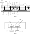
- FIG. 4 schematically illustrates a sectional view of another flexible substrate according to an embodiment of the present disclosure.
- the flexible substrate 200 may be a backplate of a flexible OLED display.
- the flexible substrate likewise includes the flexible base 101, the surface acoustic wave generating element 102, the surface acoustic wave detecting element 103, and the reflective element 106 as in the embodiment shown in FIG. 1 . Therefore, reference may be made to the embodiment as shown in FIG. 1 with respect to the explanation or description of these parts in this embodiment.
- the flexible substrate may further include a plurality of thin film transistors (TFT) 107 arranged in an array on the flexible base 101.
- TFT thin film transistors
- the surface acoustic wave generating element 102 and the surface acoustic wave detecting element 103 are positioned between the adjacent thin film transistors 107.
- Each of the thin film transistors 107 may include a gate on the flexible base 101, a gate insulation layer on the gate and a region between the adjacent thin film transistors 107 of the flexible base 101, and a source/drain region and a channel region on the gate insulation layer.
- the flexible substrate may further include a source/drain electrode 1071 electrically contacting the source/drain region of the thin film transistor.
- the source/drain electrode 1071 and the interdigital electrode 105 may be formed by the same material such as metal. With this configuration, the source/drain electrode and the interdigital electrode may be simultaneously fabricated by using one-step patterning process.
- the flexible substrate may further include a passivation layer 108 having a first portion 108A positioned in a region where the thin film transistors 107 are positioned and a second portion 108B positioned in a region between the adjacent thin film transistors 107 of the flexible base 101.
- the surface acoustic wave generating element 102 and the surface acoustic wave detecting element 103 may be positioned on the second portion 108B of the passivation layer 108.
- the passivation layer 108 may include a first passivation layer 1081 and a second passivation layer 1082 positioned on the first passivation layer 1081.
- both the first passivation layer 1081 and the second passivation layer 1082 may include SiO, SiN, or a lamination layer thereof.
- the flexible substrate may further include a lead 109 positioned on the second portion 108B of the first passivation layer 1081, and the surface acoustic wave generating element 102 and the surface acoustic wave detecting element 103 may electrically contact the lead 109 through a via in the second passivation layer 1082.
- the flexible substrate may further include a planarization layer 110 covered on the surface acoustic wave generating element 102 and the surface acoustic wave detecting element 103 to prevent outside environment from having a negative effect on the ultrasonic wave signal.
- the planarization layer 110 may be covered on the second passivation layer 1082, the source/drain electrode 1071, and the interdigital electrode 105.
- the flexible substrate may further include a conducting layer 111 positioned on the planarization layer 110 and a pixel defining layer 112 formed on the conducting layer 111.
- the planarization layer 110 may include a photoresist, which can prevent negative effects on the surface acoustic wave generating element 102 and the surface acoustic wave detecting element 103.
- the conducting layer 111 electrically contacts the source/drain electrode 1071 through a via in the planarization layer 110, and the conducting layer 111 may serve as an anode electrode of the flexible OLED display device.
- a vertical projection of the pixel defining layer 112 covers the via in the planarization layer 110.
- the pixel defining layer 112 may define a pixel region of the flexible OLED display device, such that an organic light-emitting material may be deposited in the pixel region.
- the flexible OLED display device may include the flexible substrate according to the present disclosure, such as the flexible substrate according to one or more embodiments disclosed above and/or below in more detail. Therefore, reference may be made to embodiments of the flexible substrate for an alternative embodiment of the flexible OLED display device.
- FIG. 5 schematically illustrates an exemplary block diagram of the flexible OLED display device according to an embodiment of the present disclosure.
- the flexible OLED display device may include the flexible substrate 100 according to the present disclosure.
- the flexible OLED display device may further include a driver 501 connected to the surface acoustic wave generating element 102 and configured to drive the surface acoustic wave generating element 102 to generate the surface acoustic wave, and a processing unit 502 connected to the surface acoustic wave detecting element 103 and configured to receive and process the output electric signal from the surface acoustic wave detecting element 103.
- a driver 501 connected to the surface acoustic wave generating element 102 and configured to drive the surface acoustic wave generating element 102 to generate the surface acoustic wave
- a processing unit 502 connected to the surface acoustic wave detecting element 103 and configured to receive and process the output electric signal from the surface acoustic wave detecting element 103.
- an operating frequency of the surface acoustic wave generating element 102 ranges from several tens of MHZ to several GHZ, which is greater than a drive frequency of the thin film transistor. Therefore, in an embodiment of the present disclosure, the driver 501 configured to drive the surface acoustic wave generating element to generate the surface acoustic wave may be separately arranged.
- FIG. 6 schematically illustrates a drive circuit diagram of the flexible OLED display device according to an embodiment of the present disclosure.
- the surface acoustic wave generating element 102 and the surface acoustic wave detecting element 103 may be positioned in a region, where no thin film transistor 107 is arranged, in each pixel region of the display device.
- the driver 501 may be electrically connected to the interdigital electrode of the surface acoustic wave generating element 102, and is configured to drive the surface acoustic wave generating element 102 to generate a surface acoustic wave.
- the processing unit 502 may be electrically connected to the interdigital electrode of the surface acoustic wave detecting element 103, and is configured to receive and process the output electric signal from the surface acoustic wave detecting element 103 to determine the bend of the flexible OLED display device.
- the flexible OLED display device may further include a gate driver 601 electrically connected to a gate (G) of the thin film transistor, and a source driver 602 electrically connected to a source (S) of the thin film transistor 107.
- the gate driver 601 provides a drive signal to the thin film transistor
- the source driver 602 provides a data signal to the thin film transistor.
- the processing unit 502 may be implemented as a combination of a processor and a memory, wherein the processor executes a program stored in the memory to implement a functionality of the processing unit.
- the gate driver 601, the source driver 602 and the driver 501 either may be implemented only by way of a hardware circuit, such as, an analog circuit or a digital circuit, or may be implemented by a combination of a circuit and a software and/or a firmware, such as for example, a digital signal processor, software and a memory working together to trigger various functions to be executed.
- FIG. 7 schematically illustrates a sectional view of another flexible OLED display device according to an embodiment of the present disclosure.
- the flexible OLED display device includes the flexible substrate in the embodiment as shown in FIG. 4 , an organic light emitting layer 113 positioned in the pixel region defined by the pixel defining layer 112, a cathode layer 114 positioned on the organic light emitting layer 113 and the pixel defining layer 112, and a buffer layer 115 positioned on the cathode layer 114.
- the bend of the flexible OLED display device may be detected based on the change of the surface acoustic wave caused by the bend of the flexible OLED display device.
- an additional human-computer interaction mode may be provided for the flexible OLED display device, for example, an E-book page flipping operation when the bend is detected.
- a degree of bend of the flexible OLED display device may be detected to prevent the flexible OLED display device from being damaged due to overbending.
- a method for fabricating a flexible substrate may be used for fabricating the flexible substrate according to the present disclosure, such as the flexible substrate according to one or more embodiments disclosed above and/or below in more detail. Therefore, reference may be made to the embodiments of the flexible substrate for alternative embodiments of the method.
- the method may include the following steps, which may be performed in given order or in a different order. Furthermore, additional method steps not listed may be provided which are not listed. Furthermore, two or more or event all of the method steps may be performed at least partially simultaneously. Furthermore, a method step may be performed twice or even more than twice, repeatedly.
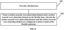
- FIG. 8 schematically illustrates a flowchart of a method for fabricating a flexible substrate according to an embodiment of the present disclosure.
- the method includes Step S81 and Step S82.
- Step S81 a flexible base is provided.
- Step S82 a surface acoustic wave generating element and a surface acoustic wave detecting element are formed on the flexible base.
- the surface acoustic wave generating element and the surface acoustic wave detecting element are configured to detect a bend of the flexible substrate.
- providing the flexible base may include: forming a plurality of thin film transistors arranged in an array on the flexible base; and forming a passivation layer on the flexible base and the plurality of thin film transistors.
- the passivation layer has a first portion positioned on the thin film transistors and a second portion positioned in a region between the adjacent thin film transistors of the flexible base.
- forming the surface acoustic wave generating element and the surface acoustic wave detecting element may include: forming a piezoelectric layer on the flexible base; and forming an interdigital electrode on the piezoelectric layer.
- the piezoelectric layer may be formed on the second portion of the passivation layer, such that the surface acoustic wave generating element and the surface acoustic wave detecting element are formed between the adjacent thin film transistors.
- the passivation layer may include a first passivation layer and a second passivation layer positioned on the first passivation layer.
- Providing the flexible base may further include: forming a lead on the second portion of the first passivation layer.
- forming the surface acoustic wave generating element and the surface acoustic wave detecting element may further include: forming a first via penetrating through the piezoelectric layer and the second portion of the second passivation layer and reaching the lead, before forming the interdigital electrode.
- forming the interdigital electrode may include: forming a first conducting layer on the piezoelectric layer and in the first via, and patterning the first conducting layer to form the interdigital electrode. The interdigital electrode electrically contacts the lead through the conducting layer in the first via.
- the method for fabricating the flexible substrate may further include: forming a second via penetrating through the first portion of the passivation layer and reaching a source/drain region of the thin film transistor while forming the first via.
- the first conducting layer fills the second via. Patterning the first conducting layer further forms a source/drain electrode of the thin film transistor. That is, the interdigital electrode and the source/drain electrode may be formed in one-step patterning process. Therefore, the method for fabricating the flexible substrate provided by this embodiment of the present disclosure is relatively simple in process.
- the method for fabricating the flexible substrate may further include: forming a planarization layer covering the second passivation layer, the source/drain electrode and the interdigital electrode; forming a third via exposing the source/drain electrode in the planarization layer; forming a second conducting layer on the planarization layer and in the third via; and forming a pixel defining layer on the second conducting layer, wherein a vertical projection of the pixel defining layer covers the second via.
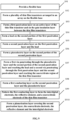
- FIG. 9 schematically illustrates a flowchart of a method for fabricating the flexible substrate in FIG. 4 according to an embodiment of the present disclosure.
- the fabricated flexible substrate may be used as a backplate of the flexible OLED display device.
- the method may include Steps S91-S910.
- a flexible base 101 is provided.
- the flexible base 101 may be formed by a polymer material such as PET, PEN and polyimide.
- each of the thin film transistors 107 may include a gate, a gate insulation layer, an active layer (including a source/drain region and a channel region).
- a first passivation layer 1081 is formed on the active layer of the thin film transistor 107 and on the gate insulation layer between the adjacent thin film transistors.
- the first passivation layer 1081 includes a first portion 108A positioned on the thin film transistor 107 and a second portion 108B between the adjacent thin film transistors 107.
- the material of the first passivation layer 1081 may be, for example, SiO, SiN, or a combination of SiO and SiN.
- a lead 109 is formed on the second portion 108B of the first passivation layer 1081.
- the lead 109 may be formed by way of sputtering, evaporation, and so on.
- a second passivation layer 1082 is formed on the first passivation layer 1081 and the lead 109.
- the second passivation layer 1082 includes a first portion 108A positioned on the thin film transistor 107 and a second portion 108B between the adjacent thin film transistors 108.
- the material of the second passivation layer 1082 may be, for example, SiO, SiN, or a combination of SiO and SiN.
- a piezoelectric layer 104 is formed on the second portion 108B of the second passivation layer 1082.
- the material of the piezoelectric layer 104 may include, for example, any one of ZnO, AlN, and c-BN.
- Step S97 a first via penetrating through the piezoelectric layer 104 and the second portion 108B of the second passivation layer 1082 and reaching the lead 109 and a second via penetrating through the first passivation layer 1081 and the second passivation layer 1082 and reaching the source/drain region of the thin film transistor 107 are formed.
- Step S98 a first conducting layer is formed on the second passivation layer 1082 and the piezoelectric layer 104, and the first conducting layer electrically contacts the lead 109 and the source/drain region through the first via and the second via, respectively.
- Step S99 the first conducting layer is patterned to form the interdigital electrode 105, the reflective element 106, and a source/drain electrode 1071 of the thin film transistor.
- Step S910 a planarization layer 110 covering the second passivation layer 1082, the source/drain electrode 1071, the reflective element 106 and the interdigital electrode 105 is formed.
- the method in the embodiment as shown in FIG. 9 may further include steps of forming other known parts or components required.
- the method for fabricating the flexible substrate may further include: forming a third via exposing the source/drain electrode 1071 in the planarization layer 110; forming a second conducting layer 111 on the planarization layer 110 and in the third via; and forming a pixel defining layer 112 on the second conducting layer 111.
- the pixel defining layer 112 fills the third via, and the vertical projection of the pixel defining layer 112 covers the third via. Detailed description of these steps is omitted in this embodiment.
- a method for detecting a bend of a flexible substrate there is provided a method for detecting a bend of a flexible substrate.
- this method may be used to detect the bend of the flexible substrate according to the present disclosure, such as the flexible substrate according to one or more embodiments disclosed above and/or below in more detail. Therefore, reference may be made to the embodiments of the flexible substrate for alternative embodiments of the method.
- FIG. 10 schematically illustrates a flowchart of a method for detecting a bend of a flexible substrate according to an embodiment of the present disclosure. As shown in FIG. 10 , this method includes Steps S11-S13.
- Step S11 an electric signal is inputted to the surface acoustic wave generating element to generate a surface acoustic wave.
- the bend of the flexible base may cause a change of at least one characteristic of the surface acoustic wave.
- the surface acoustic wave generating element may be, for example, a surface acoustic wave input interdigital transducer.
- the inputted electric signal may allow the input interdigital transducer to generate a surface acoustic wave on a surface of the piezoelectric layer based on an inverse piezoelectric effect, wherein the surface acoustic wave propagates on the surface of the piezoelectric layer.
- the piezoelectric layer is subject to an external influence (for example, a stress generated by the bend of the flexible base), at least one characteristic of the surface acoustic wave may be changed.
- the at least one characteristic may include at least one of a frequency, a phase, and an amplitude.
- Step S12 the surface acoustic wave is received by the surface acoustic wave detecting element to generate an output electric signal.
- the output electric signal changes based on the change of the at least one characteristic of the surface acoustic wave.
- the surface acoustic wave detecting element may be, for example, a surface acoustic wave output interdigital transducer.
- the output interdigital transducer may convert the received surface acoustic wave signal into the output electric signal based on the piezoelectric effect.
- the output electric signal may change with the change of the surface acoustic wave.
- Step S13 the bend of the flexible substrate is detected based on the change of the output electric signal.
- the output electric signal changes with the change of the surface acoustic wave. Therefore, the change of the surface acoustic wave may be obtained by processing and analyzing the output electric signal, and then a bending stress distribution of the flexible substrate may be obtained based on the change of the surface acoustic wave, so as to give a feedback based on the bending stress distribution.
- a bending stress distribution of the flexible substrate may be obtained based on the change of the surface acoustic wave, so as to give a feedback based on the bending stress distribution.
- an additional human-computer interaction mode is provided, for example, E-book page flipping.
Landscapes
- Engineering & Computer Science (AREA)
- Manufacturing & Machinery (AREA)
- Physics & Mathematics (AREA)
- General Physics & Mathematics (AREA)
- Electroluminescent Light Sources (AREA)
- Devices For Indicating Variable Information By Combining Individual Elements (AREA)
- Surface Acoustic Wave Elements And Circuit Networks Thereof (AREA)
- Thin Film Transistor (AREA)
Claims (12)
- Flexibles Substrat miteiner flexiblen Basis (101), die mit einer Anzahl in einem Array angeordneter Dünnfilmtransistoren (107) ausgestattet ist,einem akustische Oberflächenwellen erzeugenden Element (102) und einem auf der flexiblen Basis (101) angeordneten akustische Oberflächenwellen erfassenden Element (103),wobei das akustische Oberflächenwellen erzeugende Element (102) und das akustische Oberflächenwellen erfassende Element (103) dazu ausgelegt sind, eine Biegung des flexiblen Substrats zu erfassen, undeiner Passivierungsschicht (108) auf der flexiblen Basis (101) und der Anzahl Dünnfilmtransistoren (107), wobei die Passivierungsschicht (108) einen ersten Abschnitt (108A), der in einem Gebiet angeordnet ist, in dem die Dünnfilmtransistoren (107) angeordnet sind, und einen zweiten Abschnitt (108B), der in einem zwischen den angrenzenden Dünnfilmtransistoren (107) angeordnet ist, aufweist, wobei das akustische Oberflächenwellen erzeugende Element (102) und das akustische Oberflächenwellen erfassende Element (103) auf dem zweiten Abschnitt (108B) angeordnet sind,wobei das akustische Oberflächenwellen erzeugende Element (102) und das akustische Oberflächenwellen erfassende Element (103)eine piezoelektrische Schicht (104) undeine auf der piezoelektrischen Schicht (104) angeordnete interdigitale Elektrode (105)aufweisen, undwobei die piezoelektrische Schicht (104) auf einer von der flexiblen Basis (101) abgewandten Seite eines Kanalgebiets der Dünnfilmtransistoren (107) angeordnet ist und durch die Passivierungsschicht (108) vom Kanalgebiet der Dünnfilmtransistoren (107) elektrisch isoliert ist.
- Flexibles Substrat gemäß Anspruch 1, wobei das akustische Oberflächenwellen erzeugende Element (102) dazu ausgelegt ist, eine auf einem eingegebenen elektrischen Signal basierende akustische Oberflächenwelle zu erzeugen,wobei das akustische Oberflächenwellen erfassende Element (103) dazu ausgelegt ist, die akustische Oberflächenwelle zu empfangen, um ein elektrisches Ausgangssignal zu erzeugen, undwobei das Biegen der flexiblen Basis (101) eine Änderung mindestens eines Merkmals der akustischen Oberflächenwelle bewirkt und eine Änderung des elektrischen Ausgangssignals bewirkt, wodurch die Biegung entdeckt wird, und wobei das mindestens eine Merkmal mindestens eins von einer Frequenz, einer Phase und einer Amplitude aufweist.
- Flexibles Substrat gemäß Anspruch 1 oder 2, wobei ein Material der piezoelektrischen Schicht (104) irgendeins von ZnO, AlN und c-BN aufweist.
- Flexibles Substrat gemäß Anspruch 3, das außerdem ein reflektierendes Element (106) aufweist, das an mindestens einer der folgenden Stellen angeordnet ist:einer von dem die akustische Oberflächenwelle erfassenden Element (103) abgewandten Seite des die akustische Oberflächenwelle erzeugenden Elements (102), wobei das reflektierende Element (106) wahlweise auf der piezoelektrischen Schicht (104 angeordnet ist, undeiner von dem die akustische Oberflächenwelle erzeugenden Element (102) abgewandten Seite des die akustische Oberflächenwelle erfassenden Elements (103), wobei das reflektierende Element (106) wahlweise auf der piezoelektrischen Schicht (104 angeordnet ist.
- Flexibles Substrat gemäß Anspruch 3, das außerdem ein Schall absorbierendes Material (210) aufweist, das an mindestens einer der folgenden Stellen angeordnet ist:einer von dem die akustische Oberflächenwelle erfassenden Element (103) abgewandten Seite des die akustische Oberflächenwelle erzeugenden Elements (102), wobei das Schall absorbierende Material (210) wahlweise auf der piezoelektrischen Schicht (104 angeordnet ist, undeiner von dem die akustische Oberflächenwelle erzeugenden Element (102) abgewandten Seite des die akustische Oberflächenwelle erfassenden Elements (103), wobei das Schall absorbierende Material (210) wahlweise auf der piezoelektrischen Schicht (104 angeordnet ist.
- Flexibles Substrat gemäß einem der Ansprüche 3 bis 5, wobei eine Source/Drain-Elektrode (1071) des Dünnfilmtransistors und die interdigitale Elektrode (105) aus demselben Material gefertigt sind.
- Flexibles Substrat gemäß Anspruch 1, wobei die Passivierungsschicht (108) eine erste Passivierungsschicht (1081) und eine auf der ersten Passivierungsschicht (1081) angeordnete zweite Passivierungsschicht (1082) aufweist, wobei das flexible Substrat außerdem eine Leitung (109) aufweist, die auf dem zweiten Abschnitt (108B) der ersten Passivierungsschicht (1081) angeordnet ist, und wobei das akustische Oberflächenwellen erzeugende Element (102) und das akustische Oberflächenwellen erfassende Element (103) durch einen Durchgang in der zweiten Passivierungsschicht (1082) mit der Leitung (109) verbunden sind.
- Flexibles Substrat gemäß einem der Ansprüche 1 bis 7, das außerdem eine auf dem akustische Oberflächenwellen erzeugenden Element (102) und dem akustische Oberflächenwellen erfassenden Element (103) bedeckte Planarisierungsschicht (110) aufweist.
- Flexible OLED-Anzeigevorrichtung, die das flexible Substrat (100) gemäß einem der Ansprüche 1 bis 8 aufweist, wobei die flexible OLED-Anzeigevorrichtung außerdemeinen Treiber (501), der mit dem akustische Oberflächenwellen erzeugenden Element (102) verbundenen ist und dazu ausgelegt ist, das akustische Oberflächenwellen erzeugende Element (102) zu treiben, um die akustische Oberflächenwelle zu erzeugen, undeine Verarbeitungseinheit (502), die mit dem akustische Oberflächenwellen erfassenden Element (103) verbunden ist und dazu ausgelegt ist, das elektrische Ausgangssignal des die akustische Oberflächenwelle erfassenden Elements (103) zu verarbeiten,aufweist.
- Verfahren zum Herstellen eines flexiblen Substrats mitBereitstellen (S81) einer flexiblen Basis (101) undBilden (S82) eines akustische Oberflächenwellen erzeugenden Elements (102) und eines akustische Oberflächenwellen erfassenden Elements (103) auf der flexiblen Basis (101), wobei das akustische Oberflächenwellen erzeugende Element (102) und das akustische Oberflächenwellen erfassende Element (103) dazu ausgelegt sind, eine Biegung des flexiblen Substrats zu erfassen,wobei das Bereitstellen (S81) einer flexiblen Basis (101)Bilden einer auf der flexiblen Basis (101) in einem Array angeordneten Anzahl Dünnschichttransistoren (107) undBilden einer Passivierungsschicht (108) auf der flexiblen Basis (101) und der Anzahl Dünnschichttransistoren (107),
aufweist,wobei das Bilden (S82) des akustische Oberflächenwellen erzeugenden Elements (102) und des akustische Oberflächenwellen erfassenden Elements (103) auf der flexiblen Basis (101)Bilden einer piezoelektrischen Schicht (104) auf der flexiblen Basis (101) undBilden einer interdigitalen Elektrode (105) auf der piezoelektrischen Schicht (104)
aufweist,und wobei die piezoelektrische Schicht (104) auf einer von der flexiblen Basis (101) abgewandten Seite eines Kanalgebiets der Dünnfilmtransistoren (107) angeordnet ist und durch die Passivierungsschicht (108) vom Kanalgebiet der Dünnfilmtransistoren (107) elektrisch isoliert ist,wobei die Passivierungsschicht (108) einen ersten Abschnitt (108A), der in einem Gebiet angeordnet ist, in dem die Dünnfilmtransistoren (107) angeordnet sind, und einen zweiten Abschnitt (108B), der in einem zwischen den angrenzenden Dünnfilmtransistoren (107) angeordnet ist, aufweist, und wobeiBilden der piezoelektrischen Schicht (104) auf der flexiblen Basis (101)Bilden der piezoelektrischen Schicht 104) auf dem zweiten Abschnitt (108B) der Passivierungsschicht (108)aufweist. - Verfahren gemäß Anspruch 10, wobei die Passivierungsschicht (108) eine erste Passivierungsschicht (1081) und eine auf der ersten Passivierungsschicht (1081) angeordnete zweite Passivierungsschicht (1082) aufweist,wobei das Bereitstellen der flexiblen Basis (101) außerdemBilden einer Leitung (109) auf dem zweiten Abschnitt (108B) der ersten Passivierungsschicht (1081)
aufweist,wobei das Bilden des akustische Oberflächenwellen erzeugenden Elements (102) und des akustische Oberflächenwellen erfassenden Elements (103) außerdem:Bilden eines ersten Durchgangs durch die piezoelektrische Schicht (104) und den zweiten Abschnitt (108B) der zweiten Passivierungsschicht (1082) und Erreichen der Leitung (109) vor dem Bilden der interdigitalen Elektrode (105)
aufweist, undwobei das Bilden der interdigitalen Elektrode (105)Bilden einer ersten leitenden Schicht (111) auf der piezoelektrischen Schicht (104) und im ersten Durchgang undStrukturieren der ersten leitenden Schicht (111) zum Bilden der interdigitalen Elektrode (105)
aufweist,wobei das Verfahren wahlweise außerdemBilden eines zweiten Durchgangs durch den ersten Abschnitt (108A) der Passivierungsschicht (108) und Erreichen eines Source/Drain-Gebiets des Dünnfilmtransistors (107) während des Bildens des ersten Durchgangs aufweist,wobei die erste leitende Schicht (111) außerdem den zweiten Durchgang ausfüllt,und das Strukturieren der ersten leitenden Schicht (111) außerdem eine Source/Drain-Elektrode (1071) des Dünnfilmtransistors (107) bildet. - Verfahren zum Erkennen einer Biegung im flexiblen Substrat gemäß einem der Ansprüche 1 bis 8 mitEingeben (S 11) eines elektrischen Signals in das akustische Oberflächenwellen erzeugende Element (102), um eine akustische Oberflächenwelle zu erzeugen, wobei das Biegen der flexiblen Basis (101) eine Veränderung mindestens eines Merkmals der akustischen Oberflächenwelle bewirkt,Empfangen (S12) der akustischen Oberflächenwelle durch das akustische Oberflächenwellen erfassende Element (103), um ein elektrisches Ausgangssignal zu erzeugen, wobei sich das elektrische Ausgangssignal auf der Grundlage der Änderung des mindestens einen Merkmals der akustischen Oberflächenwelle ändert, undErfassen (S13) der Biegung auf der Grundlage der Änderung des elektrischen Ausgangssignals.
Applications Claiming Priority (2)
| Application Number | Priority Date | Filing Date | Title |
|---|---|---|---|
| CN201710740020.6A CN109427975B (zh) | 2017-08-23 | 2017-08-23 | 柔性基板及其制备方法、检测弯曲的方法以及柔性显示装置 |
| PCT/CN2018/087262 WO2019037485A1 (zh) | 2017-08-23 | 2018-05-17 | 柔性基板及其制备方法、检测弯曲的方法以及柔性显示装置 |
Publications (3)
| Publication Number | Publication Date |
|---|---|
| EP3675192A1 EP3675192A1 (de) | 2020-07-01 |
| EP3675192A4 EP3675192A4 (de) | 2021-05-12 |
| EP3675192B1 true EP3675192B1 (de) | 2024-07-24 |
Family
ID=65438389
Family Applications (1)
| Application Number | Title | Priority Date | Filing Date |
|---|---|---|---|
| EP18800466.7A Active EP3675192B1 (de) | 2017-08-23 | 2018-05-17 | Flexibles substrat und herstellungsverfahren dafür, verfahren zum erfassen einer biegung und flexible anzeigevorrichtung |
Country Status (5)
| Country | Link |
|---|---|
| US (1) | US20220099437A9 (de) |
| EP (1) | EP3675192B1 (de) |
| JP (1) | JP7238247B2 (de) |
| CN (1) | CN109427975B (de) |
| WO (1) | WO2019037485A1 (de) |
Families Citing this family (8)
| Publication number | Priority date | Publication date | Assignee | Title |
|---|---|---|---|---|
| JPWO2019159614A1 (ja) * | 2018-02-13 | 2021-01-28 | パナソニックIpマネジメント株式会社 | 無線通信半導体装置およびその製造方法 |
| CN110309898B (zh) * | 2019-06-21 | 2023-05-23 | 青岛罗博智慧教育技术有限公司 | 纸张页码检测方法、系统和手写板装置 |
| CN110571258B (zh) * | 2019-09-18 | 2022-01-11 | 京东方科技集团股份有限公司 | 显示装置、显示面板、阵列基板及其制造方法 |
| EP4130654A4 (de) * | 2020-08-06 | 2024-03-20 | Murata Manufacturing Co., Ltd. | Vorrichtung zur erkennung der verformung |
| CN112037700B (zh) * | 2020-08-20 | 2022-12-06 | 武汉华星光电半导体显示技术有限公司 | 显示面板的应力测试装置及应力测试方法 |
| CN114964458B (zh) * | 2021-02-25 | 2025-05-16 | 京东方科技集团股份有限公司 | 振动器及制作方法、触觉再现器件及振动波形检测方法 |
| CN115183708A (zh) * | 2021-04-06 | 2022-10-14 | 纬湃汽车电子(长春)有限公司 | 形变检测方法、形变检测系统及电池 |
| CN115332290B (zh) * | 2022-07-18 | 2024-05-28 | 之江实验室 | 一种集成声流控saw器件与薄膜晶体管器件的传感器及其制备方法、应用 |
Family Cites Families (24)
| Publication number | Priority date | Publication date | Assignee | Title |
|---|---|---|---|---|
| US3978731A (en) * | 1974-02-25 | 1976-09-07 | United Technologies Corporation | Surface acoustic wave transducer |
| US4107626A (en) * | 1976-12-20 | 1978-08-15 | Gould Inc. | Digital output force sensor using surface acoustic waves |
| JPS63307326A (ja) * | 1987-06-09 | 1988-12-15 | Fujikura Ltd | 圧力センサとその製造方法 |
| JP3868567B2 (ja) * | 1997-01-18 | 2007-01-17 | 株式会社半導体エネルギー研究所 | 複合化回路の作製方法 |
| US6340957B1 (en) * | 1997-08-29 | 2002-01-22 | Xerox Corporation | Dynamically relocatable tileable displays |
| JP3780947B2 (ja) | 2002-01-18 | 2006-05-31 | 株式会社村田製作所 | 弾性表面波装置 |
| JP4385607B2 (ja) | 2003-01-29 | 2009-12-16 | セイコーエプソン株式会社 | 表面弾性波素子、周波数フィルタ、発振器、電子回路並びに電子機器 |
| US7112860B2 (en) * | 2003-03-03 | 2006-09-26 | Cree, Inc. | Integrated nitride-based acoustic wave devices and methods of fabricating integrated nitride-based acoustic wave devices |
| AU2005236440A1 (en) | 2004-04-14 | 2005-11-03 | Tyco Electronics Corporation | Acoustic touch sensor |
| JP2006047229A (ja) | 2004-08-06 | 2006-02-16 | River Eletec Kk | 表面弾性波デバイスセンサ |
| JP5770344B2 (ja) | 2008-01-30 | 2015-08-26 | 日本碍子株式会社 | 圧電/電歪膜型素子の製造方法 |
| JP5176889B2 (ja) | 2008-11-14 | 2013-04-03 | ブラザー工業株式会社 | 画像表示装置 |
| JP2010151630A (ja) | 2008-12-25 | 2010-07-08 | Kyocera Corp | 加速度検出素子および加速度検出装置 |
| JP2011099982A (ja) * | 2009-11-05 | 2011-05-19 | Sony Corp | 表示装置及び表示装置の制御方法 |
| JP5263355B2 (ja) | 2010-09-22 | 2013-08-14 | 株式会社ニコン | 画像表示装置及び撮像装置 |
| JP2012189335A (ja) | 2011-03-08 | 2012-10-04 | Seiko Instruments Inc | センサ |
| JP5717247B2 (ja) * | 2011-03-08 | 2015-05-13 | セイコーインスツル株式会社 | センサ |
| JP2012189332A (ja) | 2011-03-08 | 2012-10-04 | Seiko Instruments Inc | センサ |
| CN102435959A (zh) | 2011-10-11 | 2012-05-02 | 电子科技大学 | 一种磁声表面波磁场传感器及其制备方法 |
| CN102420582A (zh) * | 2011-11-29 | 2012-04-18 | 浙江大学 | 基于柔性衬底的声表面波器件的结构及其制造方法 |
| US20150228694A1 (en) | 2011-12-20 | 2015-08-13 | The Silanna Group Pty, Ltd | Monolithically integrated CMOS and acoustic wave device |
| KR102347532B1 (ko) * | 2014-01-23 | 2022-01-05 | 삼성디스플레이 주식회사 | 접을 수 있는 플렉서블 표시 장치 및 이의 제조 방법 |
| WO2015132694A1 (en) | 2014-03-07 | 2015-09-11 | Semiconductor Energy Laboratory Co., Ltd. | Touch sensor, touch panel, and manufacturing method of touch panel |
| KR102511325B1 (ko) | 2014-04-18 | 2023-03-20 | 가부시키가이샤 한도오따이 에네루기 켄큐쇼 | 표시 장치 및 그 동작 방법 |
-
2017
- 2017-08-23 CN CN201710740020.6A patent/CN109427975B/zh active Active
-
2018
- 2018-05-17 JP JP2018563610A patent/JP7238247B2/ja active Active
- 2018-05-17 WO PCT/CN2018/087262 patent/WO2019037485A1/zh not_active Ceased
- 2018-05-17 EP EP18800466.7A patent/EP3675192B1/de active Active
- 2018-05-17 US US16/304,435 patent/US20220099437A9/en not_active Abandoned
Also Published As
| Publication number | Publication date |
|---|---|
| EP3675192A1 (de) | 2020-07-01 |
| CN109427975A (zh) | 2019-03-05 |
| JP2020532091A (ja) | 2020-11-05 |
| US20220099437A9 (en) | 2022-03-31 |
| JP7238247B2 (ja) | 2023-03-14 |
| US20210223035A1 (en) | 2021-07-22 |
| CN109427975B (zh) | 2021-01-22 |
| EP3675192A4 (de) | 2021-05-12 |
| WO2019037485A1 (zh) | 2019-02-28 |
Similar Documents
| Publication | Publication Date | Title |
|---|---|---|
| EP3675192B1 (de) | Flexibles substrat und herstellungsverfahren dafür, verfahren zum erfassen einer biegung und flexible anzeigevorrichtung | |
| KR102588831B1 (ko) | 압전 패널 스피커 및 이를 포함하는 전자 기기 | |
| CN111758099B (zh) | 指纹识别模组及其驱动方法、制作方法、显示装置 | |
| CN110267182B (zh) | 一种屏幕发声显示装置 | |
| KR101950128B1 (ko) | 구부러진 기판을 구비한 가요성 디스플레이 패널 | |
| CN206619112U (zh) | 振动装置 | |
| EP3449419B1 (de) | Ultraschall-fingerabdruckerfassung und sensorherstellung | |
| TW202026941A (zh) | 超音波指紋偵測和相關設備及方法 | |
| US11100305B2 (en) | Display arrangement comprising ultrasonic biometric sensing system and method for manufacturing the display arrangement | |
| JP2020027596A (ja) | タッチディスプレイモジュール及びこのタッチディスプレイモジュールを応用した電子装置 | |
| WO2020215928A1 (zh) | 超声波指纹识别装置及显示装置 | |
| TW201842464A (zh) | 指紋識別裝置及電子裝置 | |
| CN109583437B (zh) | 一种显示装置 | |
| US20200393921A1 (en) | Ultrasonic Sensor and Display Device | |
| CN110764641A (zh) | 显示面板及显示装置 | |
| CN110703955A (zh) | 显示面板及显示装置 | |
| US11442544B2 (en) | Force transducer for electronic devices | |
| US11366552B2 (en) | Ultrasonic polarizer | |
| CN111950324B (zh) | 一种超声波传感器及其制作方法和显示面板 | |
| JP6001482B2 (ja) | 入力装置および電子機器 | |
| JP5673005B2 (ja) | 超音波センサー、および電子機器 | |
| US11823482B2 (en) | Ultrasonic sensor, display panel and display apparatus | |
| CN112820192B (zh) | 包括显示面板的电子装置 | |
| JP2013069138A (ja) | 入力装置、表示装置、および機器 |
Legal Events
| Date | Code | Title | Description |
|---|---|---|---|
| STAA | Information on the status of an ep patent application or granted ep patent |
Free format text: STATUS: UNKNOWN |
|
| STAA | Information on the status of an ep patent application or granted ep patent |
Free format text: STATUS: THE INTERNATIONAL PUBLICATION HAS BEEN MADE |
|
| PUAI | Public reference made under article 153(3) epc to a published international application that has entered the european phase |
Free format text: ORIGINAL CODE: 0009012 |
|
| STAA | Information on the status of an ep patent application or granted ep patent |
Free format text: STATUS: REQUEST FOR EXAMINATION WAS MADE |
|
| 17P | Request for examination filed |
Effective date: 20181122 |
|
| AK | Designated contracting states |
Kind code of ref document: A1 Designated state(s): AL AT BE BG CH CY CZ DE DK EE ES FI FR GB GR HR HU IE IS IT LI LT LU LV MC MK MT NL NO PL PT RO RS SE SI SK SM TR |
|
| AX | Request for extension of the european patent |
Extension state: BA ME |
|
| DAV | Request for validation of the european patent (deleted) | ||
| DAX | Request for extension of the european patent (deleted) | ||
| REG | Reference to a national code |
Ref country code: DE Ref legal event code: R079 Free format text: PREVIOUS MAIN CLASS: H01L0051000000 Ipc: G01B0007160000 Ref country code: DE Ref legal event code: R079 Ref document number: 602018072233 Country of ref document: DE Free format text: PREVIOUS MAIN CLASS: H01L0051000000 Ipc: G01B0007160000 |
|
| A4 | Supplementary search report drawn up and despatched |
Effective date: 20210413 |
|
| RIC1 | Information provided on ipc code assigned before grant |
Ipc: G01B 7/16 20060101AFI20210407BHEP Ipc: G01B 17/04 20060101ALI20210407BHEP Ipc: H01L 51/00 20060101ALI20210407BHEP |
|
| STAA | Information on the status of an ep patent application or granted ep patent |
Free format text: STATUS: EXAMINATION IS IN PROGRESS |
|
| 17Q | First examination report despatched |
Effective date: 20230126 |
|
| GRAP | Despatch of communication of intention to grant a patent |
Free format text: ORIGINAL CODE: EPIDOSNIGR1 |
|
| STAA | Information on the status of an ep patent application or granted ep patent |
Free format text: STATUS: GRANT OF PATENT IS INTENDED |
|
| RIC1 | Information provided on ipc code assigned before grant |
Ipc: H10K 102/00 20230101ALI20240327BHEP Ipc: H10K 77/10 20230101ALI20240327BHEP Ipc: H10K 71/00 20230101ALI20240327BHEP Ipc: G01B 17/04 20060101ALI20240327BHEP Ipc: G01B 7/16 20060101AFI20240327BHEP |
|
| INTG | Intention to grant announced |
Effective date: 20240418 |
|
| GRAS | Grant fee paid |
Free format text: ORIGINAL CODE: EPIDOSNIGR3 |
|
| GRAA | (expected) grant |
Free format text: ORIGINAL CODE: 0009210 |
|
| STAA | Information on the status of an ep patent application or granted ep patent |
Free format text: STATUS: THE PATENT HAS BEEN GRANTED |
|
| AK | Designated contracting states |
Kind code of ref document: B1 Designated state(s): AL AT BE BG CH CY CZ DE DK EE ES FI FR GB GR HR HU IE IS IT LI LT LU LV MC MK MT NL NO PL PT RO RS SE SI SK SM TR |
|
| REG | Reference to a national code |
Ref country code: GB Ref legal event code: FG4D |
|
| REG | Reference to a national code |
Ref country code: CH Ref legal event code: EP |
|
| REG | Reference to a national code |
Ref country code: IE Ref legal event code: FG4D Ref country code: DE Ref legal event code: R096 Ref document number: 602018072233 Country of ref document: DE |
|
| REG | Reference to a national code |
Ref country code: LT Ref legal event code: MG9D |
|
| REG | Reference to a national code |
Ref country code: NL Ref legal event code: MP Effective date: 20240724 |
|
| PG25 | Lapsed in a contracting state [announced via postgrant information from national office to epo] |
Ref country code: PT Free format text: LAPSE BECAUSE OF FAILURE TO SUBMIT A TRANSLATION OF THE DESCRIPTION OR TO PAY THE FEE WITHIN THE PRESCRIBED TIME-LIMIT Effective date: 20241125 |
|
| REG | Reference to a national code |
Ref country code: AT Ref legal event code: MK05 Ref document number: 1706660 Country of ref document: AT Kind code of ref document: T Effective date: 20240724 |
|
| PG25 | Lapsed in a contracting state [announced via postgrant information from national office to epo] |
Ref country code: NL Free format text: LAPSE BECAUSE OF FAILURE TO SUBMIT A TRANSLATION OF THE DESCRIPTION OR TO PAY THE FEE WITHIN THE PRESCRIBED TIME-LIMIT Effective date: 20240724 |
|
| PG25 | Lapsed in a contracting state [announced via postgrant information from national office to epo] |
Ref country code: PT Free format text: LAPSE BECAUSE OF FAILURE TO SUBMIT A TRANSLATION OF THE DESCRIPTION OR TO PAY THE FEE WITHIN THE PRESCRIBED TIME-LIMIT Effective date: 20241125 Ref country code: NL Free format text: LAPSE BECAUSE OF FAILURE TO SUBMIT A TRANSLATION OF THE DESCRIPTION OR TO PAY THE FEE WITHIN THE PRESCRIBED TIME-LIMIT Effective date: 20240724 |
|
| PG25 | Lapsed in a contracting state [announced via postgrant information from national office to epo] |
Ref country code: NO Free format text: LAPSE BECAUSE OF FAILURE TO SUBMIT A TRANSLATION OF THE DESCRIPTION OR TO PAY THE FEE WITHIN THE PRESCRIBED TIME-LIMIT Effective date: 20241024 |
|
| PG25 | Lapsed in a contracting state [announced via postgrant information from national office to epo] |
Ref country code: GR Free format text: LAPSE BECAUSE OF FAILURE TO SUBMIT A TRANSLATION OF THE DESCRIPTION OR TO PAY THE FEE WITHIN THE PRESCRIBED TIME-LIMIT Effective date: 20241025 Ref country code: FI Free format text: LAPSE BECAUSE OF FAILURE TO SUBMIT A TRANSLATION OF THE DESCRIPTION OR TO PAY THE FEE WITHIN THE PRESCRIBED TIME-LIMIT Effective date: 20240724 Ref country code: PL Free format text: LAPSE BECAUSE OF FAILURE TO SUBMIT A TRANSLATION OF THE DESCRIPTION OR TO PAY THE FEE WITHIN THE PRESCRIBED TIME-LIMIT Effective date: 20240724 |
|
| PG25 | Lapsed in a contracting state [announced via postgrant information from national office to epo] |
Ref country code: BG Free format text: LAPSE BECAUSE OF FAILURE TO SUBMIT A TRANSLATION OF THE DESCRIPTION OR TO PAY THE FEE WITHIN THE PRESCRIBED TIME-LIMIT Effective date: 20240724 |
|
| PG25 | Lapsed in a contracting state [announced via postgrant information from national office to epo] |
Ref country code: LV Free format text: LAPSE BECAUSE OF FAILURE TO SUBMIT A TRANSLATION OF THE DESCRIPTION OR TO PAY THE FEE WITHIN THE PRESCRIBED TIME-LIMIT Effective date: 20240724 |
|
| PG25 | Lapsed in a contracting state [announced via postgrant information from national office to epo] |
Ref country code: IS Free format text: LAPSE BECAUSE OF FAILURE TO SUBMIT A TRANSLATION OF THE DESCRIPTION OR TO PAY THE FEE WITHIN THE PRESCRIBED TIME-LIMIT Effective date: 20241124 Ref country code: AT Free format text: LAPSE BECAUSE OF FAILURE TO SUBMIT A TRANSLATION OF THE DESCRIPTION OR TO PAY THE FEE WITHIN THE PRESCRIBED TIME-LIMIT Effective date: 20240724 |
|
| PG25 | Lapsed in a contracting state [announced via postgrant information from national office to epo] |
Ref country code: HR Free format text: LAPSE BECAUSE OF FAILURE TO SUBMIT A TRANSLATION OF THE DESCRIPTION OR TO PAY THE FEE WITHIN THE PRESCRIBED TIME-LIMIT Effective date: 20240724 |
|
| PG25 | Lapsed in a contracting state [announced via postgrant information from national office to epo] |
Ref country code: RS Free format text: LAPSE BECAUSE OF FAILURE TO SUBMIT A TRANSLATION OF THE DESCRIPTION OR TO PAY THE FEE WITHIN THE PRESCRIBED TIME-LIMIT Effective date: 20241024 Ref country code: ES Free format text: LAPSE BECAUSE OF FAILURE TO SUBMIT A TRANSLATION OF THE DESCRIPTION OR TO PAY THE FEE WITHIN THE PRESCRIBED TIME-LIMIT Effective date: 20240724 |
|
| PG25 | Lapsed in a contracting state [announced via postgrant information from national office to epo] |
Ref country code: RS Free format text: LAPSE BECAUSE OF FAILURE TO SUBMIT A TRANSLATION OF THE DESCRIPTION OR TO PAY THE FEE WITHIN THE PRESCRIBED TIME-LIMIT Effective date: 20241024 Ref country code: PL Free format text: LAPSE BECAUSE OF FAILURE TO SUBMIT A TRANSLATION OF THE DESCRIPTION OR TO PAY THE FEE WITHIN THE PRESCRIBED TIME-LIMIT Effective date: 20240724 Ref country code: NO Free format text: LAPSE BECAUSE OF FAILURE TO SUBMIT A TRANSLATION OF THE DESCRIPTION OR TO PAY THE FEE WITHIN THE PRESCRIBED TIME-LIMIT Effective date: 20241024 Ref country code: LV Free format text: LAPSE BECAUSE OF FAILURE TO SUBMIT A TRANSLATION OF THE DESCRIPTION OR TO PAY THE FEE WITHIN THE PRESCRIBED TIME-LIMIT Effective date: 20240724 Ref country code: IS Free format text: LAPSE BECAUSE OF FAILURE TO SUBMIT A TRANSLATION OF THE DESCRIPTION OR TO PAY THE FEE WITHIN THE PRESCRIBED TIME-LIMIT Effective date: 20241124 Ref country code: HR Free format text: LAPSE BECAUSE OF FAILURE TO SUBMIT A TRANSLATION OF THE DESCRIPTION OR TO PAY THE FEE WITHIN THE PRESCRIBED TIME-LIMIT Effective date: 20240724 Ref country code: GR Free format text: LAPSE BECAUSE OF FAILURE TO SUBMIT A TRANSLATION OF THE DESCRIPTION OR TO PAY THE FEE WITHIN THE PRESCRIBED TIME-LIMIT Effective date: 20241025 Ref country code: FI Free format text: LAPSE BECAUSE OF FAILURE TO SUBMIT A TRANSLATION OF THE DESCRIPTION OR TO PAY THE FEE WITHIN THE PRESCRIBED TIME-LIMIT Effective date: 20240724 Ref country code: ES Free format text: LAPSE BECAUSE OF FAILURE TO SUBMIT A TRANSLATION OF THE DESCRIPTION OR TO PAY THE FEE WITHIN THE PRESCRIBED TIME-LIMIT Effective date: 20240724 Ref country code: BG Free format text: LAPSE BECAUSE OF FAILURE TO SUBMIT A TRANSLATION OF THE DESCRIPTION OR TO PAY THE FEE WITHIN THE PRESCRIBED TIME-LIMIT Effective date: 20240724 Ref country code: AT Free format text: LAPSE BECAUSE OF FAILURE TO SUBMIT A TRANSLATION OF THE DESCRIPTION OR TO PAY THE FEE WITHIN THE PRESCRIBED TIME-LIMIT Effective date: 20240724 |
|
| PG25 | Lapsed in a contracting state [announced via postgrant information from national office to epo] |
Ref country code: SM Free format text: LAPSE BECAUSE OF FAILURE TO SUBMIT A TRANSLATION OF THE DESCRIPTION OR TO PAY THE FEE WITHIN THE PRESCRIBED TIME-LIMIT Effective date: 20240724 Ref country code: DK Free format text: LAPSE BECAUSE OF FAILURE TO SUBMIT A TRANSLATION OF THE DESCRIPTION OR TO PAY THE FEE WITHIN THE PRESCRIBED TIME-LIMIT Effective date: 20240724 Ref country code: RO Free format text: LAPSE BECAUSE OF FAILURE TO SUBMIT A TRANSLATION OF THE DESCRIPTION OR TO PAY THE FEE WITHIN THE PRESCRIBED TIME-LIMIT Effective date: 20240724 |
|
| PG25 | Lapsed in a contracting state [announced via postgrant information from national office to epo] |
Ref country code: EE Free format text: LAPSE BECAUSE OF FAILURE TO SUBMIT A TRANSLATION OF THE DESCRIPTION OR TO PAY THE FEE WITHIN THE PRESCRIBED TIME-LIMIT Effective date: 20240724 |
|
| PG25 | Lapsed in a contracting state [announced via postgrant information from national office to epo] |
Ref country code: CZ Free format text: LAPSE BECAUSE OF FAILURE TO SUBMIT A TRANSLATION OF THE DESCRIPTION OR TO PAY THE FEE WITHIN THE PRESCRIBED TIME-LIMIT Effective date: 20240724 |
|
| REG | Reference to a national code |
Ref country code: DE Ref legal event code: R097 Ref document number: 602018072233 Country of ref document: DE |
|
| PG25 | Lapsed in a contracting state [announced via postgrant information from national office to epo] |
Ref country code: IT Free format text: LAPSE BECAUSE OF FAILURE TO SUBMIT A TRANSLATION OF THE DESCRIPTION OR TO PAY THE FEE WITHIN THE PRESCRIBED TIME-LIMIT Effective date: 20240724 Ref country code: SK Free format text: LAPSE BECAUSE OF FAILURE TO SUBMIT A TRANSLATION OF THE DESCRIPTION OR TO PAY THE FEE WITHIN THE PRESCRIBED TIME-LIMIT Effective date: 20240724 |
|
| PLBE | No opposition filed within time limit |
Free format text: ORIGINAL CODE: 0009261 |
|
| STAA | Information on the status of an ep patent application or granted ep patent |
Free format text: STATUS: NO OPPOSITION FILED WITHIN TIME LIMIT |
|
| 26N | No opposition filed |
Effective date: 20250425 |
|
| PGFP | Annual fee paid to national office [announced via postgrant information from national office to epo] |
Ref country code: DE Payment date: 20250519 Year of fee payment: 8 |
|
| PGFP | Annual fee paid to national office [announced via postgrant information from national office to epo] |
Ref country code: GB Payment date: 20250522 Year of fee payment: 8 |
|
| PGFP | Annual fee paid to national office [announced via postgrant information from national office to epo] |
Ref country code: FR Payment date: 20250515 Year of fee payment: 8 |
|
| PG25 | Lapsed in a contracting state [announced via postgrant information from national office to epo] |
Ref country code: SE Free format text: LAPSE BECAUSE OF FAILURE TO SUBMIT A TRANSLATION OF THE DESCRIPTION OR TO PAY THE FEE WITHIN THE PRESCRIBED TIME-LIMIT Effective date: 20240724 |
|
| REG | Reference to a national code |
Ref country code: CH Ref legal event code: H13 Free format text: ST27 STATUS EVENT CODE: U-0-0-H10-H13 (AS PROVIDED BY THE NATIONAL OFFICE) Effective date: 20251223 |
|
| PG25 | Lapsed in a contracting state [announced via postgrant information from national office to epo] |
Ref country code: LU Free format text: LAPSE BECAUSE OF NON-PAYMENT OF DUE FEES Effective date: 20250517 |
|
| PG25 | Lapsed in a contracting state [announced via postgrant information from national office to epo] |
Ref country code: CH Free format text: LAPSE BECAUSE OF NON-PAYMENT OF DUE FEES Effective date: 20250531 |
|
| REG | Reference to a national code |
Ref country code: BE Ref legal event code: MM Effective date: 20250531 |
|
| PG25 | Lapsed in a contracting state [announced via postgrant information from national office to epo] |
Ref country code: MC Free format text: LAPSE BECAUSE OF FAILURE TO SUBMIT A TRANSLATION OF THE DESCRIPTION OR TO PAY THE FEE WITHIN THE PRESCRIBED TIME-LIMIT Effective date: 20240724 |
|
| PG25 | Lapsed in a contracting state [announced via postgrant information from national office to epo] |
Ref country code: IE Free format text: LAPSE BECAUSE OF NON-PAYMENT OF DUE FEES Effective date: 20250517 |
|
| PG25 | Lapsed in a contracting state [announced via postgrant information from national office to epo] |
Ref country code: BE Free format text: LAPSE BECAUSE OF NON-PAYMENT OF DUE FEES Effective date: 20250531 |