EP3675480A1 - Festkörperbildgebungsvorrichtung, verfahren zur ansteuerung einer festkörperbildgebungsvorrichtung und elektronische vorrichtung - Google Patents
Festkörperbildgebungsvorrichtung, verfahren zur ansteuerung einer festkörperbildgebungsvorrichtung und elektronische vorrichtung Download PDFInfo
- Publication number
- EP3675480A1 EP3675480A1 EP19219644.2A EP19219644A EP3675480A1 EP 3675480 A1 EP3675480 A1 EP 3675480A1 EP 19219644 A EP19219644 A EP 19219644A EP 3675480 A1 EP3675480 A1 EP 3675480A1
- Authority
- EP
- European Patent Office
- Prior art keywords
- comparing operation
- comparison result
- charges
- period
- photoelectric conversion
- Prior art date
- Legal status (The legal status is an assumption and is not a legal conclusion. Google has not performed a legal analysis and makes no representation as to the accuracy of the status listed.)
- Granted
Links
Images










Classifications
-
- H—ELECTRICITY
- H04—ELECTRIC COMMUNICATION TECHNIQUE
- H04N—PICTORIAL COMMUNICATION, e.g. TELEVISION
- H04N25/00—Circuitry of solid-state image sensors [SSIS]; Control thereof
- H04N25/70—SSIS architectures; Circuits associated therewith
- H04N25/76—Addressed sensors, e.g. MOS or CMOS sensors
-
- H—ELECTRICITY
- H04—ELECTRIC COMMUNICATION TECHNIQUE
- H04N—PICTORIAL COMMUNICATION, e.g. TELEVISION
- H04N25/00—Circuitry of solid-state image sensors [SSIS]; Control thereof
- H04N25/50—Control of the SSIS exposure
- H04N25/57—Control of the dynamic range
- H04N25/59—Control of the dynamic range by controlling the amount of charge storable in the pixel, e.g. modification of the charge conversion ratio of the floating node capacitance
-
- H—ELECTRICITY
- H04—ELECTRIC COMMUNICATION TECHNIQUE
- H04N—PICTORIAL COMMUNICATION, e.g. TELEVISION
- H04N25/00—Circuitry of solid-state image sensors [SSIS]; Control thereof
- H04N25/70—SSIS architectures; Circuits associated therewith
- H04N25/76—Addressed sensors, e.g. MOS or CMOS sensors
- H04N25/77—Pixel circuitry, e.g. memories, A/D converters, pixel amplifiers, shared circuits or shared components
-
- H—ELECTRICITY
- H04—ELECTRIC COMMUNICATION TECHNIQUE
- H04N—PICTORIAL COMMUNICATION, e.g. TELEVISION
- H04N25/00—Circuitry of solid-state image sensors [SSIS]; Control thereof
- H04N25/70—SSIS architectures; Circuits associated therewith
- H04N25/76—Addressed sensors, e.g. MOS or CMOS sensors
- H04N25/77—Pixel circuitry, e.g. memories, A/D converters, pixel amplifiers, shared circuits or shared components
- H04N25/772—Pixel circuitry, e.g. memories, A/D converters, pixel amplifiers, shared circuits or shared components comprising A/D, V/T, V/F, I/T or I/F converters
-
- H—ELECTRICITY
- H04—ELECTRIC COMMUNICATION TECHNIQUE
- H04N—PICTORIAL COMMUNICATION, e.g. TELEVISION
- H04N25/00—Circuitry of solid-state image sensors [SSIS]; Control thereof
- H04N25/70—SSIS architectures; Circuits associated therewith
- H04N25/76—Addressed sensors, e.g. MOS or CMOS sensors
- H04N25/78—Readout circuits for addressed sensors, e.g. output amplifiers or A/D converters
-
- H—ELECTRICITY
- H04—ELECTRIC COMMUNICATION TECHNIQUE
- H04N—PICTORIAL COMMUNICATION, e.g. TELEVISION
- H04N25/00—Circuitry of solid-state image sensors [SSIS]; Control thereof
- H04N25/70—SSIS architectures; Circuits associated therewith
- H04N25/79—Arrangements of circuitry being divided between different or multiple substrates, chips or circuit boards, e.g. stacked image sensors
-
- H—ELECTRICITY
- H10—SEMICONDUCTOR DEVICES; ELECTRIC SOLID-STATE DEVICES NOT OTHERWISE PROVIDED FOR
- H10F—INORGANIC SEMICONDUCTOR DEVICES SENSITIVE TO INFRARED RADIATION, LIGHT, ELECTROMAGNETIC RADIATION OF SHORTER WAVELENGTH OR CORPUSCULAR RADIATION
- H10F39/00—Integrated devices, or assemblies of multiple devices, comprising at least one element covered by group H10F30/00, e.g. radiation detectors comprising photodiode arrays
- H10F39/10—Integrated devices
- H10F39/12—Image sensors
- H10F39/18—Complementary metal-oxide-semiconductor [CMOS] image sensors; Photodiode array image sensors
-
- H—ELECTRICITY
- H10—SEMICONDUCTOR DEVICES; ELECTRIC SOLID-STATE DEVICES NOT OTHERWISE PROVIDED FOR
- H10F—INORGANIC SEMICONDUCTOR DEVICES SENSITIVE TO INFRARED RADIATION, LIGHT, ELECTROMAGNETIC RADIATION OF SHORTER WAVELENGTH OR CORPUSCULAR RADIATION
- H10F39/00—Integrated devices, or assemblies of multiple devices, comprising at least one element covered by group H10F30/00, e.g. radiation detectors comprising photodiode arrays
- H10F39/80—Constructional details of image sensors
- H10F39/803—Pixels having integrated switching, control, storage or amplification elements
- H10F39/8037—Pixels having integrated switching, control, storage or amplification elements the integrated elements comprising a transistor
-
- H—ELECTRICITY
- H10—SEMICONDUCTOR DEVICES; ELECTRIC SOLID-STATE DEVICES NOT OTHERWISE PROVIDED FOR
- H10F—INORGANIC SEMICONDUCTOR DEVICES SENSITIVE TO INFRARED RADIATION, LIGHT, ELECTROMAGNETIC RADIATION OF SHORTER WAVELENGTH OR CORPUSCULAR RADIATION
- H10F39/00—Integrated devices, or assemblies of multiple devices, comprising at least one element covered by group H10F30/00, e.g. radiation detectors comprising photodiode arrays
- H10F39/80—Constructional details of image sensors
- H10F39/812—Arrangements for transferring the charges in the image sensor perpendicular to the imaging plane, e.g. buried regions used to transfer generated charges to circuitry under the photosensitive region
Definitions
- the present invention relates to a solid-state imaging device, a method for driving a solid-state imaging device, and an electronic apparatus.
- Solid-state imaging devices including photoelectric conversion elements for detecting light and generating charges are embodied as CMOS (complementary metal oxide semiconductor) image sensors, which have been in practical use.
- CMOS image sensors have been widely applied as parts of various types of electronic apparatuses such as digital cameras, video cameras, surveillance cameras, medical endoscopes, personal computers (PCs), mobile phones and other portable terminals (mobile devices).
- the CMOS image sensor includes, for each pixel, a photodiode (a photoelectric conversion element) and a floating diffusion (FD) amplifier having a floating diffusion (FD).
- the mainstream design of the reading operation in the CMOS image sensor is a column parallel output processing of selecting one of the rows in the pixel array and reading the pixels in the selected row simultaneously in the column output direction.
- Patent Literature 1 To improve characteristics, various methods have been proposed for fabricating a CMOS image sensor that has a wide dynamic range and provides a high picture quality (see, for example, Patent Literature 1).
- Patent Literature 1 discloses a solid-state imaging device including a photodiode PD and a storage capacitor Cs and is configured such that the signal charges are retained in the storage capacitor Cs, which has a higher capacitance density than the photodiode PD, to increase the maximum level of the signal so that a wider dynamic range can be achieved.
- the illuminance when the illuminance is high, the charges overflowing from the photodiode PD are retained in the storage capacitor Cs.
- the high-illuminance signal corresponding to the charges that have overflown into the storage capacitor Cs is read out with a low conversion gain (LCG (FD capacitance CFd+Cs)).
- a low-illuminance signal is read out with a high conversion gain (HCG (FD capacitance CFd)).
- CMOS image sensors of the column parallel output scheme Various types of pixel signal reading (output) circuits have been proposed for CMOS image sensors of the column parallel output scheme.
- one of the most advanced circuits is a circuit that includes an analog-to-digital converter (ADC) for each column and obtains a pixel signal in a digital format (see, for example, Patent Literatures 2 and 3).
- ADC analog-to-digital converter
- CMOS image sensor having column-parallel ADCs (column-wise-AD CMOS image sensor)
- a comparator compares the pixel signal against a so-called RAMP wave and a counter of a later stage performs digital CDS, so that AD conversion is performed.
- CMOS image sensors is capable of transferring signals at high speed, but disadvantageously are not capable of reading the signals with a global shutter.
- a digital pixel sensor has, in each pixel, an ADC including a comparator (and additionally a memory part) so that the sensor can realize a global shutter according to which the exposure to light can start and end at the same timing in all of the pixels of the pixel array part (see, for example, Patent Literatures 4 and 5).
- Patent Literatures 1, 2 and 3 it is difficult to realize a global shutter function.
- a CMOS image sensor having the above-mentioned conventional digital pixel sensor can realize a global shutter function, but there is a limitation to the efforts to achieve a wider dynamic range and a higher frame rate since the charges overflowing from the photodiodes in the storing period are not used real time, for example.
- Random noise which mainly originates from the pixels and ADCs as is known in the art. It is generally known that the random noise can be reduced by increasing the transistor size to reduce flicker noise or by adding a capacitor to the output of the comparator to lower the band so that the CDS effectively serves as a noise filter. Due to the increased area and capacitance, however, these techniques experience worse inversion delay in the comparator. This disadvantageously encounter difficulties in raising the frame rate of the imaging element.
- the memory part for storing the data resulting from the AD conversion needs to be formed by an n-bit memory such as an 8-bit or 12-bit memory.
- an n-bit memory such as an 8-bit or 12-bit memory.
- the memory part requires a capacity of 2n bits in total, for example.
- the memory part requires an even larger capacity of 4n bits, for example. Accordingly, it is necessary to efficiently access the memory compatible with the AD conversion.
- each pixel has an ADC including a comparator (additionally, a memory part), it is difficult to maximize the effective pixel region and the value per cost.
- the present invention is to solve or mitigate at least a part of the above-mentioned problems.
- One of more specific objects of the present invention is to provide a solid-state imaging device, a method for driving a solid-state imaging device, and an electronic apparatus that are capable of substantially achieving a widened dynamic range and a raised frame rate and making efficient access to memory.
- the present invention is also to provide a solid-state imaging device, a method for driving a solid-state imaging device, and an electronic apparatus that are capable of substantially realizing a wider dynamic range and a higher frame rate, making efficient access to memory, realizing reduced noise and maximizing the effective pixel region and the value per cost.
- a first aspect of the present invention provides a solid-state imaging device including a pixel part having a pixel arranged therein, where the pixel performs photoelectric conversion, and a reading part for reading a pixel signal from the pixel in the pixel part.
- the pixel includes a photoelectric conversion element for storing therein, in a storing period, charges generated by the photoelectric conversion, a transfer element for transferring, in a transfer period following the storing period, the charges stored in the photoelectric conversion element, an output node to which the charges stored in the photoelectric conversion element are transferred through the transfer element, an output buffer part for converting the charges at the output node into a voltage signal at a level determined by the amount of the charges and outputting the voltage signal, a charge storing part for storing overflow charges overflowing at least from the photoelectric conversion element to the output node, a comparator for performing a comparing operation of comparing the voltage signal output from the output buffer part against a referential voltage to output a digital comparison result signal, a memory
- the comparator is configured to perform, under control of the reading part, a first comparing operation for outputting a digital first comparison result signal obtained by processing the voltage signal corresponding to the overflow charges overflowing from the photoelectric conversion element to the output node in the storing period, a second comparing operation for outputting a digital second comparison result signal obtained by processing the voltage signal corresponding to charges stored in the photoelectric conversion element that are transferred to the output node in the transfer period following the storing period, and a third comparing operation for outputting a digital third comparison result signal obtained by processing the voltage signal corresponding to a sum of (i) the charges stored in the photoelectric conversion element that are transferred to the output node in the transfer period following the storing period and (ii) charges stored in the charge storing part.
- the memory control part controls whether or not to allow writing of data corresponding to the third comparison result signal obtained as a result of the third comparing operation into the memory part, depending on a state of the first comparison result signal obtained as a result of the first comparing operation and a state of the second comparison result signal obtained as a result of the second comparing operation.
- a second aspect of the present invention provides a method for driving a solid-state imaging device including a pixel part having a pixel arranged therein, where the pixel performs photoelectric conversion, and a reading part for reading a pixel signal from the pixel in the pixel part.
- the pixel includes a photoelectric conversion element for storing therein, in a storing period, charges generated by the photoelectric conversion, a transfer element for transferring, in a transfer period following the storing period, the charges stored in the photoelectric conversion element, an output node to which the charges stored in the photoelectric conversion element are transferred through the transfer element, an output buffer part for converting the charges at the output node into a voltage signal at a level determined by the amount of the charges and outputting the voltage signal, a charge storing part for storing overflow charges overflowing at least from the photoelectric conversion element to the output node, a comparator for performing a comparing operation of comparing the voltage signal output from the output buffer part against a referential voltage to output a digital comparison result signal, and a memory part for saving data corresponding to the comparison result signal from the comparator.
- Whether or not to allow writing of data corresponding to the third comparison result signal obtained as a result of the third comparing operation into the memory part is controlled depending on a state of the first comparison result signal obtained as a result of the first comparing operation and a state of the second comparison result signal obtained as a result of the second comparing operation, so that access to the memory part is controlled depending on a state of the comparison result signal from the comparator.
- a third aspect of the present invention provides an electronic apparatus including a solid-state imaging device, and an optical system for forming a subject image on the solid-state imaging device.
- the solid-state imaging device includes a pixel part having a pixel arranged therein, where the pixel performs photoelectric conversion, and a reading part for reading a pixel signal from the pixel in the pixel part.
- the pixel includes a photoelectric conversion element for storing therein, in a storing period, charges generated by the photoelectric conversion, a transfer element for transferring, in a transfer period following the storing period, the charges stored in the photoelectric conversion element, an output node to which the charges stored in the photoelectric conversion element are transferred through the transfer element, an output buffer part for converting the charges at the output node into a voltage signal at a level determined by the amount of the charges and outputting the voltage signal, a charge storing part for storing overflow charges overflowing at least from the photoelectric conversion element to the output node, a comparator for performing a comparing operation of comparing the voltage signal output from the output buffer part against a referential voltage to output a digital comparison result signal, a memory part for saving data corresponding to the comparison result signal from the comparator, and a memory control part for controlling access to the memory part depending on a state of the comparison result signal from the comparator.
- the comparator is configured to perform a first comparing operation of outputting a digital first comparison result signal obtained by processing the voltage signal corresponding to the overflow charges overflowing from the photoelectric conversion element to the output node in the storing period, a second comparing operation of outputting a digital second comparison result signal obtained by processing the voltage signal corresponding to charges stored in the photoelectric conversion element that are transferred to the output node in the transfer period following the storing period, and a third comparing operation of outputting a digital third comparison result signal obtained by processing the voltage signal corresponding to a sum of (i) the charges stored in the photoelectric conversion element that are transferred to the output node in the transfer period following the storing period and (ii) charges stored in the charge storing part.
- the memory control part controls whether or not to allow writing of data corresponding to the third comparison result signal obtained as a result of the third comparing operation into the memory part, depending on a state of the first comparison result signal obtained as a result of the first comparing operation and a state of the second comparison result signal obtained as a result of the second comparing operation.
- the present invention is capable of substantially achieving a widened dynamic range and a raised frame rate and, additionally, making efficient access to memory. Additionally, the present invention is capable of substantially achieving a widened dynamic range and a raised frame rate, making efficient access to memory, achieving reduced noise, and maximizing the effective pixel region and the value per cost.
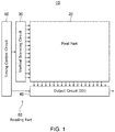
- Fig. 1 is a block diagram showing an example configuration of a solid-state imaging device according to a first embodiment of the present invention.
- the solid-state imaging device 10 is constituted by, for example, a CMOS image sensor having a digital pixel as a pixel thereof.
- the solid-state imaging device 10 is constituted mainly by a pixel part 20 serving as an image capturing part, a vertical scanning circuit (a row scanning circuit) 30, an output circuit 40, and a timing control circuit 50.
- a pixel part 20 serving as an image capturing part
- a vertical scanning circuit (a row scanning circuit) 30 serving as an image capturing part
- an output circuit 40 serving as an output circuit
- a timing control circuit 50 constitutes a reading part 60 for reading pixel signals.
- the pixel part 20 includes digital pixels, and each digital pixel includes a photoelectric conversion reading part, an analog-to-digital (AD) converting part, and a memory part.
- the solid-state imaging device 10 is configured, for example, as a stacked CMOS image sensor capable of operating in a global shutter mode.
- each digital pixel DP has an AD converting function, and the AD converting part includes a comparator for performing a comparing operation of comparing the voltage signal read out by the photoelectric conversion reading part against a referential voltage and outputting a digital comparison result signal.
- the comparator Under the control of the reading part 60, the comparator performs a first comparing operation, a second comparing operation and a third comparing operation.
- the first comparing operation is designed to output a digital first comparison result signal obtained by processing the voltage signal corresponding to the overflow charges that overflow from the photoelectric conversion element to the output node (floating diffusion) in a storing period.
- the second comparing operation is designed to output a digital second comparison result signal obtained by processing the voltage signal corresponding to the charges stored in the photoelectric conversion element that are transferred to the output node in a transfer period following the storing period.
- the third comparing operation is designed to output a digital third comparison result signal obtained by processing the voltage signal corresponding to the sum of the charges stored in the charge storing part and the charges stored in the photoelectric conversion element that are transferred to the output node in the transfer period following the storing period.
- the solid-state imaging device 10 further includes a memory control part for controlling access made to the memory part depending on a state (in the present embodiment, the level) of the comparison result signal from the comparator.
- the memory control part controls whether or not to allow writing of the data corresponding to the second comparison result signal obtained as a result of the second comparing operation into the memory part, depending on the state of the first comparison result signal obtained as a result of the first comparing operation. More specifically, the memory control part prohibits the writing of the data corresponding to the second comparison result signal obtained as a result of the second comparing operation into the memory part, if the level of the first comparison result signal obtained as a result of the first comparing operation changes from a first level to a second level in the first comparing operation period.
- the memory control part allows the writing of the data corresponding to the second comparison result signal obtained as a result of the second comparing operation into the memory part, if the level of the first comparison result signal obtained as a result of the first comparing operation stays at and does not change from the first level in the first comparing operation period.
- the memory control part relating to the present embodiment controls whether or not to allow writing of the data corresponding to the third comparison result signal obtained as a result of the third comparing operation into the memory part, depending on the state of the first comparison result signal obtained as a result of the first comparing operation and the state of the second comparison result signal obtained as a result of the second comparing operation. More specifically, the memory control part allows the writing of the data corresponding to the third comparison result signal obtained as a result of the third comparing operation into the memory part, if the level of the second comparison result signal obtained as a result of the second comparing operation stays at and does not change from the second level in the second comparing operation period.
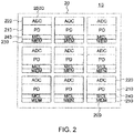
- Fig. 2 shows an example of the digital pixel array of the pixel part of the solid-state imaging device 10 relating to the first embodiment of the present invention.
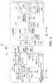
- Fig. 3 is a circuit diagram showing an example of the pixel of the solid-state imaging device 10 relating to the first embodiment of the present invention.
- a plurality of digital pixels 200 are arranged in a matrix of N rows and M columns.
- the digital pixel 200 relating to the first embodiment includes a photoelectric conversion reading part (identified as "PD” in Fig. 2 ) 210, an AD converting part (identified as “ADC” in Fig. 2 ) 220, a memory part (identified as “MEM” in Fig. 2 ) 230 and a memory control part (identified as "MCL” in Fig. 2 ) 240.
- the pixel part 20 relating to the first embodiment is configured as a stacked CMOS image sensor made up by a first substrate 110 and a second substrate 120, as will be described in detail below.
- the photoelectric conversion reading part 210 is formed in the first substrate 110
- the AD converting part 220, the memory part 230 and the memory control part 240 are formed in the second substrate 120.
- the photoelectric conversion reading part 210 of the pixel 200 includes a photodiode (a photoelectric conversion element) and an in-pixel amplifier. More specifically, the photoelectric conversion reading part 210 includes, for example, a photodiode PD1, which is a photoelectric conversion element.
- one transfer transistor TG1-Tr serving as a transferring element
- one reset transistor RST1-Tr serving as a resetting element
- one source follower transistor SF1-Tr serving as a source follower element
- one current transistor IC1-Tr serving as a current source element
- one storage transistor CG1-Tr serving as a storage capacitor element
- one floating diffusion FD1 serving as an output node ND1
- one reading node ND2 are provided.
- the photoelectric conversion reading part 210 of the digital pixel 200 relating to the first embodiment includes five transistors (5Tr), namely, the transfer transistor TG1-Tr, the reset transistor RST1-Tr, the source follower transistor SF1-Tr, the current transistor IC1-Tr and the storage transistor CG1-Tr.
- 5Tr five transistors
- the source follower transistor SF1-Tr, the current transistor IC1-Tr, and the reading node ND2 together constitute an output buffer part 211.
- the storage transistor CG1-Tr and the storage capacitor CS1 serving as a storage capacitor element together constitute a charge storing part 212.
- the reading node ND2 of the output buffer part 211 is connected to the input part of the AD converting part 220.
- the photoelectric conversion reading part 210 converts the charges in the floating diffusion FD1 serving as an output node into a voltage signal at a level corresponding to the amount of the charges and outputs the voltage signal VSL to the AD converting part 220.
- the photoelectric conversion reading part 210 outputs, in a first comparing operation period PCMPR1 of the AD converting part 220, a voltage signal VSL corresponding to the overflow charges overflowing from the photodiode PD1, which is a photoelectric conversion element, to the floating diffusion FD1 serving as an output node in a storing period PI.
- the photoelectric conversion reading part 210 outputs, in a second comparing operation period PCMPR2 of the AD converting part 220, a voltage signal VSL corresponding to the charges stored in the photodiode PD1 that are transferred to the floating diffusion FD1 serving as an output node in the transfer period PT following the storing period PI.
- the photoelectric conversion reading part 210 outputs a read-out reset signal (signal voltage) (VRST) and a read-out signal (signal voltage) (VSIG), as a pixel signal, to the AD converting part 220 in the second comparing operation period PCMPR2.
- the photoelectric conversion reading part 210 outputs, in a third comparing operation period PCMPR3 of the AD converting part 220, a voltage signal VSL corresponding to the sum of (adding together) the charges stored in the storing part 2122 and the charges stored in the photodiode PD1 that are transferred to the floating diffusion FD1 serving as an output node in the transfer period PT following the storing period PI.
- the photoelectric conversion reading part 210 outputs a read-out reset signal (signal voltage) (VRST) and a read-out signal (signal voltage) (VSIG), as a pixel signal, to the AD converting part 220 in the third comparing operation period PCMPR3.
- the photoelectric conversion reading part 210 performs a first conversion gain reset reading operation HCGRRD in a first reset period PR1 to read, from the output buffer part 211, a first read-out reset signal HCGVRST that is obtained by conversion with a first conversion gain (for example, a high conversion gain: HCG) determined by a first amount of charges at the floating diffusion FD1, which is the output node ND1.
- a first conversion gain for example, a high conversion gain: HCG
- the photoelectric conversion reading part 210 performs a first conversion gain signal reading operation HCGSRD in a reading period PRD following the transfer period PT1 after the first reset period PR1 to read, from the output buffer part 211 a first read-out signal HCGVSIG that is obtained by conversion with the first conversion gain (HCG) determined by the first amount of charges at the floating diffusion FD1, which is the output node ND1.
- HCGSRD first conversion gain signal reading operation
- the photoelectric conversion reading part 210 performs a second conversion gain signal reading operation LCGSRD to read, from the output buffer part 211, a second read-out signal LCGVSIG2 that is obtained by conversion with a second conversion gain (for example, a low conversion gain: LCG) determined by a second amount of charges equal to the sum of the charges at the storage capacitor CS1 and the charges at the floating diffusion FD1, which is the output node ND1.
- a second conversion gain for example, a low conversion gain: LCG
- the photoelectric conversion reading part 210 performs a second conversion gain reset reading operation LCGRRD in a second reset period PR2 to read, from the output buffer part 211, a second read-out reset signal LCGVRST that is obtained by conversion with a second conversion gain (LCG) determined by the second amount of charges.
- LCG conversion gain
- the solid-state imaging device 10 operates in a time stamp (TS) mode in the first comparing operation period PCMPR1 of the AD converting part 220, operates in an HCG (a first conversion gain) mode in the second comparing operation period PCMPR2, and operates in an LCG (second conversion gain) mode in the third comparing operation period PCMPR3.
- TS time stamp
- the photodiode PD1 generates signal charges (electrons) in an amount determined by the amount of the incident light and stores the same. Description will be hereinafter given of a case where the signal charges are electrons and each transistor is an n-type transistor. However, it is also possible that the signal charges are holes or each transistor is a p-type transistor. Further, this embodiment is also applicable to the case where a plurality of photodiodes and transfer transistors share the transistors.
- the photodiode (PD) in each digital pixel 200 is a pinned photodiode (PPD).
- PPD pinned photodiode
- a pinned photodiode (PPD) a charge storage part of the photodiode (PD) is pinned in the substrate to reduce mixing of the dark current into signals.
- the transfer transistor TG1-Tr of the photoelectric conversion reading part 210 is connected between the photodiode PD1 and the floating diffusion FD1 and controlled by a control signal TG applied to the gate thereof through a control line.
- the transfer transistor TG1-Tr remains selected and in the conduction state during a transfer period PT in which the control signal TG is at the high (H) level, to transfer to the floating diffusion FD1 the charges (electrons) produced by the photoelectric conversion and then stored in the photodiode PD1.
- the transfer transistor TG1-Tr After the photodiode PD1 and the floating diffusion FD1 are reset to a predetermined reset potential, the transfer transistor TG1-Tr enters the non-conduction state with the control signal TG being set to the low (L) level and the photodiode PD1 enters a storing period PI.
- the intensity of the incident light is very high (the amount of the incident light is very large)
- the charges above the amount of saturated charges overflow into the floating diffusion FD1 as overflow charges through the overflow pass under the transfer transistor TG1-Tr.
- the incident light has very high illuminance, for example, the charges above the amount of saturated charges at the floating diffusion FD1 overflow to the storage capacitor CS1 as overflow charges through the overflow pass under the storage transistor CG1-Tr.
- the reset transistor RST1-Tr is connected between the power supply line Vdd of the power supply voltage VDD and the floating diffusion FD1 and controlled by a control signal RST applied to the gate thereof through a control line.
- the reset transistor RST1-Tr remains selected and in the conduction state during a reset period in which the control signal RST is at the H level, to reset the floating diffusion FD1 to the potential of the power supply line Vdd of the power supply voltage VDD.
- the storage transistor CG1-Tr is connected between the floating diffusion FD1 and the reset transistor RST1-Tr, and the storage capacitor CS1 is connected between (i) the connection node ND3 between the floating diffusion FD1 and the reset transistor RST1-Tr and (ii) the reference potential VSS.
- the storage transistor CG1-Tr is controlled by a control signal DCG applied to the gate thereof through a control line.
- the storage transistor CG1-Tr remains selected and in the conduction state during a reset period in which the control signal DCG is at the H level so as to connect the floating diffusion FD1 and the storage capacitor CS1.
- the solid-state imaging device 10 may be also configured such that the reading part 60 may selectively connect (couple) the floating diffusion FD1 serving as an output node and the storage capacitor CS1 depending on the illuminance of the signal.
- the source follower transistor SF1-Tr serving as ae source follower element is connected at the source thereof to the reading node ND2, at the drain thereof to the power supply line Vdd, and at the gate thereof to the floating diffusion FD1.
- the drain and source of the current transistor IC1-Tr serving as a current source element are connected between the reading node ND2 and the reference potential VSS (for example, GND).
- the gate of the current transistor IC1-Tr is connected to the feeding line of a control signal VBNPIX.
- the signal line LSGN1 between the reading node ND2 and the input part of the AD converting part 220 is driven by the current transistor IC1-Tr serving as a current source element.
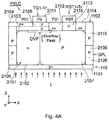
- Fig. 4A is a simplified sectional view showing an example configuration of a charge storing and transferring system or the main part of the digital pixel relating to the first embodiment of the present invention
- Fig. 4B is a potential diagram showing what happens during an overflow.
- Figs. 4A and 4B show a basic charge storing and transferring system from the photodiode PD1 to the floating diffusion FD1 and do not show the storage transistor CG1-Tr and the storage capacitor CS1 constituting the charge storing part 212 for the sake of simplicity.
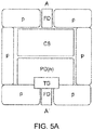
- Figs. 5A and 5B are respectively a simplified top view and a simplified sectional view showing an example configuration of the charge storing and transferring system including a storage capacitor, which is the main part of the digital pixel relating to the first embodiment of the present invention.
- Each digital pixel cell PXLC is formed on a substrate (in the present example, the first substrate 110) having a first substrate surface 1101 (for example, back surface) irradiated with light L and a second substrate surface 1102 that opposes the first substrate surface 1101 and defined by a separation layer SPL.
- the digital pixel cell PLXC shown in Fig. 4A includes the photodiode PD1, the transfer transistor TG1-Tr, the floating diffusion FD1 and the reset transistor RST1-T, which together form the photoelectric conversion reading part 210, the separation layer SPL, and a color filter part and a microlens, which are not shown.
- the photodiode PD1 includes a semiconductor layer of a first conductivity type (in the present embodiment, the n type) (in the present embodiment, the n layer) 2101 that is embedded in the semiconductor substrate having the first substrate surface 1101 and the second substrate surface 1102 opposing the first substrate surface 1101, and is capable of photoelectrically convert the received light and storing charges.
- a separation layer SPL of a second conductivity type is formed on the lateral portion of the photodiode PD1 that is positioned at the end in the direction orthogonal to the normal to the substrate (the X direction of the orthogonal coordinate system in Fig. 4A ).
- each digital pixel cell PXLC uses a pinned photodiode (PPD) as the photodiode (PD).
- PPD photodiode
- a pinned photodiode (PPD) a charge storage part of the photodiode (PD) is buried in the substrate to reduce mixing of the dark current into signals.
- the n layer (the first-conductivity-type semiconductor layer) 2101 has a two-layer structure in the normal direction to the substrate 110 (the Z direction in the orthogonal coordinate system shown in Fig. 4A ).
- an n- layer 2102 is the closest to the first substrate surface 1101 and an n layer 2103 is closer to the second substrate surface 1102 than the n- layer 2102 is, and a p+ layer 2104 and a p layer 2105 are further formed and positioned closer to the second substrate surface 1102 than the n layer 2103 is.
- a p+ layer 2106 is formed and positioned closer to the first substrate surface 1101 than the n- layer 2102 is.
- the p+ layer 2106 is formed without a gap and covers not only the photodiode PD1 but also the separation layer SPL and further other digital pixel cells PXLC.
- a color filter part is formed on the light incidence surface of the P+ layer 2106, and a microlens is further formed on the light incidence surface of the color filter part in a portion corresponding to the photodiode PD1 and a portion of the separation layer SPL.
- a single-layer structure may be employed, or a stacked structure made up by three, four or more layers may be alternatively applied.
- a first p layer (a second-conductive-type semiconductor layer) 2107 is formed on the right lateral portion of the n- layer 2102 of the photodiode PD1 in the direction orthogonal to the normal to the substrate (the X direction in the orthogonal coordinate system shown in Fig. 4A ).
- a second p layer (a second-conductivity-type semiconductor layer) 2108 is formed and has a two-layer structure in the normal direction to the substrate 110 (the Z direction in the orthogonal coordinate system shown in Fig. 4A ).
- a p- layer 2109 is closer to the first substrate surface 1101 and a p layer 2110 is closer to the second substrate surface 1102 than the p- layer 2109 is.
- a single-layer structure may be employed, or a stacked structure made up by three, four or more layers may be alternatively applied.
- the p+ layer 2106 is formed on the first p layer 2107 and the second p- layer 2109 of the p-type separation layer SPL on the first substrate surface 1101 side thereof.
- n layer 2103 is formed such that overflow pass OVP partly covers the surface of the first p layer 2107 of the p-type separation layer SPL that faces the second substrate surface 1102.
- a gate electrode 2111 of the transfer transistor TG1-Tr is formed with a gate insulator sandwiched therebetween.
- an n+ layer 2112 is formed, which is to be formed into the floating diffusion FD1
- a p layer 2113 is formed adjacent to the n+ layer 2112 which is to be formed into the channel formation region of the reset transistor RST1-Tr
- an n+ layer 2114 is formed adjacent to the p layer 2113.
- a gate electrode 2115 is formed with a gate insulator sandwiched therebetween.
- the AD converting part 220 of the digital pixel 200 compares the analog voltage signal VSL output from the photoelectric conversion reading part 210 against the referential voltage VREF, which has a ramp waveform varying with a predetermined gradient or a fixed voltage level, to convert the analog signal into a digital signal.
- the AD converting part 220 includes a comparator (COMP) 221, a counter (CNT) 222, an input-side coupling capacitor C221, an output-side load capacitor C222, and a reset switch SW-RST.
- COMP comparator
- CNT counter
- SW-RST reset switch
- a first input terminal or inversion input terminal (-) receives a voltage signal VSL fed thereto, which is output from the output buffer part 211 of the photoelectric conversion reading part 210 to the signal line LSGN1, a second input terminal or non-inversion input terminal (+) receives the referential voltage VREF fed thereto.
- the comparator 221 performs a comparing operation of comparing the voltage signal VST against the referential voltage VREF and outputting a digital comparison result signal SCMP.
- the first input terminal or inversion input terminal (-) of the comparator 221 is connected to a coupling capacitor C221.
- the output buffer part 211 of the photoelectric conversion reading part 210 formed on the first substrate 110 is AC coupled to the input part of the comparator 221 of the AD converting part 220 formed on the second substrate 120, so that the noise can be reduced and high SNR can be achieved when the illuminance is low.
- the reset switch SW-RST is connected between the output terminal and the first input terminal or inversion input terminal (-), and the load capacitor C222 is connected between the output terminal and the reference potential VSS.
- the comparator 221 compares the analog signal (the potential VSL) read from the output buffer part 211 of the photoelectric conversion reading part 210 to the signal line LSGN1 against the referential voltage VREF, for example, the ramp signal RAMP that linearly changes with a certain gradient or has a slope waveform.
- the counter 222 which is provided for each column, is operating.
- the ramp signal RAMP having a ramp waveform and the value of the counter vary in a one-to-one correspondence, so that the voltage signal VSL is converted into a digital signal.
- the AD converting part 220 converts a change in voltage, in other words, a change in the referential voltage VREF (for example, the ramp signal RAMP) into a change in time, and converts the change in time into a digital value by counting the change in time at certain intervals (with certain clocks).
- the analog signal VSL and the ramp signal RAMP the referential voltage VREF
- the output from the comparator 221 is inverted and the clock input into the counter 222 is stopped, or the suspended clock is input into the counter 222 and the value (data) of the counter 222 at that timing is saved in the memory part 230. In this way, the AD conversion is completed.
- the data (signal) stored in the memory part 230 of each digital pixel 200 is output through the output circuit 40 to a signal processing circuit (not shown) and subject to predetermined signal processing, so that a two-dimensional image is produced.
- the comparator 221 of the AD converting part 220 of the first embodiment is driven and controlled by the reading part 60 to perform first and second comparing operations and a third comparing operation during a pixel signal reading period.
- the comparator 221 When performing the first comparing operation CMPR1, under the control of the reading part 60, the comparator 221 outputs a digital first comparison result signal SCMP1 obtained by processing a voltage signal VSL1 corresponding to the overflow charges overflowing from the photodiode PD1, which is a photoelectric conversion element, to the floating diffusion FD1, which is an output node, in the storing period PI.
- the first comparing operation CMPR1 may be referred to as a TS mode or time stamp ADC mode operation.
- the comparator 221 When performing the second comparing operation CMPR2, under the control of the reading part 60, the comparator 221 outputs a digital second comparison result signal SCMP2 obtained by processing a voltage signal VSL2 (VSIG) corresponding to the charges stored in the photodiode PD1 that are transferred to the floating diffusion FD1, which is an output node, in the transfer period PT following the storing period PI.
- a voltage signal VSL2 (VRST) corresponding to the reset voltage in the floating diffusion FD1 at the time of resetting is converted into a digital signal.
- the second comparing operation CMPR2 may be referred to as an HCG mode or linear ADC mode operation.
- a digital third comparison result signal SCMP3 is output, which is obtained by processing a voltage signal VSL3 (VSIG) corresponding to the sum of (adding together) the charges stored in the charge storing part 212 and the charges stored in the photodiode PD1 that are transferred to the floating diffusion FD1 serving as an output node in the transfer period PT following the storing period PI.
- a voltage signal VSL3 (VRST) corresponding to the reset voltage in the floating diffusion FD1 at the time of resetting is converted into a digital signal.
- the third comparing operation CMPR3 may be referred to as an LCG mode or linear ADC mode operation.
- the storing period PI basically denotes the period from when the photodiode PD1 and the floating diffusion FD1 are reset to the reset level to when the transfer transistor TG1-Tr is switched to the conduction state and the transfer period PT starts.
- the period PCMPR1 for the first comparing operation CMPR1 denotes the period from when the photodiode PD1 and the floating diffusion FD1 are reset to the reset level to when the first comparing operation CMPR1 ends before the transfer period PT starts.
- the period PCMPR2 for the second comparing operation CMPR2 denotes the period including the period after the transfer period PT, in which the reset level is sampled at the comparator 221 after the storing period PI ends.
- the period PCMPR3 for the third comparing operation CMPR3 denotes the period in which the stored charges are sampled at the comparator 221 as the referential voltage and the reset level is subsequently sampled.
- Fig. 6 is used to illustrate the first comparing operation CMPR1 performed by the comparator 221 relating to the first embodiment of the present invention.
- the horizontal axis represents the time and the vertical axis represents the voltage level VFD of the floating diffusion FD1, which is an output node.
- the referential voltage VREF1 for the comparator 221 is set to voltage VREFsat, which is a fixed level observed at the timing of non-saturation before the saturation is reached, or set to ramp voltage VREFramp, which varies from the voltage level VREFrst at the timing of resetting to the voltage level VREFsat.
- the referential voltage VREF1 is set to the level VREFsat or VREFramp during the first comparing operation CMPR1, the time required to flip (invert) the output of the comparator 221 decreases as the intensity of the incident light or illuminance increases as shown in Fig. 6 . This is because the amount of charges increases as the intensity of the incident light or illuminance increases.
- the output of the comparator 221 is flipped (inverted) immediately at a timing t1 from a first level (for example, the Low level) to a second level (the High level).
- the output of the comparator 221 is flipped (inverted) at a timing t2 later than the timing t1 from the first level (for example, the Low level) to the second level (the High level).
- the output of the comparator 221 is flipped(inverted) at a timing t3 later than the timing t2 from the first level (for example, the Low level) to the second level (the High level).
- the comparator 221 outputs the first comparison result signal SCMP1 corresponding to the time determined by the amount of the overflow charges from the photodiode PD1 to the floating diffusion FD1 in a predetermined period of time within the storing period PI.
- the comparator 221 is capable of comparing the light level against the referential voltage as long as the light level produces the signal level ranging (i) from the signal level corresponding to a predetermined threshold value of the photodiode PD1 obtained with a maximum value of the sampling time that is required to cause the overflow charges to start overflowing from the photodiode PD1 to the floating diffusion FD1, which is an output node, (ii) to the signal level obtained with a minimum value of the sampling time.
- the photo conversion operation in the time stamp ADC mode involves light to time conversion in the storing period PI.
- the output of the comparator 221 is flipped from the first level (for example, the Low level) to the second level (the High level) immediately after the reset activation period, and this light level corresponds to a saturation signal (a well capacity) described as the following equation.
- the FD saturation amount is 8 Ke-at 150 uV/e- (the FD capacitance of 1.1fF)
- the minimum sampling time is 15 nsec
- the storing time is 3 msec.
- This time stamp ADC operation mode (or the TS mode) is, as described above, capable of comparing the light level against the reference level as long as the light level produces the signal level ranging (i) from the signal level corresponding to a predetermined threshold value of the photodiode PD1 obtained with a maximum value of the sampling time that is required to cause the overflow charges to start overflowing from the photodiode PD1 to the floating diffusion FD1, which is an output node, (ii) to the signal level obtained with a minimum value of the sampling time.
- Fig. 7 is used to illustrate the first comparing operation CMPR1 performed by the comparator 221 relating to the first embodiment and shows other examples of the pattern of the referential voltage.
- the referential voltage VREF may be a voltage signal having a ramp waveform (signal) RAMP that varies with a predetermined gradient indicated by the number (1) in Fig. 7 , a voltage signal having a fixed voltage DC indicated by the number (2) in Fig. 7 , a log voltage signal indicated by the number (3) in Fig. 7 or an exponential voltage signal indicated by the number (4) in Fig. 7 .
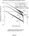
- Fig. 8 shows the result of the light to time conversion when the referential voltage VREF input into the comparator relating to the first embodiment is varied in level.
- the horizontal axis represents the sampling time
- the vertical axis represents the estimated signal in the overflow signal.
- the overflow signal means the estimated result under such a condition that the transfer transistor TG1-Tr is in the conduction state and the photodiode PD1 stores no charges (non-overflow).
- Fig. 8 shows a sampling time required to flip the output of the comparator 221 corresponding to the overflow charges (signal) for different natures (properties) of the applied light.
- Fig. 8 shows the sampling time required to flip for various fixed reference voltage levels DC1, DC2, DC3 and a ramp reference voltage VRAMP. In this example, a linear reference ramp is used.
- the floating diffusion FD1 and the comparator 221 are reset, and the linear ADC mode (HCG mode) subsequently starts, in which the second comparing operation CMPR2 for the non-saturated charges is performed. Further later, the linear ADC mode (LCG mode) starts in which the third comparing operation CMPR3 for the saturated charges is performed.
- Fig. 9 shows the photo response coverage relating to the first comparing operation and the second comparing operation performed in the digital pixel relating to the first embodiment of the present invention.
- “A” represents the signal (AD conversion transfer curve) obtained in the time stamp ADC mode operation and "B” represents the signal (AD conversion transfer curve) obtained in the linear ADC mode (HCG mode).
- Fig. 10 shows the photo response coverage (photo conversion plot) relating to first and second comparing operations, and a third comparing operation performed in the digital pixel relating to the first embodiment of the present invention.
- Fig. 9 shows the photo response coverage relating to the first comparing operation and the second comparing operation performed in the digital pixel relating to the first embodiment of the present invention.
- FIG. 10 “A” represents the signal (AD conversion transfer curve) obtained in the time stamp ADC mode operation, “B” represents the signal (AD conversion transfer curve) obtained in the linear ADC mode (HCG mode), and “C” represents the signal (AD conversion transfer curve) obtained in the linear ADC mode (LCG mode).
- the horizontal axis represents the light intensity, and the vertical axis represents the total amount Qp of the electrons obtained by photo conversion.
- Figs. 11A and 11B are potential diagrams for signal charges in the cases of LCG and HCG.
- the time stamp ADC mode (or TS mode) can provide photo response for very bright light
- the linear ADC mode can provide photo response for dark light.
- a dynamic range of 120 dB can be realized.
- the saturation signal within the photo conversion range has 900 Ke, as described above. Since the linear ADC mode involves a normal reading operation employing ADC, the linear ADC mode can cover the range from 2e or the noise level to 8Ke where the photodiode PD1 and the floating diffusion FD1 are saturated.
- the coverage provided by the linear ADC mode can be increased to 30 Ke by adding a switch and a capacitor.
- images can be obtained from light having a wide range of illuminance levels from low illuminance to high illuminance.
- the single-exposure dynamic range can be widened, global reading can be realized without pixel distortion, random access or ADC conversion in each pixel can be performed, and linearity can be reliably achieved in the high-illuminance region.
- the SN may disadvantageously get worse due to insufficient resolution of the digital signal.
- the signal (AD conversion transfer curve) obtained in the linear ADC mode (LCG mode) C exists between the signal (AD conversion transfer curve) A obtained in the time stamp ADC mode and the signal (AD conversion transfer curve) B obtained in the linear ADC mode (HCG mode).
- the signal (AD conversion transfer curve) B obtained in the linear ADC mode (HCG mode) and the signal (AD conversion transfer curve) C obtained in the linear ADC mode operation (LCG mode) overlap in the mode transition region MOR.
- images can be obtained from light having a wide range of illuminance levels from low illuminance to high illuminance.
- the single-exposure dynamic range can be widened, global reading can be realized without pixel distortion, random access or ADC conversion in each pixel can be performed, and linearity can be reliably achieved in the high- and low-illuminance regions.
- Fig. 12 shows the photo response coverages (photo conversion plots) relating to the first and second comparing operations performed in the digital pixel relating to the first embodiment of the present invention and the third comparing operation, and shows how the light intensity is related to the total amount Qp of the electrons obtained by the photo conversion.
- Fig. 13 shows the photo response coverages (photo conversion plots) relating to the first and second comparing operations and the third comparing operation performed in the digital pixel relating to the first embodiment of the present invention and shows how the light intensity is related to the ADC code.
- Fig. 12 shows the photo response coverages (photo conversion plots) relating to the first and second comparing operations performed in the digital pixel relating to the first embodiment of the present invention and the third comparing operation, and shows how the light intensity is related to the ADC code.
- FIG. 14 shows the photo response coverages (photo conversion plots) relating to the first and second comparing operations and the third comparing operation performed in the digital pixel relating to the first embodiment of the present invention and shows how the light intensity is related to the memory code.
- Fig. 15 shows the photo response coverages (photo conversion plots) relating to the first and second comparing operations and the third comparing operation performed in the digital pixel relating to the first embodiment of the present invention, and shows how the light intensity is related to the SNR.
- the signal (AD conversion transfer curve) C obtained in the linear ADC mode exists between the signal (AD conversion transfer curve) A obtained in the time stamp ADC mode and the signal (AD conversion transfer curve) B obtained in the linear ADC mode (HCG mode), as shown in Fig. 10 .
- Fig. 16 is used to illustrate the configuration and function of the memory part and the memory control part relating to the first embodiment of the present invention.
- the memory part 230 includes a first memory (Mem1) 231 and a second memory (Mem2) 232 as shown in Figs. 3 and 12 .
- the first memory 231 saves, under the control of the memory control part 240, the first comparison result signal SCMP1, the second comparison result signal SCMP2 and the third comparison result signal SCMP3 from the comparator 221 in the form of n-bit digital data.
- the second memory 232 saves, under the control of the memory control part 240, status information indicative of the operational mode.
- the second memory 232 saves, for example, status information of "0" for the HCG mode, status information "2" for the LCG mode, and status information "1" for the TS mode.
- Fig. 17 shows, as an example, status information indicating the operational mode stored in the second memory 232 in association with various levels of light intensity in the first embodiment.
- the responsiveness is 100 Ke/lux
- the amount of charges Qpd in the photodiode PD1 is 2 Ke
- the amount of charges Qfd in the floating diffusion FD1 is 62 Ke
- the storing time (Tint)/the sampling time (Tsample) is 400 ⁇ s/1.56 ⁇ s
- the bit depth of the first memory 231 is 8 bits.
- the light level is low.
- the light intensity range [lux] is lower than -5 e2
- the amount of charges Qpd in the photodiode PD1 is lower than 2 Ke
- the amount of charges Qfd in the floating diffusion FD1 is zero
- the total maximum amount of charges Qmax is 2 Ke.
- the first memory 231 saves the second comparison result signal SCMP2 provided from the comparator 221 in the form of n-bit digital data corresponding to "0-255.”
- the light level is middle.
- the light intensity range [lux] is within the range of -5 e2 to 1.6 e4
- the amount of charges Qpd in the photodiode PD1 is larger than 2 Ke
- the amount of charges Qfd in the floating diffusion FD1 is smaller than 62 Ke
- the total maximum amount of charges Qmax is smaller than 62 Ke.
- the first memory 231 saves the third comparison result signal SCMP3 provided from the comparator 221 in the form of n-bit digital data corresponding to "0-255.”
- the light level is high.
- the light intensity range [lux] is within the range of 1.6 e4 to 4 e6
- the amount of charges Qpd in the photodiode PD1 is larger than 2 Ke
- the amount of charges Qfd in the floating diffusion FD1 is smaller than 62 Ke
- the total maximum amount of charges Qmax is smaller than 15872 Ke.
- the first memory 231 saves the first comparison result signal SCMP1 provided from the comparator 221 in the form of n-bit digital data corresponding to "0-255.”
- the memory control part 240 includes a writing control part (write controller (WC)) 241 for the memory part 230.
- the writing control part 241 monitors whether the output from the comparator 221 is inverted to the level “1" or remains at the level “0" without being inverted, and allows the writing into the first memory 231 and the second memory 232 (write enable) unless the comparator 221 outputs the level "0.”
- the memory control part 240 controls whether to allow the writing of the data corresponding to the second comparison result signal SCMP2 obtained as a result of the second comparing operation CMPR2 into the memory part 230, depending on the state of the first comparison result signal SCMP1 obtained as a result of the first comparing operation CMPR1.
- the memory control part 240 controls whether to allow the writing of the data corresponding to the third comparison result signal SCMP3 obtained as a result of the third comparing operation CMPR3 into the memory part 230, depending on the state of the first comparison result signal SCMP1 obtained as a result of the first comparing operation CMPR1 and the state of the second comparison result signal SCMP2 obtained as a result of the second comparing operation CMPR2.
- Fig. 18 shows an example configuration of the first memory and an output circuit of the memory part relating to the first embodiment of the present invention.
- the n-bit memory 231 saves, in the form of digital data, the first comparison result signal SCMP1 that is obtained as a result of the first comparing operation CMPR1 in the comparator 221 by digitizing the voltage signal corresponding to the overflow charges in the floating diffusion FD1, the second comparison result signal SCMP2 obtained as a result of the second comparing operation CMPR2 by digitizing the charges stored in the photodiode PD1 and the third comparison result signal SCMP3 obtained as a result of the third comparing operation CMPR3 by digitizing the sum of the charges stored in the photodiode PD1 and the charges stored in the charge storing part 212, in a correlative manner.
- the first memory 231 which is capable of sampling and holding n-bit data, is formed by SRAM, DRAM and the like, receives, for example, digitized signals fed thereto, is compatible with photo conversion codes, and can be read by an external IO buffer 41 in the output circuit 40 near the pixel array.
- the memory control part 240 controls whether to allow memory access to the first memory 231, to be more specific, whether to allow writing (overwriting), using the output signal S241 from the memory control part 240, depending on the state (in the present embodiment, the level) of the comparison result signal output from the comparator 221. If the signal S241 corresponding to the first comparison result signal SCMP1 obtained as a result of the first comparing operation CMPR1 is fed at a first level (the Low level), the writing (overwriting) to the first memory 231 is prohibited. If the signal S241 is fed at a second level (the High level), the writing (overwriting) is allowed.
- the first memory 231 is controlled by the memory control part 240 as to whether writing of the data corresponding to the third comparison result signal obtained as a result of the third comparing operation into the first memory 231 is to be performed, depending on the state of the first comparison result signal obtained as a result of the first comparing operation and the state of the second comparison result signal obtained as a result of the second comparing operation.
- the memory control part 240 allows writing (overwriting) of the data corresponding to the third comparison result signal SCMP3 obtained as a result of the third comparing operation CMPR3 into the first memory 231 if the level of the second comparison result signal SCMP2 obtained as a result of the second comparing operation CMPR2 stays at and does not change from the second level (the High level) in the second comparing operation period PCMPR2.
- Fig. 19 is a flowchart illustrating a sequence of operations performed in a reading mode by the memory control part and the memory part of the solid-state imaging device relating to the first embodiment of the present invention.
- the reading mode enters the TS mode (ST1) and the first comparing operation CMPR1 is performed. Accordingly, the first memory 231 and the second memory 232 are reset (ST11, ST21).
- the memory control part 240 judges whether the output from the comparator 221 as a result of the first comparing operation CMPR1 is flipped (inverted) from the first level (Low level) to the second level (High level) (ST2).
- the step ST2 judges that the output from the comparator 221 is flipped, the first comparison result signal SCMP1 obtained in the first comparing operation CMPR1 by digitizing the voltage signal corresponding to the overflow charges in the floating diffusion FD1 is written into the first memory 231 in the form of an ADC code, which is a digital code (ST12).
- the writing allowed (write enable) signal is locked (ST31).
- step ST2 judges that the output from the comparator 221 is not flipped, the reading mode is updated from the TS mode to the HCG mode, the reference voltage VREF having a ramp waveform is reset (ST3), and the status information in the second memory 232 is updated from "1" indicating the TS mode to "0" indicating the HCG mode (ST22).
- the second comparing operation CMPR2 is performed. This involves resetting the first memory 231 (ST13).
- the memory control part 240 judges whether the output from the comparator 221 as a result of the second comparing operation CMPR2 is flipped (inverted) from the first level (Low level) to the second level (High level) (ST5).
- the step ST5 judges that the output from the comparator 221 is flipped, the second comparison result signal SCMP2 obtained as a result of the second comparing operation CMPR2 by digitizing the voltage signal corresponding to the charges stored in the photodiode PD1 is written into the first memory 231 in the form of an ADC code, which is digital data (ST14).
- the writing allowed (write enable) signal is locked (ST32).
- step ST5 judges that the output from the comparator 221 is not flipped, the reading mode is updated from the HCG mode to the LCG mode, the reference voltage VREF having a ramp waveform is reset (ST6), and the status information in the second memory 232 is updated from "0" indicating the HCG mode to "2" indicating the LCG mode (ST23).
- the third comparing operation CMPR3 is performed. This involves resetting the first memory 231 (ST15).
- the memory control part 240 judges whether the output from the comparator 221 as a result of the third comparing operation CMPR3 is flipped (inverted) from the second level (High level) to the first level (Low level) (ST8).
- the step ST8 judges that the output from the comparator 221 is flipped, the third comparison result signal SCMP3 obtained as a result of the third comparing operation CMPR3 by digitizing the voltage signal corresponding to the sum of the charges stored in the photodiode PD1 and the charges stored in the charge storing part 212 is written into the first memory 231 in the form of an ADC code, which is digital data (ST16).
- the writing allowed (write enable) signal is locked (ST33).
- Fig. 20 is a flowchart illustrating a sequence of operations performed by the memory part of the solid-state imaging device relating to the first embodiment of the present invention.
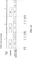
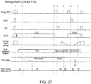
- Fig. 21 shows an example sequence of operations performed in a frame reading scheme by the solid-state imaging device 10 relating to the first embodiment of the present invention.
- the following first describes an example of the frame reading scheme in the solid-state imaging device 10.
- TS denotes the period in which the operations of the time stamp ADC or TS mode are performed
- H denotes the period in which the operations of the HCG mode are performed
- L denotes the period in which the operations of the LCG mode are performed.
- the overflow charges are stored in the floating diffusion FD1 in the storing period PI.
- the solid-state imaging device 10 operates in the time stamp ADC mode or TS mode within the storing period PI. Actually, the solid-state imaging device 10 operates in the TS mode within a period that is included in the storing period PI and lasts until the floating diffusion FD1 is reset. On completion of the operations in the TS mode, the solid-state imaging device 10 transitions to the linear ADC mode (HCG mode), so that the signal (VRST) at the floating diffusion FD1 at the time of resetting is read and converted into a digital signal to be stored in the memory part 230.
- HCG mode linear ADC mode
- the signal (VSIG) corresponding to the charges stored in the photodiode PD1 is read and converted into a digital signal to be stored into the memory part 230.
- the voltage signal VSL corresponding to the overflow charges overflowing from the photodiode PD1, which is a photoelectric conversion element, to the floating diffusion FD1, which is an output node, in the storing period PI is output.
- the voltage signal VSL corresponding to the charges stored in the photodiode PD1 that are transferred to the floating diffusion FD1 serving as an output node in the transfer period PT following the storing period PI is output.
- the read-out reset signal (signal voltage) (VRST) and the read-out signal (signal voltage) (VSIG) are output, as a pixel signal, to the AD converting part 220.
- the voltage signal VSL corresponding to the sum of (adding together) the charges stored in the photodiode PD1 that are transferred to the floating diffusion FD1 serving as an output node in the transfer period PT following the storing period PI and the charges stored in the storing part 2122 is output.
- the read-out reset signal (signal voltage) (VRST) and the read-out signal (signal voltage) (VSIG) are output, as a pixel signal, to the AD converting part 220.
- the read frame is sent outside of the solid-state imaging device 10 (the image sensor) via the IO buffer 41 ( Fig. 18 ) of the output circuit 40, which is driven by reading the digital signal data from the memory node and has such an MIPI data format.
- This operation can be globally performed in the pixel array.
- the reset transistor RST1-Tr and the transfer transistor TG1-Tr are used to reset the photodiode PD1 concurrently in all of the pixels, so that exposure to light starts concurrently in parallel in all of the pixels.
- the transfer transistor TG1-Tr is used to sample the output signal from the photoelectric conversion reading part 210 in the AD converting part 220 and the memory part 230, so that the exposure ends concurrently in parallel in all of the pixels. This successfully accomplish a perfect electronic shutter.
- the solid-state imaging device 10 relating to the present embodiment further includes the memory control part 240 for controlling access made to the memory part depending on the state (in the present embodiment, the level) of the comparison result signal from the comparator 221.
- the memory control part 240 controls whether to allow the writing of the data corresponding to the second comparison result signal SCMP2 obtained as a result of the second comparing operation CMPR2 into the memory part 230, depending on the state (the output level) of the first comparison result signal SCMP1 obtained as a result of the first comparing operation CMPR1.
- the memory control part 240 prohibits the writing of the data corresponding to the second comparison result signal SCMP2 obtained as a result of the second comparing operation CMPR2 into the memory part 230 if the level of the first comparison result signal SCMP1 obtained as a result of the first comparing operation CMPR1 changes from the first level (for example, Low level) to the second level (High level) in the first comparing operation period PCMPR1.
- the memory control part 240 allows the writing of the data corresponding to the second comparison result signal SCMP2 obtained as a result of the second comparing operation CMPR2 into the memory part 230 if the level of the first comparison result signal SCMP1 obtained as a result of the first comparing operation CMPR1 stays at and does not change from the first level (for example, Low level) in the first comparing operation period PCMPR1. Furthermore, the memory control part 240 controls whether to allow writing of the data corresponding to the third comparison result signal obtained as a result of the third comparing operation into the first memory 231, depending on the state of the first comparison result signal obtained as a result of the first comparing operation and the state of the second comparison result signal obtained as a result of the second comparing operation.
- the memory control part 240 allows the writing (overwriting) of the data corresponding to the third comparison result signal SCMP3 obtained as a result of the third comparing operation CMPR3 into the first memory 231 if the level of the second comparison result signal SCMP2 obtained as a result of the second comparing operation CMPR2 stays at and does not change from the second level (for example, High level) in the second comparing operation period PCMPR2.
- the reason why the memory control part 240 is provided is described in the following.
- the fact that the level of the first comparison result signal SCMP1 obtained as a result of the first comparing operation CMPR1 changes from a first level (for example, the low level) to a second level (the High level) in the first comparing operation period PCMPR1 during the time stamp ADC mode means the following.
- the photodiode PD1 is irradiated with light having very (extremely) high illuminance (bright) and the charges obtained by the photoelectric conversion overflow from the photodiode PD1 to the floating diffusion FD1 as overflow charges. This indicates that the read-out signal in the subsequent linear ADC mode is not necessary.
- the memory control part 240 prohibits the writing (overwriting) of the data corresponding to the second comparison result signal SCMP2 obtained as a result of the second comparing operation CMPR2 into the memory part 230.
- the fact that the level of the first comparison result signal SCMP1 obtained as a result of the first comparing operation CMPR1 does not change from the first level (for example, Low level) to the second level (High level) in the first comparing operation period PCMPR1 during the time stamp ADC mode means the following.
- the photodiode PD1 is irradiated with dark light having normal or low to middle illuminance and there is a very low possibility that the charges obtained by the photoelectric conversion overflow from the photodiode PD1 to the floating diffusion FD1 as overflow charges. This indicates that the read-out signal in the subsequent linear ADC mode is necessary.
- the memory control part 240 allows the writing (overwriting) of the data corresponding to the second comparison result signal SCMP2 obtained as a result of the second comparing operation CMPR2 into the memory part 230.
- the fact that the level of the second comparison result signal SCMP2 obtained as a result of the second comparing operation CMPR2 does not change from the first level (for example, Low level) to the second level (High level) in the second comparing operation period PCMPR2 during the linear ADC mode means the following.
- the photodiode PD1 is irradiated with dark light having low to middle illuminance and there is a low possibility that the charges obtained by the photoelectric conversion overflow from the photodiode PD1 to the floating diffusion FD1 as overflow charges. This indicates that the read-out signal in the subsequent LCG mode is necessary.
- the memory control part 240 allows the writing (overwriting) of the data corresponding to the third comparison result signal SCMP3 obtained as a result of the third comparing operation CMPR3 into the memory part 230.
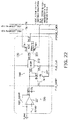
- Fig. 22 is used to illustrate an example configuration of the main parts of the memory control part 240 relating to the first embodiment of the present invention.
- Fig. 23 is a timing chart for illustrating operations performed by the memory control part when the output from the comparator is inversed in the time stamp ADC mode.
- Fig. 24 is a timing chart for illustrating operations performed by the memory control part when the output from the comparator is not inversed in the time stamp ADC mode.
- the memory control part 240 shown in Fig. 22 includes a flag bit memory cell (Flag) 241 and a NOR circuit 242, which serves as a gate circuit.
- Flag flag bit memory cell
- NOR circuit 242 which serves as a gate circuit.
- the flag bit memory cell 241 receives a flag sampling signal FLG_SAMP and the first comparison result signal SCMP1 obtained as a result of the first comparing operation CMPR1 fed thereto.
- the flag bit memory cell 241 sets a signal SA to the second level (High level) and outputs the resulting signal SA to the NOR circuit 242 if the level of the first comparison result signal SCMP1 obtained as a result of the first comparing operation CMPR1 has changed from the first level (Low level) to the second level (High level).
- the flag bit memory cell 241 When receiving the flag sampling signal FLG_SAMP fed thereto after the end of the first comparing operation period PCMPR1, the flag bit memory cell 241 sets the signal SA to the first level (Low level) and outputs the resulting signal SA to the NOR circuit 242 if the level of the first comparison result signal SCMP1 obtained as a result of the first comparing operation CMPR1 has not changed from the first level (Low level) to the second level (High level).
- the NOR circuit 242 receives the output signal SA from the flag bit memory cell 241 and the first comparison result signal SCMP1 obtained as a result of the first comparing operation CMPR1 fed thereto.
- the NOR circuit 242 sets a signal SB to the first level (Low level) and outputs the resulting signal SB to the memory part 230 so that the writing (overwriting) is prohibited.
- the NOR circuit 242 sets the signal SB to the second level (High level) and outputs the resulting signal SB to the memory part 230 so that the writing (overwriting) is allowed.
- the flag bit memory cell 241 constitutes part of the ADC memory 231. This means no overhead from the perspective of the layout and high area efficiency.
- the NOR circuit 242 can be constituted by four transistors (4T). This means minimum area overhead.
- the output signal SA from the flag bit memory cell 241 at the second level (High level) is input into the NOR circuit 242 if the level of the first comparison result signal SCMP1 obtained as a result of the first comparing operation CMPR1 has changed from the first level (Low level) to the second level (High level). Accordingly, the NOR circuit 242 sets the signal SB to the first level (the Low level) and outputs the resulting signal SB to the memory part 230, so that the writing (overwriting) is prohibited.
- the NOR circuit 242 sets the signal SB to the second level (the High level) and outputs the resulting signal SB to the memory part 230, so that the writing (overwriting) is allowed.
- the flag bit memory cell 241 and the NOR circuit 242 are cleared to the initial state by a clear signal FLG_CLR after the end of the second comparing operation period PCMPR2 performed in the linear ADC mode.
- the vertical scanning circuit 30 drives the photoelectric conversion reading part 210 of the digital pixel 200 through row-scanning control lines in shutter and reading rows, under the control of the timing control circuit 50.
- the vertical scanning circuit 30 feeds referential voltage levels VREF1, VREF2, VREF3 that are set in accordance with the first, second and third comparing operations CMPR1, CMPR2 and CMPR3, to the comparator 221 of each digital pixel 200, under the control of the timing control circuit 50. Further, the vertical scanning circuit 30 outputs, according to an address signal, row selection signals indicating the row addresses of the reading row from which signals are to be read out and the shutter row in which the charges stored in the photodiodes PD are to be reset.
- the output circuit 40 includes, as shown in, for example, Fig. 18 , an IO buffer 41 arranged in correspondence with the output from the memory in each of the digital pixels 200 in the pixel part 20 and outputs the digital data read from each digital pixel 200 to outside.
- the timing control circuit 50 generates timing signals required for signal processing in the pixel part 20, the vertical scanning circuit 30, the output circuit 40, and the like.
- the reading part 60 controls the reading of the pixel signal from the digital pixel 200 in, for example, the global shutter mode.
- the reading part 60 can also control the connection (coupling) between the floating diffusion FD1, which serves as an output node, and the storage capacitor CS1, which stores charges from the floating diffusion FD1 through the storage transistor CG1-Tr, such that the connection (coupling) may be provided selectively depending on the signal illuminance.
- the following describes the stacked structure of the solid-state imaging device 10 relating to the first embodiment.
- Figs. 25A and 25B are schematic views to illustrate the stacked structure of the solid-state imaging device 10 relating to the first embodiment.
- Fig. 26 is a simplified sectional view to illustrate the stacked structure of the solid-state imaging device 10 relating to the first embodiment.
- the solid-state imaging device 10 relating to the first embodiment has a stacked structure of a first substrate (an upper substrate) 110 and a second substrate (a lower substrate) 120.
- the solid-state imaging device 10 is formed as an imaging device having a stacked structure that is obtained, for example, by bonding wafers together and subjecting the bonded wafers to dicing.
- the first substrate 110 and the second substrate 120 are stacked.
- the photoelectric conversion reading parts 210 of the digital pixels 200 of the pixel part 20 are arranged and centered around the central portion of the first substrate 110.
- the photodiode PD is formed on a first surface 111 side thereof onto which light L is incident.
- a microlens MCL and a color filter are formed on the light incident surface of the photodiode PD.
- the transfer transistor TG1-Tr, the reset transistor RST1-Tr, the storage transistor CG1-Tr, the source follower transistor SF1-Tr, and the current transistor IC1-Tr are formed on a second surface side thereof.
- the photoelectric conversion reading parts 210 of the digital pixels 200 are arranged in a matrix pattern in the first substrate 110.
- the AD converting parts 220, memory parts 230, memory control parts 240 of the digital pixels 200 are arranged in a matrix pattern.
- the vertical scanning circuit 30, output circuit 40 and timing control circuit 50 may be also formed.
- the reading nodes ND2 of the photoelectric conversion reading parts 210 in the first substrate 110 are electrically connected to the inversion input terminals (-) of the comparators 221 of the digital pixels 200 in the second substrate 120 through vias (die-to-die vias), microbumps BMP, the signal lines LSGN1 or the like as shown in Fig. 3 , for example. Furthermore, in the present embodiment, the, the reading nodes ND2 of the photoelectric conversion reading parts 210 in the first substrate 110 are AC coupled to the inversion input terminals (-) of the comparators 221 of the digital pixels 200 in the second substrate 120 through the coupling capacitors C221.
- Fig. 27 is a timing chart to illustrate a reading operation performed by the solid-state imaging device relating to the first embodiment of the present invention in a predetermined shutter mode.
- Fig. 28 includes parts (A) to (G) illustrating a sequence of operations and potential transition to explain a reading operation performed mainly by the pixel part of the solid-state imaging device relating to the first embodiment of the present invention in a predetermined shutter mode.
- Fig. 29 includes parts (A) to (H) illustrating a sequence of operations and potential transition, including the photodiode in the non-saturated or saturated state, in a reading operation performed mainly by the pixel part of the solid-state imaging device relating to the first embodiment of the present invention in a predetermined shutter mode.
- the parts (A) to (D) show how the potential transitions in the non-saturated state
- the parts (E to (H) shows how the potential transitions in the saturated state.
- the storage transistor CG1-Tr remains in the non-conduction state for a predetermined period of time for the global resetting and reset sampling. Following this, as shown in Fig. 27 and the part (C) in Fig. 28 , the reset transistor RST1-Tr and the transfer transistor TG1-Tr are brought into the non-conduction state and the storage transistor CG1-Tr is brought into the conduction state at the same time in all of the pixels, so that the exposure is started, in other words, the charges start to be stored in all of the pixels concurrently in parallel.
- the time stamp (TS) ADC mode operation for the overflow charges starts.
- the overflow charges are stored in the floating diffusion FD1 in the storing period PI.
- the time stamp ADC mode lasts for the storing period PI, more specifically, for a period within the storing period PI until the comparing operation is completed.
- the photoelectric conversion reading part 210 outputs, correspondingly to the first comparing operation period PCMPR1 of the AD converting part 220, the voltage signal VSL1 corresponding to the overflow charges overflowing from the photodiode PD1 to the floating diffusion FD1 serving as an output node in the storing period PI.
- the comparator 221 of the AD converting part 220 performs the first comparing operation CMPR1.
- the comparator 221 Under the control of the reading part 60, the comparator 221 outputs the digital first comparison result signal SCMP1 obtained by processing the voltage signal VSL1 corresponding to the overflow charges overflowing from the photodiode PD1 to the floating diffusion FD1 serving as an output node within a certain period that is included in the storing period PI and lasts until the comparing operation is completed, and digital data corresponding to the first comparison result signal SCMP1 is stored in the memory 231 of the memory part 230.
- the reset period PR2 the reset transistor RST1-Tr remains in the non-conduction state for a predetermined period of time, so that the floating diffusion FD1 is reset.
- the signal (VRST) in the floating diffusion is read out, and the digital signal is stored in the memory 231 in the memory part 230.
- the storing period PI ends and the transfer period PT starts.
- the transfer transistor TG1-Tr remains in the conduction state for a predetermined period of time, so that the charges stored in the photodiode PD1 are transferred to the floating diffusion FD1.
- the photoelectric conversion reading part 210 outputs, correspondingly to the second comparing operation period PCMP2 of the AD converting part 220, the voltage signal VSL2 corresponding to the stored charges transferred from the photodiode PD1 to the floating diffusion FD1 serving as an output node, after the storing period PI ends.
- the solid-state imaging device 10 is in the HCG mode, and the storage transistor CG1-Tr remains in the non-conduction state.
- the comparator 221 of the AD converting part 220 performs the second comparing operation CMPR2.
- the comparator 221 Under the control of the reading part 60, the comparator 221 outputs the digital second comparison result signal SCMP2 obtained by processing the voltage signal VSL2 corresponding to the stored charges transferred from the photodiode PD1 to the floating diffusion FD1 serving as an output node, after the storing period PI, and digital data corresponding to the second comparison result signal SCMP2 is stored in the memory 231 of the memory part 230.
- the memory control part 240 controls whether to allow the writing of the data corresponding to the second comparison result signal SCMP2 obtained as a result of the second comparing operation CMPR2 into the memory part 230, depending on the state (the output level) of the first comparison result signal SCMP1 obtained as a result of the first comparing operation CMPR1.
- the memory control part 240 prohibits the writing of the data corresponding to the second comparison result signal SCMP2 obtained as a result of the second comparing operation CMPR2 into the memory part 230, if the level of the first comparison result signal SCMP1 obtained as a result of the first comparing operation CMPR1 changes from the first level (for example, Low level) to the second level (High level) in the first comparing operation period PCMPR1.
- the memory control part 240 allows the writing of the data corresponding to the second comparison result signal SCMP2 obtained as a result of the second comparing operation CMPR2 into the memory part 230 if the level of the first comparison result signal SCMP1 obtained as a result of the first comparing operation CMPR1 stays at and does not change from the first level (Low level) in the first comparing operation period PCMPR1.
- the storage transistor CG1-Tr remains in the conduction state and the transfer transistor TG1-Tr remains in the conduction state for a predetermined period of time, so that the voltage signal VSL3 corresponding to the sum of the stored charges transferred from the photodiode PD1 to the floating diffusion FD1 and the stored charges transferred from the storage capacitor CS1 to the floating diffusion FD1 is output.
- the solid-state imaging device 10 is in the LCG mode, and the storage transistor CG1-Tr remains in the conduction state.
- the comparator 221 of the AD converting part 220 performs the third comparing operation CMPR3.
- the comparator 221 samples, after the storing period PI, the voltage signal corresponding to the sum of the stored charges transferred from the photodiode PD1 to the floating diffusion FD1 serving as an output node and the stored charges transferred from the storage capacitor CS1 to the floating diffusion FD1.
- the reset period PR2 for the floating diffusion FD1 starts.
- the reset transistor RST1-Tr remains in the conduction state for a predetermined period of time, so that the floating diffusion FD1 is reset.
- the signal (VRST) at the time of resetting is read out from the floating diffusion FD1
- the digital third comparison result signal SCMP3 obtained by processing the voltage signal VSL3 is output, and digital data corresponding to the third comparison result signal SCMP3 is stored in the memory 231 of the memory part 230.
- the reset transistor RST1-Tr is brought into the non-conduction state.
- the memory control part 240 controls whether to allow writing of the data corresponding to the third comparison result signal obtained as a result of the third comparing operation into the first memory 231, depending on the state of the first comparison result signal obtained as a result of the first comparing operation and the state of the second comparison result signal obtained as a result of the second comparing operation. More specifically, the memory control part 240 allows the writing (overwriting) of the data corresponding to the third comparison result signal SCMP3 obtained as a result of the third comparing operation CMPR3 into the first memory 231 if the level of the second comparison result signal SCMP2 obtained as a result of the second comparing operation CMPR2 stays at and does not change from the second level (High level) in the second comparing operation period PCMPR2.
- the signal read out by the memory part 230 is sent outside the solid-state imaging device 10 (image sensor) via, for example, the IO buffer 41 of the output circuit 40, which is driven by reading the digital signal data from the memory node and has such an MIPI data format. This operation is globally performed in all of the pixels in the pixel array.
- the pixel part 20 includes digital pixels, and each digital pixel includes the photoelectric conversion reading part 210, the AD converting part 220, and the memory part 230.
- the solid-state imaging device 10 is configured, for example, as a stacked CMOS image sensor capable of operating in a global shutter mode.
- each digital pixel 200 has an AD converting function, and the AD converting part 220 includes the comparator 221 for performing a comparing operation of comparing the voltage signal read out from the photoelectric conversion reading part 210 against the referential voltage and outputting a digital comparison result signal.
- the comparator 221 Under the control of the reading part 60, the comparator 221 performs a first comparing operation CMPR1, a second comparing operation CMPR2 and a third comparing operation CMPR3.
- the first comparing operation CMPR1 is designed to output a digital first comparison result signal SCMP1 obtained by processing the voltage signal corresponding to the overflow charges overflowing from the photodiode PD1 to the output node (the floating diffusion) FD1 in the storing period.
- the second comparing operation CMPR2 is designed to output a digital second comparison result signal SCMP2 obtained by processing the voltage signal corresponding to the charges stored in the photodiode PD1 that are transferred to the floating node FD1 (output node) in the transfer period following the storing period.
- the third comparing operation CMPR3 is designed to output a digital third comparison result signal SCMP3 obtained by processing the voltage signal corresponding to the sum of the charges stored in the photodiode PD1 that are transferred to the output node in the transfer period following the storing period and the charges stored in the charge storing part 212.
- the solid-state imaging device 10 further includes the memory control part 240 for controlling access made to the memory part depending on a state (in the present embodiment, the level) of the comparison result signal from the comparator 221.
- the memory control part 240 controls whether to allow the writing of the data corresponding to the second comparison result signal SCMP2 obtained as a result of the second comparing operation CMPR2 into the memory part 230, depending on the state (the output level) of the first comparison result signal SCMP1 obtained as a result of the first comparing operation CMPR1.
- the memory control part 240 prohibits the writing of the data corresponding to the second comparison result signal SCMP2 obtained as a result of the second comparing operation CMPR2 into the memory part 230 if the level of the first comparison result signal SCMP1 obtained as a result of the first comparing operation CMPR1 changes from the first level (for example, Low level) to the second level (High level) in the first comparing operation period PCMPR1.
- the memory control part 240 allows the writing of the data corresponding to the second comparison result signal SCMP2 obtained as a result of the second comparing operation CMPR2 into the memory part 230 if the level of the first comparison result signal SCMP1 obtained as a result of the first comparing operation CMPR1 stays at and does not change from the first level (Low level) in the first comparing operation period PCMPR1. Furthermore, the memory control part 240 controls whether to allow writing of the data corresponding to the third comparison result signal obtained as a result of the third comparing operation into the first memory 231, depending on the state of the first comparison result signal obtained as a result of the first comparing operation and the state of the second comparison result signal obtained as a result of the second comparing operation.
- the memory control part 240 allows the writing (overwriting) of the data corresponding to the third comparison result signal SCMP3 obtained as a result of the third comparing operation CMPR3 into the first memory 231 if the level of the second comparison result signal SCMP2 obtained as a result of the second comparing operation CMPR2 stays at and does not change from the second level (High level) in the second comparing operation period PCMPR2.
- the solid-state imaging device 10 relating to the first embodiment is capable of achieving a widened dynamic range and a raised frame rate since the charges overflowing from the photodiode in the storing period can be used real time and allows efficient access to memory. Additionally, the present invention is capable of substantially achieving a widened dynamic range and a raised frame rate, allowing efficient access to memory, achieving reduced noise, and maximizing the effective pixel region and value per cost.
- the solid-state imaging device 10 relating to the first embodiment can prevent the increase in the configuration complexity and the reduction in area efficiency from the perspective of layout.
- the solid-state imaging device 10 relating to the first embodiment has a stacked structure of the first substrate (an upper substrate) 110 and the second substrate (a lower substrate) 120. Accordingly, the first embodiment can maximize the value per cost since the first substrate 110 is basically formed only with NMOS elements and the pixel array can increase the effective pixel region to the maximum.
- Fig. 30 is used to illustrate a solid-state imaging device relating to a second embodiment of the present invention and shows, as an example, how to make a selection between a time stamp ADC mode operation and a linear ADC mode operation.
- a solid-state imaging device 10A relating to the second embodiment differs from the solid-state imaging device 10 relating to the above-described first embodiment in the following points.
- the solid-state imaging device 10 relating to the first embodiment of the present invention operates in the time stamp (TS) ADC mode and the linear (Lin) ADC mode successively.
- the solid-state imaging device 10A relating to the second embodiment of the present invention can selectively operate in the time stamp (TS) ADC mode and the linear (Lin) ADC mode depending on the illuminance.
- TS time stamp
- Lin linear
- the solid-state imaging device 10A in the case of normal illuminance (ST51), the solid-state imaging device 10A successively operates in the time stamp ADC mode and the linear ADC mode (ST52).
- the solid-state imaging device 10A in the linear ADC mode, the solid-state imaging device 10A operates in the HCG mode and the LCG mode (ST53, ST54).
- the solid-state imaging device 10A operates only in the time stamp ADC mode (ST56) since there is a high possibility that the charges may overflow from the photodiode PD1 to the floating diffusion FD1.
- the solid-state imaging device 10A When the illuminance is neither normal nor very (extremely) high, but very (extremely) low (ST51, ST55, ST57), the solid-state imaging device 10A operates only in the linear ADC mode (ST58) since there is a very low possibility that the charges may overflow from the photodiode PD1 to the floating diffusion FD1.
- the second embodiment makes it possible not only to obtain the same effect as the first embodiment described above, but also to realize faster reading operation and achieve lower power consumption.
- Fig. 31 is a diagram showing an example configuration of a pixel of a solid-state imaging device relating to a third embodiment of the present invention.
- a solid-state imaging device 10B relating to the third embodiment differs from the solid-state imaging device 10 relating to the above-described first embodiment in the following points.
- the current transistor IC1-Tr serving as a current source is not arranged on the first substrate 110 but arranged, for example, on the second substrate 120 at the input of the AD converting part 220.
- the third embodiment can produce the same effects as the above-described first embodiment.
- the solid-state imaging devices 10, 10A, 10B described above can be applied, as an imaging device, to electronic apparatuses such as digital cameras, video cameras, mobile terminals, surveillance cameras, and medical endoscope cameras.
- Fig. 32 shows an example of the configuration of an electronic apparatus including a camera system to which the solid-state imaging device according to the embodiments of the present invention is applied.
- the electronic apparatus 300 includes a CMOS image sensor 310 that can be constituted by the solid-state imaging device 10 according to the embodiments of the present invention. Further, the electronic apparatus 300 includes an optical system (such as a lens) 320 for redirecting the incident light to pixel regions of the CMOS image sensor 310 (to form a subject image). The electronic apparatus 300 includes a signal processing circuit (PRC) 330 for processing output signals of the CMOS image sensor 310.
- PRC signal processing circuit
- the signal processing circuit 330 performs predetermined signal processing on the output signals of the CMOS image sensor 310.
- the image signals processed in the signal processing circuit 330 can be handled in various manners.
- the image signals can be displayed as a video image on a monitor having a liquid crystal display, or the image signals can be printed by a printer or recorded directly on a storage medium such as a memory card.
- a high-performance, compact, and low-cost camera system can be provided that includes the solid-state imaging device 10, 10A, 10B as the CMOS image sensor 310. Further, it is possible to produce electronic apparatuses such as surveillance cameras and medical endoscope cameras that are used for applications where cameras are required to be installed under restricted conditions such as the installation size, number of connectable cables, cable length, and installation height.
Landscapes
- Engineering & Computer Science (AREA)
- Multimedia (AREA)
- Signal Processing (AREA)
- Transforming Light Signals Into Electric Signals (AREA)
- Solid State Image Pick-Up Elements (AREA)
Applications Claiming Priority (1)
| Application Number | Priority Date | Filing Date | Title |
|---|---|---|---|
| JP2018240728A JP7341659B2 (ja) | 2018-12-25 | 2018-12-25 | 固体撮像装置、固体撮像装置の駆動方法、および電子機器 |
Publications (3)
| Publication Number | Publication Date |
|---|---|
| EP3675480A1 true EP3675480A1 (de) | 2020-07-01 |
| EP3675480C0 EP3675480C0 (de) | 2023-07-19 |
| EP3675480B1 EP3675480B1 (de) | 2023-07-19 |
Family
ID=69061150
Family Applications (1)
| Application Number | Title | Priority Date | Filing Date |
|---|---|---|---|
| EP19219644.2A Active EP3675480B1 (de) | 2018-12-25 | 2019-12-24 | Festkörperbildgebungsvorrichtung, verfahren zur ansteuerung einer festkörperbildgebungsvorrichtung und elektronische vorrichtung |
Country Status (5)
| Country | Link |
|---|---|
| US (1) | US11240448B2 (de) |
| EP (1) | EP3675480B1 (de) |
| JP (1) | JP7341659B2 (de) |
| CN (1) | CN111385501B (de) |
| TW (1) | TWI745809B (de) |
Cited By (1)
| Publication number | Priority date | Publication date | Assignee | Title |
|---|---|---|---|---|
| EP3993408A1 (de) * | 2020-10-28 | 2022-05-04 | Brillnics Singapore Pte. Ltd. | Festkörperbildgebungsvorrichtung, verfahren zur ansteuerung einer festkörperbildgebungsvorrichtung und elektronische vorrichtung |
Families Citing this family (8)
| Publication number | Priority date | Publication date | Assignee | Title |
|---|---|---|---|---|
| KR102759366B1 (ko) * | 2019-06-14 | 2025-01-24 | 삼성전자주식회사 | Cis, 및 그 cis에서 픽셀별 ae 방법 |
| KR102793894B1 (ko) * | 2019-06-28 | 2025-04-08 | 삼성전자주식회사 | 디지털 픽셀 및 이를 포함하는 이미지 센서 |
| US11368639B2 (en) * | 2019-09-30 | 2022-06-21 | Canon Kabushiki Kaisha | Photoelectric conversion apparatus, image capturing system, method for driving photoelectric conversion apparatus, and moving object |
| US11343439B2 (en) * | 2020-01-30 | 2022-05-24 | Semiconductor Components Industries, Llc | High dynamic range imaging pixels with multiple photodiodes |
| KR20220033298A (ko) | 2020-09-09 | 2022-03-16 | 삼성전자주식회사 | 이미지 센서 |
| JP7656469B2 (ja) * | 2021-04-05 | 2025-04-03 | ブリルニクス シンガポール プライベート リミテッド | 固体撮像装置、固体撮像装置の駆動方法、および電子機器 |
| JP7796378B2 (ja) * | 2021-06-21 | 2026-01-09 | ブリルニクス シンガポール プライベート リミテッド | 固体撮像装置、固体撮像装置の駆動方法、および電子機器 |
| CN118749201A (zh) | 2022-03-24 | 2024-10-08 | 索尼半导体解决方案公司 | 比较器、放大器和固态摄像装置 |
Citations (8)
| Publication number | Priority date | Publication date | Assignee | Title |
|---|---|---|---|---|
| JP2005278135A (ja) | 2004-02-23 | 2005-10-06 | Sony Corp | 固体撮像装置および固体撮像装置の駆動方法 |
| JP2005295346A (ja) | 2004-04-02 | 2005-10-20 | National Univ Corp Shizuoka Univ | 増幅型固体撮像装置 |
| US7164114B2 (en) | 2004-06-04 | 2007-01-16 | Via Technologies Inc. | Digital pixel sensor with clock count output and operating method thereof |
| JP4317115B2 (ja) | 2004-04-12 | 2009-08-19 | 国立大学法人東北大学 | 固体撮像装置、光センサおよび固体撮像装置の動作方法 |
| US20100181464A1 (en) | 2009-01-16 | 2010-07-22 | Raytheon Company | Time-frequency fusion digital pixel sensor |
| WO2018066143A1 (ja) * | 2016-10-07 | 2018-04-12 | 国立大学法人東北大学 | 光センサ及びその信号読み出し方法並びに固体撮像装置及びその信号読み出し方法 |
| US20180152650A1 (en) * | 2015-07-27 | 2018-05-31 | Sony Corporation | Solid-state image pickup device and control method therefor, and electronic apparatus |
| WO2019241205A1 (en) * | 2018-06-11 | 2019-12-19 | Facebook Technologies, Llc | Digital pixel with extended dynamic range |
Family Cites Families (19)
| Publication number | Priority date | Publication date | Assignee | Title |
|---|---|---|---|---|
| US7075049B2 (en) * | 2003-06-11 | 2006-07-11 | Micron Technology, Inc. | Dual conversion gain imagers |
| US7821560B2 (en) * | 2005-04-07 | 2010-10-26 | Tohoku Universityu | Optical sensor, solid-state imaging device, and operating method of solid-state imaging device |
| KR101251744B1 (ko) * | 2011-04-13 | 2013-04-05 | 엘지이노텍 주식회사 | Wdr 픽셀 어레이, 이를 포함하는 wdr 이미징 장치 및 그 구동방법 |
| JP2013005396A (ja) * | 2011-06-21 | 2013-01-07 | Sony Corp | 固体撮像装置、固体撮像装置の駆動方法、及び電子機器 |
| JP2014143498A (ja) * | 2013-01-22 | 2014-08-07 | Toshiba Corp | 固体撮像装置 |
| US9602742B2 (en) * | 2013-05-20 | 2017-03-21 | Intellectual Discovery Co., Ltd. | Imaging device and method for achieving wide dynamic range |
| JP2015103958A (ja) * | 2013-11-25 | 2015-06-04 | ルネサスエレクトロニクス株式会社 | 撮像装置 |
| JP6339851B2 (ja) * | 2014-05-01 | 2018-06-06 | キヤノン株式会社 | 固体撮像装置及びその駆動方法 |
| JP6065046B2 (ja) * | 2015-04-20 | 2017-01-25 | ソニー株式会社 | 半導体集積回路、電子機器、固体撮像装置、撮像装置 |
| US9948875B2 (en) * | 2015-10-01 | 2018-04-17 | Semiconductor Components Industries, Llc | High dynamic range imaging pixels with improved readout |
| JP2017123533A (ja) * | 2016-01-06 | 2017-07-13 | ソニー株式会社 | 固体撮像素子、固体撮像素子の駆動方法、及び、電子機器 |
| US10341571B2 (en) * | 2016-06-08 | 2019-07-02 | Invisage Technologies, Inc. | Image sensors with electronic shutter |
| JP6832649B2 (ja) * | 2016-08-17 | 2021-02-24 | ブリルニクス インク | 固体撮像装置、固体撮像装置の駆動方法、および電子機器 |
| KR102678455B1 (ko) * | 2016-12-30 | 2024-06-27 | 삼성전자주식회사 | 이미지 센서 |
| CN117577652A (zh) * | 2017-06-02 | 2024-02-20 | 索尼半导体解决方案公司 | 固态摄像装置和电子设备 |
| US10404928B2 (en) * | 2017-07-06 | 2019-09-03 | Himax Imaging Limited | Image sensor and a method of operating the same |
| US10455162B2 (en) * | 2018-01-23 | 2019-10-22 | Semiconductor Components Industries, Llc | Imaging pixels with storage capacitors |
| US10356351B1 (en) * | 2018-02-07 | 2019-07-16 | Omnivision Technologies, Inc. | Image sensor with dual conversion gain readout |
| US10630897B2 (en) * | 2018-06-01 | 2020-04-21 | Semiconductor Components Industries, Llc | Image sensors with charge overflow capabilities |
-
2018
- 2018-12-25 JP JP2018240728A patent/JP7341659B2/ja active Active
-
2019
- 2019-12-20 US US16/724,112 patent/US11240448B2/en active Active
- 2019-12-24 EP EP19219644.2A patent/EP3675480B1/de active Active
- 2019-12-24 CN CN201911350108.2A patent/CN111385501B/zh active Active
- 2019-12-25 TW TW108147497A patent/TWI745809B/zh active
Patent Citations (9)
| Publication number | Priority date | Publication date | Assignee | Title |
|---|---|---|---|---|
| JP2005278135A (ja) | 2004-02-23 | 2005-10-06 | Sony Corp | 固体撮像装置および固体撮像装置の駆動方法 |
| JP2005295346A (ja) | 2004-04-02 | 2005-10-20 | National Univ Corp Shizuoka Univ | 増幅型固体撮像装置 |
| JP4317115B2 (ja) | 2004-04-12 | 2009-08-19 | 国立大学法人東北大学 | 固体撮像装置、光センサおよび固体撮像装置の動作方法 |
| US7164114B2 (en) | 2004-06-04 | 2007-01-16 | Via Technologies Inc. | Digital pixel sensor with clock count output and operating method thereof |
| US20100181464A1 (en) | 2009-01-16 | 2010-07-22 | Raytheon Company | Time-frequency fusion digital pixel sensor |
| US20180152650A1 (en) * | 2015-07-27 | 2018-05-31 | Sony Corporation | Solid-state image pickup device and control method therefor, and electronic apparatus |
| WO2018066143A1 (ja) * | 2016-10-07 | 2018-04-12 | 国立大学法人東北大学 | 光センサ及びその信号読み出し方法並びに固体撮像装置及びその信号読み出し方法 |
| US20200043971A1 (en) * | 2016-10-07 | 2020-02-06 | Tohoku University | Optical sensor and signal readout method therefor, and solid-state image pickup device and signal readout method therefor |
| WO2019241205A1 (en) * | 2018-06-11 | 2019-12-19 | Facebook Technologies, Llc | Digital pixel with extended dynamic range |
Cited By (2)
| Publication number | Priority date | Publication date | Assignee | Title |
|---|---|---|---|---|
| EP3993408A1 (de) * | 2020-10-28 | 2022-05-04 | Brillnics Singapore Pte. Ltd. | Festkörperbildgebungsvorrichtung, verfahren zur ansteuerung einer festkörperbildgebungsvorrichtung und elektronische vorrichtung |
| US11785360B2 (en) | 2020-10-28 | 2023-10-10 | Brillnics Singapore Pte. Ltd. | Solid-state imaging device, method for driving solid-state imaging device, and electronic apparatus |
Also Published As
| Publication number | Publication date |
|---|---|
| JP2020102806A (ja) | 2020-07-02 |
| TW202029734A (zh) | 2020-08-01 |
| EP3675480C0 (de) | 2023-07-19 |
| TWI745809B (zh) | 2021-11-11 |
| US20200204749A1 (en) | 2020-06-25 |
| JP7341659B2 (ja) | 2023-09-11 |
| US11240448B2 (en) | 2022-02-01 |
| EP3675480B1 (de) | 2023-07-19 |
| CN111385501A (zh) | 2020-07-07 |
| CN111385501B (zh) | 2022-04-29 |
Similar Documents
| Publication | Publication Date | Title |
|---|---|---|
| EP3675480B1 (de) | Festkörperbildgebungsvorrichtung, verfahren zur ansteuerung einer festkörperbildgebungsvorrichtung und elektronische vorrichtung | |
| CN109587412B (zh) | 固体摄像装置、固体摄像装置的驱动方法以及电子设备 | |
| EP3681148B1 (de) | Festkörperbildgebungsvorrichtung, verfahren zur ansteuerung einer festkörperbildgebungsvorrichtung und elektronische vorrichtung | |
| CN109769083B (zh) | 固体摄像装置、固体摄像装置的驱动方法以及电子设备 | |
| US20210099659A1 (en) | Solid-state imaging device, method for driving solid-state imaging device, and electronic apparatus | |
| US9124837B2 (en) | Solid-state image pickup device and driving method thereof, and electronic apparatus | |
| JP4581792B2 (ja) | 固体撮像装置及びこれを備えたカメラ | |
| CN109714551B (zh) | 固体摄像装置、固体摄像装置的驱动方法以及电子设备 | |
| EP3993408A1 (de) | Festkörperbildgebungsvorrichtung, verfahren zur ansteuerung einer festkörperbildgebungsvorrichtung und elektronische vorrichtung | |
| CN109561264B (zh) | 固体摄像装置、固体摄像装置的驱动方法以及电子设备 | |
| JP6995549B2 (ja) | 固体撮像装置、固体撮像装置の駆動方法、および電子機器 | |
| JP6995550B2 (ja) | 固体撮像装置、固体撮像装置の駆動方法、および電子機器 | |
| JP7338983B2 (ja) | 固体撮像装置、固体撮像装置の駆動方法、および電子機器 | |
| US20240357255A1 (en) | Solid-state imaging device, method for driving solid-state imaging device, and electronic apparatus |
Legal Events
| Date | Code | Title | Description |
|---|---|---|---|
| PUAI | Public reference made under article 153(3) epc to a published international application that has entered the european phase |
Free format text: ORIGINAL CODE: 0009012 |
|
| STAA | Information on the status of an ep patent application or granted ep patent |
Free format text: STATUS: THE APPLICATION HAS BEEN PUBLISHED |
|
| AK | Designated contracting states |
Kind code of ref document: A1 Designated state(s): AL AT BE BG CH CY CZ DE DK EE ES FI FR GB GR HR HU IE IS IT LI LT LU LV MC MK MT NL NO PL PT RO RS SE SI SK SM TR |
|
| AX | Request for extension of the european patent |
Extension state: BA ME |
|
| STAA | Information on the status of an ep patent application or granted ep patent |
Free format text: STATUS: REQUEST FOR EXAMINATION WAS MADE |
|
| 17P | Request for examination filed |
Effective date: 20201230 |
|
| RBV | Designated contracting states (corrected) |
Designated state(s): AL AT BE BG CH CY CZ DE DK EE ES FI FR GB GR HR HU IE IS IT LI LT LU LV MC MK MT NL NO PL PT RO RS SE SI SK SM TR |
|
| STAA | Information on the status of an ep patent application or granted ep patent |
Free format text: STATUS: EXAMINATION IS IN PROGRESS |
|
| RAP1 | Party data changed (applicant data changed or rights of an application transferred) |
Owner name: BRILLNICS SINGAPORE PTE. LTD. |
|
| 17Q | First examination report despatched |
Effective date: 20210608 |
|
| REG | Reference to a national code |
Ref country code: DE Ref legal event code: R079 Free format text: PREVIOUS MAIN CLASS: H04N0005355000 Ipc: H04N0025590000 Ref document number: 602019032953 Country of ref document: DE |
|
| GRAP | Despatch of communication of intention to grant a patent |
Free format text: ORIGINAL CODE: EPIDOSNIGR1 |
|
| STAA | Information on the status of an ep patent application or granted ep patent |
Free format text: STATUS: GRANT OF PATENT IS INTENDED |
|
| INTG | Intention to grant announced |
Effective date: 20230210 |
|
| RIC1 | Information provided on ipc code assigned before grant |
Ipc: H04N 25/79 20230101ALI20230130BHEP Ipc: H04N 25/772 20230101ALI20230130BHEP Ipc: H04N 25/59 20230101AFI20230130BHEP |
|
| GRAS | Grant fee paid |
Free format text: ORIGINAL CODE: EPIDOSNIGR3 |
|
| GRAA | (expected) grant |
Free format text: ORIGINAL CODE: 0009210 |
|
| STAA | Information on the status of an ep patent application or granted ep patent |
Free format text: STATUS: THE PATENT HAS BEEN GRANTED |
|
| AK | Designated contracting states |
Kind code of ref document: B1 Designated state(s): AL AT BE BG CH CY CZ DE DK EE ES FI FR GB GR HR HU IE IS IT LI LT LU LV MC MK MT NL NO PL PT RO RS SE SI SK SM TR |
|
| REG | Reference to a national code |
Ref country code: GB Ref legal event code: FG4D |
|
| REG | Reference to a national code |
Ref country code: CH Ref legal event code: EP |
|
| REG | Reference to a national code |
Ref country code: DE Ref legal event code: R096 Ref document number: 602019032953 Country of ref document: DE |
|
| REG | Reference to a national code |
Ref country code: IE Ref legal event code: FG4D |
|
| U01 | Request for unitary effect filed |
Effective date: 20230818 |
|
| U07 | Unitary effect registered |
Designated state(s): AT BE BG DE DK EE FI FR IT LT LU LV MT NL PT SE SI Effective date: 20230824 |
|
| REG | Reference to a national code |
Ref country code: LT Ref legal event code: MG9D |
|
| U20 | Renewal fee for the european patent with unitary effect paid |
Year of fee payment: 5 Effective date: 20231212 |
|
| PG25 | Lapsed in a contracting state [announced via postgrant information from national office to epo] |
Ref country code: GR Free format text: LAPSE BECAUSE OF FAILURE TO SUBMIT A TRANSLATION OF THE DESCRIPTION OR TO PAY THE FEE WITHIN THE PRESCRIBED TIME-LIMIT Effective date: 20231020 |
|
| PG25 | Lapsed in a contracting state [announced via postgrant information from national office to epo] |
Ref country code: IS Free format text: LAPSE BECAUSE OF FAILURE TO SUBMIT A TRANSLATION OF THE DESCRIPTION OR TO PAY THE FEE WITHIN THE PRESCRIBED TIME-LIMIT Effective date: 20231119 |
|
| PG25 | Lapsed in a contracting state [announced via postgrant information from national office to epo] |
Ref country code: RS Free format text: LAPSE BECAUSE OF FAILURE TO SUBMIT A TRANSLATION OF THE DESCRIPTION OR TO PAY THE FEE WITHIN THE PRESCRIBED TIME-LIMIT Effective date: 20230719 Ref country code: NO Free format text: LAPSE BECAUSE OF FAILURE TO SUBMIT A TRANSLATION OF THE DESCRIPTION OR TO PAY THE FEE WITHIN THE PRESCRIBED TIME-LIMIT Effective date: 20231019 Ref country code: IS Free format text: LAPSE BECAUSE OF FAILURE TO SUBMIT A TRANSLATION OF THE DESCRIPTION OR TO PAY THE FEE WITHIN THE PRESCRIBED TIME-LIMIT Effective date: 20231119 Ref country code: HR Free format text: LAPSE BECAUSE OF FAILURE TO SUBMIT A TRANSLATION OF THE DESCRIPTION OR TO PAY THE FEE WITHIN THE PRESCRIBED TIME-LIMIT Effective date: 20230719 Ref country code: GR Free format text: LAPSE BECAUSE OF FAILURE TO SUBMIT A TRANSLATION OF THE DESCRIPTION OR TO PAY THE FEE WITHIN THE PRESCRIBED TIME-LIMIT Effective date: 20231020 |
|
| PG25 | Lapsed in a contracting state [announced via postgrant information from national office to epo] |
Ref country code: PL Free format text: LAPSE BECAUSE OF FAILURE TO SUBMIT A TRANSLATION OF THE DESCRIPTION OR TO PAY THE FEE WITHIN THE PRESCRIBED TIME-LIMIT Effective date: 20230719 |
|
| REG | Reference to a national code |
Ref country code: DE Ref legal event code: R097 Ref document number: 602019032953 Country of ref document: DE |
|
| PG25 | Lapsed in a contracting state [announced via postgrant information from national office to epo] |
Ref country code: ES Free format text: LAPSE BECAUSE OF FAILURE TO SUBMIT A TRANSLATION OF THE DESCRIPTION OR TO PAY THE FEE WITHIN THE PRESCRIBED TIME-LIMIT Effective date: 20230719 |
|
| PG25 | Lapsed in a contracting state [announced via postgrant information from national office to epo] |
Ref country code: SM Free format text: LAPSE BECAUSE OF FAILURE TO SUBMIT A TRANSLATION OF THE DESCRIPTION OR TO PAY THE FEE WITHIN THE PRESCRIBED TIME-LIMIT Effective date: 20230719 Ref country code: RO Free format text: LAPSE BECAUSE OF FAILURE TO SUBMIT A TRANSLATION OF THE DESCRIPTION OR TO PAY THE FEE WITHIN THE PRESCRIBED TIME-LIMIT Effective date: 20230719 Ref country code: ES Free format text: LAPSE BECAUSE OF FAILURE TO SUBMIT A TRANSLATION OF THE DESCRIPTION OR TO PAY THE FEE WITHIN THE PRESCRIBED TIME-LIMIT Effective date: 20230719 Ref country code: CZ Free format text: LAPSE BECAUSE OF FAILURE TO SUBMIT A TRANSLATION OF THE DESCRIPTION OR TO PAY THE FEE WITHIN THE PRESCRIBED TIME-LIMIT Effective date: 20230719 Ref country code: SK Free format text: LAPSE BECAUSE OF FAILURE TO SUBMIT A TRANSLATION OF THE DESCRIPTION OR TO PAY THE FEE WITHIN THE PRESCRIBED TIME-LIMIT Effective date: 20230719 |
|
| PLBE | No opposition filed within time limit |
Free format text: ORIGINAL CODE: 0009261 |
|
| STAA | Information on the status of an ep patent application or granted ep patent |
Free format text: STATUS: NO OPPOSITION FILED WITHIN TIME LIMIT |
|
| 26N | No opposition filed |
Effective date: 20240422 |
|
| REG | Reference to a national code |
Ref country code: CH Ref legal event code: PL |
|
| PG25 | Lapsed in a contracting state [announced via postgrant information from national office to epo] |
Ref country code: MC Free format text: LAPSE BECAUSE OF FAILURE TO SUBMIT A TRANSLATION OF THE DESCRIPTION OR TO PAY THE FEE WITHIN THE PRESCRIBED TIME-LIMIT Effective date: 20230719 |
|
| PG25 | Lapsed in a contracting state [announced via postgrant information from national office to epo] |
Ref country code: MC Free format text: LAPSE BECAUSE OF FAILURE TO SUBMIT A TRANSLATION OF THE DESCRIPTION OR TO PAY THE FEE WITHIN THE PRESCRIBED TIME-LIMIT Effective date: 20230719 |
|
| REG | Reference to a national code |
Ref country code: IE Ref legal event code: MM4A |
|
| PG25 | Lapsed in a contracting state [announced via postgrant information from national office to epo] |
Ref country code: IE Free format text: LAPSE BECAUSE OF NON-PAYMENT OF DUE FEES Effective date: 20231224 |
|
| PG25 | Lapsed in a contracting state [announced via postgrant information from national office to epo] |
Ref country code: CH Free format text: LAPSE BECAUSE OF NON-PAYMENT OF DUE FEES Effective date: 20231231 |
|
| PG25 | Lapsed in a contracting state [announced via postgrant information from national office to epo] |
Ref country code: IE Free format text: LAPSE BECAUSE OF NON-PAYMENT OF DUE FEES Effective date: 20231224 Ref country code: CH Free format text: LAPSE BECAUSE OF NON-PAYMENT OF DUE FEES Effective date: 20231231 |
|
| U20 | Renewal fee for the european patent with unitary effect paid |
Year of fee payment: 6 Effective date: 20241107 |
|
| PG25 | Lapsed in a contracting state [announced via postgrant information from national office to epo] |
Ref country code: CY Free format text: LAPSE BECAUSE OF FAILURE TO SUBMIT A TRANSLATION OF THE DESCRIPTION OR TO PAY THE FEE WITHIN THE PRESCRIBED TIME-LIMIT; INVALID AB INITIO Effective date: 20191224 |
|
| PG25 | Lapsed in a contracting state [announced via postgrant information from national office to epo] |
Ref country code: HU Free format text: LAPSE BECAUSE OF FAILURE TO SUBMIT A TRANSLATION OF THE DESCRIPTION OR TO PAY THE FEE WITHIN THE PRESCRIBED TIME-LIMIT; INVALID AB INITIO Effective date: 20191224 |
|
| PG25 | Lapsed in a contracting state [announced via postgrant information from national office to epo] |
Ref country code: TR Free format text: LAPSE BECAUSE OF FAILURE TO SUBMIT A TRANSLATION OF THE DESCRIPTION OR TO PAY THE FEE WITHIN THE PRESCRIBED TIME-LIMIT Effective date: 20230719 |
|
| U20 | Renewal fee for the european patent with unitary effect paid |
Year of fee payment: 7 Effective date: 20251110 |
|
| PGFP | Annual fee paid to national office [announced via postgrant information from national office to epo] |
Ref country code: GB Payment date: 20251001 Year of fee payment: 7 |