EP3676710B1 - Système et procédé d'amélioration du débit dans de nombreux calculs - Google Patents
Système et procédé d'amélioration du débit dans de nombreux calculs Download PDFInfo
- Publication number
- EP3676710B1 EP3676710B1 EP18850323.9A EP18850323A EP3676710B1 EP 3676710 B1 EP3676710 B1 EP 3676710B1 EP 18850323 A EP18850323 A EP 18850323A EP 3676710 B1 EP3676710 B1 EP 3676710B1
- Authority
- EP
- European Patent Office
- Prior art keywords
- unit
- data
- gpu
- axi
- dsdu
- Prior art date
- Legal status (The legal status is an assumption and is not a legal conclusion. Google has not performed a legal analysis and makes no representation as to the accuracy of the status listed.)
- Active
Links
Images


Classifications
-
- G—PHYSICS
- G06—COMPUTING OR CALCULATING; COUNTING
- G06F—ELECTRIC DIGITAL DATA PROCESSING
- G06F13/00—Interconnection of, or transfer of information or other signals between, memories, input/output devices or central processing units
- G06F13/14—Handling requests for interconnection or transfer
-
- G—PHYSICS
- G06—COMPUTING OR CALCULATING; COUNTING
- G06F—ELECTRIC DIGITAL DATA PROCESSING
- G06F8/00—Arrangements for software engineering
- G06F8/40—Transformation of program code
- G06F8/41—Compilation
- G06F8/44—Encoding
- G06F8/441—Register allocation; Assignment of physical memory space to logical memory space
-
- G—PHYSICS
- G06—COMPUTING OR CALCULATING; COUNTING
- G06F—ELECTRIC DIGITAL DATA PROCESSING
- G06F9/00—Arrangements for program control, e.g. control units
- G06F9/06—Arrangements for program control, e.g. control units using stored programs, i.e. using an internal store of processing equipment to receive or retain programs
- G06F9/30—Arrangements for executing machine instructions, e.g. instruction decode
- G06F9/30003—Arrangements for executing specific machine instructions
- G06F9/3004—Arrangements for executing specific machine instructions to perform operations on memory
- G06F9/30043—LOAD or STORE instructions; Clear instruction
-
- G—PHYSICS
- G06—COMPUTING OR CALCULATING; COUNTING
- G06F—ELECTRIC DIGITAL DATA PROCESSING
- G06F9/00—Arrangements for program control, e.g. control units
- G06F9/06—Arrangements for program control, e.g. control units using stored programs, i.e. using an internal store of processing equipment to receive or retain programs
- G06F9/30—Arrangements for executing machine instructions, e.g. instruction decode
- G06F9/30098—Register arrangements
-
- G—PHYSICS
- G06—COMPUTING OR CALCULATING; COUNTING
- G06F—ELECTRIC DIGITAL DATA PROCESSING
- G06F9/00—Arrangements for program control, e.g. control units
- G06F9/06—Arrangements for program control, e.g. control units using stored programs, i.e. using an internal store of processing equipment to receive or retain programs
- G06F9/30—Arrangements for executing machine instructions, e.g. instruction decode
- G06F9/38—Concurrent instruction execution, e.g. pipeline or look ahead
- G06F9/3836—Instruction issuing, e.g. dynamic instruction scheduling or out of order instruction execution
- G06F9/3851—Instruction issuing, e.g. dynamic instruction scheduling or out of order instruction execution from multiple instruction streams, e.g. multistreaming
-
- G—PHYSICS
- G06—COMPUTING OR CALCULATING; COUNTING
- G06F—ELECTRIC DIGITAL DATA PROCESSING
- G06F9/00—Arrangements for program control, e.g. control units
- G06F9/06—Arrangements for program control, e.g. control units using stored programs, i.e. using an internal store of processing equipment to receive or retain programs
- G06F9/30—Arrangements for executing machine instructions, e.g. instruction decode
- G06F9/38—Concurrent instruction execution, e.g. pipeline or look ahead
- G06F9/3877—Concurrent instruction execution, e.g. pipeline or look ahead using a secondary processor, e.g. coprocessor
-
- G—PHYSICS
- G06—COMPUTING OR CALCULATING; COUNTING
- G06F—ELECTRIC DIGITAL DATA PROCESSING
- G06F9/00—Arrangements for program control, e.g. control units
- G06F9/06—Arrangements for program control, e.g. control units using stored programs, i.e. using an internal store of processing equipment to receive or retain programs
- G06F9/30—Arrangements for executing machine instructions, e.g. instruction decode
- G06F9/38—Concurrent instruction execution, e.g. pipeline or look ahead
- G06F9/3885—Concurrent instruction execution, e.g. pipeline or look ahead using a plurality of independent parallel functional units
- G06F9/3888—Concurrent instruction execution, e.g. pipeline or look ahead using a plurality of independent parallel functional units controlled by a single instruction for multiple threads [SIMT] in parallel
-
- G—PHYSICS
- G06—COMPUTING OR CALCULATING; COUNTING
- G06T—IMAGE DATA PROCESSING OR GENERATION, IN GENERAL
- G06T1/00—General purpose image data processing
- G06T1/20—Processor architectures; Processor configuration, e.g. pipelining
-
- G—PHYSICS
- G06—COMPUTING OR CALCULATING; COUNTING
- G06T—IMAGE DATA PROCESSING OR GENERATION, IN GENERAL
- G06T1/00—General purpose image data processing
- G06T1/60—Memory management
-
- G—PHYSICS
- G06—COMPUTING OR CALCULATING; COUNTING
- G06F—ELECTRIC DIGITAL DATA PROCESSING
- G06F12/00—Accessing, addressing or allocating within memory systems or architectures
- G06F12/02—Addressing or allocation; Relocation
- G06F12/08—Addressing or allocation; Relocation in hierarchically structured memory systems, e.g. virtual memory systems
- G06F12/0802—Addressing of a memory level in which the access to the desired data or data block requires associative addressing means, e.g. caches
- G06F12/0806—Multiuser, multiprocessor or multiprocessing cache systems
-
- G—PHYSICS
- G06—COMPUTING OR CALCULATING; COUNTING
- G06F—ELECTRIC DIGITAL DATA PROCESSING
- G06F13/00—Interconnection of, or transfer of information or other signals between, memories, input/output devices or central processing units
- G06F13/14—Handling requests for interconnection or transfer
- G06F13/20—Handling requests for interconnection or transfer for access to input/output bus
- G06F13/28—Handling requests for interconnection or transfer for access to input/output bus using burst mode transfer, e.g. direct memory access DMA, cycle steal
- G06F13/30—Handling requests for interconnection or transfer for access to input/output bus using burst mode transfer, e.g. direct memory access DMA, cycle steal with priority control
-
- G—PHYSICS
- G06—COMPUTING OR CALCULATING; COUNTING
- G06F—ELECTRIC DIGITAL DATA PROCESSING
- G06F13/00—Interconnection of, or transfer of information or other signals between, memories, input/output devices or central processing units
- G06F13/38—Information transfer, e.g. on bus
- G06F13/40—Bus structure
- G06F13/4004—Coupling between buses
- G06F13/4022—Coupling between buses using switching circuits, e.g. switching matrix, connection or expansion network
-
- G—PHYSICS
- G06—COMPUTING OR CALCULATING; COUNTING
- G06F—ELECTRIC DIGITAL DATA PROCESSING
- G06F2212/00—Indexing scheme relating to accessing, addressing or allocation within memory systems or architectures
- G06F2212/62—Details of cache specific to multiprocessor cache arrangements
- G06F2212/621—Coherency control relating to peripheral accessing, e.g. from DMA or I/O device
Definitions
- Computing systems that are adapted to handle/process vast amounts of graphical data and computations typically comprise, aside a central processing unit (CPU), multiple processing unit (MPU) such as GPU, GPGPU, DSP, SIMD based processing unit, VLIW based processing unit adapted and designated for handling and processing the required data.
- CPU central processing unit
- MPU multiple processing unit
- GPU GPU
- GPGPU GPU
- DSP SIMD based processing unit
- VLIW based processing unit adapted and designated for handling and processing the required data.
- Such computing systems' structure is well known in the art. This structure typically splits the computing tasks between the CPU and MPU so that the heavy computations are assigned to MPU, leaving the rest of the computations tasks for the CPU to handle.
- the net time usable for data computations in a CPU-MPU computing structure may be as low as 5% or less.
- a Nvidia ® Compute Unified Device Architecture (CUDA) parallel computing platform and application programming interface model typical time portions spent for graphical data handling may be 49% for transferring the graphical data from the CPU environment to the GPU environment (e.g. to CUDA memory), 47% for transferring the graphical data from the GPU environment back to the CPU environment (CUDA memory) and no more than 4% for graphical computations.
- CUDA Compute Unified Device Architecture
- a circuit for handling unprocessed data comprising a data stream divider unit (DSDU) and a graphics processing unit (GPU).
- the DSDU comprising an array comprising plurality of first-in-first-out (FIFO) registers, configured to receive a stream of data and to divide it into portions of data and to pass each of the portions of data through one of the plurality of FIFO registers and a first advanced extensible interface (AXI) unit configured to receive the data portions.
- the GPU comprising a second advanced extensible interface (AXI) unit configured to receive data portions from the first AXI unit and a plurality of streaming multiprocessors (SM) configured to receive each data portion from a respective FIFO register, and to process the received data portion.
- AXI streaming multiprocessors
- a specific FIFO register in the DSDU is connected to an assigned SM in the GPU via an assigned first AXI unit in the DSDU and an assigned second AXI unit in the GPU.
- each of the FIFO registers in the DSDU is connected to an assigned SM in the GPU via a first common AXI unit in the DSDU and a common AXI unit in the GPU.
- a method for efficiently processing large amount of data comprising receiving a stream of unprocessed data, dividing the stream to a plurality of data portions, passing each data portion via a specific FIFO register in a data stream divider unit (DSDU), and transferring the data portion from the specific FIFO register to an assigned streaming multiprocessor (SM) in graphics processor unit (GPU) for processing.
- DSDU data stream divider unit
- SM streaming multiprocessor
- GPU graphics processor unit
- the data portions are transferred via a first specific advanced extensible interface (AXI) unit in the DSDU and a second specific advanced extensible interface (AXI) unit in the GPU.
- AXI advanced extensible interface
- a data portion received from a specific FIFO register is transferred to the assigned SM in the GPU via an assigned first AXI unit in the DSDU and an assigned second AXI unit in the GPU.
- each of the data portion received from FIFO registers in the DSDU is transferred to the assigned SM in the GPU via a common first AXI unit in the DSDU and a common second AXI unit in the GPU.
- the bottle-neck of CPU-GPU mutual operation in known computing systems lies, mostly, in the data transfer channels used for directing graphical related data by the CPU to the GPU and receiving the processed graphical data back from the GPU.
- the CPU and the GPU processors operate and communicate in standard computing environments.
- Computing unit 100 comprise CPU 111, CPU dynamic RAM (DRAM) 111A, and computing unit peripheral controlling unit (such as main board chipset) 112.
- Unit 100 further comprises GPU unit 150, communicating data with the CPU via unit 112.
- GPU unit 150 typically comprises GPU DRAM unit 154, interfacing data between unit 112 and the GPU processors, GPU cache units 156 (such as L2 cache units) that is adapted to cache data for the GPU processing units, and GPU processing units 158 (such as streaming multiprocessor / SM).
- GPU cache units 156 such as L2 cache units
- GPU processing units 158 such as streaming multiprocessor / SM.
- First Data flow - DF1 depicts the flow of data into computing unit 100, where CPU 111 directs the flow - DF2 - via peripheral controlling unit (PCU) 112, to DRAM 111A and back from it - DF3 - via PCU 112 - DF4 - to GPU 150.
- PCU peripheral controlling unit
- the flow of the data passes through DRAM unit 154 and through cache units 156 to the plurality of streaming multiprocessors (SMs) units 158 where graphical processing takes place.
- SMs streaming multiprocessors
- SM 200 is a schematic block diagram of a typical streaming multiprocessor (SM) 200 in a GPU unit.
- SM 200 may comprise processing core unit 210 (sometimes called Compute Unified Device Architecture (CUDA) core), register file 220 to mediate data between core 201 and cache units 230 (constant cache), 250 (unified cache) and with shared memory 240.
- CUDA Compute Unified Device Architecture
- Data inbound towards SM 200 and outbound from it is exchanged with the GPU cache unit 256 (such as cache units 156 (L2)) of Fig. 1 .
- the GPU unit will await until the entire amount of data to be processed is loaded onto the memory units of its several SM 200 units before graphical processing commences.
- intermediate results calculated by core 210 may be stored in register file 220 instead of storing them in the DRAM.
- shared memory 240 may be used for storing data that is frequently used within SM 200, instead of circulating it outbound, as is commonly done.
- the level of frequency of use is determined by the PCU.
- constant memory units and/or cache memory units may be defined in SM 210.
- data flow bottle-neck between the CPU computing environment and the GPU computing environment may be reduced or eliminate, by replacing the CPU with a specifically structured computing unit for all handling of graphical-related data.
- Fig. 3A is a schematic block diagram depicting an unprocessed data (UPD) handling unit (UPDHU) 300, structured and operative according to embodiments of the present invention
- Figs 3B and 3C are schematic block diagrams of two different embodiments, 350 and 380, of UPDHU, such UPDHU 300 of Fig. 3A
- the term 'unprocessed data' as used herein after relates to large stream of data that is about to be processed, and that typically requires large computation capacity, such as fast stream of graphical data (e.g. received from 4K video camera) that needs to be processed in virtually "real time" (i.e. with as small as possible latency).
- UPDHU 300 depicted in Fig. 3A is designed to overcome the inherent bottle neck of data stream flow typical to CPU-GPU known architectures, where incoming stream of data acquisition is first handled by a the CPU, then being temporarily stored in the CPU memory and/or RAM associated with the CPU, then it is transferred, again as data stream (e.g. over Peripheral Component Interconnect Express (PCIe) bus), to the GPU and again being handled by the GPU processor before it is sent to the multiple streaming processors being part of the GPU.
- PCIe Peripheral Component Interconnect Express
- data stream divider unit (DSDU) 304 may be embodied by, for example, using FPGA that is programmed to receive large amount of streamed UPD, e.g. video stream from a camera, to distribute it into plurality of smaller streams and to transfer the streams to SMs of a GPU.
- the FPGA and the GPU may further be programmed to operate so that the GPU begins processing of the graphical data transferred to it as soon as at least one SM of the plurality of the SMs of the GPU is fully loaded.
- the fully loaded SMs hold amount of data that is smaller than the full data file, therefore the processing by the GPU will begin, according to this embodiment, much earlier compared to commonly known embodiments where the processing begins after the entire data file was loaded to the GPU.
- UPDHU 300 comprises a Multi Streamer unit (MSU) 310 that may comprise a DSDU 304 comprising plurality of first-in-first-out (FIFO) registers/storage units array 304A (the FIFO units are not shown separately), of which one FIFO unit may be assigned to each of the SMs 318 of GPU 320.
- MSU Multi Streamer unit
- DSDU 304 comprising plurality of first-in-first-out (FIFO) registers/storage units array 304A (the FIFO units are not shown separately), of which one FIFO unit may be assigned to each of the SMs 318 of GPU 320.
- FIFO first-in-first-out
- the received UPD stream that is received by DSDU 304 may be partitioned to multiple data units, which may be transferred to GPU 320 via FIFO units 304A, broadcasted to the GPU over an interface unit, such as AXI interface, such that data unit in each FIFO 304A is transferred to the associated SM 318, thereby enabling, for example, single action multiple data (SIMD) computing.
- SIMD single action multiple data
- MSU 310 may comprise unprocessed data interface unit 302, configured to receive long streams of graphical data.
- the large amount of unprocessed data received via interface unit 302 may be partitioned to smaller size, plurality number of data units, to be transferred each via an assigned FIFO unit in FIFO unit 304A and then, over an AXI channel 315, via GPU AXI interface 316 to the assigned SM 318 of GPU 320.
- Data units that were processed by the respective SM of SMs 318 may then be transferred back, over AXI connection, to the MSU.
- large overhead that is typical to CPU - GPU architectures is saved in the embodiments described above.
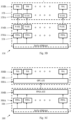
- FIGs. 3B and 3C depict schematic block diagrams of two optional architectures embodying MSU 310 of Fig. 3A , according to embodiments of the present invention.
- Fig. 3B depicts MSU 350 comprises FIU 356 and GPU 358.
- FIU 356 may comprise plurality of FIFO units (collectively named 356A) - FIFO 0 , FIFO 1 ... FIFO n . each FIFO unit may be in active communication with an assigned FPGA AXI (F-AXI) unit - F-AXI 0 , F-AXI 1 ... F-AXI n (collectively named 356B).
- F-AXI F-AXI
- Each of the separate F-AXI units may be in direct connection with an assigned GPU AXI (G-AXI) unit- G-AXI 0 , G-AXI 1 ... G-AXI n .each of the G-AXI interface units may be in active connection with, and may provide data to an assigned SM - SM 0 , SM 1 ... SM n .
- MSU 380 comprises FIU 386 and GPU 388.
- FIU 386 may comprise plurality of FIFO units (collectively named 386A) - FIFO 0 , FIFO 1 ... FIFO n .
- each FIFO unit may be in active communication with a FPGA AXI (F-AXI) unit that may be configured to control administer the data streams from the plurality of FIFO units into a single AXI stream.
- the AXI stream may be transmitted to an AXI interface unit 388A of GPU 388 and may then be divided to the respective SMs units - SM 0 , SM 1 ... SM n .
- the architecture depicted in Fig. 3B may provide a faster overall performance but may require larger number of pins (for an integrated circuit (IC) embodying the described circuit) and a larger number of wires/conduits.
- the architecture depicted in Fig. 3C may provide a relatively slower overall performance but may require smaller number of pins (for an integrated circuit (IC) embodying the described circuit) and a smaller number of wires/conduits.
Landscapes
- Engineering & Computer Science (AREA)
- Theoretical Computer Science (AREA)
- Software Systems (AREA)
- Physics & Mathematics (AREA)
- General Physics & Mathematics (AREA)
- General Engineering & Computer Science (AREA)
- Multimedia (AREA)
- Image Processing (AREA)
- Multi Processors (AREA)
- Memory System Of A Hierarchy Structure (AREA)
- Advance Control (AREA)
- Mathematical Physics (AREA)
- Computer Hardware Design (AREA)
Claims (7)
- Circuit pour la manipulation de données non traitées comprenant :
une unité de division de flux de données (DSDU) (304), comprenant :un réseau comprenant une pluralité de registres premier entré, premier sorti (FIFO), configuré pour recevoir un flux de données et pour le diviser en portions de données et pour acheminer chacune des portions de données à travers un de la pluralité de registres FIFO ; etune première interface extensible avancée (AXI) configurée pour recevoir les portions de données ; etune unité de traitement graphique (GPU) comprenant :une deuxième interface extensible avancée (AXI) configurée pour recevoir les portions de données de la première unité AXI ; etune pluralité de multiprocesseurs de flux (SM) configurés pour recevoir chaque portion de données d'un registre FIFO respectif et pour traiter la portion de données reçue. - Circuit selon la revendication 1, dans lequel un registre FIFO dans la DSDU est connecté à un SM affecté dans la GPU par le biais d'une première unité AXI affectée dans la DSDU et d'une deuxième unité AXI affectée dans la GPU.
- Circuit selon la revendication 1, dans lequel chacun des registres FIFO dans la DSDU est connecté à un SM affecté dans la GPU par le biais d'une première unité AXI commune dans la DSDU et d'une deuxième unité AXI commune dans la GPU.
- Procédé pour le traitement efficace d'un grand volume de données comprenant les étapes consistant à :recevoir, au niveau du diviseur de flux (DSDU) (304) défini dans la revendication 1, un flux de données non traitées ;diviser le flux en une pluralité de portions de données ;acheminer chaque portion de données par le biais d'un registre FIFO spécifique dans une unité de division de flux de données (DSDU) ; ettransférer la portion de données du registre FIFO spécifique à un multiprocesseur de flux affecté (SM) dans l'unité de traitement graphique (GPU) comme défini dans la revendication 1 pour traitement.
- Procédé selon la revendication 4, dans lequel les portions de données sont transférées par le biais d'une première unité d'interface extensible avancée (AXI) dans la DSDU et une deuxième unité d'interface extensible avancée (AXI) dans la GPU.
- Procédé selon la revendication 5, dans lequel une portion de données reçue d'un registre FIFO spécifique est transférée au SM affecté dans la GPU par le biais d'une première unité AXI affectée dans la DSDU et d'une deuxième unité AXI affectée dans la GPU.
- Procédé selon la revendication 5, dans lequel chacune des portions de données reçues des registres FIFO est transférée au SM affecté dans la GPU par le biais d'une première unité AXI commune dans la DSDU et d'une deuxième unité AXI commune dans la GPU.
Applications Claiming Priority (2)
| Application Number | Priority Date | Filing Date | Title |
|---|---|---|---|
| US201762552475P | 2017-08-31 | 2017-08-31 | |
| PCT/IL2018/050965 WO2019043710A1 (fr) | 2017-08-31 | 2018-08-30 | Système et procédé d'amélioration du débit dans de nombreux calculs |
Publications (4)
| Publication Number | Publication Date |
|---|---|
| EP3676710A1 EP3676710A1 (fr) | 2020-07-08 |
| EP3676710A4 EP3676710A4 (fr) | 2021-07-28 |
| EP3676710B1 true EP3676710B1 (fr) | 2025-05-14 |
| EP3676710C0 EP3676710C0 (fr) | 2025-05-14 |
Family
ID=65527276
Family Applications (1)
| Application Number | Title | Priority Date | Filing Date |
|---|---|---|---|
| EP18850323.9A Active EP3676710B1 (fr) | 2017-08-31 | 2018-08-30 | Système et procédé d'amélioration du débit dans de nombreux calculs |
Country Status (4)
| Country | Link |
|---|---|
| US (2) | US10942746B2 (fr) |
| EP (1) | EP3676710B1 (fr) |
| JP (2) | JP2020532795A (fr) |
| WO (1) | WO2019043710A1 (fr) |
Families Citing this family (2)
| Publication number | Priority date | Publication date | Assignee | Title |
|---|---|---|---|---|
| US11204819B2 (en) | 2018-12-21 | 2021-12-21 | Samsung Electronics Co., Ltd. | System and method for offloading application functions to a device |
| US20220147320A1 (en) * | 2020-11-09 | 2022-05-12 | Vizzio Technologies Pte Ltd | Highly parallel processing system |
Family Cites Families (22)
| Publication number | Priority date | Publication date | Assignee | Title |
|---|---|---|---|---|
| JPH0258153A (ja) * | 1988-08-24 | 1990-02-27 | Mitsubishi Electric Corp | 情報処理装置 |
| JPH06324997A (ja) * | 1993-05-10 | 1994-11-25 | Nippon Steel Corp | 複数のfifoメモリを内蔵したfifo記憶装置 |
| US6275536B1 (en) | 1999-06-23 | 2001-08-14 | General Instrument Corporation | Implementation architectures of a multi-channel MPEG video transcoder using multiple programmable processors |
| JP2001134490A (ja) * | 1999-11-01 | 2001-05-18 | Fujitsu Ltd | キャッシュメモリの制御方法及びその方法を実現する計算機 |
| JP4043225B2 (ja) * | 2001-12-10 | 2008-02-06 | 株式会社ルネサステクノロジ | キャッシュ装置および方法 |
| JP2006091982A (ja) | 2004-09-21 | 2006-04-06 | Canon Inc | オンチップバスシステム |
| EP1846834A2 (fr) | 2005-01-25 | 2007-10-24 | Lucid Information Technology, Ltd. | Systeme de traitement et d'affichage graphique utilisant plusieurs noyaux graphiques sur une puce en silicium de construction monolithique |
| JP4904802B2 (ja) * | 2005-02-01 | 2012-03-28 | セイコーエプソン株式会社 | キャッシュメモリ及びプロセッサ |
| JP4837305B2 (ja) * | 2005-05-10 | 2011-12-14 | ルネサスエレクトロニクス株式会社 | マイクロプロセッサ及びマイクロプロセッサの制御方法 |
| GB0723536D0 (en) * | 2007-11-30 | 2008-01-09 | Imagination Tech Ltd | Multi-core geometry processing in a tile based rendering system |
| US8400458B2 (en) * | 2009-09-09 | 2013-03-19 | Hewlett-Packard Development Company, L.P. | Method and system for blocking data on a GPU |
| US9639479B2 (en) * | 2009-09-23 | 2017-05-02 | Nvidia Corporation | Instructions for managing a parallel cache hierarchy |
| JP5487882B2 (ja) * | 2009-10-27 | 2014-05-14 | セイコーエプソン株式会社 | 画像処理装置および画像処理方法 |
| JP5648465B2 (ja) * | 2010-12-17 | 2015-01-07 | 富士通セミコンダクター株式会社 | グラフィックスプロセッサ |
| JP5659817B2 (ja) * | 2011-01-21 | 2015-01-28 | ソニー株式会社 | 相互接続装置 |
| US9092267B2 (en) * | 2011-06-20 | 2015-07-28 | Qualcomm Incorporated | Memory sharing in graphics processing unit |
| US8954599B2 (en) * | 2011-10-28 | 2015-02-10 | Hewlett-Packard Development Company, L.P. | Data stream operations |
| WO2013095640A1 (fr) | 2011-12-23 | 2013-06-27 | Intel Corporation | Procédés et appareil pour communication efficace entre caches dans une conception de mise en cache hiérarchique |
| WO2013101120A1 (fr) * | 2011-12-29 | 2013-07-04 | Intel Corporation | Algorithmes à base d'apprentissage en ligne permettant d'augmenter la rétention et la réutilisation de surfaces dynamiques générées par gpu dans des antémémoires de niveau extérieur |
| US9244683B2 (en) * | 2013-02-26 | 2016-01-26 | Nvidia Corporation | System, method, and computer program product for implementing large integer operations on a graphics processing unit |
| US9086813B2 (en) * | 2013-03-15 | 2015-07-21 | Qualcomm Incorporated | Method and apparatus to save and restore system memory management unit (MMU) contexts |
| US9489009B2 (en) | 2014-02-20 | 2016-11-08 | Samsung Electronics Co., Ltd. | System on chip, bus interface and method of operating the same |
-
2018
- 2018-08-30 WO PCT/IL2018/050965 patent/WO2019043710A1/fr not_active Ceased
- 2018-08-30 US US16/642,026 patent/US10942746B2/en active Active
- 2018-08-30 EP EP18850323.9A patent/EP3676710B1/fr active Active
- 2018-08-30 JP JP2020512508A patent/JP2020532795A/ja active Pending
-
2021
- 2021-02-03 US US17/167,077 patent/US20210191729A1/en not_active Abandoned
-
2023
- 2023-03-06 JP JP2023033382A patent/JP7547526B2/ja active Active
Also Published As
| Publication number | Publication date |
|---|---|
| EP3676710A1 (fr) | 2020-07-08 |
| US20200183698A1 (en) | 2020-06-11 |
| US20210191729A1 (en) | 2021-06-24 |
| US10942746B2 (en) | 2021-03-09 |
| EP3676710A4 (fr) | 2021-07-28 |
| JP2020532795A (ja) | 2020-11-12 |
| JP2023078204A (ja) | 2023-06-06 |
| EP3676710C0 (fr) | 2025-05-14 |
| JP7547526B2 (ja) | 2024-09-09 |
| WO2019043710A1 (fr) | 2019-03-07 |
Similar Documents
| Publication | Publication Date | Title |
|---|---|---|
| US12561057B2 (en) | Accelerated data processing in solid state drives (SSDs) with host processors and storage processing engines (SPEs) | |
| US12147849B2 (en) | Work stealing in heterogeneous computing systems | |
| US20200174977A1 (en) | Storage appliance for processing of functions as a service (faas) | |
| US10444813B2 (en) | Multi-criteria power management scheme for pooled accelerator architectures | |
| JP7547526B2 (ja) | 複数計算における高スループットのためのシステムおよび方法 | |
| US12417194B2 (en) | Programmable memory controller circuits and methods | |
| CN116402102A (zh) | 神经网络处理器和电子设备 | |
| CN113434813B (zh) | 一种基于神经网络的矩阵乘运算方法及相关装置 | |
| US7000041B2 (en) | Method and an apparatus to efficiently handle read completions that satisfy a read request | |
| US20060218332A1 (en) | Interface circuit, system, and method for interfacing between buses of different widths | |
| US12229078B2 (en) | Neural processing unit synchronization systems and methods | |
| EP4634787A1 (fr) | Génération de données fusionnées et communication associée | |
| EP2199919B1 (fr) | Méthod pour traiter des données en utilisant un triple tampon (triple buffering) | |
| US20180095929A1 (en) | Scratchpad memory with bank tiling for localized and random data access | |
| JP2006216060A (ja) | データ処理方法およびデータ処理システム | |
| US20200059437A1 (en) | Link layer data packing and packet flow control scheme | |
| US20240069965A1 (en) | Systems and methods for executing compute functions | |
| US20110022742A1 (en) | Processor and data transfer method | |
| US20080228958A1 (en) | Direct Memory Access Engine for Data Transfers | |
| EP4435600A1 (fr) | Systèmes et procédés d'exécution de fonctions de calcul | |
| US20230058749A1 (en) | Adaptive matrix multipliers | |
| CN121705215A (zh) | 请求处理方法及装置、电子设备和存储介质 |
Legal Events
| Date | Code | Title | Description |
|---|---|---|---|
| STAA | Information on the status of an ep patent application or granted ep patent |
Free format text: STATUS: THE INTERNATIONAL PUBLICATION HAS BEEN MADE |
|
| PUAI | Public reference made under article 153(3) epc to a published international application that has entered the european phase |
Free format text: ORIGINAL CODE: 0009012 |
|
| STAA | Information on the status of an ep patent application or granted ep patent |
Free format text: STATUS: REQUEST FOR EXAMINATION WAS MADE |
|
| 17P | Request for examination filed |
Effective date: 20200302 |
|
| AK | Designated contracting states |
Kind code of ref document: A1 Designated state(s): AL AT BE BG CH CY CZ DE DK EE ES FI FR GB GR HR HU IE IS IT LI LT LU LV MC MK MT NL NO PL PT RO RS SE SI SK SM TR |
|
| AX | Request for extension of the european patent |
Extension state: BA ME |
|
| DAV | Request for validation of the european patent (deleted) | ||
| DAX | Request for extension of the european patent (deleted) | ||
| RIC1 | Information provided on ipc code assigned before grant |
Ipc: G06T 1/60 20060101AFI20210309BHEP Ipc: G06F 12/08 20160101ALI20210309BHEP Ipc: G06F 12/0802 20160101ALI20210309BHEP Ipc: G06F 13/14 20060101ALI20210309BHEP Ipc: G06F 9/50 20060101ALI20210309BHEP Ipc: G06T 1/20 20060101ALI20210309BHEP |
|
| A4 | Supplementary search report drawn up and despatched |
Effective date: 20210624 |
|
| RIC1 | Information provided on ipc code assigned before grant |
Ipc: G06T 1/60 20060101AFI20210618BHEP Ipc: G06F 12/08 20160101ALI20210618BHEP Ipc: G06F 12/0802 20160101ALI20210618BHEP Ipc: G06F 13/14 20060101ALI20210618BHEP Ipc: G06F 9/50 20060101ALI20210618BHEP Ipc: G06T 1/20 20060101ALI20210618BHEP |
|
| REG | Reference to a national code |
Ref legal event code: R079 Free format text: PREVIOUS MAIN CLASS: G06F0012080000 Ref country code: DE Ref legal event code: R079 Ref document number: 602018081991 Country of ref document: DE Free format text: PREVIOUS MAIN CLASS: G06F0012080000 Ipc: G06T0001600000 |
|
| GRAP | Despatch of communication of intention to grant a patent |
Free format text: ORIGINAL CODE: EPIDOSNIGR1 |
|
| STAA | Information on the status of an ep patent application or granted ep patent |
Free format text: STATUS: GRANT OF PATENT IS INTENDED |
|
| RIC1 | Information provided on ipc code assigned before grant |
Ipc: G06T 1/60 20060101AFI20241127BHEP |
|
| INTG | Intention to grant announced |
Effective date: 20241217 |
|
| GRAS | Grant fee paid |
Free format text: ORIGINAL CODE: EPIDOSNIGR3 |
|
| GRAA | (expected) grant |
Free format text: ORIGINAL CODE: 0009210 |
|
| STAA | Information on the status of an ep patent application or granted ep patent |
Free format text: STATUS: THE PATENT HAS BEEN GRANTED |
|
| AK | Designated contracting states |
Kind code of ref document: B1 Designated state(s): AL AT BE BG CH CY CZ DE DK EE ES FI FR GB GR HR HU IE IS IT LI LT LU LV MC MK MT NL NO PL PT RO RS SE SI SK SM TR |
|
| REG | Reference to a national code |
Ref country code: GB Ref legal event code: FG4D |
|
| REG | Reference to a national code |
Ref country code: CH Ref legal event code: EP |
|
| REG | Reference to a national code |
Ref country code: DE Ref legal event code: R096 Ref document number: 602018081991 Country of ref document: DE |
|
| REG | Reference to a national code |
Ref country code: IE Ref legal event code: FG4D |
|
| U01 | Request for unitary effect filed |
Effective date: 20250610 |
|
| U07 | Unitary effect registered |
Designated state(s): AT BE BG DE DK EE FI FR IT LT LU LV MT NL PT RO SE SI Effective date: 20250618 |
|
| PG25 | Lapsed in a contracting state [announced via postgrant information from national office to epo] |
Ref country code: ES Free format text: LAPSE BECAUSE OF FAILURE TO SUBMIT A TRANSLATION OF THE DESCRIPTION OR TO PAY THE FEE WITHIN THE PRESCRIBED TIME-LIMIT Effective date: 20250514 |
|
| PG25 | Lapsed in a contracting state [announced via postgrant information from national office to epo] |
Ref country code: GR Free format text: LAPSE BECAUSE OF FAILURE TO SUBMIT A TRANSLATION OF THE DESCRIPTION OR TO PAY THE FEE WITHIN THE PRESCRIBED TIME-LIMIT Effective date: 20250815 Ref country code: NO Free format text: LAPSE BECAUSE OF FAILURE TO SUBMIT A TRANSLATION OF THE DESCRIPTION OR TO PAY THE FEE WITHIN THE PRESCRIBED TIME-LIMIT Effective date: 20250814 |
|
| PG25 | Lapsed in a contracting state [announced via postgrant information from national office to epo] |
Ref country code: PL Free format text: LAPSE BECAUSE OF FAILURE TO SUBMIT A TRANSLATION OF THE DESCRIPTION OR TO PAY THE FEE WITHIN THE PRESCRIBED TIME-LIMIT Effective date: 20250514 |
|
| PG25 | Lapsed in a contracting state [announced via postgrant information from national office to epo] |
Ref country code: HR Free format text: LAPSE BECAUSE OF FAILURE TO SUBMIT A TRANSLATION OF THE DESCRIPTION OR TO PAY THE FEE WITHIN THE PRESCRIBED TIME-LIMIT Effective date: 20250514 |
|
| PG25 | Lapsed in a contracting state [announced via postgrant information from national office to epo] |
Ref country code: RS Free format text: LAPSE BECAUSE OF FAILURE TO SUBMIT A TRANSLATION OF THE DESCRIPTION OR TO PAY THE FEE WITHIN THE PRESCRIBED TIME-LIMIT Effective date: 20250814 |
|
| PG25 | Lapsed in a contracting state [announced via postgrant information from national office to epo] |
Ref country code: IS Free format text: LAPSE BECAUSE OF FAILURE TO SUBMIT A TRANSLATION OF THE DESCRIPTION OR TO PAY THE FEE WITHIN THE PRESCRIBED TIME-LIMIT Effective date: 20250914 |
|
| REG | Reference to a national code |
Ref country code: CH Ref legal event code: U11 Free format text: ST27 STATUS EVENT CODE: U-0-0-U10-U11 (AS PROVIDED BY THE NATIONAL OFFICE) Effective date: 20251115 |
|
| U21 | Renewal fee for the european patent with unitary effect paid with additional fee |
Year of fee payment: 8 Effective date: 20251118 |
|
| PGFP | Annual fee paid to national office [announced via postgrant information from national office to epo] |
Ref country code: GB Payment date: 20251114 Year of fee payment: 8 |
|
| PG25 | Lapsed in a contracting state [announced via postgrant information from national office to epo] |
Ref country code: SM Free format text: LAPSE BECAUSE OF FAILURE TO SUBMIT A TRANSLATION OF THE DESCRIPTION OR TO PAY THE FEE WITHIN THE PRESCRIBED TIME-LIMIT Effective date: 20250514 |
|
| PGFP | Annual fee paid to national office [announced via postgrant information from national office to epo] |
Ref country code: CH Payment date: 20251115 Year of fee payment: 8 |
|
| PG25 | Lapsed in a contracting state [announced via postgrant information from national office to epo] |
Ref country code: CZ Free format text: LAPSE BECAUSE OF FAILURE TO SUBMIT A TRANSLATION OF THE DESCRIPTION OR TO PAY THE FEE WITHIN THE PRESCRIBED TIME-LIMIT Effective date: 20250514 |
|
| PG25 | Lapsed in a contracting state [announced via postgrant information from national office to epo] |
Ref country code: SK Free format text: LAPSE BECAUSE OF FAILURE TO SUBMIT A TRANSLATION OF THE DESCRIPTION OR TO PAY THE FEE WITHIN THE PRESCRIBED TIME-LIMIT Effective date: 20250514 |
|
| PLBE | No opposition filed within time limit |
Free format text: ORIGINAL CODE: 0009261 |
|
| STAA | Information on the status of an ep patent application or granted ep patent |
Free format text: STATUS: NO OPPOSITION FILED WITHIN TIME LIMIT |
|
| REG | Reference to a national code |
Ref country code: CH Ref legal event code: L10 Free format text: ST27 STATUS EVENT CODE: U-0-0-L10-L00 (AS PROVIDED BY THE NATIONAL OFFICE) Effective date: 20260325 |
|
| PG25 | Lapsed in a contracting state [announced via postgrant information from national office to epo] |
Ref country code: MC Free format text: LAPSE BECAUSE OF FAILURE TO SUBMIT A TRANSLATION OF THE DESCRIPTION OR TO PAY THE FEE WITHIN THE PRESCRIBED TIME-LIMIT Effective date: 20250514 |
|
| 26N | No opposition filed |
Effective date: 20260217 |