EP3677958B1 - Empilement et dispositif d'affichage à cristaux liquides comprenant ce dernier - Google Patents
Empilement et dispositif d'affichage à cristaux liquides comprenant ce dernier Download PDFInfo
- Publication number
- EP3677958B1 EP3677958B1 EP19815371.0A EP19815371A EP3677958B1 EP 3677958 B1 EP3677958 B1 EP 3677958B1 EP 19815371 A EP19815371 A EP 19815371A EP 3677958 B1 EP3677958 B1 EP 3677958B1
- Authority
- EP
- European Patent Office
- Prior art keywords
- wave plate
- plate
- liquid crystal
- quarter wave
- positive
- Prior art date
- Legal status (The legal status is an assumption and is not a legal conclusion. Google has not performed a legal analysis and makes no representation as to the accuracy of the status listed.)
- Active
Links
Images

Classifications
-
- G—PHYSICS
- G02—OPTICS
- G02F—OPTICAL DEVICES OR ARRANGEMENTS FOR THE CONTROL OF LIGHT BY MODIFICATION OF THE OPTICAL PROPERTIES OF THE MEDIA OF THE ELEMENTS INVOLVED THEREIN; NON-LINEAR OPTICS; FREQUENCY-CHANGING OF LIGHT; OPTICAL LOGIC ELEMENTS; OPTICAL ANALOGUE/DIGITAL CONVERTERS
- G02F1/00—Devices or arrangements for the control of the intensity, colour, phase, polarisation or direction of light arriving from an independent light source, e.g. switching, gating or modulating; Non-linear optics
- G02F1/01—Devices or arrangements for the control of the intensity, colour, phase, polarisation or direction of light arriving from an independent light source, e.g. switching, gating or modulating; Non-linear optics for the control of the intensity, phase, polarisation or colour
- G02F1/13—Devices or arrangements for the control of the intensity, colour, phase, polarisation or direction of light arriving from an independent light source, e.g. switching, gating or modulating; Non-linear optics for the control of the intensity, phase, polarisation or colour based on liquid crystals, e.g. single liquid crystal display cells
- G02F1/133—Constructional arrangements; Operation of liquid crystal cells; Circuit arrangements
- G02F1/1333—Constructional arrangements; Manufacturing methods
- G02F1/1335—Structural association of cells with optical devices, e.g. polarisers or reflectors
- G02F1/13363—Birefringent elements, e.g. for optical compensation
-
- B—PERFORMING OPERATIONS; TRANSPORTING
- B32—LAYERED PRODUCTS
- B32B—LAYERED PRODUCTS, i.e. PRODUCTS BUILT-UP OF STRATA OF FLAT OR NON-FLAT, e.g. CELLULAR OR HONEYCOMB, FORM
- B32B27/00—Layered products comprising a layer of synthetic resin
- B32B27/30—Layered products comprising a layer of synthetic resin comprising vinyl (co)polymers; comprising acrylic (co)polymers
-
- G—PHYSICS
- G02—OPTICS
- G02B—OPTICAL ELEMENTS, SYSTEMS OR APPARATUS
- G02B5/00—Optical elements other than lenses
- G02B5/30—Polarising elements
-
- G—PHYSICS
- G02—OPTICS
- G02B—OPTICAL ELEMENTS, SYSTEMS OR APPARATUS
- G02B5/00—Optical elements other than lenses
- G02B5/30—Polarising elements
- G02B5/3025—Polarisers, i.e. arrangements capable of producing a definite output polarisation state from an unpolarised input state
- G02B5/3033—Polarisers, i.e. arrangements capable of producing a definite output polarisation state from an unpolarised input state in the form of a thin sheet or foil, e.g. Polaroid
- G02B5/3041—Polarisers, i.e. arrangements capable of producing a definite output polarisation state from an unpolarised input state in the form of a thin sheet or foil, e.g. Polaroid comprising multiple thin layers, e.g. multilayer stacks
- G02B5/305—Polarisers, i.e. arrangements capable of producing a definite output polarisation state from an unpolarised input state in the form of a thin sheet or foil, e.g. Polaroid comprising multiple thin layers, e.g. multilayer stacks including organic materials, e.g. polymeric layers
-
- G—PHYSICS
- G02—OPTICS
- G02F—OPTICAL DEVICES OR ARRANGEMENTS FOR THE CONTROL OF LIGHT BY MODIFICATION OF THE OPTICAL PROPERTIES OF THE MEDIA OF THE ELEMENTS INVOLVED THEREIN; NON-LINEAR OPTICS; FREQUENCY-CHANGING OF LIGHT; OPTICAL LOGIC ELEMENTS; OPTICAL ANALOGUE/DIGITAL CONVERTERS
- G02F1/00—Devices or arrangements for the control of the intensity, colour, phase, polarisation or direction of light arriving from an independent light source, e.g. switching, gating or modulating; Non-linear optics
- G02F1/01—Devices or arrangements for the control of the intensity, colour, phase, polarisation or direction of light arriving from an independent light source, e.g. switching, gating or modulating; Non-linear optics for the control of the intensity, phase, polarisation or colour
- G02F1/13—Devices or arrangements for the control of the intensity, colour, phase, polarisation or direction of light arriving from an independent light source, e.g. switching, gating or modulating; Non-linear optics for the control of the intensity, phase, polarisation or colour based on liquid crystals, e.g. single liquid crystal display cells
- G02F1/133—Constructional arrangements; Operation of liquid crystal cells; Circuit arrangements
- G02F1/1333—Constructional arrangements; Manufacturing methods
- G02F1/1335—Structural association of cells with optical devices, e.g. polarisers or reflectors
-
- G—PHYSICS
- G02—OPTICS
- G02F—OPTICAL DEVICES OR ARRANGEMENTS FOR THE CONTROL OF LIGHT BY MODIFICATION OF THE OPTICAL PROPERTIES OF THE MEDIA OF THE ELEMENTS INVOLVED THEREIN; NON-LINEAR OPTICS; FREQUENCY-CHANGING OF LIGHT; OPTICAL LOGIC ELEMENTS; OPTICAL ANALOGUE/DIGITAL CONVERTERS
- G02F1/00—Devices or arrangements for the control of the intensity, colour, phase, polarisation or direction of light arriving from an independent light source, e.g. switching, gating or modulating; Non-linear optics
- G02F1/01—Devices or arrangements for the control of the intensity, colour, phase, polarisation or direction of light arriving from an independent light source, e.g. switching, gating or modulating; Non-linear optics for the control of the intensity, phase, polarisation or colour
- G02F1/13—Devices or arrangements for the control of the intensity, colour, phase, polarisation or direction of light arriving from an independent light source, e.g. switching, gating or modulating; Non-linear optics for the control of the intensity, phase, polarisation or colour based on liquid crystals, e.g. single liquid crystal display cells
- G02F1/133—Constructional arrangements; Operation of liquid crystal cells; Circuit arrangements
- G02F1/1333—Constructional arrangements; Manufacturing methods
- G02F1/1335—Structural association of cells with optical devices, e.g. polarisers or reflectors
- G02F1/133528—Polarisers
-
- G—PHYSICS
- G02—OPTICS
- G02F—OPTICAL DEVICES OR ARRANGEMENTS FOR THE CONTROL OF LIGHT BY MODIFICATION OF THE OPTICAL PROPERTIES OF THE MEDIA OF THE ELEMENTS INVOLVED THEREIN; NON-LINEAR OPTICS; FREQUENCY-CHANGING OF LIGHT; OPTICAL LOGIC ELEMENTS; OPTICAL ANALOGUE/DIGITAL CONVERTERS
- G02F1/00—Devices or arrangements for the control of the intensity, colour, phase, polarisation or direction of light arriving from an independent light source, e.g. switching, gating or modulating; Non-linear optics
- G02F1/01—Devices or arrangements for the control of the intensity, colour, phase, polarisation or direction of light arriving from an independent light source, e.g. switching, gating or modulating; Non-linear optics for the control of the intensity, phase, polarisation or colour
- G02F1/13—Devices or arrangements for the control of the intensity, colour, phase, polarisation or direction of light arriving from an independent light source, e.g. switching, gating or modulating; Non-linear optics for the control of the intensity, phase, polarisation or colour based on liquid crystals, e.g. single liquid crystal display cells
- G02F1/133—Constructional arrangements; Operation of liquid crystal cells; Circuit arrangements
- G02F1/1333—Constructional arrangements; Manufacturing methods
- G02F1/1335—Structural association of cells with optical devices, e.g. polarisers or reflectors
- G02F1/133528—Polarisers
- G02F1/133531—Polarisers characterised by the arrangement of polariser or analyser axes
-
- G—PHYSICS
- G02—OPTICS
- G02F—OPTICAL DEVICES OR ARRANGEMENTS FOR THE CONTROL OF LIGHT BY MODIFICATION OF THE OPTICAL PROPERTIES OF THE MEDIA OF THE ELEMENTS INVOLVED THEREIN; NON-LINEAR OPTICS; FREQUENCY-CHANGING OF LIGHT; OPTICAL LOGIC ELEMENTS; OPTICAL ANALOGUE/DIGITAL CONVERTERS
- G02F1/00—Devices or arrangements for the control of the intensity, colour, phase, polarisation or direction of light arriving from an independent light source, e.g. switching, gating or modulating; Non-linear optics
- G02F1/01—Devices or arrangements for the control of the intensity, colour, phase, polarisation or direction of light arriving from an independent light source, e.g. switching, gating or modulating; Non-linear optics for the control of the intensity, phase, polarisation or colour
- G02F1/13—Devices or arrangements for the control of the intensity, colour, phase, polarisation or direction of light arriving from an independent light source, e.g. switching, gating or modulating; Non-linear optics for the control of the intensity, phase, polarisation or colour based on liquid crystals, e.g. single liquid crystal display cells
- G02F1/133—Constructional arrangements; Operation of liquid crystal cells; Circuit arrangements
- G02F1/1333—Constructional arrangements; Manufacturing methods
- G02F1/1337—Surface-induced orientation of the liquid crystal molecules, e.g. by alignment layers
-
- G—PHYSICS
- G02—OPTICS
- G02F—OPTICAL DEVICES OR ARRANGEMENTS FOR THE CONTROL OF LIGHT BY MODIFICATION OF THE OPTICAL PROPERTIES OF THE MEDIA OF THE ELEMENTS INVOLVED THEREIN; NON-LINEAR OPTICS; FREQUENCY-CHANGING OF LIGHT; OPTICAL LOGIC ELEMENTS; OPTICAL ANALOGUE/DIGITAL CONVERTERS
- G02F1/00—Devices or arrangements for the control of the intensity, colour, phase, polarisation or direction of light arriving from an independent light source, e.g. switching, gating or modulating; Non-linear optics
- G02F1/01—Devices or arrangements for the control of the intensity, colour, phase, polarisation or direction of light arriving from an independent light source, e.g. switching, gating or modulating; Non-linear optics for the control of the intensity, phase, polarisation or colour
- G02F1/13—Devices or arrangements for the control of the intensity, colour, phase, polarisation or direction of light arriving from an independent light source, e.g. switching, gating or modulating; Non-linear optics for the control of the intensity, phase, polarisation or colour based on liquid crystals, e.g. single liquid crystal display cells
- G02F1/133—Constructional arrangements; Operation of liquid crystal cells; Circuit arrangements
- G02F1/1333—Constructional arrangements; Manufacturing methods
- G02F1/1335—Structural association of cells with optical devices, e.g. polarisers or reflectors
- G02F1/13363—Birefringent elements, e.g. for optical compensation
- G02F1/133634—Birefringent elements, e.g. for optical compensation the refractive index Nz perpendicular to the element surface being different from in-plane refractive indices Nx and Ny, e.g. biaxial or with normal optical axis
-
- G—PHYSICS
- G02—OPTICS
- G02F—OPTICAL DEVICES OR ARRANGEMENTS FOR THE CONTROL OF LIGHT BY MODIFICATION OF THE OPTICAL PROPERTIES OF THE MEDIA OF THE ELEMENTS INVOLVED THEREIN; NON-LINEAR OPTICS; FREQUENCY-CHANGING OF LIGHT; OPTICAL LOGIC ELEMENTS; OPTICAL ANALOGUE/DIGITAL CONVERTERS
- G02F1/00—Devices or arrangements for the control of the intensity, colour, phase, polarisation or direction of light arriving from an independent light source, e.g. switching, gating or modulating; Non-linear optics
- G02F1/01—Devices or arrangements for the control of the intensity, colour, phase, polarisation or direction of light arriving from an independent light source, e.g. switching, gating or modulating; Non-linear optics for the control of the intensity, phase, polarisation or colour
- G02F1/13—Devices or arrangements for the control of the intensity, colour, phase, polarisation or direction of light arriving from an independent light source, e.g. switching, gating or modulating; Non-linear optics for the control of the intensity, phase, polarisation or colour based on liquid crystals, e.g. single liquid crystal display cells
- G02F1/133—Constructional arrangements; Operation of liquid crystal cells; Circuit arrangements
- G02F1/1333—Constructional arrangements; Manufacturing methods
- G02F1/1335—Structural association of cells with optical devices, e.g. polarisers or reflectors
- G02F1/13363—Birefringent elements, e.g. for optical compensation
- G02F1/133638—Waveplates, i.e. plates with a retardation value of lambda/n
Definitions
- This application relates to a laminate and a liquid crystal display comprising the same.
- a lightweight thin film flat panel display which replaces a cathode ray tube (CRT) which is the existing display device
- FPD lightweight thin film flat panel display
- CRT cathode ray tube
- a liquid crystal display as a device for displaying an image using optical anisotropy of a liquid crystal is excellent in resolution, color display, and image quality and is actively applied to a notebook or a desktop monitor.
- liquid crystal molecules of a liquid crystal layer are driven by a difference in voltage applied to a common electrode and a pixel electrode.
- Liquid crystals have features such as dielectric anisotropy and refractive anisotropy.
- the dielectric anisotropy means that the degree of polarization induced by an electric field varies depending on long axis and short axis directions of the liquid crystal and the refractive anisotropy means that a refractive index varies depending on the long axis and short axis directions of the liquid crystal, which causes a polarization state to be changed because the refractive index felt varies according to a direction when light passes through the liquid crystal molecules.
- the liquid crystal display has a liquid crystal panel constituted by a pair of transparent insulating substrates formed by planes facing each other with the liquid crystal layer interposed therebetween as a required component and arbitrarily controls the polarization of the liquid crystal molecules through a change in electric field between respective electric field generating electrodes and displays various images by using transmittance of light which is changed at this time.
- a polarizer is located at each of upper and lower portions of the liquid crystal panel and the polarizer transmits the light of a polarization component, which coincides with a transmission axis to determine a transmission degree of light by arrangement of transmission axes of two polarizers and arrangement characteristics of the liquid crystals.
- the polarizer used in the liquid crystal display in the related art is mainly a PVA elongated type in which iodine ions are aligned through stretching by using polyvinyl alcohol (PVA) having good adsorption ability with iodine.
- PVA polyvinyl alcohol
- US 2010 149 459 describes a liquid crystal display device including a liquid crystal panel, and a view angle control film that controls a view angle of the liquid crystal panel.
- the view angle control film is a laminated film including at least a liquid crystal film and a linearly polarizing plate.
- liquid crystal molecules are solidified while being aligned with major axes tilted in a predetermined azimuth angle direction from a normal direction of a film surface.
- the linearly polarizing plate of the view angle control film and the linearly polarizing plate of the liquid crystal panel are placed so that polarization transmission axes thereof cross a major axis direction of the liquid crystal molecules when seen from the normal direction.
- US 2013 050 618 discloses a VA mode liquid crystal display with parallel polarizers.
- This application has been made in an effort to provide a liquid crystal display capable of resolving a size limitation of a polarizer and having an enhanced front CR characteristic.
- An embodiment of this application provides a laminate, as defined in appended claim 1, which comprises: a first polarization rotation layer; a second polarization rotation layer; and a positive C plate provided between the first polarization rotation layer and the second polarization rotation layer, the first polarization rotation layer comprises a first half wave plate and a first quarter wave plate, and the second polarization rotation layer comprises a second half wave plate and a second quarter wave plate.
- a liquid crystal display as defined in appended claim 4, which comprises: an upper polarizer; a lower polarizer; and a liquid crystal panel provided between the upper polarizer and the lower polarizer, the upper polarizer and the lower polarizer are provided so that absorption axes are parallel to each other, the liquid crystal display sequentially comprises the first polarization rotation layer, the positive C plate, and the second polarization rotation layer between the upper polarizer and the liquid crystal panel, the first polarization rotation layer comprises the first half wave plate and the first quarter wave plate, the second polarization rotation layer comprises the second half wave plate and the second quarter wave plate, and the liquid crystal panel is a vertical alignment liquid crystal mode.
- absorption axes of an upper polarizer and a lower polarizer of a liquid crystal display are provided to be parallel to each other, thereby resolving a size limitation of a polarizer according to a width of a polarizer raw material.
- a first polarization rotation layer, a positive C plate, and a second polarization rotation layer are comprised between an upper polarizer and a liquid crystal panel, and as a result, black luminance is reduced due to scattering of side light to increase a front contrast ratio (CR) as compared with a case where the first polarization rotation layer, the positive C plate, and the second polarization rotation layer are provided between a lower polarizer and the liquid crystal panel.
- CR front contrast ratio
- the positive C plate is comprised between the first polarization rotation layer and the second polarization rotation layer to minimize reduction of a contrast ratio (CR) at a viewing angle.
- CR contrast ratio
- an absorption axis of any one polarizer of an upper polarizer and a lower polarizer is set to 0 degree and the absorption axis of the other one polarizer is set to 90 degrees and the absorption axes of the upper polarizer and the lower polarizer are orthogonal to each other.
- a horizontal length of the polarizer is limited by a width of a roll that manufactures the polarizer, which becomes a limiting factor for enlarging a product size.
- a maximum width of the roll that manufactures a current polarizer is approximately 2600 mm, which means that a maximum size of a 21:9 standard TV is approximately a 110 inch level.
- a method for transversely stretching a polyvinyl alcohol (PVA) film to form the absorption axis of a polarizer roll in the TD is proposed.
- PVA polyvinyl alcohol
- the absorption axes of the upper polarizer and the lower polarizer of the liquid crystal display are all set to 0 degree, thereby resolving the size limitation of the polarizer according to the width of the polarizer raw material.
- a laminate according to an embodiment of this application, as defined in appended claim 1, comprises: a first polarization rotation layer; a second polarization rotation layer; and a positive C plate provided between the first polarization rotation layer and the second polarization rotation layer, the first polarization rotation layer comprises a first half wave plate and a first quarter wave plate, and the second polarization rotation layer comprises a second half wave plate and a second quarter wave plate.
- a liquid crystal display comprises: an upper polarizer; a lower polarizer; and a liquid crystal panel provided between the upper polarizer and the lower polarizer, the upper polarizer and the lower polarizer are provided so that absorption axes are parallel to each other, the liquid crystal display sequentially comprises the first polarization rotation layer, the positive C plate, and the second polarization rotation layer between the upper polarizer and the liquid crystal panel, the first polarization rotation layer comprises the first half wave plate and the first quarter wave plate, the second polarization rotation layer comprises the second half wave plate and the second quarter wave plate, and the liquid crystal panel is a vertical alignment liquid crystal mode.
- the upper polarizer and the lower polarizer are provided such that the absorption axes thereof are parallel to each other.
- both of the absorption axes of the upper polarizer and the lower polarizer may be 0 degree in order to resolve the size limitation of the polarizer according to a width of a polarizer raw material.
- the case where the liquid crystal display comprises the first polarization rotation layer, the positive C plate, and the second polarization rotation layer between the upper polarizer and the liquid crystal panel is more preferable than the case (not according to the claims) where the liquid crystal display comprises the first polarization rotation layer, the positive C plate, and the second polarization rotation layer between the lower polarizer and the liquid crystal panel.
- the polarizer attached to a TFT glass surface, which is a lower portion of the liquid crystal panel, based on the liquid crystal panel is referred to as the lower polarizer and the polarizer attached to an upper portion of the liquid crystal panel which is the opposite side thereof is referred to as the upper polarizer.
- Light emitted from a backlight unit (BLU) and incident on the lower polarizer has a black luminance rising element at the front due to scattering inside a cell in a lower panel.
- scattered light may be absorbed by the polarizer of an upper plate as long as there is no retardation of a lower plate, so that as compared with the case (which is not according to the claims) where the liquid crystal display comprises the first polarization rotation layer, the positive C plate, and the second polarization rotation layer between the lower polarizer and the liquid crystal panel, in the case (according to the claims) where the liquid crystal display comprises the first polarization rotation layer, the positive C plate, and the second polarization rotation layer between the upper polarizer and the liquid crystal panel, the black luminance is reduced due to side light scattering, and as a result, a front CR is raised.
- the first quarter wave plate of the first polarization rotation layer is provided on the positive C plate and the second quarter wave plate of the second polarization rotation layer is provided on the positive C plate.
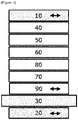
- the laminate according to an embodiment of this application is a lamination structure of the first half wave plate/the first quarter wave plate/the positive C plate/the second quarter wave plate/the second half wave plate.
- the liquid crystal display according to an embodiment of this application is a lamination structure of the upper polarizer/the first half wave plate/the first quarter wave plate/the positive C plate/the second quarter wave plate/the second half wave plate/the liquid crystal panel/the lower polarizer.
- an angle formed between an optical axis of the first half wave plate of the first polarization rotation layer and the absorption axis of the upper polarizer may be 10 to 20 degrees and may be 12.5 to 17.5 degrees and the angle between the optical axis of the first quarter wave plate of the first polarization rotation layer and the absorption axis of the upper polarizer may be 70 to 80 degrees and may be 72.5 to 77.5 degrees.
- the angle formed between the optical axis of the second quarter wave plate of the second polarization rotation layer and the absorption axis of the upper polarizer may be 10 to 20 degrees and may be 12.5 to 17.5 degrees and the angle formed between the optical axis of the second half wave plate of the second polarization rotation layer and the absorption axis of the upper polarizer may be 70 to 80 degrees and may be 72.5 to 77.5 degrees.
- the optical axis is not orthogonal to the absorption axis of the upper polarizer and light leakage occurs in black and the C/R thus drops.
- the angle formed between the optical axis of the first half wave plate of the first polarization rotation layer and the absorption axis of the upper polarizer is 15 degrees and the angle formed between the optical axis of the first quarter wave plate and the absorption axis of the upper polarizer is 75 degrees.
- the angle formed between the optical axis of the second quarter wave plate of the second polarization rotation layer and the absorption axis of the upper polarizer is 15 degrees and the angle formed between the optical axis of the first half wave plate and the absorption axis of the upper polarizer is 75 degrees.
- the reason for setting the above range is that consideration is given to manufacturing tolerances of general optical films.
- the first half wave plate and the second half wave plate may be made of materials known in the art and are not particularly limited.
- polyolefin polyethylene, polypropylene, polynorbornene and the like
- amorphous polyolefin polyimide, polyamideimide, polyamide, polyetherimide, polyetheretherketone, polyetherketone, polyketone sulfide, polyether sulfone, polysulfone, polyphenylene sulfide, polyphenylene oxide, polyethylene terephthalate, polybutylene terephthalate, polyethylene naphthalate, polyacetal, polycarbonate, polyarylate, polymethyl methacrylate, polymethacrylate, polyacrylate, polystyrene, cellulose-based polymer (such as triacetyl cellulose), PVA, epoxy resin, phenol resin, norbornene resin, polyester resin, acrylic resin, vinyl chloride resin, vinylidene chloride resin, etc., may be singly used or two
- the first half wave plate and the second half wave plate may be obtained by forming the resin compositions and performing uniaxial or biaxial stretching. Further, as the first half wave plate and the second half wave plate, an alignment film in which a liquid crystalline polymer or a liquid crystalline monomer is aligned may be used.
- the first half wave plate and the second half wave plate are retarders in which the retardation is implemented as half so that the relative phase difference between the e-ray and the o-ray becomes ⁇ .
- the phase difference may be represented as ⁇ nd and the half wave plate may be manufactured by adjusting a thickness according to ⁇ nd of a material.
- the first quarter wave plate and the second quarter wave plate may be made of materials known in the art and is not particularly limited.
- the quarter wave plate may be formed by a uniaxially stretched cycloolefin film, a uniaxially stretched polyethylene terephthalate film, a uniaxially stretched polycarbonate film, or a liquid crystal film.
- the first quarter wave plate and the second quarter wave plate may be obtained by forming the resin compositions and performing uniaxial or biaxial stretching. Further, as the first quarter wave plate and the second quarter wave plate, an alignment film in which a liquid crystalline polymer or a liquid crystalline monomer is aligned may be used.
- the first quarter wave plate and the second quarter wave plate are films made so that the relative phase difference between the e-ray and the o-ray becomes ⁇ /2.
- Linear polarization is made to be circular polarization or the circular polarization is made to be the linear polarization.
- the positive C plate is provided between the first polarization rotation layer and the second polarization rotation layer.
- n x represents a refractive index in a direction in which a plane-direction refractive index of the film becomes maximum
- n y represents a refractive index in a vertical direction in respects to an n x direction in a plane direction of the film
- n z represents a thickness-direction refractive index of the film.
- the positive C plate may be known to the art and is not particularly limited. More specifically, the positive C plate may be prepared by aligning a polymer film in an appropriate method or may be prepared by coating a polymeric cholesteric liquid crystal compound on one surface of a substrate, aligning the polymer film in a predetermined direction, and then curing. When the polymerizable cholesteric liquid crystal compound is used, a zero retardation film may be used as the substrate. In this application, the zero retardation film means a film in which substantially no retardation does not occur even though light is transmitted.
- the generally used positive C plate as a vertical alignment liquid crystal layer may mean a liquid crystal polymer layer comprising substantially vertically aligned liquid crystals and the polymer layer may represent so-called characteristics of the positive C plate.
- the characteristic of the positive C plate means that the refractive index n x in a slow axis direction is substantially equal to the refractive index n y in the fast axis direction and the refractive index n z in a thickness direction is larger than the refractive index n x in the slow axis direction (n z > n x ).
- the refractive index n x in the slow axis direction is substantially equal to the refractive index n y in the fast axis direction, and as a result, a case where there is a minute difference which occurs due to a process error, etc., is comprised in a scope of substantial equaling.
- the vertical alignment liquid crystal layer may comprise some liquid crystals which are not vertically aligned if the vertical alignment liquid crystal layer shows the characteristics of the positive C plate.
- a dispersion characteristic may have a positive dispersion characteristic or a negative dispersion characteristic.
- a thickness-direction retardation value R th of the positive C plate which is represented by Equation 1 below in 550 nm is in the range of 50 to 200 nm. Further, a front retardation value R o of the positive C plate, which is represented by Equation 2 below in 550 nm is in the range of -5 to 5 nm or may be 0.
- R th n z ⁇ n x + n y / 2 ⁇ d
- R o n x ⁇ n y ⁇ d
- n x represents a refractive index in a direction in which the plane-direction refractive index of the positive C plate becomes maximum
- n y represents the refractive index in the vertical direction in respects to the n x direction in the plane direction of the positive C plate
- n z represents the thickness-direction refractive index of the positive C plate
- d represents a thickness of the positive C plate.
- a first viewing angle compensation film may be additionally comprised between the second polarization rotation layer and the liquid crystal panel and the first viewing angle compensation film may comprise a negative B plate.
- the negative B plate means a film having a refractive index distribution of n x > n y > n z .
- n x represents a refractive index in a direction in which a plane-direction refractive index of the film becomes maximum
- n y represents a refractive index in a vertical direction in respects to an n x direction in a plane direction of the film
- n z represents a thickness-direction refractive index of the film.
- the thickness-direction retardation value R th of the negative B plate which is represented by Equation 3 below in 550 nm may be in the range of -230 to -330 nm.
- the front retardation value R o of the negative B plate which is represented by Equation 4 below in 550 nm may be in the range of 10 to 110 nm.
- R th n z ⁇ n x + n y / 2 ⁇ d
- R o n x ⁇ n y ⁇ d
- n x represents a refractive index in a direction in which the plane-direction refractive index of the negative B plate becomes the maximum
- n y represents the refractive index in the vertical direction in respects to the n x direction in the plane direction of the negative B plate
- n z represents the thickness-direction refractive index of the negative B plate
- d represents a thickness of the negative B plate.
- a second viewing angle compensation film may be additionally comprised between the liquid crystal panel and the lower polarizer and the second viewing angle compensation film may comprise a positive A plate and a negative C plate.
- n x represents a refractive index in a direction in which a plane-direction refractive index of the film becomes maximum
- n y represents a refractive index in the vertical direction in respects to an n x direction in a plane direction of the film
- n z represents a thickness-direction refractive index of the film.
- the front retardation value R o of the positive A plate which is represented by Equation 5 below in 550 nm may be in the range of 90 to 190 nm.
- R o n x ⁇ n y ⁇ d
- n x represents a refractive index in a direction in which the plane-direction refractive index of the positive A plate becomes the maximum
- n y represents the refractive index in the vertical direction in respects to the n x direction in the plane direction of the positive A plate
- d represents a thickness of the positive A plate.
- the C/R may drop due to the light leakage in a black state because retardation compensation of the vertically aligned liquid crystals is not completely made at a viewing angle.
- the thickness-direction retardation value R th of the negative C plate which is represented by Equation 6 below in 550 nm may be in the range of -160 to -260 nm.
- the front retardation value R o of the positive C plate which is represented by Equation 7 below in 550 nm may be in the range of -5 to 5 nm or may be 0.
- R th n z ⁇ n x + n y / 2 ⁇ d
- R o n x ⁇ n y ⁇ d
- n x represents a refractive index in a direction in which the plane-direction refractive index of the negative C plate becomes maximum
- n y represents the refractive index in the vertical direction in respects to the n x direction in the plane direction of the negative C plate
- n z represents the thickness-direction refractive index of the negative C plate
- d represents a thickness of the negative C plate.
- wave dispersibilities of the first half wave plate, the second ⁇ / wave plate, the first quarter wave plate, and the second quarter wave plate may be independently constant dispersibility or flat dispersibility.
- each of wave dispersibilities of the first half wave plate, the second ⁇ / wave plate, the first quarter wave plate, and the second quarter wave plate is the constant dispersibility
- front C/R characteristics may be more excellent as compared with the case where each wave dispersbility is the flat dispersibility.
- the constant dispersibility means a characteristic that as a wavelength of incident light increases, the generated retardation value decreases and the flat dispersibility means a characteristic that a retardation value of a similar degree is generated regardless of the wavelength of the incident light.
- a value of R o (450)/R o (550) of the first quarter wave plate is preferably larger than a value of R o (450)/R o (550) of the first half wave plate and the value of R o (450)/R o (550) of the second quarter wave plate is preferably larger than the value of R o (450)/R o (550) of the second half wave plate.
- the R o (450) may mean the front retardation value in 450 nm
- R o (550) mean the front retardation value in 550 nm
- the front retardation value R o may be represented by Equation 8 below.
- R o n x ⁇ n y ⁇ d
- n x represents a refractive index in a direction in which the plane-direction refractive index of the first half wave plate, the second half wave plate, the first quarter wave plate, or the second quarter wave plate becomes maximum
- n y represents the refractive index in the vertical direction in respects to the n x direction in the plane direction of the first half wave plate, the second half wave plate, the first quarter wave plate, or the second quarter wave plate
- d represents a thickness of the first half wave plate, the second half wave plate, the first quarter wave plate, or the second quarter wave plate.
- each of the values of R o (450)/R o (550) of the first quarter wave plate and the second quarter wave plate may be 1.21 and each of the values of R o (450)/R o (550) of the first half wave plate and the second half wave plate may be 1.08.
- the upper polarizer, the lower polarizer, the liquid crystal panel, the first half wave plate, the first quarter wave plate, the positive C plate, the second quarter wave plate, and the second half wave plate may be bonded by using a water-based adhesive or a UV curing adhesive or bonded by using a PSA adhesive.
- the upper polarizer and the lower polarizer may be polyvinyl alcohol based polarizers in which at least one of iodine and dichroic dyes is individually dyed.
- a method for preparing the polyvinyl alcohol based polarizer comprising a step of preparing a polyvinyl alcohol polarizer in which iodine and/or a dichroic dye is dyed and a step of laminating a protective film on one surface of the polarizer may be used.
- the method is not limited thereto, but the step of preparing the polyvinyl alcohol based polarizer may comprise a dyeing step of dying the polyvinyl alcohol based polymer film with the iodine and/or the dichroic dye, a cross-linking step of cross-linking the polyvinyl alcohol film and the dye, and a stretching step of stretching the polyvinyl alcohol film.
- a film for protecting the polarizer refers to a transparent film attached on one surface of the polarizer and may adopt a film which is excellent in mechanical strength, thermal stability, moisture shielding property, isotropy, and the like.
- an acetate based film such as triacetyl cellulose (TAC), polyester based, polyether sulfone based, polycarbonate based, polyamide based, polyimide based, polyolefin based, cycloolefin based, polyurethane based, and acryl based resin films may be used, but the present application is not limited thereto.
- the protective film may be an isotropic film, may be an anisotropic film having an optical compensation function such as the phase difference, or may be composed of one sheet or may be composed of two or more sheets bonded together.
- the protective film may be an unstretched, uniaxially or biaxially stretched film, and the thickness of the protective film is generally 1 to 500 ⁇ m and preferably 1 to 300 ⁇ m.
- the protective film is bonded to the polarizer and the protective film may be bonded to the polarizer by using the adhesive.
- the bonding may be performed through a joining method of the film well known to the art and for example, the bonding may be performed by using adhesives well known to the art, which comprise the aqueous adhesive such as the polyvinyl alcohol based adhesive, a thermosetting adhesive such as the urethane based adhesive, etc., a photo-cation curable adhesive such as the epoxy based adhesive, etc., and optical radical curable adhesives such as the acryl based adhesive, etc.
- the liquid crystal display according to an embodiment of the present application may additionally comprise a backlight unit.
- the backlight unit serves to supply light to the liquid crystal panel and a light source of the backlight unit may adopt any one of a cold cathode fluorescent lamp (CCFL), an external electrode fluorescent lamp (EEFL), a fluorescent lamp of a hot cold fluorescent lamp (HCFL), or a light emitting diode (LED).
- CCFL cold cathode fluorescent lamp
- EEFL external electrode fluorescent lamp
- HCFL hot cold fluorescent lamp
- LED light emitting diode
- the liquid crystal panel is a vertical alignment (VA) mode liquid crystal panel.
- VA vertical alignment
- the liquid crystal display according to an embodiment of this application may have the following structures, but is not limited only thereto.
- the types of the other constituent elements constituting the liquid crystal display for example, upper and lower substrates (e.g., color filter substrate or array substrate) are not also particularly limited, and the configurations known in this field may be adopted without the limitation.
- a first half wave plate having an optical axis of 15 degrees, a first quarter wave plate having an optical axis of 75 degrees, a positive C plate, a second quarter wave plate having an optical axis of 15 degrees, a second half wave plate having an optical axis of 75 degrees, and a negative B plate were sequentially laminated on the PVA layer having an absorption axis of 0 degree.
- the laminated laminate was attached to an upper portion of a VA panel and a general polarizer having an absorption axis of 0 degree was configured to be positioned at an opposite side to the VA panel.
- the positive C plate adopted a positive C plate having a thickness-direction retardation value of 140 nm and a front retardation value of 0.
- the negative B plate adopted a negative B plate having a thickness-direction retardation value of -280 nm and a front retardation value of 60 nm.
- Experimental Example 2 was performed similarly to Experimental Example 1 except that a positive C plate having a thickness-direction retardation value of 182 nm and a front retardation value of 0 is adopted.
- Experimental Example 5 was performed similarly to Experimental Example 1 without adopting the positive C plate.
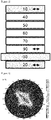
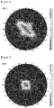
- omnidirectional CRs of the liquid crystal display of Experimental Example 3 above were illustrated in FIG. 5 below
- omnidirectional CRs of the liquid crystal display of Experimental Example 4 above were illustrated in FIG. 6 below
- omnidirectional CRs of the liquid crystal display of Experimental Example 5 above were illustrated in FIG. 7 below.
- absorption axes of the upper polarizer and the lower polarizer of the liquid crystal display are provided to be parallel to each other, thereby resolving a size limitation of the polarizer according to the width of the polarizer raw material.
- a first polarization rotation layer, a positive C plate, and a second polarization rotation layer are comprised between an upper polarizer and a liquid crystal panel, and as a result, black luminance is reduced due to scattering of side light to increase a front contrast ratio (CR) as compared with a case (not according to the claimed invention) where the first polarization rotation layer, the positive C plate, and the second polarization rotation layer are provided between a lower polarizer and the liquid crystal panel.
- CR front contrast ratio
- the positive C plate is comprised between the first polarization rotation layer and the second polarization rotation layer to minimize reduction of the contrast ratio (CR) at the viewing angle.
Landscapes
- Physics & Mathematics (AREA)
- Nonlinear Science (AREA)
- General Physics & Mathematics (AREA)
- Optics & Photonics (AREA)
- Mathematical Physics (AREA)
- Chemical & Material Sciences (AREA)
- Crystallography & Structural Chemistry (AREA)
- Spectroscopy & Molecular Physics (AREA)
- Liquid Crystal (AREA)
- Polarising Elements (AREA)
- Laminated Bodies (AREA)
Claims (14)
- Stratifié comprenant :une première couche de rotation de polarisation ;une deuxième couche de rotation de polarisation ; etune plaque C positive (60) fournie entre la première couche de rotation de polarisation et la deuxième couche de rotation de polarisation,dans lequel la première couche de rotation de polarisation comprend une première plaque demi-onde (40) et une première plaque quart d'onde (50), et la deuxième couche de rotation de polarisation comprend une deuxième plaque demi-onde (70) et une deuxième plaque quart d'onde (80), etdans lequel une valeur de retard dans la direction de l'épaisseur Rth de la plaque C positive (60) représentée par l'Équation 1 ci-dessous, pour une lumière ayant une longueur d'onde de 550 nm, est comprise entre 50 nm et 200 nm et une valeur de retard du front Ro représentée par l'Équation 2 ci-dessous, pour une lumière ayant une longueur d'onde de 550 nm, est comprise entre -5 nm et 5 nm :

 nx représente un indice de réfraction dans une direction dans laquelle l'indice de réfraction dans le plan de la plaque C positive (60) devient maximal,ny représente un indice de réfraction dans une direction perpendiculaire à la direction dans le plan de nx de la plaque C positive (60),nz représente l'indice de réfraction dans la direction de l'épaisseur de la plaque C positive (60), etd représente une épaisseur de la plaque C positive (60).
 - Stratifié selon la revendication 1, dans lequel la première plaque quart d'onde (50) de la première couche de rotation de polarisation est fournie sur la plaque C positive (60), et
dans lequel la deuxième plaque quart d'onde (80) de la deuxième couche de rotation de polarisation est fournie sur la plaque C positive (60). - Stratifié selon la revendication 1, dans lequel une valeur de Ro(450) / Ro(550) de la première plaque quart d'onde (50) est supérieure à une valeur de Ro(450) / Ro(550) de la première plaque demi-onde (40),la valeur de Ro(450) / Ro(550) de la deuxième plaque quart d'onde (80) est supérieure à la valeur de Ro(450) / Ro(550) de la deuxième plaque demi-onde (70),dans lequel Ro(450) indique la valeur de retard du front pour une lumière ayant une longueur d'onde de 450 nm, Ro(550) indique la valeur de retard du front pour une lumière ayant une longueur d'onde de 550 nm, et la valeur de retard du front Ro est représentée par l'Équation 8 ci-dessous :
 nx représente un indice de réfraction dans une direction dans laquelle l'indice de réfraction dans le plan de respectivement soit la première plaque demi-onde (40), soit la deuxième plaque demi-onde (70), soit la première plaque quart d'onde (50), soit la deuxième plaque quart d'onde (80) devient maximal,ny représente un indice de réfraction dans une direction perpendiculaire à la direction dans le plan de nx de respectivement soit la première plaque demi-onde (40), soit la deuxième plaque demi-onde (70), soit la première plaque quart d'onde (50), soit la deuxième plaque quart d'onde (80), etd représente une épaisseur de respectivement soit la première plaque demi-onde (40), soit la deuxième plaque demi-onde (70), soit la première plaque quart d'onde (50), soit la deuxième plaque quart d'onde (80).
 - Affichage à cristaux liquides comprenant :un polariseur supérieur (10) ;un polariseur inférieur (20) ; etun panneau à cristaux liquides (30) fourni entre le polariseur supérieur (10) et le polariseur inférieur (20),dans lequel le polariseur supérieur (10) et le polariseur inférieur (20) sont fournis de telle sorte que leurs axes d'absorption sont parallèles l'un à l'autre,dans lequel une première couche de rotation de polarisation, une plaque C positive (60) et une deuxième couche de rotation de polarisation sont comprises séquentiellement dans cet ordre entre le polariseur supérieur (10) et le panneau à cristaux liquides (30),dans lequel la première couche de rotation de polarisation comprend une première plaque demi-onde (40) et une première plaque quart d'onde (50), et la deuxième couche de rotation de polarisation comprend une deuxième plaque demi-onde (70) et une deuxième plaque quart d'onde (80), etdans lequel le panneau à cristaux liquides (30) a un mode à cristaux liquides à alignement vertical.
- Afficheur à cristaux liquides selon la revendication 4, dans lequel la première plaque quart d'onde (50) de la première couche de rotation de polarisation est fournie sur la plaque C positive (60), et
dans lequel la deuxième plaque quart d'onde (80) de la deuxième couche de rotation de polarisation est fournie sur la plaque C positive (60). - Afficheur à cristaux liquides selon la revendication 4, dans lequel un angle formé entre un axe optique de la première plaque demi-onde (40) de la première couche de rotation de polarisation et un axe d'absorption du polariseur supérieur (10) est compris entre 10 degrés et 20 degrés, et
dans lequel l'angle formé entre l'axe optique de la première plaque quart d'onde (50) de la première couche de rotation de polarisation et l'axe d'absorption du polariseur supérieur (10) est compris entre 70 degrés et 80 degrés. - Afficheur à cristaux liquides selon la revendication 4, dans lequel l'angle formé entre l'axe optique de la deuxième plaque quart d'onde (80) de la deuxième couche de rotation de polarisation et l'axe d'absorption du polariseur supérieur (10) est compris entre 10 degrés et 20 degrés, et
dans lequel l'angle formé entre l'axe optique de la deuxième plaque demi-onde (70) de la deuxième couche de rotation de polarisation et l'axe d'absorption du polariseur supérieur (10) est compris entre 70 degrés et 80 degrés. - Afficheur à cristaux liquides selon la revendication 4, dans lequel une valeur de retard dans la direction de l'épaisseur Rth de la plaque C positive (60) représentée par l'Équation 1 ci-dessous, pour une lumière ayant une longueur d'onde de 550 nm, est comprise entre 50 nm et 200 nm et une valeur de retard du front Ro représentée par l'Équation 2 ci-dessous, pour une lumière ayant une longueur d'onde de 550 nm, est comprise entre -5 nm et 5 nm :

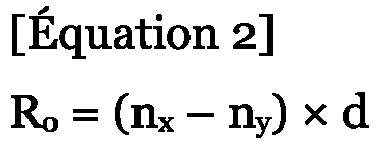 nx représente un indice de réfraction dans une direction dans laquelle l'indice de réfraction dans le plan de la plaque C positive (60) devient maximal,ny représente un indice de réfraction dans une direction perpendiculaire à la direction dans le plan de nx de la plaque C positive (60),nz représente l'indice de réfraction dans la direction de l'épaisseur de la plaque C positive (60), etd représente une épaisseur de la plaque C positive (60).
 - Afficheur à cristaux liquides selon la revendication 4, comprenant en outre :
un premier film de compensation d'angle de visualisation entre la deuxième couche de rotation de polarisation et le panneau à cristaux liquides (30). - Afficheur à cristaux liquides selon la revendication 9, dans lequel le premier film de compensation d'angle de visualisation comprend une plaque B négative (90).
- Afficheur à cristaux liquides selon la revendication 4, comprenant en outre :
un deuxième film de compensation d'angle de visualisation entre le panneau à cristaux liquides (30) et le polariseur inférieur (20). - Afficheur à cristaux liquides selon la revendication 11, dans lequel le deuxième film de compensation d'angle de visualisation comprend une plaque A positive et une plaque C négative.
- Afficheur à cristaux liquides selon la revendication 4, dans lequel chacune de la première plaque demi-onde (40), la deuxième plaque demi-onde (70), la première plaque quart d'onde (50) et la deuxième plaque quart d'onde (80) a une dispersibilité constante,
dans lequel la dispersibilité constante indique une caractéristique où, à mesure que la longueur d'onde de lumière incidente augmente, la valeur de retard générée diminue. - Afficheur à cristaux liquides selon la revendication 4, dans lequel une valeur de Ro(450) / Ro(550) de la première plaque quart d'onde (50) est supérieure à une valeur de Ro(450) / Ro(550) de la première plaque demi-onde (40),dans lequel la valeur de Ro(450) / Ro(550) de la deuxième plaque quart d'onde (80) est supérieure à la valeur de Ro(450) / Ro(550) de la deuxième plaque demi-onde (70), etdans lequel Ro(450) indique la valeur de retard du front pour une lumière ayant une longueur d'onde de 450 nm, Ro(550) indique la valeur de retard du front pour une lumière ayant une longueur d'onde de 550 nm, et la valeur de retard du front Ro est représentée par l'Équation 8 ci-dessous :
 nx représente un indice de réfraction dans une direction dans laquelle l'indice de réfraction dans le plan de respectivement soit la première plaque demi-onde (40), soit la deuxième plaque demi-onde (70), soit la première plaque quart d'onde (50), soit la deuxième plaque quart d'onde (80) devient maximal,ny représente un indice de réfraction dans une direction perpendiculaire à la direction dans le plan de nx de respectivement soit la première plaque demi-onde (40), soit la deuxième plaque demi-onde (70), soit la première plaque quart d'onde (50), soit la deuxième plaque quart d'onde (80), etd représente une épaisseur de respectivement soit la première plaque demi-onde (40), soit la deuxième plaque demi-onde (70), soit la première plaque quart d'onde (50), soit la deuxième plaque quart d'onde (80).
Applications Claiming Priority (2)
| Application Number | Priority Date | Filing Date | Title |
|---|---|---|---|
| KR20180064884 | 2018-06-05 | ||
| PCT/KR2019/006713 WO2019235809A1 (fr) | 2018-06-05 | 2019-06-04 | Empilement et dispositif d'affichage à cristaux liquides comprenant ce dernier |
Publications (3)
| Publication Number | Publication Date |
|---|---|
| EP3677958A1 EP3677958A1 (fr) | 2020-07-08 |
| EP3677958A4 EP3677958A4 (fr) | 2020-09-02 |
| EP3677958B1 true EP3677958B1 (fr) | 2023-01-18 |
Family
ID=68769741
Family Applications (1)
| Application Number | Title | Priority Date | Filing Date |
|---|---|---|---|
| EP19815371.0A Active EP3677958B1 (fr) | 2018-06-05 | 2019-06-04 | Empilement et dispositif d'affichage à cristaux liquides comprenant ce dernier |
Country Status (7)
| Country | Link |
|---|---|
| US (1) | US11022845B2 (fr) |
| EP (1) | EP3677958B1 (fr) |
| JP (1) | JP7123468B2 (fr) |
| KR (1) | KR102174676B1 (fr) |
| CN (1) | CN111201484B (fr) |
| TW (1) | TWI690414B (fr) |
| WO (1) | WO2019235809A1 (fr) |
Families Citing this family (8)
| Publication number | Priority date | Publication date | Assignee | Title |
|---|---|---|---|---|
| US12230782B2 (en) | 2018-11-02 | 2025-02-18 | Lg Energy Solution, Ltd. | Lithium secondary battery |
| EP4661097A3 (fr) | 2018-11-02 | 2026-01-14 | LG Energy Solution, Ltd. | Batterie secondaire au lithium |
| CN111897158B (zh) * | 2020-06-30 | 2023-04-25 | 上海天马微电子有限公司 | 液晶显示面板及显示装置 |
| KR20220108850A (ko) * | 2021-01-27 | 2022-08-04 | 삼성디스플레이 주식회사 | 광학 필름 및 이를 포함하는 표시 장치 |
| KR102950070B1 (ko) * | 2021-07-16 | 2026-04-08 | 동우 화인켐 주식회사 | 광학 적층체 및 이의 제조방법과, 이를 포함하는 스마트 윈도우 및 이를 적용한 자동차 또는 건물용 창호 |
| CN113820779B (zh) * | 2021-08-30 | 2023-03-10 | 华为技术有限公司 | 偏光片及其制备方法、显示面板 |
| JP2024104972A (ja) * | 2023-01-25 | 2024-08-06 | シャープディスプレイテクノロジー株式会社 | 液晶パネル及び表示装置 |
| CN118689008B (zh) * | 2024-07-11 | 2025-09-16 | 杉金光电(南京)有限公司 | 一种面内切换液晶显示器 |
Family Cites Families (31)
| Publication number | Priority date | Publication date | Assignee | Title |
|---|---|---|---|---|
| WO2003091766A1 (fr) | 2002-04-23 | 2003-11-06 | Nitto Denko Corporation | Polariseur, source de lumiere polarisante et unite d'affichage d'images utilisant ceux-ci |
| CN100399075C (zh) * | 2002-04-23 | 2008-07-02 | 日东电工株式会社 | 偏振部件,偏振光源及使用其的图像显示装置 |
| JP3834012B2 (ja) * | 2002-04-24 | 2006-10-18 | 日東電工株式会社 | 視野角拡大液晶表示装置 |
| JP2006268007A (ja) | 2005-02-25 | 2006-10-05 | Nitto Denko Corp | 楕円偏光板の製造方法および楕円偏光板を用いた画像表示装置 |
| KR101293564B1 (ko) * | 2005-07-27 | 2013-08-06 | 삼성디스플레이 주식회사 | 액정표시장치 |
| KR101157963B1 (ko) * | 2005-09-28 | 2012-06-25 | 엘지디스플레이 주식회사 | 액정표시장치 |
| KR20070081259A (ko) * | 2006-02-10 | 2007-08-16 | 삼성전자주식회사 | 액정 표시 장치 |
| US20090002609A1 (en) | 2007-05-18 | 2009-01-01 | Mitsutaka Okita | Liquid crystal display device |
| JP2009003432A (ja) | 2007-05-18 | 2009-01-08 | Toshiba Matsushita Display Technology Co Ltd | 液晶表示装置 |
| US20080309854A1 (en) * | 2007-06-15 | 2008-12-18 | Zhibing Ge | Wide Viewing Angle and Broadband Circular Polarizers for Transflective Liquid Crystal Displays |
| WO2009008406A1 (fr) * | 2007-07-09 | 2009-01-15 | Sharp Kabushiki Kaisha | Elément de commande d'angle de vision et dispositif d'affichage comportant celui-ci |
| JP2009031402A (ja) | 2007-07-25 | 2009-02-12 | Sumitomo Chemical Co Ltd | 液晶表示装置 |
| JP5893256B2 (ja) * | 2011-03-29 | 2016-03-23 | 株式会社ジャパンディスプレイ | 表示装置および電子機器 |
| JP2012252084A (ja) * | 2011-06-01 | 2012-12-20 | Nitto Denko Corp | 液晶パネルおよび液晶表示装置 |
| TWI457675B (zh) | 2011-08-29 | 2014-10-21 | Au Optronics Corp | 畫素結構、液晶顯示面板與透明液晶顯示器 |
| KR20130074878A (ko) * | 2011-12-27 | 2013-07-05 | 동우 화인켐 주식회사 | 반투과형 수직 배향 모드 액정표시장치 |
| KR102000145B1 (ko) * | 2013-01-04 | 2019-07-16 | 엘지디스플레이 주식회사 | 광시야각 액정표시장치 |
| JP2015025830A (ja) * | 2013-03-29 | 2015-02-05 | 富士フイルム株式会社 | 液晶表示装置 |
| KR20150007518A (ko) * | 2013-07-11 | 2015-01-21 | 동우 화인켐 주식회사 | 액정 패널 및 이를 구비하는 액정 표시 장치 |
| JP6175972B2 (ja) * | 2013-08-20 | 2017-08-09 | 大日本印刷株式会社 | 光学フィルム、画像表示装置、光学フィルム用転写体、光学フィルムの製造方法及び光学フィルム用転写体の製造方法 |
| JP2015079230A (ja) | 2013-09-10 | 2015-04-23 | 住友化学株式会社 | 積層体の製造方法 |
| KR20150122410A (ko) * | 2014-04-23 | 2015-11-02 | 동우 화인켐 주식회사 | 편광판 및 이를 포함하는 액정표시장치 |
| WO2016043124A1 (fr) * | 2014-09-17 | 2016-03-24 | 日本ゼオン株式会社 | Plaque polarisante circulaire, plaque λ/4 à large bande et dispositif d'affichage à électroluminescence organique |
| KR101790404B1 (ko) | 2015-02-25 | 2017-10-26 | 주식회사 엘지화학 | 편광자의 제조방법, 이를 이용하여 제조된 편광자, 이를 포함하는 편광판 및 화상표시장치 |
| KR20160112380A (ko) | 2015-03-19 | 2016-09-28 | 동우 화인켐 주식회사 | 액정 패널 및 이를 구비하는 액정 표시 장치 |
| WO2016171169A1 (fr) * | 2015-04-21 | 2016-10-27 | 日本ゼオン株式会社 | Film multicouche et son procédé de fabrication, procédé de fabrication de corps de transfert optiquement anisotrope, couche optiquement anisotrope, élément optiquement anisotrope, et corps stratifié optique |
| US10816710B2 (en) * | 2016-03-18 | 2020-10-27 | Samsung Sdi Co., Ltd. | Polarizing plate for light emitting display device and light emitting display device including same |
| JPWO2017170346A1 (ja) * | 2016-03-30 | 2019-02-14 | 日本ゼオン株式会社 | 円偏光板及び画像表示装置 |
| JP2018060152A (ja) * | 2016-05-27 | 2018-04-12 | 住友化学株式会社 | Ipsモード用の偏光板のセット及びそれを用いたipsモード液晶表示装置 |
| EP3264147B1 (fr) * | 2016-06-30 | 2024-05-08 | LG Display Co., Ltd. | Procédé de fabrication d'un polariseur |
| KR20180064884A (ko) | 2016-12-06 | 2018-06-15 | 한국전자통신연구원 | 홀로그램 기술 기반의 광학 콘볼루션 뉴럴 네트워크 시스템 |
-
2019
- 2019-06-04 EP EP19815371.0A patent/EP3677958B1/fr active Active
- 2019-06-04 US US16/758,369 patent/US11022845B2/en active Active
- 2019-06-04 CN CN201980004990.7A patent/CN111201484B/zh active Active
- 2019-06-04 KR KR1020190065941A patent/KR102174676B1/ko active Active
- 2019-06-04 JP JP2020524008A patent/JP7123468B2/ja active Active
- 2019-06-04 WO PCT/KR2019/006713 patent/WO2019235809A1/fr not_active Ceased
- 2019-06-04 TW TW108119379A patent/TWI690414B/zh active
Also Published As
| Publication number | Publication date |
|---|---|
| CN111201484B (zh) | 2022-10-11 |
| TWI690414B (zh) | 2020-04-11 |
| EP3677958A4 (fr) | 2020-09-02 |
| JP7123468B2 (ja) | 2022-08-23 |
| EP3677958A1 (fr) | 2020-07-08 |
| US11022845B2 (en) | 2021-06-01 |
| CN111201484A (zh) | 2020-05-26 |
| JP2021501366A (ja) | 2021-01-14 |
| KR102174676B1 (ko) | 2020-11-05 |
| TW202014306A (zh) | 2020-04-16 |
| KR20190138598A (ko) | 2019-12-13 |
| WO2019235809A1 (fr) | 2019-12-12 |
| US20200326573A1 (en) | 2020-10-15 |
Similar Documents
| Publication | Publication Date | Title |
|---|---|---|
| EP3677958B1 (fr) | Empilement et dispositif d'affichage à cristaux liquides comprenant ce dernier | |
| EP3677957B1 (fr) | Dispositif d'affichage à cristaux liquides | |
| EP3736621B1 (fr) | Dispositif d'affichage à cristaux liquides | |
| US11275266B2 (en) | Laminate and liquid crystal display device comprising same | |
| EP3805853B1 (fr) | Stratifié et dispositif d'affichage à cristaux liquides le comprenant |
Legal Events
| Date | Code | Title | Description |
|---|---|---|---|
| STAA | Information on the status of an ep patent application or granted ep patent |
Free format text: STATUS: THE INTERNATIONAL PUBLICATION HAS BEEN MADE |
|
| PUAI | Public reference made under article 153(3) epc to a published international application that has entered the european phase |
Free format text: ORIGINAL CODE: 0009012 |
|
| STAA | Information on the status of an ep patent application or granted ep patent |
Free format text: STATUS: REQUEST FOR EXAMINATION WAS MADE |
|
| 17P | Request for examination filed |
Effective date: 20200401 |
|
| AK | Designated contracting states |
Kind code of ref document: A1 Designated state(s): AL AT BE BG CH CY CZ DE DK EE ES FI FR GB GR HR HU IE IS IT LI LT LU LV MC MK MT NL NO PL PT RO RS SE SI SK SM TR |
|
| AX | Request for extension of the european patent |
Extension state: BA ME |
|
| A4 | Supplementary search report drawn up and despatched |
Effective date: 20200803 |
|
| RIC1 | Information provided on ipc code assigned before grant |
Ipc: G02F 1/13363 20060101AFI20200728BHEP Ipc: G02B 5/30 20060101ALI20200728BHEP Ipc: B32B 27/30 20060101ALI20200728BHEP Ipc: G02F 1/1335 20060101ALI20200728BHEP |
|
| DAV | Request for validation of the european patent (deleted) | ||
| DAX | Request for extension of the european patent (deleted) | ||
| GRAP | Despatch of communication of intention to grant a patent |
Free format text: ORIGINAL CODE: EPIDOSNIGR1 |
|
| STAA | Information on the status of an ep patent application or granted ep patent |
Free format text: STATUS: GRANT OF PATENT IS INTENDED |
|
| INTG | Intention to grant announced |
Effective date: 20220915 |
|
| GRAS | Grant fee paid |
Free format text: ORIGINAL CODE: EPIDOSNIGR3 |
|
| GRAA | (expected) grant |
Free format text: ORIGINAL CODE: 0009210 |
|
| STAA | Information on the status of an ep patent application or granted ep patent |
Free format text: STATUS: THE PATENT HAS BEEN GRANTED |
|
| AK | Designated contracting states |
Kind code of ref document: B1 Designated state(s): AL AT BE BG CH CY CZ DE DK EE ES FI FR GB GR HR HU IE IS IT LI LT LU LV MC MK MT NL NO PL PT RO RS SE SI SK SM TR |
|
| REG | Reference to a national code |
Ref country code: GB Ref legal event code: FG4D |
|
| REG | Reference to a national code |
Ref country code: CH Ref legal event code: EP |
|
| REG | Reference to a national code |
Ref country code: DE Ref legal event code: R096 Ref document number: 602019024611 Country of ref document: DE |
|
| REG | Reference to a national code |
Ref country code: AT Ref legal event code: REF Ref document number: 1545030 Country of ref document: AT Kind code of ref document: T Effective date: 20230215 Ref country code: IE Ref legal event code: FG4D |
|
| REG | Reference to a national code |
Ref country code: LT Ref legal event code: MG9D |
|
| REG | Reference to a national code |
Ref country code: NL Ref legal event code: MP Effective date: 20230118 |
|
| REG | Reference to a national code |
Ref country code: AT Ref legal event code: MK05 Ref document number: 1545030 Country of ref document: AT Kind code of ref document: T Effective date: 20230118 |
|
| PG25 | Lapsed in a contracting state [announced via postgrant information from national office to epo] |
Ref country code: NL Free format text: LAPSE BECAUSE OF FAILURE TO SUBMIT A TRANSLATION OF THE DESCRIPTION OR TO PAY THE FEE WITHIN THE PRESCRIBED TIME-LIMIT Effective date: 20230118 |
|
| PG25 | Lapsed in a contracting state [announced via postgrant information from national office to epo] |
Ref country code: RS Free format text: LAPSE BECAUSE OF FAILURE TO SUBMIT A TRANSLATION OF THE DESCRIPTION OR TO PAY THE FEE WITHIN THE PRESCRIBED TIME-LIMIT Effective date: 20230118 Ref country code: PT Free format text: LAPSE BECAUSE OF FAILURE TO SUBMIT A TRANSLATION OF THE DESCRIPTION OR TO PAY THE FEE WITHIN THE PRESCRIBED TIME-LIMIT Effective date: 20230518 Ref country code: NO Free format text: LAPSE BECAUSE OF FAILURE TO SUBMIT A TRANSLATION OF THE DESCRIPTION OR TO PAY THE FEE WITHIN THE PRESCRIBED TIME-LIMIT Effective date: 20230418 Ref country code: LV Free format text: LAPSE BECAUSE OF FAILURE TO SUBMIT A TRANSLATION OF THE DESCRIPTION OR TO PAY THE FEE WITHIN THE PRESCRIBED TIME-LIMIT Effective date: 20230118 Ref country code: LT Free format text: LAPSE BECAUSE OF FAILURE TO SUBMIT A TRANSLATION OF THE DESCRIPTION OR TO PAY THE FEE WITHIN THE PRESCRIBED TIME-LIMIT Effective date: 20230118 Ref country code: HR Free format text: LAPSE BECAUSE OF FAILURE TO SUBMIT A TRANSLATION OF THE DESCRIPTION OR TO PAY THE FEE WITHIN THE PRESCRIBED TIME-LIMIT Effective date: 20230118 Ref country code: ES Free format text: LAPSE BECAUSE OF FAILURE TO SUBMIT A TRANSLATION OF THE DESCRIPTION OR TO PAY THE FEE WITHIN THE PRESCRIBED TIME-LIMIT Effective date: 20230118 Ref country code: AT Free format text: LAPSE BECAUSE OF FAILURE TO SUBMIT A TRANSLATION OF THE DESCRIPTION OR TO PAY THE FEE WITHIN THE PRESCRIBED TIME-LIMIT Effective date: 20230118 |
|
| PG25 | Lapsed in a contracting state [announced via postgrant information from national office to epo] |
Ref country code: SE Free format text: LAPSE BECAUSE OF FAILURE TO SUBMIT A TRANSLATION OF THE DESCRIPTION OR TO PAY THE FEE WITHIN THE PRESCRIBED TIME-LIMIT Effective date: 20230118 Ref country code: PL Free format text: LAPSE BECAUSE OF FAILURE TO SUBMIT A TRANSLATION OF THE DESCRIPTION OR TO PAY THE FEE WITHIN THE PRESCRIBED TIME-LIMIT Effective date: 20230118 Ref country code: IS Free format text: LAPSE BECAUSE OF FAILURE TO SUBMIT A TRANSLATION OF THE DESCRIPTION OR TO PAY THE FEE WITHIN THE PRESCRIBED TIME-LIMIT Effective date: 20230518 Ref country code: GR Free format text: LAPSE BECAUSE OF FAILURE TO SUBMIT A TRANSLATION OF THE DESCRIPTION OR TO PAY THE FEE WITHIN THE PRESCRIBED TIME-LIMIT Effective date: 20230419 Ref country code: FI Free format text: LAPSE BECAUSE OF FAILURE TO SUBMIT A TRANSLATION OF THE DESCRIPTION OR TO PAY THE FEE WITHIN THE PRESCRIBED TIME-LIMIT Effective date: 20230118 |
|
| REG | Reference to a national code |
Ref country code: DE Ref legal event code: R097 Ref document number: 602019024611 Country of ref document: DE |
|
| PG25 | Lapsed in a contracting state [announced via postgrant information from national office to epo] |
Ref country code: SM Free format text: LAPSE BECAUSE OF FAILURE TO SUBMIT A TRANSLATION OF THE DESCRIPTION OR TO PAY THE FEE WITHIN THE PRESCRIBED TIME-LIMIT Effective date: 20230118 Ref country code: RO Free format text: LAPSE BECAUSE OF FAILURE TO SUBMIT A TRANSLATION OF THE DESCRIPTION OR TO PAY THE FEE WITHIN THE PRESCRIBED TIME-LIMIT Effective date: 20230118 Ref country code: EE Free format text: LAPSE BECAUSE OF FAILURE TO SUBMIT A TRANSLATION OF THE DESCRIPTION OR TO PAY THE FEE WITHIN THE PRESCRIBED TIME-LIMIT Effective date: 20230118 Ref country code: DK Free format text: LAPSE BECAUSE OF FAILURE TO SUBMIT A TRANSLATION OF THE DESCRIPTION OR TO PAY THE FEE WITHIN THE PRESCRIBED TIME-LIMIT Effective date: 20230118 Ref country code: CZ Free format text: LAPSE BECAUSE OF FAILURE TO SUBMIT A TRANSLATION OF THE DESCRIPTION OR TO PAY THE FEE WITHIN THE PRESCRIBED TIME-LIMIT Effective date: 20230118 |
|
| PLBE | No opposition filed within time limit |
Free format text: ORIGINAL CODE: 0009261 |
|
| STAA | Information on the status of an ep patent application or granted ep patent |
Free format text: STATUS: NO OPPOSITION FILED WITHIN TIME LIMIT |
|
| PG25 | Lapsed in a contracting state [announced via postgrant information from national office to epo] |
Ref country code: SK Free format text: LAPSE BECAUSE OF FAILURE TO SUBMIT A TRANSLATION OF THE DESCRIPTION OR TO PAY THE FEE WITHIN THE PRESCRIBED TIME-LIMIT Effective date: 20230118 |
|
| 26N | No opposition filed |
Effective date: 20231019 |
|
| PG25 | Lapsed in a contracting state [announced via postgrant information from national office to epo] |
Ref country code: MC Free format text: LAPSE BECAUSE OF FAILURE TO SUBMIT A TRANSLATION OF THE DESCRIPTION OR TO PAY THE FEE WITHIN THE PRESCRIBED TIME-LIMIT Effective date: 20230118 |
|
| PG25 | Lapsed in a contracting state [announced via postgrant information from national office to epo] |
Ref country code: SI Free format text: LAPSE BECAUSE OF FAILURE TO SUBMIT A TRANSLATION OF THE DESCRIPTION OR TO PAY THE FEE WITHIN THE PRESCRIBED TIME-LIMIT Effective date: 20230118 Ref country code: MC Free format text: LAPSE BECAUSE OF FAILURE TO SUBMIT A TRANSLATION OF THE DESCRIPTION OR TO PAY THE FEE WITHIN THE PRESCRIBED TIME-LIMIT Effective date: 20230118 |
|
| REG | Reference to a national code |
Ref country code: CH Ref legal event code: PL |
|
| REG | Reference to a national code |
Ref country code: BE Ref legal event code: MM Effective date: 20230630 |
|
| PG25 | Lapsed in a contracting state [announced via postgrant information from national office to epo] |
Ref country code: LU Free format text: LAPSE BECAUSE OF NON-PAYMENT OF DUE FEES Effective date: 20230604 |
|
| REG | Reference to a national code |
Ref country code: IE Ref legal event code: MM4A |
|
| PG25 | Lapsed in a contracting state [announced via postgrant information from national office to epo] |
Ref country code: LU Free format text: LAPSE BECAUSE OF NON-PAYMENT OF DUE FEES Effective date: 20230604 |
|
| PG25 | Lapsed in a contracting state [announced via postgrant information from national office to epo] |
Ref country code: IE Free format text: LAPSE BECAUSE OF NON-PAYMENT OF DUE FEES Effective date: 20230604 |
|
| PG25 | Lapsed in a contracting state [announced via postgrant information from national office to epo] |
Ref country code: IE Free format text: LAPSE BECAUSE OF NON-PAYMENT OF DUE FEES Effective date: 20230604 Ref country code: CH Free format text: LAPSE BECAUSE OF NON-PAYMENT OF DUE FEES Effective date: 20230630 |
|
| PG25 | Lapsed in a contracting state [announced via postgrant information from national office to epo] |
Ref country code: IT Free format text: LAPSE BECAUSE OF FAILURE TO SUBMIT A TRANSLATION OF THE DESCRIPTION OR TO PAY THE FEE WITHIN THE PRESCRIBED TIME-LIMIT Effective date: 20230118 Ref country code: BE Free format text: LAPSE BECAUSE OF NON-PAYMENT OF DUE FEES Effective date: 20230630 |
|
| PG25 | Lapsed in a contracting state [announced via postgrant information from national office to epo] |
Ref country code: BG Free format text: LAPSE BECAUSE OF FAILURE TO SUBMIT A TRANSLATION OF THE DESCRIPTION OR TO PAY THE FEE WITHIN THE PRESCRIBED TIME-LIMIT Effective date: 20230118 |
|
| PG25 | Lapsed in a contracting state [announced via postgrant information from national office to epo] |
Ref country code: BG Free format text: LAPSE BECAUSE OF FAILURE TO SUBMIT A TRANSLATION OF THE DESCRIPTION OR TO PAY THE FEE WITHIN THE PRESCRIBED TIME-LIMIT Effective date: 20230118 |
|
| PGFP | Annual fee paid to national office [announced via postgrant information from national office to epo] |
Ref country code: DE Payment date: 20250417 Year of fee payment: 7 |
|
| PGFP | Annual fee paid to national office [announced via postgrant information from national office to epo] |
Ref country code: GB Payment date: 20250416 Year of fee payment: 7 |
|
| PGFP | Annual fee paid to national office [announced via postgrant information from national office to epo] |
Ref country code: FR Payment date: 20250416 Year of fee payment: 7 |
|
| PG25 | Lapsed in a contracting state [announced via postgrant information from national office to epo] |
Ref country code: CY Free format text: LAPSE BECAUSE OF FAILURE TO SUBMIT A TRANSLATION OF THE DESCRIPTION OR TO PAY THE FEE WITHIN THE PRESCRIBED TIME-LIMIT; INVALID AB INITIO Effective date: 20190604 |
|
| PG25 | Lapsed in a contracting state [announced via postgrant information from national office to epo] |
Ref country code: HU Free format text: LAPSE BECAUSE OF FAILURE TO SUBMIT A TRANSLATION OF THE DESCRIPTION OR TO PAY THE FEE WITHIN THE PRESCRIBED TIME-LIMIT; INVALID AB INITIO Effective date: 20190604 |
|
| REG | Reference to a national code |
Ref country code: GB Ref legal event code: 732E Free format text: REGISTERED BETWEEN 20250918 AND 20250924 |
|
| REG | Reference to a national code |
Ref country code: DE Ref legal event code: R081 Ref document number: 602019024611 Country of ref document: DE Owner name: SHANJIN OPTOELECTRONICS (SUZHOU) CO., LTD., ZH, CN Free format text: FORMER OWNER: LG CHEM, LTD., SEOUL, KR |
|
| PG25 | Lapsed in a contracting state [announced via postgrant information from national office to epo] |
Ref country code: TR Free format text: LAPSE BECAUSE OF FAILURE TO SUBMIT A TRANSLATION OF THE DESCRIPTION OR TO PAY THE FEE WITHIN THE PRESCRIBED TIME-LIMIT Effective date: 20230118 |