EP3736621B1 - Dispositif d'affichage à cristaux liquides - Google Patents
Dispositif d'affichage à cristaux liquides Download PDFInfo
- Publication number
- EP3736621B1 EP3736621B1 EP18898754.9A EP18898754A EP3736621B1 EP 3736621 B1 EP3736621 B1 EP 3736621B1 EP 18898754 A EP18898754 A EP 18898754A EP 3736621 B1 EP3736621 B1 EP 3736621B1
- Authority
- EP
- European Patent Office
- Prior art keywords
- liquid crystal
- polarizer
- degrees
- crystal panel
- wave plate
- Prior art date
- Legal status (The legal status is an assumption and is not a legal conclusion. Google has not performed a legal analysis and makes no representation as to the accuracy of the status listed.)
- Active
Links
Images





Classifications
-
- G—PHYSICS
- G02—OPTICS
- G02F—OPTICAL DEVICES OR ARRANGEMENTS FOR THE CONTROL OF LIGHT BY MODIFICATION OF THE OPTICAL PROPERTIES OF THE MEDIA OF THE ELEMENTS INVOLVED THEREIN; NON-LINEAR OPTICS; FREQUENCY-CHANGING OF LIGHT; OPTICAL LOGIC ELEMENTS; OPTICAL ANALOGUE/DIGITAL CONVERTERS
- G02F1/00—Devices or arrangements for the control of the intensity, colour, phase, polarisation or direction of light arriving from an independent light source, e.g. switching, gating or modulating; Non-linear optics
- G02F1/01—Devices or arrangements for the control of the intensity, colour, phase, polarisation or direction of light arriving from an independent light source, e.g. switching, gating or modulating; Non-linear optics for the control of the intensity, phase, polarisation or colour
- G02F1/13—Devices or arrangements for the control of the intensity, colour, phase, polarisation or direction of light arriving from an independent light source, e.g. switching, gating or modulating; Non-linear optics for the control of the intensity, phase, polarisation or colour based on liquid crystals, e.g. single liquid crystal display cells
- G02F1/133—Constructional arrangements; Operation of liquid crystal cells; Circuit arrangements
- G02F1/1333—Constructional arrangements; Manufacturing methods
- G02F1/1335—Structural association of cells with optical devices, e.g. polarisers or reflectors
- G02F1/13363—Birefringent elements, e.g. for optical compensation
- G02F1/133634—Birefringent elements, e.g. for optical compensation the refractive index Nz perpendicular to the element surface being different from in-plane refractive indices Nx and Ny, e.g. biaxial or with normal optical axis
-
- G—PHYSICS
- G02—OPTICS
- G02F—OPTICAL DEVICES OR ARRANGEMENTS FOR THE CONTROL OF LIGHT BY MODIFICATION OF THE OPTICAL PROPERTIES OF THE MEDIA OF THE ELEMENTS INVOLVED THEREIN; NON-LINEAR OPTICS; FREQUENCY-CHANGING OF LIGHT; OPTICAL LOGIC ELEMENTS; OPTICAL ANALOGUE/DIGITAL CONVERTERS
- G02F1/00—Devices or arrangements for the control of the intensity, colour, phase, polarisation or direction of light arriving from an independent light source, e.g. switching, gating or modulating; Non-linear optics
- G02F1/01—Devices or arrangements for the control of the intensity, colour, phase, polarisation or direction of light arriving from an independent light source, e.g. switching, gating or modulating; Non-linear optics for the control of the intensity, phase, polarisation or colour
- G02F1/13—Devices or arrangements for the control of the intensity, colour, phase, polarisation or direction of light arriving from an independent light source, e.g. switching, gating or modulating; Non-linear optics for the control of the intensity, phase, polarisation or colour based on liquid crystals, e.g. single liquid crystal display cells
- G02F1/133—Constructional arrangements; Operation of liquid crystal cells; Circuit arrangements
- G02F1/1333—Constructional arrangements; Manufacturing methods
- G02F1/1335—Structural association of cells with optical devices, e.g. polarisers or reflectors
- G02F1/133528—Polarisers
-
- G—PHYSICS
- G02—OPTICS
- G02F—OPTICAL DEVICES OR ARRANGEMENTS FOR THE CONTROL OF LIGHT BY MODIFICATION OF THE OPTICAL PROPERTIES OF THE MEDIA OF THE ELEMENTS INVOLVED THEREIN; NON-LINEAR OPTICS; FREQUENCY-CHANGING OF LIGHT; OPTICAL LOGIC ELEMENTS; OPTICAL ANALOGUE/DIGITAL CONVERTERS
- G02F1/00—Devices or arrangements for the control of the intensity, colour, phase, polarisation or direction of light arriving from an independent light source, e.g. switching, gating or modulating; Non-linear optics
- G02F1/01—Devices or arrangements for the control of the intensity, colour, phase, polarisation or direction of light arriving from an independent light source, e.g. switching, gating or modulating; Non-linear optics for the control of the intensity, phase, polarisation or colour
- G02F1/13—Devices or arrangements for the control of the intensity, colour, phase, polarisation or direction of light arriving from an independent light source, e.g. switching, gating or modulating; Non-linear optics for the control of the intensity, phase, polarisation or colour based on liquid crystals, e.g. single liquid crystal display cells
- G02F1/133—Constructional arrangements; Operation of liquid crystal cells; Circuit arrangements
- G02F1/1333—Constructional arrangements; Manufacturing methods
- G02F1/1335—Structural association of cells with optical devices, e.g. polarisers or reflectors
- G02F1/13363—Birefringent elements, e.g. for optical compensation
- G02F1/133637—Birefringent elements, e.g. for optical compensation characterised by the wavelength dispersion
-
- G—PHYSICS
- G02—OPTICS
- G02F—OPTICAL DEVICES OR ARRANGEMENTS FOR THE CONTROL OF LIGHT BY MODIFICATION OF THE OPTICAL PROPERTIES OF THE MEDIA OF THE ELEMENTS INVOLVED THEREIN; NON-LINEAR OPTICS; FREQUENCY-CHANGING OF LIGHT; OPTICAL LOGIC ELEMENTS; OPTICAL ANALOGUE/DIGITAL CONVERTERS
- G02F1/00—Devices or arrangements for the control of the intensity, colour, phase, polarisation or direction of light arriving from an independent light source, e.g. switching, gating or modulating; Non-linear optics
- G02F1/01—Devices or arrangements for the control of the intensity, colour, phase, polarisation or direction of light arriving from an independent light source, e.g. switching, gating or modulating; Non-linear optics for the control of the intensity, phase, polarisation or colour
- G02F1/13—Devices or arrangements for the control of the intensity, colour, phase, polarisation or direction of light arriving from an independent light source, e.g. switching, gating or modulating; Non-linear optics for the control of the intensity, phase, polarisation or colour based on liquid crystals, e.g. single liquid crystal display cells
- G02F1/133—Constructional arrangements; Operation of liquid crystal cells; Circuit arrangements
- G02F1/1333—Constructional arrangements; Manufacturing methods
- G02F1/1335—Structural association of cells with optical devices, e.g. polarisers or reflectors
- G02F1/133528—Polarisers
- G02F1/133531—Polarisers characterised by the arrangement of polariser or analyser axes
-
- G—PHYSICS
- G02—OPTICS
- G02F—OPTICAL DEVICES OR ARRANGEMENTS FOR THE CONTROL OF LIGHT BY MODIFICATION OF THE OPTICAL PROPERTIES OF THE MEDIA OF THE ELEMENTS INVOLVED THEREIN; NON-LINEAR OPTICS; FREQUENCY-CHANGING OF LIGHT; OPTICAL LOGIC ELEMENTS; OPTICAL ANALOGUE/DIGITAL CONVERTERS
- G02F1/00—Devices or arrangements for the control of the intensity, colour, phase, polarisation or direction of light arriving from an independent light source, e.g. switching, gating or modulating; Non-linear optics
- G02F1/01—Devices or arrangements for the control of the intensity, colour, phase, polarisation or direction of light arriving from an independent light source, e.g. switching, gating or modulating; Non-linear optics for the control of the intensity, phase, polarisation or colour
- G02F1/13—Devices or arrangements for the control of the intensity, colour, phase, polarisation or direction of light arriving from an independent light source, e.g. switching, gating or modulating; Non-linear optics for the control of the intensity, phase, polarisation or colour based on liquid crystals, e.g. single liquid crystal display cells
- G02F1/133—Constructional arrangements; Operation of liquid crystal cells; Circuit arrangements
- G02F1/1333—Constructional arrangements; Manufacturing methods
- G02F1/1335—Structural association of cells with optical devices, e.g. polarisers or reflectors
- G02F1/13363—Birefringent elements, e.g. for optical compensation
-
- G—PHYSICS
- G02—OPTICS
- G02F—OPTICAL DEVICES OR ARRANGEMENTS FOR THE CONTROL OF LIGHT BY MODIFICATION OF THE OPTICAL PROPERTIES OF THE MEDIA OF THE ELEMENTS INVOLVED THEREIN; NON-LINEAR OPTICS; FREQUENCY-CHANGING OF LIGHT; OPTICAL LOGIC ELEMENTS; OPTICAL ANALOGUE/DIGITAL CONVERTERS
- G02F1/00—Devices or arrangements for the control of the intensity, colour, phase, polarisation or direction of light arriving from an independent light source, e.g. switching, gating or modulating; Non-linear optics
- G02F1/01—Devices or arrangements for the control of the intensity, colour, phase, polarisation or direction of light arriving from an independent light source, e.g. switching, gating or modulating; Non-linear optics for the control of the intensity, phase, polarisation or colour
- G02F1/13—Devices or arrangements for the control of the intensity, colour, phase, polarisation or direction of light arriving from an independent light source, e.g. switching, gating or modulating; Non-linear optics for the control of the intensity, phase, polarisation or colour based on liquid crystals, e.g. single liquid crystal display cells
- G02F1/133—Constructional arrangements; Operation of liquid crystal cells; Circuit arrangements
- G02F1/1333—Constructional arrangements; Manufacturing methods
- G02F1/1335—Structural association of cells with optical devices, e.g. polarisers or reflectors
- G02F1/13363—Birefringent elements, e.g. for optical compensation
- G02F1/133638—Waveplates, i.e. plates with a retardation value of lambda/n
-
- G—PHYSICS
- G02—OPTICS
- G02F—OPTICAL DEVICES OR ARRANGEMENTS FOR THE CONTROL OF LIGHT BY MODIFICATION OF THE OPTICAL PROPERTIES OF THE MEDIA OF THE ELEMENTS INVOLVED THEREIN; NON-LINEAR OPTICS; FREQUENCY-CHANGING OF LIGHT; OPTICAL LOGIC ELEMENTS; OPTICAL ANALOGUE/DIGITAL CONVERTERS
- G02F1/00—Devices or arrangements for the control of the intensity, colour, phase, polarisation or direction of light arriving from an independent light source, e.g. switching, gating or modulating; Non-linear optics
- G02F1/01—Devices or arrangements for the control of the intensity, colour, phase, polarisation or direction of light arriving from an independent light source, e.g. switching, gating or modulating; Non-linear optics for the control of the intensity, phase, polarisation or colour
- G02F1/13—Devices or arrangements for the control of the intensity, colour, phase, polarisation or direction of light arriving from an independent light source, e.g. switching, gating or modulating; Non-linear optics for the control of the intensity, phase, polarisation or colour based on liquid crystals, e.g. single liquid crystal display cells
- G02F1/133—Constructional arrangements; Operation of liquid crystal cells; Circuit arrangements
- G02F1/1333—Constructional arrangements; Manufacturing methods
- G02F1/1343—Electrodes
- G02F1/134309—Electrodes characterised by their geometrical arrangement
- G02F1/134363—Electrodes characterised by their geometrical arrangement for applying an electric field parallel to the substrate, i.e. in-plane switching [IPS]
-
- G—PHYSICS
- G02—OPTICS
- G02F—OPTICAL DEVICES OR ARRANGEMENTS FOR THE CONTROL OF LIGHT BY MODIFICATION OF THE OPTICAL PROPERTIES OF THE MEDIA OF THE ELEMENTS INVOLVED THEREIN; NON-LINEAR OPTICS; FREQUENCY-CHANGING OF LIGHT; OPTICAL LOGIC ELEMENTS; OPTICAL ANALOGUE/DIGITAL CONVERTERS
- G02F2203/00—Function characteristic
- G02F2203/01—Function characteristic transmissive
-
- G—PHYSICS
- G02—OPTICS
- G02F—OPTICAL DEVICES OR ARRANGEMENTS FOR THE CONTROL OF LIGHT BY MODIFICATION OF THE OPTICAL PROPERTIES OF THE MEDIA OF THE ELEMENTS INVOLVED THEREIN; NON-LINEAR OPTICS; FREQUENCY-CHANGING OF LIGHT; OPTICAL LOGIC ELEMENTS; OPTICAL ANALOGUE/DIGITAL CONVERTERS
- G02F2413/00—Indexing scheme related to G02F1/13363, i.e. to birefringent elements, e.g. for optical compensation, characterised by the number, position, orientation or value of the compensation plates
- G02F2413/01—Number of plates being 1
-
- G—PHYSICS
- G02—OPTICS
- G02F—OPTICAL DEVICES OR ARRANGEMENTS FOR THE CONTROL OF LIGHT BY MODIFICATION OF THE OPTICAL PROPERTIES OF THE MEDIA OF THE ELEMENTS INVOLVED THEREIN; NON-LINEAR OPTICS; FREQUENCY-CHANGING OF LIGHT; OPTICAL LOGIC ELEMENTS; OPTICAL ANALOGUE/DIGITAL CONVERTERS
- G02F2413/00—Indexing scheme related to G02F1/13363, i.e. to birefringent elements, e.g. for optical compensation, characterised by the number, position, orientation or value of the compensation plates
- G02F2413/02—Number of plates being 2
-
- G—PHYSICS
- G02—OPTICS
- G02F—OPTICAL DEVICES OR ARRANGEMENTS FOR THE CONTROL OF LIGHT BY MODIFICATION OF THE OPTICAL PROPERTIES OF THE MEDIA OF THE ELEMENTS INVOLVED THEREIN; NON-LINEAR OPTICS; FREQUENCY-CHANGING OF LIGHT; OPTICAL LOGIC ELEMENTS; OPTICAL ANALOGUE/DIGITAL CONVERTERS
- G02F2413/00—Indexing scheme related to G02F1/13363, i.e. to birefringent elements, e.g. for optical compensation, characterised by the number, position, orientation or value of the compensation plates
- G02F2413/03—Number of plates being 3
-
- G—PHYSICS
- G02—OPTICS
- G02F—OPTICAL DEVICES OR ARRANGEMENTS FOR THE CONTROL OF LIGHT BY MODIFICATION OF THE OPTICAL PROPERTIES OF THE MEDIA OF THE ELEMENTS INVOLVED THEREIN; NON-LINEAR OPTICS; FREQUENCY-CHANGING OF LIGHT; OPTICAL LOGIC ELEMENTS; OPTICAL ANALOGUE/DIGITAL CONVERTERS
- G02F2413/00—Indexing scheme related to G02F1/13363, i.e. to birefringent elements, e.g. for optical compensation, characterised by the number, position, orientation or value of the compensation plates
- G02F2413/04—Number of plates greater than or equal to 4
-
- G—PHYSICS
- G02—OPTICS
- G02F—OPTICAL DEVICES OR ARRANGEMENTS FOR THE CONTROL OF LIGHT BY MODIFICATION OF THE OPTICAL PROPERTIES OF THE MEDIA OF THE ELEMENTS INVOLVED THEREIN; NON-LINEAR OPTICS; FREQUENCY-CHANGING OF LIGHT; OPTICAL LOGIC ELEMENTS; OPTICAL ANALOGUE/DIGITAL CONVERTERS
- G02F2413/00—Indexing scheme related to G02F1/13363, i.e. to birefringent elements, e.g. for optical compensation, characterised by the number, position, orientation or value of the compensation plates
- G02F2413/07—All plates on one side of the LC cell
-
- G—PHYSICS
- G02—OPTICS
- G02F—OPTICAL DEVICES OR ARRANGEMENTS FOR THE CONTROL OF LIGHT BY MODIFICATION OF THE OPTICAL PROPERTIES OF THE MEDIA OF THE ELEMENTS INVOLVED THEREIN; NON-LINEAR OPTICS; FREQUENCY-CHANGING OF LIGHT; OPTICAL LOGIC ELEMENTS; OPTICAL ANALOGUE/DIGITAL CONVERTERS
- G02F2413/00—Indexing scheme related to G02F1/13363, i.e. to birefringent elements, e.g. for optical compensation, characterised by the number, position, orientation or value of the compensation plates
- G02F2413/08—Indexing scheme related to G02F1/13363, i.e. to birefringent elements, e.g. for optical compensation, characterised by the number, position, orientation or value of the compensation plates with a particular optical axis orientation
Definitions
- the present application relates to a liquid crystal display and a method for manufacturing the same.
- a lightweight thin film flat panel display which replaces a cathode ray tube (CRT) which is the existing display device
- FPD lightweight thin film flat panel display
- CRT cathode ray tube
- a liquid crystal display as a device for displaying an image using optical anisotropy of a liquid crystal is excellent in resolution, color display, and image quality and is actively applied to a notebook or a desktop monitor.
- liquid crystal molecules of a liquid crystal layer are driven by a difference in voltage applied to a common electrode and a pixel electrode.
- Liquid crystals have features such as dielectric anisotropy and refractive anisotropy.
- the dielectric anisotropy means that the degree of polarization induced by an electric field varies depending on long axis and short axis directions of the liquid crystal and the refractive anisotropy means that a refractive index varies depending on the long axis and short axis directions of the liquid crystal, which causes a polarization state to be changed because the refractive index felt varies according to a direction when light passes through the liquid crystal molecules.
- the liquid crystal display has a liquid crystal panel constituted by a pair of transparent insulating substrates formed by planes facing each other with the liquid crystal layer interposed therebetween as a required component and arbitrarily controls the polarization of the liquid crystal molecules through a change in electric field between respective electric field generating electrodes and displays various images by using transmittance of light which is changed at this time.
- a polarizer is located at each of upper and lower portions of the liquid crystal panel and the polarizer transmits the light a polarization component, which coincides with a transmission axis determines a transmission degree of light by arrangement of transmission axes of two polarizers and arrangement characteristics of the liquid crystals.
- the polarizer used in the liquid crystal display in the related art is mainly a PVA elongated type in which iodine ions are aligned through stretching by using polyvinyl alcohol (PVA) having good adsorption ability with iodine.
- PVA polyvinyl alcohol
- KR 2016 0112380 A describes a liquid crystal panel which includes an upper polarizing plate and a lower polarizing plate arranged in parallel to an absorption axis, and a liquid crystal cell arranged between the upper polarizing plate and the lower polarizing plate, and a liquid crystal display device comprising the same.
- the liquid crystal panel includes a polarizing rotation layer which has a specific optical property between the upper polarizing plate and the lower polarizing plate, a negative B-plate and a negative C-plate.
- US 2015/0015830 A1 describes a liquid crystal panel including an upper polarizing plate and a lower polarizing plate whose absorption axes are disposed to be parallel to each other, a liquid crystal cell disposed between the upper polarizing plate and the lower polarizing plate, and a polarization rotating layer which is disposed between the upper polarizing plate and the lower polarizing plate to rotate linearly polarized light by 85° to 95°, and has reverse wavelength dispersion characteristics.
- US 2008/0024700 A1 describes a liquid crystal panel having a liquid crystal cell, a visible-side polarizer disposed on the visible-side surface of the liquid crystal cell, and an anti-visible-side polarizer disposed on a side opposite to the visible surface of the liquid crystal cell.
- the visible-side polarizer and the anti-visible-side polarizer are disposed so that the absorption axis direction of the visible-side polarizer and the absorption axis direction of the anti-visible-side polarizer will be approximately parallel to each other.
- a polarization rotating layer that rotates linearly polarized light by 90 ⁇ 5 degrees is disposed between the visible-side polarizer and the anti-visible-side polarizer.
- the present application has been made in an effort to provide a liquid crystal display capable of resolving a size limitation of a polarizer and having an enhanced front CR characteristic.
- the device according to the present invention comprises the features of claim 1. Preferred embodiments are disclosed in the dependent claims.
- absorption axes of an upper polarizer and a lower polarizer of a liquid crystal display are provided to be parallel to each other, thereby resolving a size limitation of a polarizer according to a width of a polarizer raw material.
- a wave plate is comprised between the upper polarizer and a liquid crystal panel, which rotates linear polarization at 85 to 95 degrees, and as a result, a front contrast ratio (CR) can be increased by reducing black luminance due to scattering of side light as compared with a case where the wave plate is comprised between the lower polarizer and the liquid crystal panel.
- CR front contrast ratio
- FIG 1 The structure of the liquid crystal display in the related art is schematically illustrated in FIG 1 below.
- an absorption axis of any one polarizer of an upper polarizer and a lower polarizer is set to 0 degree and the absorption axis of the other one polarizer is set to 90 degrees and the absorption axes of the upper polarizer and the lower polarizer are orthogonal to each other.
- a horizontal length of the polarizer is limited by a width of a roll that manufactures the polarizer, and as a result, there is a limiting factor for enlarging a product size.
- a maximum width of the roll that manufactures a current polarizer is approximately 2600 nm, which means that a maximum size of a 21:9 standard TV is approximately a 110 inch level.
- a method for transversely stretching a polyvinyl alcohol (PVA) film to form the absorption axis of a polarizer roll in TD is proposed.
- PVA polyvinyl alcohol
- the absorption axes of the upper polarizer and the lower polarizer of the liquid crystal display are all set to 0 degree, thereby resolving the size limitation of the polarizer according to the width of the polarizer raw material.
- a liquid crystal display comprising the features of claim 1. These features comprise, inter alia, : an upper polarizer; a lower polarizer; and a liquid crystal panel provided between the upper polarizer and the lower polarizer, in which the upper polarizer and the lower polarizer are provided such that the absorption axes thereof are parallel to each other, a wave plate is provided between the upper polarizer and the liquid crystal panel, which rotates linear polarized light at 85 to 95 degrees, and the liquid crystal panel is a horizontally aligned liquid crystal mode.
- the wave plate is provided between the upper polarizer and the liquid crystal panel instead of the case where the wave plate is provided between the lower polarizer and the liquid crystal panel.
- the polarizer which is attached to a TFT glass surface, which is a lower portion of the liquid crystal panel, based the liquid crystal panel is referred to as the lower polarizer and the polarizer attached to an upper portion of the liquid crystal panel which is an opposite side is referred to as the upper polarizer.
- Light emitted from a backlight unit (BLU) and incident on the lower polarizer has a black luminance rising element at a front due to scattering inside a cell in a lower panel.
- scattered light may be absorbed by the polarizer of an upper plate as long as there is no retardation of the lower plate, so that as compared with the case where the wave plate is provided between the lower polarizer and the liquid crystal panel, in the case where the wave plate is provided between the upper polarizer and the liquid crystal panel, the black luminance is reduced due to side light scattering, and as a result, front CR is raised.
- the upper polarizer and the lower polarizer are provided such that the absorption axes thereof are parallel to each other.
- the absorption axes of the upper polarizer and the lower polarizer may all be zero degree.
- a wave plate for rotating the linearly polarized light at 85 to 95 degrees is provided between the upper polarizer and the liquid crystal panel.
- a wave plate for rotating the linearly polarized light at 90 degrees is provided between the upper polarizer and the liquid crystal panel.
- the wave plate may comprise one or two half wave plates.
- the wave plate comprises one half wave plate and an angle formed by an optical axis of the one half wave plate and the absorption axis of the upper polarizer is preferably 40 to 50 degrees or 130 or 140 degrees.
- 90-degree linearly polarized light conversion may not be made (e.g., 0 degree ⁇ 90 degrees)
- the optical axis is not orthogonal to the absorption axis of the upper polarizer and light leakage occurs in black and C/R drop occurs.
- Ideal optical axis angles are 45 degrees and 135 degrees, and the reason for setting such a range is to consider manufacturing tolerances of general optical films.
- the wave plate comprises two half wave plates, and an angle formed between the optical axis of one of the two half wave plates and the absorption axis of the upper polarizer is in the range of 20 degrees to 25 degrees and an angle formed between the optical axis of the other half wave plate and the absorption axis of the upper polarizer is preferably in the range of 65 degrees to 70 degrees.
- the 90-degree linearly polarized light conversion may not be made (e.g., 0 degree ⁇ 90 degrees)
- the optical axis is not orthogonal to the absorption axis of the upper polarizer and the light leakage occurs in black and the C/R drop occurs.
- the ideal optical axis angles are 22.5 degrees and 67.5 degrees, and the reason for setting such a range is to consider the manufacturing tolerances of the general optical films.
- the half wave plate may be made of materials known in the art and is not particularly limited.
- polyolefin polyethylene, polypropylene, polynorbornene and the like
- amorphous polyolefin polyimide, polyamideimide, polyamide, polyetherimide, polyetheretherketone, polyetherketone, polyketone sulfide, polyether sulfone, polysulfone, polyphenylene sulfide, polyphenylene oxide, polyethylene terephthalate, polybutylene terephthalate, polyethylene naphthalate, polyacetal, polycarbonate, polyarylate, polymethyl methacrylate, polymethacrylate, polyacrylate, polystyrene, cellulose-based polymer (such as triacetyl cellulose), PVA, epoxy resin, phenol resin, norbornene resin, polyester resin, acrylic resin, vinyl chloride resin, vinylidene chloride resin, etc. may be singly used or two or more thereof may be mixedly used
- the half wave plate may be obtained by forming the resin compositions and performing uniaxial or biaxial stretching. Further, as the half wave plate, an alignment film in which a liquid crystalline polymer or a liquid crystalline monomer is aligned may be used.
- the half wave plate is a retarder that implements a phase difference as ⁇ /2 so that a relative phase difference between an e-ray and an o-ray becomes ⁇ .
- the phase difference may be represented as ⁇ nd and the half wave plate may be manufactured by adjusting a thickness according to ⁇ n of a material.
- the wave plate 2. comprises two or four quarter wave plates.
- the wave plate comprises two quarter wave plate and angles formed by the optical axes of the two quarter wave plates and the absorption axis of the upper polarizer are preferably in the range of 40 to 50 degrees or 130 or 140 degrees.
- the 90-degree linearly polarized light conversion may not be made (e.g., 0 degree ⁇ 90 degrees)
- the optical axis is not orthogonal to the absorption axis of the upper polarizer and the light leakage occurs in black and the C/R drop occurs.
- the ideal optical axis angles are 45 degrees and 135 degrees, and the reason for setting such a range is to consider manufacturing tolerances of general optical films.
- the wave plate comprises four quarter wave plates, and angles formed between the optical axes of any two quarter wave plates among the four quarter wave plates and the absorption axis of the upper polarizer are in the range of 20 degrees to 25 degrees and angles formed between the optical axes of the other two quarter wave plates and the absorption axis of the upper polarizer are preferably in the range of 65 degrees to 70 degrees.
- the 90-degree linearly polarized light conversion may not be made (e.g., 0 degree ⁇ 90 degrees)
- the optical axis is not orthogonal to the absorption axis of the upper polarizer and the light leakage occurs in black and the C/R drop occurs.
- the ideal optical axis angles are 22.5 degrees and 67.5 degrees, and the reason for setting such a range is to consider the manufacturing tolerances of the general optical films.
- the quarter wave plate may be made of materials known in the art and is not particularly limited.
- the quarter wave plate may be formed by a uniaxially stretched cycloolefin film, a uniaxially stretched polyethylene terephthalate film, a uniaxially stretched polycarbonate film, or a liquid crystal film.
- the quarter wave plate may be obtained by forming the resin compositions and performing uniaxial or biaxial stretching. Further, as the quarter wave plate, an alignment film in which a liquid crystalline polymer or a liquid crystalline monomer is aligned may be used.
- the quarter wave plate is a film made so that the relative phase difference between the e-ray and the o-ray becomes ⁇ /2.
- Linear polarization is made to circular polarization or the circular polarization is made to the linear polarization.
- the viewing angle compensation film may be made of materials known in the art and is not particularly limited.
- the liquid crystal panel and the upper polarizer or the lower polarizer, the wave plate and the upper polarizer or the lower polarizer, the wave plate and the liquid crystal panel, the quarter wave plate, and the like may be bonded by using an aqueous adhesive or a UV curable adhesive or a PSA gluing agent.
- a method for preparing the polyvinyl alcohol polarizer comprising a step of preparing a polyvinyl alcohol polarizer in which iodine and/or a dichroic dye is dyed and a step of laminating a protective film on one surface of the polarizer may be used.
- the method is not limited thereto, but the step of preparing the polyvinyl alcohol polarizer may comprise a dying step of dying the polyvinyl alcohol polymer film with the iodine and/or the dichroic dye, a cross-linking step of cross-linking the polyvinyl alcohol film and the dye, and a stretching step of stretching the polyvinyl alcohol film.
- a film for protecting the polarizer refers to a transparent film attached on one surface of the polarizer and may adopt a film which is excellent in mechanical strength, thermal stability, moisture shielding property, isotropy, and the like.
- an acetate based film such as triacetyl cellulose (TAC), polyester based, polyether sulfone based, polycarbonate based, polyamide based, polyimide based, polyolefin based, cycloolefin based, polyurethane based, and acryl based resin films may be used, but the present application is not limited thereto.
- the protective film may be an isotropic film, may be an anisotropic film having an optical compensation function such as the phase difference, or may be composed of one sheet or may be composed of two or more sheets bonded together.
- the protective film may be an unstretched, uniaxially or biaxially stretched film, and the thickness of the protective film is generally 1 to 500 ⁇ m and preferably 1 to 300 ⁇ m.
- the protective film is bonded to the polarizer and the protective film may be bonded to the polarizer by using the adhesive.
- the bonding may be performed through a joining method of the film well known to the art and for example, the bonding may be performed by using adhesives well known to the art, which comprise the aqueous adhesive such as the polyvinyl alcohol adhesive, a thermosetting adhesive such as the urethane based adhesive, etc., a photo-cation curable adhesive such as the epoxy based adhesive, etc., and optical radical curable adhesives such as the acryl based adhesive, etc.
- the liquid crystal display according to an embodiment of the present application may additionally comprise a backlight unit.
- the backlight unit serves to supply light to the liquid crystal panel and a light source of the backlight unit may adopt any one of a cold cathode fluorescent lamp (CCFL), an external electrode fluorescent lamp (EEFL), a fluorescent lamp of a hot cold fluorescent lamp (HCFL), or a light emitting diode (LED).
- CCFL cold cathode fluorescent lamp
- EEFL external electrode fluorescent lamp
- HCFL hot cold fluorescent lamp
- LED light emitting diode
- the liquid crystal panel may be an In Plane Switching (IPS) mode liquid crystal panel or a Plane to Line Switching (PLS) mode liquid crystal panel, but is not limited only thereto.
- IPS In Plane Switching
- PLS Plane to Line Switching
- the types of the other constituent elements constituting the liquid crystal display for example, upper and lower substrates (e.g., color filter substrate or array substrate) are not also particularly limited, and the configurations known in this field may be adopted without the limitation.
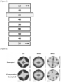
- FIGS. 2 , 5 , 8 , and 9 The structure of the liquid crystal display schematically illustrated in FIGS. 2 , 5 , 8 , and 9 below. More specifically according to the claimed invention, FIG 2 below illustrates a liquid crystal display comprising two quarter wave plates as the wave plate and FIG 5 below illustrates a liquid crystal display comprising four quarter wave plates as the wave plate. In addition and not according to the claimed invention, FIG. 8 below illustrates a liquid crystal display comprising one half wave plate as the wave plate and FIG 9 below illustrates a liquid crystal display comprising two half wave plates as the wave plate.
- a mass-produced polarizer (made by LG Chemical Co., Ltd.) which is laminated in a structure of TAC/PVA/TAC was cut so that the absorption axis becomes 0 degree and used as a base substrate and two quarter wave plates (144 nm, made by Fuji Film) having an optical axis of 22.5 degrees are joined to the cut polarizer by using the gluing agent. Thereafter, the same quarter wave plate fabric was cut to have an optical axis of 67.5 degrees and then, two additional sheets were attached to the lower portion of a half wave plate which was previously attached to the bonding product by using the gluing agent. Thereafter, a polarization plate was fabricated by applying the gluing agent to the lower portion of the half wave plate having the optical axis of 67.5 degrees.
- the polarization plate was attached to the upper portion of the liquid crystal panel and a general polarizer used as the base substrate was attached to the lower portion of the liquid crystal panel with an absorption axis of 0 degree.
- a polarization plate comprising the half wave plate was fabricated by the same method as Example 1, the fabricated polarization plate was attached to the lower portion of the liquid crystal panel with the absorption axis of 0 degree, and the general polarizer used as the base substrate was attached to the upper portion of the liquid crystal panel with the absorption axis of 0 degree.
- Comparative Example 1 which is not according to the claimed invention, is schematically illustrated in FIG 6 below.
- a general polarizer which is laminated in a structure of TAC/PVA/TAC was cut so that the absorption axis becomes 0 degree and used as the base substrate and two quarter wave plates (144 nm, made by Fuji Film) having the optical axis of 45 degrees are joined to the cut polarizer by using the gluing agent. Thereafter, the polarization plate was fabricated by applying the gluing agent to the lower portion of the half wave plate which was previously attached.
- the polarization plate was attached to the upper portion of the liquid crystal panel and a general polarizer used as the base substrate was attached to the lower portion of the liquid crystal panel with an absorption axis of 0 degree.
- Example 2 The structure of Example 2, which is according to the claimed invention, is schematically illustrated in FIG 2 below.
- the polarization plate comprising the half wave plate was fabricated by the same method as Example 2, the fabricated polarization plate was attached to the lower portion of the liquid crystal panel with the absorption axis of 0 degree, and the general polarizer used as the base substrate was attached to the upper portion of the liquid crystal panel with the absorption axis of 0 degree.
- Comparative Example 2 which is not according to the claimed invention, is schematically illustrated in FIG 3 below.
- Optical characteristics of the polarization plate attached to the panel according to Examples 1 and 2 and Comparative Examples 1 and 2 were measured and shown in Tables 1, 4, and 7 below.
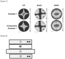
- FIG 4 below illustrates results depending on Example 2 and Comparative Example 2
- FIG 7 illustrates results depending on Example 1 and Comparative Example 1.
- the optical characteristics were measured and compared at the same position of the same panel.
- a panel used for evaluation is a 12.3" product of IPS mode and black luminance and white luminance were measured b using EZ contrast 160R made by Eldim as an optical measurer and relatively compared with the comparative example.
- EZ contrast 160R made by Eldim as an optical measurer
- C/R represents a contrast ratio representing a white luminance/black luminance value
- the data shows a relative ratio of luminance values in black and white at the front having an azimuth angle of 0 degree and a polar angle of 0 degree.
- the C/R value of Example 1 having +54% means that the C/R value increases as compared with Comparative Example 1 by 54% and +59% of Example 2 means that the C/R value increases as compared with Comparative Example 2 by 59%.
- the C/R increases by approximately 50% or more as compared with a case where the polarization plate is positioned at the lower portion of the panel.
- Example 3 is configured by setting the absorption axis of the upper polarizer to 0 degree and sequentially laminating two quarter wave plates on the lower portion, which have the optical axis of 67.5 degrees, and sequentially laminating two quarter wave plates on the lower portion, which have the optical axis of 22.5 degrees.
- R(450)/R(550) of the applied quarter wave plate is 0.86
- R(450) means retardation at 450 nm
- R (550) means retardation at 550 nm.
- the Example is configured by locating the structure of the polarization plate at the upper portion of the liquid crystal layer and setting the absorption axis of the polarizer to 0 degree at the lower portion.
- Example 3 which is according to the claimed invention, is schematically illustrated in FIG 10 below.
- Example 4 is configured by setting the absorption axis of the upper polarizer to 0 degree and sequentially laminating two quarter wave plates on the lower portion, which have the optical axis of 22.5 degrees, and sequentially laminating two quarter wave plates on the lower portion, which have the optical axis of 67.5 degrees.
- R(450)/R(550) of the applied quarter wave plate is 0.86
- R(450) means retardation at 450 nm
- R (550) means retardation at 550 nm.
- Example 4 is configured by locating the structure of the polarization plate at the upper portion of the liquid crystal layer and setting the absorption axis of the polarizer to 0 degree at the lower portion.
- Example 4 which is according to the claimed invention, is schematically illustrated in FIG 10 below.
- the absorption axis of the upper polarizer is set to 0, and one half wave plate having an optical axis of 79 degrees, one half wave plate having an optical axis of 45 degrees, and one half wave plate having an optical axis of 11 degrees are sequentially laminated at the lower portion.
- R(450)/R(550) of the applied half wave plate is 0.86
- R(450) means retardation at 450 nm
- R (550) means retardation at 550 nm.
- Comparative Example 3 is configured by locating the structure of the polarization plate at the upper portion of the liquid crystal layer and setting the absorption axis of the polarizer to 0 degree at the lower portion.
- Comparative Example 3 which is not according to the claimed invention, is schematically illustrated in FIG 11 below.
- the front black luminance means luminance at the azimuth angle of 0 degree and the polar angle of 0 degree
- the viewing angle black max means a value of a portion with highest black luminance at a front azimuth angle and a front azimuth angle.
- the wave plate when the wave plate is provided between the upper polarizer and the liquid crystal panel, which rotates the linearly polarized light at 85 to 95 degrees, the wave plate comprises four quarter wave plates, and angles formed between the optical axes of any two quarter wave plates among the four quarter wave plates and the absorption axis of the upper polarizer is in the range of 20 degrees to 25 degrees and angles formed between the optical axes of the other two quarter wave plates and the absorption axis of the upper polarizer is in the range of 65 degrees to 70 degrees, the front contrast ratio (CR) may be more effectively increased by effectively rotating the polarization as compared with a case of configuring a polarization rotation layer in a range which is out of the angle.
- the front contrast ratio CR
Landscapes
- Physics & Mathematics (AREA)
- Nonlinear Science (AREA)
- Chemical & Material Sciences (AREA)
- Mathematical Physics (AREA)
- Crystallography & Structural Chemistry (AREA)
- General Physics & Mathematics (AREA)
- Optics & Photonics (AREA)
- Geometry (AREA)
- Dispersion Chemistry (AREA)
- Polarising Elements (AREA)
- Liquid Crystal (AREA)
Claims (7)
- Afficheur à cristaux liquides comprenant :un polariseur supérieur (10) ;un polariseur inférieur (20) ; etun panneau à cristaux liquides (30) fourni entre le polariseur supérieur (10) et le polariseur inférieur (20),dans lequel le polariseur supérieur (10) et le polariseur inférieur (20) sont fournis de telle sorte que leurs axes d'absorption sont parallèles l'un à l'autre,une plaque d'onde (50) est fournie entre le polariseur supérieur (10) et le panneau à cristaux liquides (30), la plaque d'onde (50) étant configurée pour faire tourner la lumière polarisée linéairement de 85 à 95 degrés, etle panneau à cristaux liquides (30) est configuré pour être dans un mode à cristaux liquides à alignement horizontal,dans lequel la plaque d'onde (50) comprend deux ou quatre plaques quart d'onde (50),dans lequel le polariseur inférieur (20) est fixé à une partie inférieure du panneau à cristaux liquides (30) et entre le panneau à cristaux liquides (30) et une unité de rétroéclairage, et le polariseur supérieur (10) est fixé à une partie supérieure du panneau à cristaux liquides (30) opposée à la partie inférieure.
- Afficheur à cristaux liquides selon la revendication 1, dans lequel la plaque d'onde (50) comprend deux plaques quart d'onde (50), et
des angles entre les axes optiques des deux plaques quart d'onde (50) et l'axe d'absorption du polariseur supérieur (10) sont dans la plage de 40 à 50 degrés ou de 130 à 140 degrés. - Afficheur à cristaux liquides selon la revendication 1, dans lequel la plaque d'onde (50) comprend quatre plaques quart d'onde (50), et
des angles formés entre l'axe optique de l'une des deux plaques quart d'onde (50) parmi les quatre plaques quart d'onde (50) et l'axe d'absorption du polariseur supérieur (10) sont dans la plage de 20 degrés à 25 degrés et des angles formés entre les axes optiques des autres deux plaques quart d'onde (50) et l'axe d'absorption du polariseur supérieur (10) sont dans la plage de 65 degrés à 70 degrés. - Afficheur à cristaux liquides selon la revendication 1, comprenant en outre :
un film de compensation d'angle de visualisation entre la plaque d'onde (50) et le panneau à cristaux liquides (30). - Afficheur à cristaux liquides selon la revendication 1, comprenant en outre :
un film de compensation d'angle de visualisation entre la plaque d'onde (50) et le polariseur supérieur (10). - Afficheur à cristaux liquides selon la revendication 1, dans lequel le polariseur supérieur (10) et le polariseur inférieur (20) sont chacun et individuellement un polariseur d'alcool polyvinylique dans lequel soit un colorant iodé, soit un colorant dichroïque, est coloré.
- Afficheur à cristaux liquides selon la revendication 1, dans lequel le panneau à cristaux liquides (30) est un panneau à cristaux liquides en mode commutation dans le plan (In Plane Switching, IPS) ou un panneau à cristaux liquides en mode commutation de plan à ligne (Plane to Line Switching, PLS).
Applications Claiming Priority (2)
| Application Number | Priority Date | Filing Date | Title |
|---|---|---|---|
| KR20180001110 | 2018-01-04 | ||
| PCT/KR2018/016628 WO2019135535A1 (fr) | 2018-01-04 | 2018-12-26 | Dispositif d'affichage à cristaux liquides et procédé de fabrication associé |
Publications (3)
| Publication Number | Publication Date |
|---|---|
| EP3736621A1 EP3736621A1 (fr) | 2020-11-11 |
| EP3736621A4 EP3736621A4 (fr) | 2020-12-09 |
| EP3736621B1 true EP3736621B1 (fr) | 2024-12-11 |
Family
ID=67143913
Family Applications (1)
| Application Number | Title | Priority Date | Filing Date |
|---|---|---|---|
| EP18898754.9A Active EP3736621B1 (fr) | 2018-01-04 | 2018-12-26 | Dispositif d'affichage à cristaux liquides |
Country Status (7)
| Country | Link |
|---|---|
| US (1) | US11428990B2 (fr) |
| EP (1) | EP3736621B1 (fr) |
| JP (1) | JP2020529627A (fr) |
| KR (1) | KR102104727B1 (fr) |
| CN (1) | CN111033370B (fr) |
| TW (1) | TWI728296B (fr) |
| WO (1) | WO2019135535A1 (fr) |
Families Citing this family (5)
| Publication number | Priority date | Publication date | Assignee | Title |
|---|---|---|---|---|
| CN112684627B (zh) | 2020-12-30 | 2023-03-07 | 天马微电子股份有限公司 | 液晶显示面板及显示装置 |
| CN112698527B (zh) | 2020-12-30 | 2023-04-18 | 天马微电子股份有限公司 | 液晶显示面板及显示装置 |
| CN113219711A (zh) * | 2021-04-25 | 2021-08-06 | 北海惠科光电技术有限公司 | 显示面板和显示装置 |
| WO2023149359A1 (fr) * | 2022-02-04 | 2023-08-10 | 富士フイルム株式会社 | Stratifié optique et dispositif d'affichage d'image |
| CN115185123B (zh) * | 2022-07-15 | 2023-08-22 | Tcl华星光电技术有限公司 | 液晶显示屏 |
Family Cites Families (16)
| Publication number | Priority date | Publication date | Assignee | Title |
|---|---|---|---|---|
| WO2004081640A1 (fr) | 1996-10-30 | 2004-09-23 | Toshiaki Hashizume | Afficheur a projection |
| JP3972927B2 (ja) * | 1996-10-30 | 2007-09-05 | セイコーエプソン株式会社 | 投写型表示装置 |
| US20030016325A1 (en) | 2001-07-23 | 2003-01-23 | Nec Corporation | Liquid crystal display device |
| JP3823972B2 (ja) | 2003-05-09 | 2006-09-20 | セイコーエプソン株式会社 | 視角制御素子、表示装置、及び電子機器 |
| JP4470904B2 (ja) * | 2003-05-09 | 2010-06-02 | セイコーエプソン株式会社 | 視角制御素子、表示装置、及び電子機器 |
| KR20070082768A (ko) * | 2006-02-17 | 2007-08-22 | 삼성전자주식회사 | 액정표시장치 |
| JP4822432B2 (ja) * | 2006-07-25 | 2011-11-24 | 日東電工株式会社 | 液晶パネル、及び液晶表示装置 |
| US8045097B2 (en) | 2006-08-09 | 2011-10-25 | Sharp Kabushiki Kaisha | Liquid crystal display device and viewing angle control module |
| CN103197464B (zh) | 2013-03-29 | 2015-10-21 | 深圳市华星光电技术有限公司 | 液晶显示面板及液晶显示器 |
| KR20150007518A (ko) * | 2013-07-11 | 2015-01-21 | 동우 화인켐 주식회사 | 액정 패널 및 이를 구비하는 액정 표시 장치 |
| KR101589347B1 (ko) * | 2013-07-31 | 2016-01-27 | 제일모직주식회사 | 액정표시장치용 모듈 및 이를 포함하는 액정표시장치 |
| JP6274971B2 (ja) | 2014-05-26 | 2018-02-07 | 株式会社Nttドコモ | ヘッドマウントディスプレイ |
| KR101790404B1 (ko) | 2015-02-25 | 2017-10-26 | 주식회사 엘지화학 | 편광자의 제조방법, 이를 이용하여 제조된 편광자, 이를 포함하는 편광판 및 화상표시장치 |
| KR20160112380A (ko) * | 2015-03-19 | 2016-09-28 | 동우 화인켐 주식회사 | 액정 패널 및 이를 구비하는 액정 표시 장치 |
| US9933631B2 (en) * | 2016-03-28 | 2018-04-03 | Lc-Tec Displays Ab | Electro-optic guest-host liquid crystal variable transmission filter with wide viewing angle |
| KR20180001110A (ko) | 2016-06-27 | 2018-01-04 | 주식회사 지케이에스 | 꾸지뽕나무, 세신, 속단, 마가목 추출물을 기반으로 하는 주름개선, 피부미백, 피부항산화 기능성 천연복합 화장품 조성물 |
-
2018
- 2018-12-26 EP EP18898754.9A patent/EP3736621B1/fr active Active
- 2018-12-26 WO PCT/KR2018/016628 patent/WO2019135535A1/fr not_active Ceased
- 2018-12-26 US US16/633,747 patent/US11428990B2/en active Active
- 2018-12-26 CN CN201880051453.3A patent/CN111033370B/zh active Active
- 2018-12-26 JP JP2020505222A patent/JP2020529627A/ja active Pending
- 2018-12-26 KR KR1020180169341A patent/KR102104727B1/ko active Active
-
2019
- 2019-01-02 TW TW108100049A patent/TWI728296B/zh active
Also Published As
| Publication number | Publication date |
|---|---|
| TWI728296B (zh) | 2021-05-21 |
| EP3736621A4 (fr) | 2020-12-09 |
| EP3736621A1 (fr) | 2020-11-11 |
| CN111033370B (zh) | 2023-04-07 |
| JP2020529627A (ja) | 2020-10-08 |
| US20210088854A1 (en) | 2021-03-25 |
| TW201937255A (zh) | 2019-09-16 |
| KR20190083614A (ko) | 2019-07-12 |
| KR102104727B1 (ko) | 2020-04-24 |
| CN111033370A (zh) | 2020-04-17 |
| US11428990B2 (en) | 2022-08-30 |
| WO2019135535A1 (fr) | 2019-07-11 |
Similar Documents
| Publication | Publication Date | Title |
|---|---|---|
| EP3677958B1 (fr) | Empilement et dispositif d'affichage à cristaux liquides comprenant ce dernier | |
| EP3677957B1 (fr) | Dispositif d'affichage à cristaux liquides | |
| US11275266B2 (en) | Laminate and liquid crystal display device comprising same | |
| US11428990B2 (en) | Liquid crystal display device and manufacturing method thereof | |
| EP3805853B1 (fr) | Stratifié et dispositif d'affichage à cristaux liquides le comprenant |
Legal Events
| Date | Code | Title | Description |
|---|---|---|---|
| STAA | Information on the status of an ep patent application or granted ep patent |
Free format text: STATUS: THE INTERNATIONAL PUBLICATION HAS BEEN MADE |
|
| PUAI | Public reference made under article 153(3) epc to a published international application that has entered the european phase |
Free format text: ORIGINAL CODE: 0009012 |
|
| STAA | Information on the status of an ep patent application or granted ep patent |
Free format text: STATUS: REQUEST FOR EXAMINATION WAS MADE |
|
| REG | Reference to a national code |
Ref country code: DE Ref legal event code: R079 Free format text: PREVIOUS MAIN CLASS: G02F0001133500 Ipc: G02F0001133630 Ref country code: DE Ref legal event code: R079 Ref document number: 602018077605 Country of ref document: DE Free format text: PREVIOUS MAIN CLASS: G02F0001133500 Ipc: G02F0001133630 |
|
| 17P | Request for examination filed |
Effective date: 20200122 |
|
| AK | Designated contracting states |
Kind code of ref document: A1 Designated state(s): AL AT BE BG CH CY CZ DE DK EE ES FI FR GB GR HR HU IE IS IT LI LT LU LV MC MK MT NL NO PL PT RO RS SE SI SK SM TR |
|
| AX | Request for extension of the european patent |
Extension state: BA ME |
|
| A4 | Supplementary search report drawn up and despatched |
Effective date: 20201109 |
|
| RIC1 | Information provided on ipc code assigned before grant |
Ipc: G02F 1/1335 20060101ALI20201103BHEP Ipc: G02F 1/13363 20060101AFI20201103BHEP Ipc: G02F 1/1343 20060101ALI20201103BHEP |
|
| DAV | Request for validation of the european patent (deleted) | ||
| DAX | Request for extension of the european patent (deleted) | ||
| STAA | Information on the status of an ep patent application or granted ep patent |
Free format text: STATUS: EXAMINATION IS IN PROGRESS |
|
| 17Q | First examination report despatched |
Effective date: 20220920 |
|
| GRAP | Despatch of communication of intention to grant a patent |
Free format text: ORIGINAL CODE: EPIDOSNIGR1 |
|
| STAA | Information on the status of an ep patent application or granted ep patent |
Free format text: STATUS: GRANT OF PATENT IS INTENDED |
|
| GRAS | Grant fee paid |
Free format text: ORIGINAL CODE: EPIDOSNIGR3 |
|
| INTG | Intention to grant announced |
Effective date: 20241002 |
|
| GRAA | (expected) grant |
Free format text: ORIGINAL CODE: 0009210 |
|
| STAA | Information on the status of an ep patent application or granted ep patent |
Free format text: STATUS: THE PATENT HAS BEEN GRANTED |
|
| AK | Designated contracting states |
Kind code of ref document: B1 Designated state(s): AL AT BE BG CH CY CZ DE DK EE ES FI FR GB GR HR HU IE IS IT LI LT LU LV MC MK MT NL NO PL PT RO RS SE SI SK SM TR |
|
| REG | Reference to a national code |
Ref country code: GB Ref legal event code: FG4D |
|
| REG | Reference to a national code |
Ref country code: CH Ref legal event code: EP |
|
| REG | Reference to a national code |
Ref country code: IE Ref legal event code: FG4D |
|
| REG | Reference to a national code |
Ref country code: DE Ref legal event code: R096 Ref document number: 602018077605 Country of ref document: DE |
|
| PGFP | Annual fee paid to national office [announced via postgrant information from national office to epo] |
Ref country code: DE Payment date: 20241223 Year of fee payment: 7 |
|
| PGFP | Annual fee paid to national office [announced via postgrant information from national office to epo] |
Ref country code: GB Payment date: 20241223 Year of fee payment: 7 |
|
| PGFP | Annual fee paid to national office [announced via postgrant information from national office to epo] |
Ref country code: FR Payment date: 20241224 Year of fee payment: 7 |
|
| REG | Reference to a national code |
Ref country code: LT Ref legal event code: MG9D |
|
| PG25 | Lapsed in a contracting state [announced via postgrant information from national office to epo] |
Ref country code: HR Free format text: LAPSE BECAUSE OF FAILURE TO SUBMIT A TRANSLATION OF THE DESCRIPTION OR TO PAY THE FEE WITHIN THE PRESCRIBED TIME-LIMIT Effective date: 20241211 |
|
| PG25 | Lapsed in a contracting state [announced via postgrant information from national office to epo] |
Ref country code: FI Free format text: LAPSE BECAUSE OF FAILURE TO SUBMIT A TRANSLATION OF THE DESCRIPTION OR TO PAY THE FEE WITHIN THE PRESCRIBED TIME-LIMIT Effective date: 20241211 |
|
| PG25 | Lapsed in a contracting state [announced via postgrant information from national office to epo] |
Ref country code: BG Free format text: LAPSE BECAUSE OF FAILURE TO SUBMIT A TRANSLATION OF THE DESCRIPTION OR TO PAY THE FEE WITHIN THE PRESCRIBED TIME-LIMIT Effective date: 20241211 |
|
| REG | Reference to a national code |
Ref country code: NL Ref legal event code: MP Effective date: 20241211 |
|
| PG25 | Lapsed in a contracting state [announced via postgrant information from national office to epo] |
Ref country code: ES Free format text: LAPSE BECAUSE OF FAILURE TO SUBMIT A TRANSLATION OF THE DESCRIPTION OR TO PAY THE FEE WITHIN THE PRESCRIBED TIME-LIMIT Effective date: 20241211 |
|
| PG25 | Lapsed in a contracting state [announced via postgrant information from national office to epo] |
Ref country code: NO Free format text: LAPSE BECAUSE OF FAILURE TO SUBMIT A TRANSLATION OF THE DESCRIPTION OR TO PAY THE FEE WITHIN THE PRESCRIBED TIME-LIMIT Effective date: 20250311 |
|
| PG25 | Lapsed in a contracting state [announced via postgrant information from national office to epo] |
Ref country code: LV Free format text: LAPSE BECAUSE OF FAILURE TO SUBMIT A TRANSLATION OF THE DESCRIPTION OR TO PAY THE FEE WITHIN THE PRESCRIBED TIME-LIMIT Effective date: 20241211 Ref country code: GR Free format text: LAPSE BECAUSE OF FAILURE TO SUBMIT A TRANSLATION OF THE DESCRIPTION OR TO PAY THE FEE WITHIN THE PRESCRIBED TIME-LIMIT Effective date: 20250312 |
|
| PG25 | Lapsed in a contracting state [announced via postgrant information from national office to epo] |
Ref country code: RS Free format text: LAPSE BECAUSE OF FAILURE TO SUBMIT A TRANSLATION OF THE DESCRIPTION OR TO PAY THE FEE WITHIN THE PRESCRIBED TIME-LIMIT Effective date: 20250311 |
|
| PG25 | Lapsed in a contracting state [announced via postgrant information from national office to epo] |
Ref country code: NL Free format text: LAPSE BECAUSE OF FAILURE TO SUBMIT A TRANSLATION OF THE DESCRIPTION OR TO PAY THE FEE WITHIN THE PRESCRIBED TIME-LIMIT Effective date: 20241211 |
|
| REG | Reference to a national code |
Ref country code: AT Ref legal event code: MK05 Ref document number: 1750860 Country of ref document: AT Kind code of ref document: T Effective date: 20241211 |
|
| PG25 | Lapsed in a contracting state [announced via postgrant information from national office to epo] |
Ref country code: SM Free format text: LAPSE BECAUSE OF FAILURE TO SUBMIT A TRANSLATION OF THE DESCRIPTION OR TO PAY THE FEE WITHIN THE PRESCRIBED TIME-LIMIT Effective date: 20241211 |
|
| PG25 | Lapsed in a contracting state [announced via postgrant information from national office to epo] |
Ref country code: PL Free format text: LAPSE BECAUSE OF FAILURE TO SUBMIT A TRANSLATION OF THE DESCRIPTION OR TO PAY THE FEE WITHIN THE PRESCRIBED TIME-LIMIT Effective date: 20241211 |
|
| PG25 | Lapsed in a contracting state [announced via postgrant information from national office to epo] |
Ref country code: IS Free format text: LAPSE BECAUSE OF FAILURE TO SUBMIT A TRANSLATION OF THE DESCRIPTION OR TO PAY THE FEE WITHIN THE PRESCRIBED TIME-LIMIT Effective date: 20250411 |
|
| PG25 | Lapsed in a contracting state [announced via postgrant information from national office to epo] |
Ref country code: PT Free format text: LAPSE BECAUSE OF FAILURE TO SUBMIT A TRANSLATION OF THE DESCRIPTION OR TO PAY THE FEE WITHIN THE PRESCRIBED TIME-LIMIT Effective date: 20250411 |
|
| PG25 | Lapsed in a contracting state [announced via postgrant information from national office to epo] |
Ref country code: EE Free format text: LAPSE BECAUSE OF FAILURE TO SUBMIT A TRANSLATION OF THE DESCRIPTION OR TO PAY THE FEE WITHIN THE PRESCRIBED TIME-LIMIT Effective date: 20241211 |
|
| PG25 | Lapsed in a contracting state [announced via postgrant information from national office to epo] |
Ref country code: AT Free format text: LAPSE BECAUSE OF FAILURE TO SUBMIT A TRANSLATION OF THE DESCRIPTION OR TO PAY THE FEE WITHIN THE PRESCRIBED TIME-LIMIT Effective date: 20241211 Ref country code: RO Free format text: LAPSE BECAUSE OF FAILURE TO SUBMIT A TRANSLATION OF THE DESCRIPTION OR TO PAY THE FEE WITHIN THE PRESCRIBED TIME-LIMIT Effective date: 20241211 |
|
| PG25 | Lapsed in a contracting state [announced via postgrant information from national office to epo] |
Ref country code: SK Free format text: LAPSE BECAUSE OF FAILURE TO SUBMIT A TRANSLATION OF THE DESCRIPTION OR TO PAY THE FEE WITHIN THE PRESCRIBED TIME-LIMIT Effective date: 20241211 |
|
| PG25 | Lapsed in a contracting state [announced via postgrant information from national office to epo] |
Ref country code: CZ Free format text: LAPSE BECAUSE OF FAILURE TO SUBMIT A TRANSLATION OF THE DESCRIPTION OR TO PAY THE FEE WITHIN THE PRESCRIBED TIME-LIMIT Effective date: 20241211 |
|
| PG25 | Lapsed in a contracting state [announced via postgrant information from national office to epo] |
Ref country code: IT Free format text: LAPSE BECAUSE OF FAILURE TO SUBMIT A TRANSLATION OF THE DESCRIPTION OR TO PAY THE FEE WITHIN THE PRESCRIBED TIME-LIMIT Effective date: 20241211 |
|
| REG | Reference to a national code |
Ref country code: CH Ref legal event code: PL |
|
| PG25 | Lapsed in a contracting state [announced via postgrant information from national office to epo] |
Ref country code: LU Free format text: LAPSE BECAUSE OF NON-PAYMENT OF DUE FEES Effective date: 20241226 |
|
| PG25 | Lapsed in a contracting state [announced via postgrant information from national office to epo] |
Ref country code: SE Free format text: LAPSE BECAUSE OF FAILURE TO SUBMIT A TRANSLATION OF THE DESCRIPTION OR TO PAY THE FEE WITHIN THE PRESCRIBED TIME-LIMIT Effective date: 20241211 |
|
| REG | Reference to a national code |
Ref country code: DE Ref legal event code: R097 Ref document number: 602018077605 Country of ref document: DE |
|
| PG25 | Lapsed in a contracting state [announced via postgrant information from national office to epo] |
Ref country code: MC Free format text: LAPSE BECAUSE OF FAILURE TO SUBMIT A TRANSLATION OF THE DESCRIPTION OR TO PAY THE FEE WITHIN THE PRESCRIBED TIME-LIMIT Effective date: 20241211 |
|
| REG | Reference to a national code |
Ref country code: BE Ref legal event code: MM Effective date: 20241231 |
|
| PG25 | Lapsed in a contracting state [announced via postgrant information from national office to epo] |
Ref country code: DK Free format text: LAPSE BECAUSE OF FAILURE TO SUBMIT A TRANSLATION OF THE DESCRIPTION OR TO PAY THE FEE WITHIN THE PRESCRIBED TIME-LIMIT Effective date: 20241211 |
|
| PG25 | Lapsed in a contracting state [announced via postgrant information from national office to epo] |
Ref country code: BE Free format text: LAPSE BECAUSE OF NON-PAYMENT OF DUE FEES Effective date: 20241231 |
|
| PLBE | No opposition filed within time limit |
Free format text: ORIGINAL CODE: 0009261 |
|
| STAA | Information on the status of an ep patent application or granted ep patent |
Free format text: STATUS: NO OPPOSITION FILED WITHIN TIME LIMIT |
|
| PG25 | Lapsed in a contracting state [announced via postgrant information from national office to epo] |
Ref country code: CH Free format text: LAPSE BECAUSE OF NON-PAYMENT OF DUE FEES Effective date: 20241231 |
|
| PG25 | Lapsed in a contracting state [announced via postgrant information from national office to epo] |
Ref country code: IE Free format text: LAPSE BECAUSE OF NON-PAYMENT OF DUE FEES Effective date: 20241226 |
|
| 26N | No opposition filed |
Effective date: 20250912 |
|
| PG25 | Lapsed in a contracting state [announced via postgrant information from national office to epo] |
Ref country code: CY Free format text: LAPSE BECAUSE OF FAILURE TO SUBMIT A TRANSLATION OF THE DESCRIPTION OR TO PAY THE FEE WITHIN THE PRESCRIBED TIME-LIMIT Effective date: 20241211 |
|
| PG25 | Lapsed in a contracting state [announced via postgrant information from national office to epo] |
Ref country code: TR Free format text: LAPSE BECAUSE OF FAILURE TO SUBMIT A TRANSLATION OF THE DESCRIPTION OR TO PAY THE FEE WITHIN THE PRESCRIBED TIME-LIMIT Effective date: 20241211 |
|
| PG25 | Lapsed in a contracting state [announced via postgrant information from national office to epo] |
Ref country code: HU Free format text: LAPSE BECAUSE OF FAILURE TO SUBMIT A TRANSLATION OF THE DESCRIPTION OR TO PAY THE FEE WITHIN THE PRESCRIBED TIME-LIMIT; INVALID AB INITIO Effective date: 20181226 |
|
| PG25 | Lapsed in a contracting state [announced via postgrant information from national office to epo] |
Ref country code: SI Free format text: LAPSE BECAUSE OF FAILURE TO SUBMIT A TRANSLATION OF THE DESCRIPTION OR TO PAY THE FEE WITHIN THE PRESCRIBED TIME-LIMIT Effective date: 20241211 |
|
| PG25 | Lapsed in a contracting state [announced via postgrant information from national office to epo] |
Ref country code: LT Free format text: LAPSE BECAUSE OF FAILURE TO SUBMIT A TRANSLATION OF THE DESCRIPTION OR TO PAY THE FEE WITHIN THE PRESCRIBED TIME-LIMIT Effective date: 20241211 |