EP3680908A1 - Dispositif de limitation d'une dissipation de puissance lors du balayage d'un signal numérique - Google Patents
Dispositif de limitation d'une dissipation de puissance lors du balayage d'un signal numérique Download PDFInfo
- Publication number
- EP3680908A1 EP3680908A1 EP19217537.0A EP19217537A EP3680908A1 EP 3680908 A1 EP3680908 A1 EP 3680908A1 EP 19217537 A EP19217537 A EP 19217537A EP 3680908 A1 EP3680908 A1 EP 3680908A1
- Authority
- EP
- European Patent Office
- Prior art keywords
- sample
- current
- sampling
- pause
- signal
- Prior art date
- Legal status (The legal status is an assumption and is not a legal conclusion. Google has not performed a legal analysis and makes no representation as to the accuracy of the status listed.)
- Granted
Links
Images




Classifications
-
- G—PHYSICS
- G11—INFORMATION STORAGE
- G11C—STATIC STORES
- G11C27/00—Electric analogue stores, e.g. for storing instantaneous values
- G11C27/02—Sample-and-hold arrangements
- G11C27/024—Sample-and-hold arrangements using a capacitive memory element
- G11C27/028—Current mode circuits, e.g. switched current memories
-
- H—ELECTRICITY
- H02—GENERATION; CONVERSION OR DISTRIBUTION OF ELECTRIC POWER
- H02M—APPARATUS FOR CONVERSION BETWEEN AC AND AC, BETWEEN AC AND DC, OR BETWEEN DC AND DC, AND FOR USE WITH MAINS OR SIMILAR POWER SUPPLY SYSTEMS; CONVERSION OF DC OR AC INPUT POWER INTO SURGE OUTPUT POWER; CONTROL OR REGULATION THEREOF
- H02M3/00—Conversion of DC power input into DC power output
- H02M3/02—Conversion of DC power input into DC power output without intermediate conversion into AC
- H02M3/04—Conversion of DC power input into DC power output without intermediate conversion into AC by static converters
- H02M3/10—Conversion of DC power input into DC power output without intermediate conversion into AC by static converters using discharge tubes with control electrode or semiconductor devices with control electrode
- H02M3/145—Conversion of DC power input into DC power output without intermediate conversion into AC by static converters using discharge tubes with control electrode or semiconductor devices with control electrode using devices of a triode or transistor type requiring continuous application of a control signal
- H02M3/155—Conversion of DC power input into DC power output without intermediate conversion into AC by static converters using discharge tubes with control electrode or semiconductor devices with control electrode using devices of a triode or transistor type requiring continuous application of a control signal using semiconductor devices only
- H02M3/156—Conversion of DC power input into DC power output without intermediate conversion into AC by static converters using discharge tubes with control electrode or semiconductor devices with control electrode using devices of a triode or transistor type requiring continuous application of a control signal using semiconductor devices only with automatic control of output voltage or current, e.g. switching regulators
- H02M3/157—Conversion of DC power input into DC power output without intermediate conversion into AC by static converters using discharge tubes with control electrode or semiconductor devices with control electrode using devices of a triode or transistor type requiring continuous application of a control signal using semiconductor devices only with automatic control of output voltage or current, e.g. switching regulators with digital control
-
- G—PHYSICS
- G05—CONTROLLING; REGULATING
- G05F—SYSTEMS FOR REGULATING ELECTRIC OR MAGNETIC VARIABLES
- G05F3/00—Non-retroactive systems for regulating electric variables by using an uncontrolled element, or an uncontrolled combination of elements, such element or such combination having self-regulating properties
- G05F3/02—Regulating voltage or current
- G05F3/08—Regulating voltage or current wherein the variable is DC
- G05F3/10—Regulating voltage or current wherein the variable is DC using uncontrolled devices with non-linear characteristics
- G05F3/16—Regulating voltage or current wherein the variable is DC using uncontrolled devices with non-linear characteristics being semiconductor devices
- G05F3/20—Regulating voltage or current wherein the variable is DC using uncontrolled devices with non-linear characteristics being semiconductor devices using diode- transistor combinations
- G05F3/26—Current mirrors
- G05F3/262—Current mirrors using field-effect transistors only
-
- H—ELECTRICITY
- H03—ELECTRONIC CIRCUITRY
- H03K—PULSE TECHNIQUE
- H03K17/00—Electronic switching or gating, i.e. not by contact-making and –breaking
- H03K17/51—Electronic switching or gating, i.e. not by contact-making and –breaking characterised by the components used
- H03K17/56—Electronic switching or gating, i.e. not by contact-making and –breaking characterised by the components used by the use, as active elements, of semiconductor devices
- H03K17/60—Electronic switching or gating, i.e. not by contact-making and –breaking characterised by the components used by the use, as active elements, of semiconductor devices the devices being bipolar transistors
Definitions
- the present invention relates to a device for limiting a power loss when sampling a digital signal.
- the voltage or the current representing the digital signal is measured at specific points in time and assigned to a signal value representing a range of values, for example a high level or a low level.
- the invention enriches the prior art, as devices according to the invention reduce the power loss when sampling a digital signal, by reducing the current flow along the signal path during sampling pauses.
- a device for this purpose, comprises a circuit arranged in the signal path of the digital signal, the circuit being set up to reduce a current flow along the signal path in response to a control signal which indicates a sampling pause.
- signal path includes, in particular, an electrically conductive connection (during scanning) between a circuit (transmitter) generating the digital signal and a circuit (receiver) receiving the digital signal.
- the circuit can be connected upstream of a digital input and only "pass through” the digital signal if the signal present at the input is actually is read.
- the signal at the input can be read in cyclically (for example, controlled by a timer), so that there are (sampling) pauses during the reading times in which the signal is not read.
- control signal as used in the description and the claims is to be understood in particular as an electrical signal which, for example, controls an electronic component (for example a transistor), by means of which the circuit is switched from a first Mode in which the digital signal is (essentially) "passed through” can be switched to a second mode in which the current flow to the input is reduced.
- the control signal can have a first voltage, for example, during the (sampling) pauses and a second voltage (which is, for example, greater than the first voltage) at read-in times.
- sampling is to be understood in particular as measuring and assigning a digital signal to a signal value.
- sampling pause as used in the description and the claims is to be understood in particular to mean a period of time during which no measurement and assignment of a digital signal to a signal value is carried out, or during which an assignment is not made continues to be used (ie ignored and continuously overwritten).
- the circuit preferably has a current limiting circuit and the current limiting circuit is varied by a switching element which is controlled by the control signal.
- the current limiting circuit preferably has an input resistance, the current flow through the current limiting circuit being limited by the input resistance to reduce the power loss.
- the digital signal preferably comprises current / voltage levels in a lower current / voltage level range and an upper current / voltage level range.
- the device is designed to generate the control signal which indicates a sampling pause when a sample lies in the upper current / voltage level range and not to generate the control signal which indicates a sampling pause when a sample lies in the lower current / voltage level range .
- the apparatus is arranged to sample the digital signal at certain times, to acquire a sample and to generate the control signal which indicates a sampling pause when the sample is in the upper current / voltage level range, the current / voltage level of the digital signal during the sampling pause along the signal path to limit the power loss is reduced by the device.
- the current level of the digital signal is preferably reduced during the sampling pause along the signal path in order to limit the power loss by the device.
- the device preferably further comprises a microcontroller and a storage element and is set up to store a sample in the storage element in response to a request signal from the microcontroller and to display a sampling pause after the storage until the microcontroller generates a next request signal.
- the device is preferably set up to generate the control signal, which indicates a sampling pause, when a sampling pause is displayed and the sample value stored in the memory element corresponds to a high level.
- the device preferably comprises a switching element which, when the control signal, which indicates a sampling pause, is present at a control input of the switching element, switches an electrically conductive connection between the signal path and ground.
- the device is preferably set up, while the control signal indicates the sampling pause, to generate a sample value and to determine on the basis of the sample value whether the device is malfunctioning.
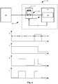
- Fig. 1 shows a block diagram of a device 10 according to the invention.
- the device 10 comprises a receiver 12 (for example a microcontroller) and a circuit 16 connected upstream of an input 14 of the receiver 12.
- the circuit 16 is set up in response to a control signal S of the receiver 12 which a sampling pause P indicates to reduce a current flow I along the signal path 18 by interrupting the signal path 18 by means of a switch 16a.
- the power loss when sampling a digital signal D, which is output by a transmitter 20, can thereby be reduced.
- a resistor can be arranged so that the current flow does not dry up completely even during the sampling pauses P and the input 14 does not become de-energized even during sampling pauses P.
- the read sample value can then be stored in a memory element 30 of the receiver 12, the memory element 30 being able to be overwritten with a new (current) value each time it is sampled.
- the receiver 12 can also read the sample value from the memory element 30 at any time and process it further.
- Fig. 3 shows a circuit diagram of a possible embodiment of a current limiting circuit 22 included in a device 10 according to the invention.
- the current limiting circuit 22 comprises a first transistor 24 placed in the signal path, which can be opened and closed by means of a control signal S.
- a sufficiently high switching voltage is applied to a base of a second transistor 26, the latter becomes conductive, as a result of which the voltage applied to the base of the first transistor 24 is reduced. Due to the reduced base voltage, the first transistor 24 becomes high-resistance and the current flow I through the first transistor 24 is reduced (sampling pause).
- the second transistor 26 becomes high-resistance, as a result of which the voltage applied to the base of the first transistor 24 increases.
- the first transistor 24 becomes low-resistance and the current flow I through the first transistor 24 is increased.
- the resulting current flow I through the first transistor 24 can be adapted to the input 14 of the receiver 12 by means of the dimensioning of the resistor 28. For example, an input voltage of 220 volts can be converted into an output voltage of 11 volts, as a result of which input 14 can be implemented with less powerful components.
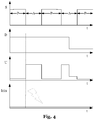
- Fig. 4 illustrated are checked whether the input 14 of the receiver 12 is working correctly. If, for example, despite the changeover between sampling pauses P and sampling phases A, no change in the signal lein read in by the receiver 12 can be inferred from this, that the input 14 of the receiver 12 is not working correctly. This can be particularly advantageous in the case of safety-related receivers 12.
- Fig. 5 illustrates that the display of individual sampling pauses P is suppressed (by means of the control signal S) if the sample value corresponds to a low level.
- the switching effort can be reduced without a significant increase in the power loss, since at a low level at which the current / voltage level of the digital signal D lies in a lower current / voltage level range, significantly less power loss occurs than at a high level , in which the digital signal is in an upper current / voltage level range.
- a sampling phase A can be ended immediately when a high level has been read in and stored in the memory 30 of the receiver 12, as a result of which the power loss can be reduced even further.
Landscapes
- Engineering & Computer Science (AREA)
- Microelectronics & Electronic Packaging (AREA)
- Physics & Mathematics (AREA)
- Nonlinear Science (AREA)
- Electromagnetism (AREA)
- General Physics & Mathematics (AREA)
- Radar, Positioning & Navigation (AREA)
- Automation & Control Theory (AREA)
- Power Engineering (AREA)
- Electronic Switches (AREA)
- Analogue/Digital Conversion (AREA)
Applications Claiming Priority (1)
| Application Number | Priority Date | Filing Date | Title |
|---|---|---|---|
| DE202019100080.5U DE202019100080U1 (de) | 2019-01-09 | 2019-01-09 | Vorrichtung zur Begrenzung einer Verlustleistung beim Abtasten eines digitalen Signals |
Publications (2)
| Publication Number | Publication Date |
|---|---|
| EP3680908A1 true EP3680908A1 (fr) | 2020-07-15 |
| EP3680908B1 EP3680908B1 (fr) | 2025-08-20 |
Family
ID=68965608
Family Applications (1)
| Application Number | Title | Priority Date | Filing Date |
|---|---|---|---|
| EP19217537.0A Active EP3680908B1 (fr) | 2019-01-09 | 2019-12-18 | Dispositif de limitation d'une dissipation de puissance lors du balayage d'un signal numérique |
Country Status (4)
| Country | Link |
|---|---|
| US (1) | US11152856B2 (fr) |
| EP (1) | EP3680908B1 (fr) |
| CN (1) | CN111431516A (fr) |
| DE (1) | DE202019100080U1 (fr) |
Citations (3)
| Publication number | Priority date | Publication date | Assignee | Title |
|---|---|---|---|---|
| US5410269A (en) * | 1992-05-27 | 1995-04-25 | Oki Electric Industry Co., Ltd. | Sample-and-hold circuit |
| US20080150590A1 (en) * | 2006-12-06 | 2008-06-26 | Cheng-Chung Hsu | Track and hold circuit |
| US20110002062A1 (en) * | 2003-11-21 | 2011-01-06 | Agere Systems Inc. | Analog multiplexer circuits and methods |
Family Cites Families (13)
| Publication number | Priority date | Publication date | Assignee | Title |
|---|---|---|---|---|
| JP3572844B2 (ja) * | 1997-01-28 | 2004-10-06 | 株式会社日立製作所 | 入力インタフェース回路及び入力インタフェース回路を用いた制御システム |
| DE69718129T2 (de) * | 1996-10-29 | 2003-10-23 | Hitachi, Ltd. | Redundantes Datenverarbeitungssystem |
| JP2006115003A (ja) * | 2004-10-12 | 2006-04-27 | Sony Corp | サンプルホールド回路およびそれを用いたパイプラインad変換器 |
| WO2009043044A1 (fr) * | 2007-09-28 | 2009-04-02 | Maxim Integrated Products, Inc. | Dispositif et circuit d'échantillonnage comportant une seule source de tension |
| US8390435B2 (en) * | 2009-08-07 | 2013-03-05 | General Electric Company | Apparatus for controlling integrated lighting ballasts in a series scheme |
| JP5308273B2 (ja) * | 2009-08-19 | 2013-10-09 | 旭化成エレクトロニクス株式会社 | サンプリングミキサ回路 |
| US8213187B2 (en) * | 2009-10-14 | 2012-07-03 | Power Integrations, Inc. | Method and apparatus for high-side input winding regulation |
| JP2012137422A (ja) * | 2010-12-27 | 2012-07-19 | Primearth Ev Energy Co Ltd | 電圧検出回路 |
| JP5898593B2 (ja) * | 2012-08-24 | 2016-04-06 | 日立オートモティブシステムズ株式会社 | モータ駆動回路、モータ駆動システム、電動パワーステアリングシステム、電動ブレーキシステム、車両駆動システム |
| EP2750275B1 (fr) * | 2012-12-31 | 2016-11-16 | Nxp B.V. | Surveillance de reseau avec des pertes faibles par suppression de l'échantillonnage pour un convertisseur commuté avec étape PFC |
| US8975953B2 (en) * | 2013-03-11 | 2015-03-10 | Analog Devices Global | Method of improving noise immunity in a signal processing apparatus, and a signal processing apparatus having improved noise immunity |
| US10250250B2 (en) * | 2016-09-12 | 2019-04-02 | Analog Devices, Inc. | Bootstrapped switching circuit |
| US11265006B2 (en) * | 2018-08-08 | 2022-03-01 | Infineon Technologies Ag | Using a sampling switch for multiple evaluation units |
-
2019
- 2019-01-09 DE DE202019100080.5U patent/DE202019100080U1/de active Active
- 2019-12-18 EP EP19217537.0A patent/EP3680908B1/fr active Active
-
2020
- 2020-01-06 CN CN202010010618.1A patent/CN111431516A/zh active Pending
- 2020-01-09 US US16/738,734 patent/US11152856B2/en active Active
Patent Citations (3)
| Publication number | Priority date | Publication date | Assignee | Title |
|---|---|---|---|---|
| US5410269A (en) * | 1992-05-27 | 1995-04-25 | Oki Electric Industry Co., Ltd. | Sample-and-hold circuit |
| US20110002062A1 (en) * | 2003-11-21 | 2011-01-06 | Agere Systems Inc. | Analog multiplexer circuits and methods |
| US20080150590A1 (en) * | 2006-12-06 | 2008-06-26 | Cheng-Chung Hsu | Track and hold circuit |
Also Published As
| Publication number | Publication date |
|---|---|
| DE202019100080U1 (de) | 2020-04-15 |
| CN111431516A (zh) | 2020-07-17 |
| EP3680908B1 (fr) | 2025-08-20 |
| US11152856B2 (en) | 2021-10-19 |
| US20200220459A1 (en) | 2020-07-09 |
Similar Documents
| Publication | Publication Date | Title |
|---|---|---|
| DE3415004C2 (fr) | ||
| DE102011054147B4 (de) | Testvorrichtung und Testverfahren | |
| DE3438674A1 (de) | Fuer die dynamische pruefung von schnellen datenwandlerkomponenten geeignete vorrichtung zum abtasten und digitalisieren von kurvenformen | |
| DE1762972B2 (de) | Steuerbare spannungsquelle | |
| DE2703880B2 (de) | Elektrisches Prüfgerät mit akustischer, quantitativer Analoganzeige für Widerstand und Spannung | |
| DE2150180C3 (de) | Vorrichtung zum Bestimmen der Steigung eines Signals | |
| DE1541868C3 (de) | Prüfgerät für elektronische Bauteile | |
| DE102008044908A1 (de) | Anordnung zur Messung wenigstens eines Wertes einer an einer elektronischen Komponente anliegenden Spannung | |
| DE202018105618U1 (de) | Kleinsignalspannungsquelle zum Verifizieren von Gleichstromzählern vom indirekten Zugriffstyp | |
| EP3680908A1 (fr) | Dispositif de limitation d'une dissipation de puissance lors du balayage d'un signal numérique | |
| EP0124761B1 (fr) | Dispositif pour tester des échantillons contenant des circuits électriques | |
| DE3101994A1 (de) | Verfahren und einrichtung zur messung eines elektrischen widerstandes | |
| EP3652860B1 (fr) | Convertisseur de niveau et procédé de conversion de valeurs de niveau dans des dispositifs de commande de véhicule | |
| WO2015197230A1 (fr) | Procédé et dispositif de détection de courants de faible intensité | |
| EP0964518A2 (fr) | Procédé pour l'ajustage des commutateurs de proximité | |
| DE3128306A1 (de) | Schaltungsvorrichtung zur digitalisierung und extremwertermittlung analoger signale | |
| CH658964A5 (de) | Analog/digital-wandler. | |
| DE1261880B (de) | Anordnung zum Abtasten und Festhalten von Spannungs-Augenblickswerten | |
| DE60001095T2 (de) | Serienschalter-treiberarchitektur für eine automatische testeinrichtung | |
| DE960219C (de) | Verfahren zur Messung bzw. Kontrolle der mittleren Verzerrungen von Gleichstrom-Steuer-Impulsen niedriger Impulsfolge, die durch Einrichtungen fuer die Impulsuebertragung verursacht werden | |
| AT284270B (de) | Schaltungsanordnung zum selbsttätigen Messen der Parameter von Schaltungselementen der Fernmeldetechnik, die während dieser Messung von einem seine Eigenschaften periodisch wechselnden Strom gespeist werden | |
| DE1762972C (de) | Steuerbare Spannungsquelle Ausscheidung aus 1537966 | |
| DE2027064C (de) | Prüfanordnung für einen Ionisations-Rauchfühler | |
| EP0626585A1 (fr) | Appareil de mesure de transistor programmable et totalement électronique | |
| DE2311012C3 (de) | Elektrisches Prüfgerät mit akustischer, quantitativer Analoganzeige für Widerstand und Spannung |
Legal Events
| Date | Code | Title | Description |
|---|---|---|---|
| PUAI | Public reference made under article 153(3) epc to a published international application that has entered the european phase |
Free format text: ORIGINAL CODE: 0009012 |
|
| STAA | Information on the status of an ep patent application or granted ep patent |
Free format text: STATUS: THE APPLICATION HAS BEEN PUBLISHED |
|
| AK | Designated contracting states |
Kind code of ref document: A1 Designated state(s): AL AT BE BG CH CY CZ DE DK EE ES FI FR GB GR HR HU IE IS IT LI LT LU LV MC MK MT NL NO PL PT RO RS SE SI SK SM TR |
|
| AX | Request for extension of the european patent |
Extension state: BA ME |
|
| STAA | Information on the status of an ep patent application or granted ep patent |
Free format text: STATUS: REQUEST FOR EXAMINATION WAS MADE |
|
| 17P | Request for examination filed |
Effective date: 20210113 |
|
| RBV | Designated contracting states (corrected) |
Designated state(s): AL AT BE BG CH CY CZ DE DK EE ES FI FR GB GR HR HU IE IS IT LI LT LU LV MC MK MT NL NO PL PT RO RS SE SI SK SM TR |
|
| STAA | Information on the status of an ep patent application or granted ep patent |
Free format text: STATUS: EXAMINATION IS IN PROGRESS |
|
| 17Q | First examination report despatched |
Effective date: 20230405 |
|
| P01 | Opt-out of the competence of the unified patent court (upc) registered |
Effective date: 20230524 |
|
| GRAP | Despatch of communication of intention to grant a patent |
Free format text: ORIGINAL CODE: EPIDOSNIGR1 |
|
| STAA | Information on the status of an ep patent application or granted ep patent |
Free format text: STATUS: GRANT OF PATENT IS INTENDED |
|
| INTG | Intention to grant announced |
Effective date: 20250403 |
|
| RAP3 | Party data changed (applicant data changed or rights of an application transferred) |
Owner name: WAGO VERWALTUNGSGESELLSCHAFT MBH |
|
| GRAS | Grant fee paid |
Free format text: ORIGINAL CODE: EPIDOSNIGR3 |
|
| GRAA | (expected) grant |
Free format text: ORIGINAL CODE: 0009210 |
|
| STAA | Information on the status of an ep patent application or granted ep patent |
Free format text: STATUS: THE PATENT HAS BEEN GRANTED |
|
| AK | Designated contracting states |
Kind code of ref document: B1 Designated state(s): AL AT BE BG CH CY CZ DE DK EE ES FI FR GB GR HR HU IE IS IT LI LT LU LV MC MK MT NL NO PL PT RO RS SE SI SK SM TR |
|
| REG | Reference to a national code |
Ref country code: GB Ref legal event code: FG4D Free format text: NOT ENGLISH |
|
| REG | Reference to a national code |
Ref country code: CH Ref legal event code: EP |
|
| REG | Reference to a national code |
Ref country code: DE Ref legal event code: R096 Ref document number: 502019013789 Country of ref document: DE |
|
| REG | Reference to a national code |
Ref country code: IE Ref legal event code: FG4D Free format text: LANGUAGE OF EP DOCUMENT: GERMAN |
|
| REG | Reference to a national code |
Ref country code: NL Ref legal event code: MP Effective date: 20250820 |
|
| REG | Reference to a national code |
Ref country code: CH Ref legal event code: U11 Free format text: ST27 STATUS EVENT CODE: U-0-0-U10-U11 (AS PROVIDED BY THE NATIONAL OFFICE) Effective date: 20260101 |
|
| PG25 | Lapsed in a contracting state [announced via postgrant information from national office to epo] |
Ref country code: IS Free format text: LAPSE BECAUSE OF FAILURE TO SUBMIT A TRANSLATION OF THE DESCRIPTION OR TO PAY THE FEE WITHIN THE PRESCRIBED TIME-LIMIT Effective date: 20251220 |
|
| PGFP | Annual fee paid to national office [announced via postgrant information from national office to epo] |
Ref country code: GB Payment date: 20251223 Year of fee payment: 7 |
|
| PG25 | Lapsed in a contracting state [announced via postgrant information from national office to epo] |
Ref country code: NO Free format text: LAPSE BECAUSE OF FAILURE TO SUBMIT A TRANSLATION OF THE DESCRIPTION OR TO PAY THE FEE WITHIN THE PRESCRIBED TIME-LIMIT Effective date: 20251120 |
|
| REG | Reference to a national code |
Ref country code: LT Ref legal event code: MG9D |
|
| PG25 | Lapsed in a contracting state [announced via postgrant information from national office to epo] |
Ref country code: PT Free format text: LAPSE BECAUSE OF FAILURE TO SUBMIT A TRANSLATION OF THE DESCRIPTION OR TO PAY THE FEE WITHIN THE PRESCRIBED TIME-LIMIT Effective date: 20251222 |
|
| PG25 | Lapsed in a contracting state [announced via postgrant information from national office to epo] |
Ref country code: FI Free format text: LAPSE BECAUSE OF FAILURE TO SUBMIT A TRANSLATION OF THE DESCRIPTION OR TO PAY THE FEE WITHIN THE PRESCRIBED TIME-LIMIT Effective date: 20250820 |
|
| PG25 | Lapsed in a contracting state [announced via postgrant information from national office to epo] |
Ref country code: NL Free format text: LAPSE BECAUSE OF FAILURE TO SUBMIT A TRANSLATION OF THE DESCRIPTION OR TO PAY THE FEE WITHIN THE PRESCRIBED TIME-LIMIT Effective date: 20250820 Ref country code: HR Free format text: LAPSE BECAUSE OF FAILURE TO SUBMIT A TRANSLATION OF THE DESCRIPTION OR TO PAY THE FEE WITHIN THE PRESCRIBED TIME-LIMIT Effective date: 20250820 |
|
| PG25 | Lapsed in a contracting state [announced via postgrant information from national office to epo] |
Ref country code: GR Free format text: LAPSE BECAUSE OF FAILURE TO SUBMIT A TRANSLATION OF THE DESCRIPTION OR TO PAY THE FEE WITHIN THE PRESCRIBED TIME-LIMIT Effective date: 20251121 |
|
| PG25 | Lapsed in a contracting state [announced via postgrant information from national office to epo] |
Ref country code: SE Free format text: LAPSE BECAUSE OF FAILURE TO SUBMIT A TRANSLATION OF THE DESCRIPTION OR TO PAY THE FEE WITHIN THE PRESCRIBED TIME-LIMIT Effective date: 20250820 |
|
| PG25 | Lapsed in a contracting state [announced via postgrant information from national office to epo] |
Ref country code: LV Free format text: LAPSE BECAUSE OF FAILURE TO SUBMIT A TRANSLATION OF THE DESCRIPTION OR TO PAY THE FEE WITHIN THE PRESCRIBED TIME-LIMIT Effective date: 20250820 |
|
| PG25 | Lapsed in a contracting state [announced via postgrant information from national office to epo] |
Ref country code: PL Free format text: LAPSE BECAUSE OF FAILURE TO SUBMIT A TRANSLATION OF THE DESCRIPTION OR TO PAY THE FEE WITHIN THE PRESCRIBED TIME-LIMIT Effective date: 20250820 Ref country code: BG Free format text: LAPSE BECAUSE OF FAILURE TO SUBMIT A TRANSLATION OF THE DESCRIPTION OR TO PAY THE FEE WITHIN THE PRESCRIBED TIME-LIMIT Effective date: 20250820 |
|
| PG25 | Lapsed in a contracting state [announced via postgrant information from national office to epo] |
Ref country code: RS Free format text: LAPSE BECAUSE OF FAILURE TO SUBMIT A TRANSLATION OF THE DESCRIPTION OR TO PAY THE FEE WITHIN THE PRESCRIBED TIME-LIMIT Effective date: 20251120 |
|
| PG25 | Lapsed in a contracting state [announced via postgrant information from national office to epo] |
Ref country code: ES Free format text: LAPSE BECAUSE OF FAILURE TO SUBMIT A TRANSLATION OF THE DESCRIPTION OR TO PAY THE FEE WITHIN THE PRESCRIBED TIME-LIMIT Effective date: 20250820 |
|
| PG25 | Lapsed in a contracting state [announced via postgrant information from national office to epo] |
Ref country code: RO Free format text: LAPSE BECAUSE OF FAILURE TO SUBMIT A TRANSLATION OF THE DESCRIPTION OR TO PAY THE FEE WITHIN THE PRESCRIBED TIME-LIMIT Effective date: 20250820 |
|
| PG25 | Lapsed in a contracting state [announced via postgrant information from national office to epo] |
Ref country code: SM Free format text: LAPSE BECAUSE OF FAILURE TO SUBMIT A TRANSLATION OF THE DESCRIPTION OR TO PAY THE FEE WITHIN THE PRESCRIBED TIME-LIMIT Effective date: 20250820 |
|
| PG25 | Lapsed in a contracting state [announced via postgrant information from national office to epo] |
Ref country code: DK Free format text: LAPSE BECAUSE OF FAILURE TO SUBMIT A TRANSLATION OF THE DESCRIPTION OR TO PAY THE FEE WITHIN THE PRESCRIBED TIME-LIMIT Effective date: 20250820 |
|
| PGFP | Annual fee paid to national office [announced via postgrant information from national office to epo] |
Ref country code: DE Payment date: 20251229 Year of fee payment: 7 |
|
| PG25 | Lapsed in a contracting state [announced via postgrant information from national office to epo] |
Ref country code: IT Free format text: LAPSE BECAUSE OF FAILURE TO SUBMIT A TRANSLATION OF THE DESCRIPTION OR TO PAY THE FEE WITHIN THE PRESCRIBED TIME-LIMIT Effective date: 20250820 |
|
| PG25 | Lapsed in a contracting state [announced via postgrant information from national office to epo] |
Ref country code: CZ Free format text: LAPSE BECAUSE OF FAILURE TO SUBMIT A TRANSLATION OF THE DESCRIPTION OR TO PAY THE FEE WITHIN THE PRESCRIBED TIME-LIMIT Effective date: 20250820 |
|
| PGFP | Annual fee paid to national office [announced via postgrant information from national office to epo] |
Ref country code: CH Payment date: 20260101 Year of fee payment: 7 |
|
| PG25 | Lapsed in a contracting state [announced via postgrant information from national office to epo] |
Ref country code: SK Free format text: LAPSE BECAUSE OF FAILURE TO SUBMIT A TRANSLATION OF THE DESCRIPTION OR TO PAY THE FEE WITHIN THE PRESCRIBED TIME-LIMIT Effective date: 20250820 Ref country code: EE Free format text: LAPSE BECAUSE OF FAILURE TO SUBMIT A TRANSLATION OF THE DESCRIPTION OR TO PAY THE FEE WITHIN THE PRESCRIBED TIME-LIMIT Effective date: 20250820 |