EP3694008B1 - Hybridstruktur für vorrichtung mit oberflächenschallwellen - Google Patents
Hybridstruktur für vorrichtung mit oberflächenschallwellen Download PDFInfo
- Publication number
- EP3694008B1 EP3694008B1 EP20165678.2A EP20165678A EP3694008B1 EP 3694008 B1 EP3694008 B1 EP 3694008B1 EP 20165678 A EP20165678 A EP 20165678A EP 3694008 B1 EP3694008 B1 EP 3694008B1
- Authority
- EP
- European Patent Office
- Prior art keywords
- layer
- hybrid structure
- acoustic wave
- surface acoustic
- wave device
- Prior art date
- Legal status (The legal status is an assumption and is not a legal conclusion. Google has not performed a legal analysis and makes no representation as to the accuracy of the status listed.)
- Active
Links
Images



Classifications
-
- H—ELECTRICITY
- H03—ELECTRONIC CIRCUITRY
- H03H—IMPEDANCE NETWORKS, e.g. RESONANT CIRCUITS; RESONATORS
- H03H9/00—Networks comprising electromechanical or electro-acoustic elements; Electromechanical resonators
- H03H9/02—Details
- H03H9/02535—Details of surface acoustic wave devices
- H03H9/02614—Treatment of substrates, e.g. curved, spherical, cylindrical substrates ensuring closed round-about circuits for the acoustical waves
- H03H9/02622—Treatment of substrates, e.g. curved, spherical, cylindrical substrates ensuring closed round-about circuits for the acoustical waves of the surface, including back surface
-
- H—ELECTRICITY
- H03—ELECTRONIC CIRCUITRY
- H03H—IMPEDANCE NETWORKS, e.g. RESONANT CIRCUITS; RESONATORS
- H03H9/00—Networks comprising electromechanical or electro-acoustic elements; Electromechanical resonators
- H03H9/02—Details
- H03H9/02535—Details of surface acoustic wave devices
- H03H9/02543—Characteristics of substrate, e.g. cutting angles
- H03H9/02559—Characteristics of substrate, e.g. cutting angles of lithium niobate or lithium-tantalate substrates
-
- H—ELECTRICITY
- H03—ELECTRONIC CIRCUITRY
- H03H—IMPEDANCE NETWORKS, e.g. RESONANT CIRCUITS; RESONATORS
- H03H9/00—Networks comprising electromechanical or electro-acoustic elements; Electromechanical resonators
- H03H9/02—Details
- H03H9/02535—Details of surface acoustic wave devices
- H03H9/02543—Characteristics of substrate, e.g. cutting angles
- H03H9/02566—Characteristics of substrate, e.g. cutting angles of semiconductor substrates
-
- H—ELECTRICITY
- H03—ELECTRONIC CIRCUITRY
- H03H—IMPEDANCE NETWORKS, e.g. RESONANT CIRCUITS; RESONATORS
- H03H9/00—Networks comprising electromechanical or electro-acoustic elements; Electromechanical resonators
- H03H9/02—Details
- H03H9/02535—Details of surface acoustic wave devices
- H03H9/02543—Characteristics of substrate, e.g. cutting angles
- H03H9/02574—Characteristics of substrate, e.g. cutting angles of combined substrates, multilayered substrates, piezoelectrical layers on not-piezoelectrical substrate
-
- H—ELECTRICITY
- H03—ELECTRONIC CIRCUITRY
- H03H—IMPEDANCE NETWORKS, e.g. RESONANT CIRCUITS; RESONATORS
- H03H9/00—Networks comprising electromechanical or electro-acoustic elements; Electromechanical resonators
- H03H9/02—Details
- H03H9/02535—Details of surface acoustic wave devices
- H03H9/02818—Means for compensation or elimination of undesirable effects
-
- H—ELECTRICITY
- H03—ELECTRONIC CIRCUITRY
- H03H—IMPEDANCE NETWORKS, e.g. RESONANT CIRCUITS; RESONATORS
- H03H9/00—Networks comprising electromechanical or electro-acoustic elements; Electromechanical resonators
- H03H9/02—Details
- H03H9/02535—Details of surface acoustic wave devices
- H03H9/02818—Means for compensation or elimination of undesirable effects
- H03H9/02834—Means for compensation or elimination of undesirable effects of temperature influence
-
- H—ELECTRICITY
- H03—ELECTRONIC CIRCUITRY
- H03H—IMPEDANCE NETWORKS, e.g. RESONANT CIRCUITS; RESONATORS
- H03H9/00—Networks comprising electromechanical or electro-acoustic elements; Electromechanical resonators
- H03H9/02—Details
- H03H9/02535—Details of surface acoustic wave devices
- H03H9/0296—Surface acoustic wave [SAW] devices having both acoustic and non-acoustic properties
-
- H—ELECTRICITY
- H10—SEMICONDUCTOR DEVICES; ELECTRIC SOLID-STATE DEVICES NOT OTHERWISE PROVIDED FOR
- H10N—ELECTRIC SOLID-STATE DEVICES NOT OTHERWISE PROVIDED FOR
- H10N30/00—Piezoelectric or electrostrictive devices
- H10N30/01—Manufacture or treatment
- H10N30/07—Forming of piezoelectric or electrostrictive parts or bodies on an electrical element or another base
- H10N30/072—Forming of piezoelectric or electrostrictive parts or bodies on an electrical element or another base by laminating or bonding of piezoelectric or electrostrictive bodies
- H10N30/073—Forming of piezoelectric or electrostrictive parts or bodies on an electrical element or another base by laminating or bonding of piezoelectric or electrostrictive bodies by fusion of metals or by adhesives
-
- H—ELECTRICITY
- H10—SEMICONDUCTOR DEVICES; ELECTRIC SOLID-STATE DEVICES NOT OTHERWISE PROVIDED FOR
- H10N—ELECTRIC SOLID-STATE DEVICES NOT OTHERWISE PROVIDED FOR
- H10N30/00—Piezoelectric or electrostrictive devices
- H10N30/50—Piezoelectric or electrostrictive devices having a stacked or multilayer structure
-
- H—ELECTRICITY
- H10—SEMICONDUCTOR DEVICES; ELECTRIC SOLID-STATE DEVICES NOT OTHERWISE PROVIDED FOR
- H10N—ELECTRIC SOLID-STATE DEVICES NOT OTHERWISE PROVIDED FOR
- H10N30/00—Piezoelectric or electrostrictive devices
- H10N30/704—Piezoelectric or electrostrictive devices based on piezoelectric or electrostrictive films or coatings
- H10N30/706—Piezoelectric or electrostrictive devices based on piezoelectric or electrostrictive films or coatings characterised by the underlying bases, e.g. substrates
- H10N30/708—Intermediate layers, e.g. barrier, adhesion or growth control buffer layers
-
- H—ELECTRICITY
- H10—SEMICONDUCTOR DEVICES; ELECTRIC SOLID-STATE DEVICES NOT OTHERWISE PROVIDED FOR
- H10N—ELECTRIC SOLID-STATE DEVICES NOT OTHERWISE PROVIDED FOR
- H10N30/00—Piezoelectric or electrostrictive devices
- H10N30/80—Constructional details
- H10N30/85—Piezoelectric or electrostrictive active materials
- H10N30/853—Ceramic compositions
- H10N30/8542—Alkali metal based oxides, e.g. lithium, sodium or potassium niobates
-
- H—ELECTRICITY
- H10—SEMICONDUCTOR DEVICES; ELECTRIC SOLID-STATE DEVICES NOT OTHERWISE PROVIDED FOR
- H10P—GENERIC PROCESSES OR APPARATUS FOR THE MANUFACTURE OR TREATMENT OF DEVICES COVERED BY CLASS H10
- H10P90/00—Preparation of wafers not covered by a single main group of this subclass, e.g. wafer reinforcement
- H10P90/19—Preparing inhomogeneous wafers
- H10P90/1904—Preparing vertically inhomogeneous wafers
- H10P90/1906—Preparing SOI wafers
- H10P90/1914—Preparing SOI wafers using bonding
- H10P90/1916—Preparing SOI wafers using bonding with separation or delamination along an ion implanted layer, e.g. Smart-cut
-
- H—ELECTRICITY
- H10—SEMICONDUCTOR DEVICES; ELECTRIC SOLID-STATE DEVICES NOT OTHERWISE PROVIDED FOR
- H10P—GENERIC PROCESSES OR APPARATUS FOR THE MANUFACTURE OR TREATMENT OF DEVICES COVERED BY CLASS H10
- H10P90/00—Preparation of wafers not covered by a single main group of this subclass, e.g. wafer reinforcement
- H10P90/19—Preparing inhomogeneous wafers
- H10P90/1904—Preparing vertically inhomogeneous wafers
- H10P90/1906—Preparing SOI wafers
- H10P90/1914—Preparing SOI wafers using bonding
- H10P90/1918—Preparing SOI wafers using bonding including charge trapping layers, e.g. polycrystalline materials
-
- H—ELECTRICITY
- H10—SEMICONDUCTOR DEVICES; ELECTRIC SOLID-STATE DEVICES NOT OTHERWISE PROVIDED FOR
- H10W—GENERIC PACKAGES, INTERCONNECTIONS, CONNECTORS OR OTHER CONSTRUCTIONAL DETAILS OF DEVICES COVERED BY CLASS H10
- H10W10/00—Isolation regions in semiconductor bodies between components of integrated devices
- H10W10/10—Isolation regions comprising dielectric materials
- H10W10/181—Semiconductor-on-insulator [SOI] isolation regions, e.g. buried oxide regions of SOI wafers
-
- H—ELECTRICITY
- H03—ELECTRONIC CIRCUITRY
- H03H—IMPEDANCE NETWORKS, e.g. RESONANT CIRCUITS; RESONATORS
- H03H9/00—Networks comprising electromechanical or electro-acoustic elements; Electromechanical resonators
- H03H2009/0019—Surface acoustic wave multichip
Definitions
- the present invention relates to the field of surface acoustic wave devices. It relates in particular to a hybrid structure suitable for manufacturing surface acoustic wave devices and a method of manufacturing said hybrid structure.
- SAW Surface acoustic wave devices
- SAW Surface acoustic wave devices
- RF Radio Frequency
- BAW Bulk Acoustic Wave
- TCF coefficient of thermal frequency
- One approach consists in using a hybrid substrate, for example composed of a layer of piezoelectric material disposed on a silicon substrate.
- the low CTE of silicon makes it possible to limit the expansion / contraction of the piezoelectric layer in temperature.
- a piezoelectric layer of Lithium Tantalate (LiTaO3) the article cited above indicates that a ratio of 10 between the thickness of LiTaO3 and the thickness of the silicon substrate makes it possible to suitably improve the coefficient of thermal frequency (TCF).
- the document DE102004045181 also discloses a structure suitable for SAW applications, comprising a piezoelectric layer placed on a compensation layer (for example silicon).
- a compensation layer for example silicon
- One solution for reducing these parasitic resonances is to increase the thickness of the LiTaO3 layer; this supposing also to increase the thickness of the Si substrate in order to maintain the improvements of the TCF, the total thickness of the hybrid substrate is then no longer compatible with the needs for reducing the thickness of the final components, in particular to address the market cell phones.
- Another solution, proposed by K. Hashimoto is to roughen the lower surface of the LiTaO3 layer so as to limit the reflections of the acoustic wave on it. Such roughening represents a difficulty to be managed when a direct bonding process, requiring very smooth surfaces to be assembled, is used to produce the hybrid substrate.
- Another drawback of a hybrid substrate according to the state of the art comes from the presence of the support made of semiconductor silicon material, which, even highly resistive, is liable to contain mobile charges and to impact the performance of the device, in particular by increasing the insertion losses and the distortions (linearity) of the RF signal compared to a solid piezoelectric substrate.
- the document WO2016 / 087728 offers a structure comprising a trapping layer characterized by a specific defect density, arranged on the support substrate.
- An object of the present invention is to remedy all or part of the drawbacks of the prior art.
- An object of the invention is to provide a hybrid structure allowing the reduction and / or elimination of said parasitic acoustic waves and ensuring stable performance for devices operating at high frequencies.
- the trapping layer of the hybrid structure according to the invention effectively traps the mobile electric charges potentially generated in the support substrate during the operation of the SAW RF device produced on said hybrid structure.
- RF performance linearity, insertion losses
- RF performance thus reach a good level, comparable or even superior to that of technologies on massive piezoelectric substrates.
- the functional interface of determined roughness allows efficient diffusion of the acoustic waves capable of propagating in depth in the useful layer, thus avoiding their parasitic reflections which are known to negatively impact the quality of the signal of the SAW device.
- This diffusion of acoustic waves is made more efficient because the functional interface is located between the useful layer and the trapping layer: in fact, in addition to its qualities of trapping mobile charges, the trapping layer makes it possible to effectively screen the 'underlying interface with the support substrate, the latter contributing in hybrid structures to reflect acoustic waves.
- the present invention also relates to a surface acoustic wave device comprising a hybrid structure as above.
- the figures are schematic representations which, for the sake of readability, are not to scale.
- the thicknesses of the layers along the z axis are not to scale with respect to the lateral dimensions along the x and y axes.
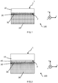
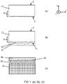
- the invention relates to a hybrid structure 100 for a surface acoustic wave device comprising a useful layer 10 of piezoelectric material having a free first face 1 and a second face 2.
- the useful layer 10 comprises a piezoelectric material chosen, as a example, from lithium tantalate (LiTaO3), lithium niobate (LiNbO3), quartz, zinc oxide (ZnO), aluminum nitride (AlN).
- the useful layer 10 is placed on a support substrate 20, the coefficient of thermal expansion of which is lower than that of the useful layer 10.
- the support substrate 20 is, by way of example, formed of silicon or germanium.
- the thickness of the trapping layer 30 may be between a few tens of nm and a few microns, or even a few tens of microns.
- the trapping layer 30 is directly in contact with the support substrate 20, which allows effective trapping of the mobile charges generated in the support substrate 20.
- the hybrid structure 100 according to the invention further comprises at least one functional interface 31 of determined roughness between the useful layer 10 and the trapping layer 30.
- the roughness of the functional interface 31 is defined by the maximum peak-to-valley amplitude, measured for example by mechanical or optical profilometry, on measurement profiles of the order of 50 to 500 ⁇ m or measurement surfaces of the order of 50x50 to 500x500 ⁇ m2.
- the determined peak-to-valley roughness is greater than 0.3 ⁇ m.
- it is even greater than or equal to 0.5 ⁇ m, or even to 1 ⁇ m. It is preferably between 0.3 and 5 ⁇ m.
- the spectral density (PSD) of the roughness of the functional interface 31 covers all or part of the spectral band of wavelengths of the parasitic waves which it is sought to eliminate.
- the determined roughness has spatial wavelengths and an amplitude at least equal to a quarter of the parasitic wavelengths.
- the determined roughness of the functional interface 31 can therefore be adapted in amplitude and potentially in spectral density as a function of the frequency of the acoustic waves of the SAW device which will be manufactured on the hybrid structure 100, for its ability to efficiently diffuse the acoustic waves liable to to propagate in the useful layer 10.
- the trapping layer 30 of the hybrid structure 100 effectively traps the mobile electrical charges potentially generated in the support substrate 20 during the operation of the SAW RF device produced on the first face 1 of said hybrid structure 100.
- the RF performance ( linearity, insertion losses) thus reach a very good level, comparable or even superior to that of technologies on massive piezoelectric substrates.
- the functional interface 31 of determined roughness allows efficient diffusion of the acoustic waves capable of propagating in depth in the useful layer 10, avoiding thus their parasitic reflections, which are known to negatively impact the signal quality of the SAW device.
- the functional interface 31 is formed by the interface between the useful layer 10 and the trapping layer 30.
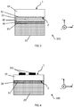
- the functional interface 31 is formed by the interface between a first intermediate layer 40, arranged on the second face 2 of the useful layer 10, and the trapping layer 30.
- the first intermediate layer 40 can comprise a material chosen from silicon oxide, silicon nitride, silicon oxynitride or even a material of the same type as the useful layer.
- the trapping layer 30 makes it possible to move away and screen the underlying interface with the support substrate 20, the latter being a strong contributor, in the usual hybrid structures, to the reflection of the acoustic waves propagating in the volume of the useful layer 10.
- the interface with the support substrate 20 is screened in the sense that the majority, or even all, of the acoustic waves reaching the functional interface 31 will be efficiently diffused by the latter and thus never reach this interface.
- the hybrid structure 100 comprises a second functional interface 32 having a second determined roughness, the peak-to-valley amplitude of which is greater than 0.1 ⁇ m. It is preferably between 0.1 and 5 ⁇ m.
- the second functional interface 32 may have a second determined roughness different from the determined roughness of the first functional interface 31, both in amplitude and in spectral density.
- the spectral densities can be chosen to cover in a complementary manner the spectral band of wavelengths of the parasitic waves that it is desired to eliminate.
- the second functional interface 32 is formed by the interface between the useful layer 10 and a second intermediate layer 50 arranged on the first intermediate layer 40.
- the second intermediate layer 50 comprises a material chosen from the oxide of silicon, silicon nitride, silicon oxynitride; it can also comprise a material of the same type as that constituting the useful layer 10: for a useful layer 10 of LiTaO3, the second intermediate layer 50 may for example consist of a deposited amorphous LiTaO3 layer.
- the first 40 and second 50 intermediate layers are formed of the same material; thus, the interface between these two layers contributes little or little to parasitic reflections, due to the absence of an acoustic impedance difference between the two layers.
- the support substrate is a solid substrate.
- it could consist of a composite substrate comprising at least one virgin layer or a structured layer, comprising all or part of microelectronic components; these configurations are particularly advantageous for producing co-integrated systems, including surface acoustic wave devices in and on the useful layer 10, and components (switches, amplifiers, other filters, etc.) in the support substrate.
- the invention also relates to a surface acoustic wave device 200 comprising a hybrid structure 100, illustrated in figure 4 .
- the device 200 comprises, for example, interdigitated metal electrodes 201 on the first face 1 of the useful layer 10, between which the acoustic wave will propagate.
- the hybrid structure 100 is particularly suitable for manufacturing surface acoustic wave devices 200 using acoustic wave frequencies between 700 MHz and 3GHz.
- the disclosure also relates to a method of manufacturing a hybrid structure 100 for a surface acoustic wave device 200, which will be described with reference to figures 5 to 7, this process not forming part of the invention.
- the manufacturing method firstly comprises a step of providing a useful layer 10 of piezoelectric material comprising a first face 1 and a second face 2 having a determined roughness.
- Said roughness is defined by the maximum peak-to-valley amplitude, measured for example by mechanical or optical profilometry, on measurement profiles of the order of 50 to 500 ⁇ m or measurement surfaces of the order of 50x50 to 500x500 ⁇ m2.
- the determined roughness is greater than 0.3 ⁇ m, or even greater than or equal to 0.5 microns, or even greater than 1 ⁇ m. Preferably, it is even between 0.3 and 5 ⁇ m.
- the spectral density of the roughness of the functional interface 31 covers all or part of the spectral band of wavelengths of the parasitic waves which it is sought to eliminate.
- the determined roughness has spatial wavelengths and an amplitude at least equal to a quarter of the parasitic wavelengths.
- the determined roughness of the functional interface 31 can therefore be adapted in amplitude and potentially in spectral density as a function of the frequency of the acoustic waves of the SAW device which will be manufactured on the hybrid structure 100, for its ability to efficiently diffuse the acoustic waves liable to to propagate in the useful layer 10.
- the determined roughness can be achieved on the second face 2 by mechanical lapping techniques, mechanical-chemical polishing, wet or dry chemical etching, or a combination of these different techniques.
- the objective is to create on the second face 2 of the useful layer 10 a uniform roughness over the entire face, of determined amplitude.
- such roughness can be obtained by the typical treatments of frosted rear faces of wafers (lithium tantalate, lithium niobate, etc.) used in the semiconductor industry.
- the useful layer 10 comprises a piezoelectric material chosen from lithium tantalate (LiTaO3), lithium niobate (LiNbO3), quartz, zinc oxide (ZnO), nitride aluminum (AlN).
- a piezoelectric material chosen from lithium tantalate (LiTaO3), lithium niobate (LiNbO3), quartz, zinc oxide (ZnO), nitride aluminum (AlN).
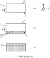
- the useful layer 10 is included in a donor substrate 11, having a second face 2 of determined roughness and a first face 1 '( figure 5a ).
- the exemplary manufacturing process also comprises a step of forming a trapping layer 30 on the second face 2 of the useful layer 10, or of the donor substrate 11 ( figure 5b ).
- the interface between the trapping layer 30 and the useful layer 10 (or the donor substrate 11) forms a functional interface 31 of determined roughness.
- the trapping layer 30 is formed from a material chosen from amorphous silicon, polycrystalline silicon, germanium. amorphous or polycrystalline.
- the trapping layer 30 can be produced by known techniques of chemical deposition (PECVD, LPCVD, etc.).
- the trapping layer 30 typically has a thickness of between a few tens of nm and a few ⁇ m, or even a few tens of ⁇ m.
- the step of forming the trapping layer 30 comprises a step of smoothing the free surface of the trapping layer 30, consisting for example of mechanical-chemical polishing, smooth etching by plasma or wet chemical etching.
- the free surface of the trapping layer 30 will exhibit low roughness (typically ⁇ 0.5 nm RMS, measured by atomic force microscopy) and good flatness, with a view to a subsequent assembly step.
- the manufacturing method also comprises a step of providing a support substrate 20 ( figure 5c ) exhibiting a thermal expansion coefficient lower than that of the useful layer 10.
- the support substrate 20 is made of silicon, this material being widely available and compatible with the semiconductor industry. Alternatively, it could also be made of germanium or another material compatible with the subsequent steps of the process and of the development of the surface acoustic wave device.
- the manufacturing process then comprises an assembly step for placing the donor substrate 11 (or the useful layer 10) on the support substrate 20 ( figure 5d ).
- the assembly step takes place between the trapping layer 30 and the support substrate 20, which is why the surface properties of the trapping layer 30 and the support substrate 20 must be properly controlled.
- the assembly step comprises direct bonding by molecular adhesion: this bonding technique is preferred in that it does not require the use of an additional layer of material.
- the assembly step may comprise an adhesive bonding, a metallic bonding, an anodic bonding, or any other kind of bonding known from the state of the art and compatible with the intended application.
- the assembly step comprises, prior to bonding, a cleaning sequence to ensure a good level of cleanliness (removal of particles, hydrocarbon and metal contaminants, etc.) to the surfaces before bonding.
- a layer of the same nature as the trapping layer 30 may be deposited on the support substrate 20 prior to the assembly step, and will be prepared with a view to being bonded to the trapping layer 30.
- it may be advantageous, in particular in the case of direct bonding by molecular adhesion, to form a bonding interface between two materials of the same nature.
- the bonded hybrid structure 101 can be subjected to heat treatment. It should be noted that the materials of the donor substrate 11 (or of the useful layer 10) and of the support substrate 20 have very different thermal expansion coefficients, the heat treatment applied must therefore remain at a temperature below the damage temperature. or breakage of the bonded structure 101.
- the temperature range is typically between a few tens of degrees and 500 ° C.
- the manufacturing method further comprises a step of thinning the donor substrate 11 ( figure 5e ) to form the useful layer 10 and the first face 1, on which the surface acoustic wave devices will be produced.
- an exemplary hybrid structure 100 is obtained which does not form part of the invention ( figure 5e ).
- the invention relates to a method of manufacturing a hybrid structure 100 for a surface acoustic wave device comprising firstly a step of providing a useful layer 10 of piezoelectric material comprising a first face 1 and a second face 2. .
- the useful layer 10 comprises a piezoelectric material chosen from lithium tantalate (LiTaO3), lithium niobate (LiNbO3), quartz, zinc oxide (ZnO), nitride aluminum (AlN).
- a piezoelectric material chosen from lithium tantalate (LiTaO3), lithium niobate (LiNbO3), quartz, zinc oxide (ZnO), nitride aluminum (AlN).
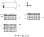
- the useful layer 10 is included in a donor substrate 11, having a second face 2 and a first face 1 '( figure 6a ).
- the manufacturing method also comprises a step of providing a support substrate 20 having a thermal expansion coefficient lower than that of the useful layer 10.
- the support substrate 20 is made of silicon, this material being widely available and compatible with the. semiconductor industry. As mentioned above, it could alternatively be formed or comprise germanium or other material compatible with the subsequent manufacturing steps.
- the manufacturing process also comprises a step of forming a trapping layer 30 on the support substrate 20 ( figure 6b ).
- the trapping layer 30 has a determined roughness.
- the trapping layer 30 is formed from a material chosen from amorphous silicon, poly-crystalline silicon, amorphous or poly-crystalline germanium. It can be produced by known techniques of chemical deposition (CVD).
- the trapping layer 30 may have a thickness of between a few tens of nm and a few ⁇ m, or even a few tens of ⁇ m.
- the roughness of the free surface of the trapping layer 30, after its formation on the support substrate 20, is defined by the maximum peak-to-valley amplitude, measured for example by mechanical or optical profilometry, on measurement profiles of the order of 50 to 500 ⁇ m or measuring surfaces of the order of 50x50 to 500x500 ⁇ m2.
- the determined roughness is greater than 0.3 ⁇ m, or even greater than or equal to 0.5 ⁇ m, or even greater than or equal to 1 ⁇ m. It is preferably between 0.3 and 5 ⁇ m.
- the spectral density of the roughness of the functional interface 31 covers all or part of the spectral band of wavelengths of the parasitic waves which it is sought to eliminate.
- the determined roughness has spatial wavelengths and an amplitude at least equal to a quarter of the parasitic wavelengths.
- the determined roughness can be obtained on the free surface of the trapping layer 30, either directly after deposition of the layer, or by mechanical lapping techniques, mechanical-chemical polishing, wet or dry chemical etching, or a combination of these different. techniques.
- the objective is to create on the free surface of the trapping layer 30 a uniform roughness of determined amplitude.
- such roughness can be obtained by treatments of the “acid etch” or “alkali etch” type carried out for the treatment of the frosted rear faces of the silicon wafers used. in the semiconductor industry.
- the determined roughness of the free surface of the trapping layer 30 can be obtained by mechanical lapping (typically with a 2000 grit diamond wheel) then wet chemical etching (typically by TMAH) of the surface of the support substrate 20. , before depositing a trapping layer 30 of poly-crystalline silicon; the free surface of the trapping layer 30 after deposition on the support substrate 20 then exhibits the determined roughness of the order of 0.5 ⁇ m. peak-to-valley ( figure 6b ' ).
- the manufacturing process then comprises a step of forming a first intermediate layer 40 on the trapping layer 30.
- the interface between the trapping layer 30 and the first intermediate layer 40 forms the functional interface 31 of determined roughness.
- the first intermediate layer 40 may comprise a material chosen from among silicon oxide, silicon nitride, silicon oxynitride, or a material of the same nature as the useful layer 10. It may be produced by chemical deposition.
- a smoothing step (for example, mechanical-chemical polishing) is carried out on the free surface of the first intermediate layer 40, with a view to the subsequent assembly step on the donor substrate 11 (or the useful layer 10). . This option is particularly suitable when the subsequent assembly step comprises bonding by molecular adhesion.
- the first interlayer 40 may also comprise a material of polymer type, which may, for example, be deposited by centrifugation.
- a material of polymer type which may, for example, be deposited by centrifugation.
- the advantage of this type of material is that the smoothing can be done directly during the deposition. This option is particularly suitable when the subsequent assembly step comprises adhesive bonding.
- the manufacturing process finally comprises an assembly step making it possible to dispose the donor substrate 11 (or the useful layer 10) on the support substrate 20; in particular, the assembly takes place between the first intermediate layer 40 and the second face 2 of the donor substrate 11 ( figure 6d ).
- the assembly step comprises direct bonding by molecular adhesion: this bonding technique is advantageous in that it does not require the use of an additional layer of material.
- the assembly step may comprise an adhesive bonding, a metallic bonding, an anodic bonding, or any other kind of bonding known from the state of the art and compatible with the intended application.
- the assembly step comprises, prior to bonding, a cleaning sequence to ensure a good level of cleanliness (removal of particles, hydrocarbon and metal contaminants) to the surfaces before bonding.
- the bonded hybrid structure 101 can be subjected to a heat treatment, at low or medium temperature to avoid damaging the hetero-structure: typically, between a few tens of degrees and 500 ° C.
- the manufacturing method further comprises a step of thinning the donor substrate 11 ( figure 6e ) to form the useful layer 10 and the first face 1, on which the surface acoustic wave devices will be produced.
- This thinning step can be carried out using the various techniques known from the prior art, as previously mentioned.
- the second face 2 of the useful layer 10 (or of the donor substrate 11, in the case where the useful layer 10 is included in a donor substrate) has a second determined roughness ( figure 7a ).
- the peak-to-valley amplitude of the second determined roughness is advantageously greater than 0.1 ⁇ m.
- This variant of the manufacturing process comprises a step of forming a second interlayer 50 on the second face 2 of the useful layer 10 or of the donor substrate 11, as illustrated in figure figure 7b .
- the second intermediate layer 50 can comprise a material or a stack of materials chosen from silicon oxide, silicon nitride and silicon oxynitride.
- the second intermediate layer 50 can also comprise a material of the same type as that constituting the useful layer 10, in order to limit the problems linked to the differences in thermal expansion.
- the interface between the useful layer 10 and the second intermediate layer 50 forms a second functional interface 32.
- the step of forming the second intermediate layer 50 comprises a step of smoothing its free surface, with a view to the step assembly.
- the trapping layer 30, having a first determined roughness is formed on the support substrate 20. Then, the first intermediate layer 40 is formed on the trapping layer 30 ( figure 7c ). The interface between these two layers forms the functional interface 31 of determined roughness.
- first 40 and second 50 intermediate layers may be made of the same material.
- This variant of the manufacturing process then comprises the assembly of the first 40 and second 50 layers. spacers, advantageously by direct bonding, without this being taken in a limiting manner.
- a heat treatment can optionally be carried out to consolidate the bonding interface of the bonded structure 101.
Landscapes
- Physics & Mathematics (AREA)
- Acoustics & Sound (AREA)
- Engineering & Computer Science (AREA)
- Chemical & Material Sciences (AREA)
- Materials Engineering (AREA)
- Ceramic Engineering (AREA)
- Manufacturing & Machinery (AREA)
- Surface Acoustic Wave Elements And Circuit Networks Thereof (AREA)
- Diaphragms For Electromechanical Transducers (AREA)
Claims (16)
- Hybridstruktur (100) für eine akustische Oberflächenwellenvorrichtung, umfassend eine Nutzschicht (10) aus piezoelektrischem Material, die eine erste freie Seite (1) und eine zweite Seite (2) aufweist, die auf einem Trägersubstrat (20) angeordnet sind, dessen Wärmeausdehnungskoeffizient kleiner als der der Nutzschicht (10) ist, wobei die Hybridstruktur (100) dadurch gekennzeichnet ist, dass sie Folgendes umfasst:• eine Fangschicht (30), die zwischen der Nutzschicht (10) und dem Trägersubstrat (20) angeordnet ist;• mindestens eine funktionelle Grenzfläche (31) mit bestimmter Rauhigkeit zwischen der Nutzschicht (10) und der Fangschicht (30); wobei die funktionelle Grenzfläche (31) durch die Grenzfläche zwischen einer ersten Zwischenschicht (40), die auf der zweiten Seite (2) der Nutzschicht (10) angeordnet ist, und der Fangschicht (30) gebildet wird, wobei die Fangschicht (30) die bestimmte Rauhigkeit aufweist.
- Hybridstruktur (100) für eine akustische Oberflächenwellenvorrichtung nach dem vorhergehenden Anspruch, wobei die Fangschicht (30) direkt in Kontakt mit dem Trägersubstrat (20) steht.
- Hybridstruktur (100) für eine akustische Oberflächenwellenvorrichtung nach einem der vorhergehenden Ansprüche, wobei die Fangschicht (30) aus einem Material gebildet ist, das ausgewählt ist aus amorphem Silicium, polykristallinem Silicium, amorphem oder polykristallinem Germanium.
- Hybridstruktur (100) für eine akustische Oberflächenwellenvorrichtung nach einem der Ansprüche 1 bis 2, wobei die Fangschicht (30) durch Implantierung in eine Oberflächenschicht des Trägersubstrats (20) oder durch Ätzen und Strukturieren der Oberflächenschicht des Trägersubstrats (20) gebildet wird.
- Hybridstruktur (100) für eine akustische Oberflächenwellenvorrichtung nach einem der vorhergehenden Ansprüche, wobei die bestimmte Rauhigkeit der funktionellen Grenzfläche (31) eine Spitze-Tal-Amplitude größer als 0,3 µm aufweist.
- Hybridstruktur (100) für eine akustische Oberflächenwellenvorrichtung nach einem der vorhergehenden Ansprüche, wobei die erste Zwischenschicht (40) ein Material umfasst, das ausgewählt ist aus Siliciumoxid, Siliciumnitrid, Siliciumoxynitrid oder einem ähnlichen Materialwie das, das die Nutzschicht (10) bildet.
- Hybridstruktur (100) für eine akustische Oberflächenwellenvorrichtung nach einem der vorhergehenden Ansprüche, umfassend eine zweite funktionelle Grenzfläche (32).
- Hybridstruktur (100) für eine akustische Oberflächenwellenvorrichtung nach dem vorhergehenden Anspruch, wobei die zweite funktionelle Grenzfläche (32) durch die Grenzfläche zwischen der Nutzschicht (10) und einer zweiten Zwischenschicht (50) gebildet wird, die auf der ersten Zwischenschicht (40) angeordnet ist; wobei die zweite funktionelle Grenzfläche (32) eine zweite vorbestimmte Rauhigkeit aufweist, deren Spitze-Tal-Amplitude größer als 0,1 µm ist.
- Hybridstruktur (100) für eine akustische Oberflächenwellenvorrichtung nach dem vorhergehenden Anspruch, wobei die zweite Zwischenschicht (50) ein Material umfasst, das ausgewählt ist aus Siliciumoxid, Siliciumnitrid, Siliciumoxynitrid oder einem ähnlichen Material wie das, das die Nutzschicht (10) bildet.
- Hybridstruktur (100) für eine akustische Oberflächenwellenvorrichtung nach einem der beiden vorhergehenden Ansprüche, wobei die erste Zwischenschicht (40) und die zweite Zwischenschicht (50) aus dem gleichen Material gebildet sind.
- Hybridstruktur (100) für eine akustische Oberflächenwellenvorrichtung nach einem der vorhergehenden Ansprüche, wobei die Nutzschicht (10) ein piezoelektrisches Material umfasst, das ausgewählt ist aus Lithiumtantalat (LiTaO3), Lithiumniobat (LiNbO3), Quarz, Zinkoxid (ZnO), Aluminiumnitrid (AIN).
- Hybridstruktur (100) für eine akustische Oberflächenwellenvorrichtung nach einem der vorhergehenden Ansprüche, wobei das Trägersubstrat ein massives Substrat oder ein Verbundsubstrat ist, das mindestens eine unbeschichtete Schicht oder die Gesamtheit oder einen Teil der mikroelektronischen Bauteile umfasst.
- Akustische Oberflächenwellenvorrichtung (200), umfassend eine Hybridstruktur (100) nach einem der vorhergehenden Ansprüche.
- Verfahren zum Herstellen einer Hybridstruktur (100) für eine akustische Oberflächenwellenvorrichtung, umfassend:• einen Schritt des Bereitstellens einer Nutzschicht (10) aus piezoelektrischem Material, umfassend eine erste Seite (1) und eine zweite Seite (2);• einen Schritt des Bereitstellens eines Trägersubstrats (20), das einen kleineren Wärmeausdehnungskoeffizienten als die Nutzschicht (10) aufweist;• einen Verbindungsschritt, um die Nutzschicht (10) auf das Trägersubstrat (20) aufzubringen;wobei das Verfahren dadurch gekennzeichnet ist, dass es vor dem Verbindungsschritt Folgendes umfasst:• einen Schritt des Ausbildens einer Fangschicht (30), die eine bestimmte Rauhigkeit aufweist, auf dem Trägersubstrat (20);• einen Schritt des Ausbildens einer ersten Zwischenschicht (40) auf der Fangschicht (30), wobei die Grenzfläche zwischen der Fangschicht (30) und der ersten Zwischenschicht (40) eine funktionelle Grenzfläche (31) mit einer bestimmten Rauhigkeit bildet.
- Verfahren zum Herstellen einer Hybridstruktur (100) nach dem vorhergehenden Anspruch, wobei der Verbindungsschritt zwischen der ersten Zwischenschicht (40) und der zweiten Seite (2) der Nutzschicht (10) erfolgt.
- Verfahren zum Herstellen einer Hybridstruktur (100) nach Anspruch 17, umfassend, vor dem Verbindungsschritt, einen Schritt des Ausbildens einer zweiten Zwischenschicht (50) auf der zweiten Seite (2) der Nutzschicht (10), die eine zweite bestimmte Rauhigkeit aufweist, wobei der Verbindungsschritt zwischen der ersten Zwischenschicht (40) und der zweiten Zwischenschicht (50) erfolgt; wobei die Grenzfläche zwischen der Nutzschicht (10) und der zweiten Zwischenschicht (50) eine zweite funktionale Grenzfläche (32) bildet.
Priority Applications (1)
| Application Number | Priority Date | Filing Date | Title |
|---|---|---|---|
| EP21161536.4A EP3859800B1 (de) | 2016-06-30 | 2017-06-26 | Hybridstruktur für vorrichtung mit oberflächenschallwellen |
Applications Claiming Priority (3)
| Application Number | Priority Date | Filing Date | Title |
|---|---|---|---|
| FR1656191A FR3053532B1 (fr) | 2016-06-30 | 2016-06-30 | Structure hybride pour dispositif a ondes acoustiques de surface |
| PCT/FR2017/051701 WO2018002504A1 (fr) | 2016-06-30 | 2017-06-26 | Structure hybride pour dispositif a ondes acoustiques de surface |
| EP17745396.6A EP3479421B1 (de) | 2016-06-30 | 2017-06-26 | Hybridstruktur für eine oberflächenschallwellenvorrichtung |
Related Parent Applications (2)
| Application Number | Title | Priority Date | Filing Date |
|---|---|---|---|
| EP17745396.6A Division EP3479421B1 (de) | 2016-06-30 | 2017-06-26 | Hybridstruktur für eine oberflächenschallwellenvorrichtung |
| EP17745396.6A Division-Into EP3479421B1 (de) | 2016-06-30 | 2017-06-26 | Hybridstruktur für eine oberflächenschallwellenvorrichtung |
Related Child Applications (2)
| Application Number | Title | Priority Date | Filing Date |
|---|---|---|---|
| EP21161536.4A Division EP3859800B1 (de) | 2016-06-30 | 2017-06-26 | Hybridstruktur für vorrichtung mit oberflächenschallwellen |
| EP21161536.4A Division-Into EP3859800B1 (de) | 2016-06-30 | 2017-06-26 | Hybridstruktur für vorrichtung mit oberflächenschallwellen |
Publications (2)
| Publication Number | Publication Date |
|---|---|
| EP3694008A1 EP3694008A1 (de) | 2020-08-12 |
| EP3694008B1 true EP3694008B1 (de) | 2021-04-28 |
Family
ID=56684103
Family Applications (3)
| Application Number | Title | Priority Date | Filing Date |
|---|---|---|---|
| EP17745396.6A Active EP3479421B1 (de) | 2016-06-30 | 2017-06-26 | Hybridstruktur für eine oberflächenschallwellenvorrichtung |
| EP21161536.4A Active EP3859800B1 (de) | 2016-06-30 | 2017-06-26 | Hybridstruktur für vorrichtung mit oberflächenschallwellen |
| EP20165678.2A Active EP3694008B1 (de) | 2016-06-30 | 2017-06-26 | Hybridstruktur für vorrichtung mit oberflächenschallwellen |
Family Applications Before (2)
| Application Number | Title | Priority Date | Filing Date |
|---|---|---|---|
| EP17745396.6A Active EP3479421B1 (de) | 2016-06-30 | 2017-06-26 | Hybridstruktur für eine oberflächenschallwellenvorrichtung |
| EP21161536.4A Active EP3859800B1 (de) | 2016-06-30 | 2017-06-26 | Hybridstruktur für vorrichtung mit oberflächenschallwellen |
Country Status (10)
| Country | Link |
|---|---|
| US (2) | US11159140B2 (de) |
| EP (3) | EP3479421B1 (de) |
| JP (1) | JP7287786B2 (de) |
| KR (1) | KR102367379B1 (de) |
| CN (2) | CN115529021A (de) |
| FI (1) | FI3859800T3 (de) |
| FR (1) | FR3053532B1 (de) |
| SG (1) | SG11201810569WA (de) |
| TW (1) | TWI714785B (de) |
| WO (1) | WO2018002504A1 (de) |
Families Citing this family (34)
| Publication number | Priority date | Publication date | Assignee | Title |
|---|---|---|---|---|
| JP6549054B2 (ja) * | 2016-02-02 | 2019-07-24 | 信越化学工業株式会社 | 複合基板および複合基板の製造方法 |
| FR3079345B1 (fr) * | 2018-03-26 | 2020-02-21 | Soitec | Procede de fabrication d'un substrat pour dispositif radiofrequence |
| FR3079346B1 (fr) * | 2018-03-26 | 2020-05-29 | Soitec | Procede de fabrication d'un substrat donneur pour le transfert d'une couche piezoelectrique, et procede de transfert d'une telle couche piezoelectrique |
| FR3079661B1 (fr) | 2018-03-29 | 2026-01-02 | Soitec Silicon On Insulator | Procede de fabrication d'un substrat pour filtre radiofrequence |
| WO2020095421A1 (ja) * | 2018-11-08 | 2020-05-14 | 日本碍子株式会社 | 電気光学素子のための複合基板とその製造方法 |
| DE102018131946A1 (de) * | 2018-12-12 | 2020-06-18 | RF360 Europe GmbH | Dünnfilm-SAW-Vorrichtung |
| JP7403960B2 (ja) * | 2019-03-13 | 2023-12-25 | 太陽誘電株式会社 | 弾性波デバイスおよびその製造方法、フィルタ並びにマルチプレクサ |
| DE102019109031A1 (de) | 2019-04-05 | 2020-10-08 | RF360 Europe GmbH | SAW-Vorrichtung |
| JP7163249B2 (ja) * | 2019-06-26 | 2022-10-31 | 信越化学工業株式会社 | 表面弾性波デバイス用複合基板及びその製造方法 |
| WO2021002382A1 (ja) | 2019-07-01 | 2021-01-07 | 株式会社村田製作所 | 弾性波装置 |
| FR3098642B1 (fr) * | 2019-07-12 | 2021-06-11 | Soitec Silicon On Insulator | procédé de fabrication d'une structure comprenant une couche mince reportée sur un support muni d’une couche de piégeage de charges |
| CN114342257A (zh) * | 2019-09-18 | 2022-04-12 | 福瑞斯恩系统 | 声波装置的换能器结构 |
| CN114467258A (zh) | 2019-09-27 | 2022-05-10 | 株式会社村田制作所 | 弹性波装置 |
| CN112865742B (zh) * | 2019-11-12 | 2025-10-28 | 华景传感科技(无锡)有限公司 | 体声波谐振器 |
| KR102319996B1 (ko) * | 2020-01-03 | 2021-11-01 | (주)와이솔 | 표면탄성파 소자 및 표면탄성파 소자의 제조방법 |
| FR3108788B1 (fr) * | 2020-03-24 | 2026-01-23 | Soitec Silicon On Insulator | Procédé de fabrication d’une structure piézoélectrique pour dispositif radiofréquence et pouvant servir pour le transfert d’une couche piézoélectrique, et procédé de transfert d’une telle couche piézoélectrique |
| JP7336413B2 (ja) * | 2020-04-30 | 2023-08-31 | 信越化学工業株式会社 | 複合基板の製造方法および複合基板 |
| US11522516B2 (en) * | 2020-08-27 | 2022-12-06 | RF360 Europe GmbH | Thin-film surface-acoustic-wave filter using lithium niobate |
| CN116601871A (zh) * | 2020-10-06 | 2023-08-15 | 株式会社村田制作所 | 弹性波装置 |
| FR3117666B1 (fr) * | 2020-12-15 | 2022-10-28 | Commissariat Energie Atomique | Procede de fabrication d’une structure semi-conductrice comprenant une zone d’interface incluant des agglomerats |
| CN112688658B (zh) * | 2020-12-25 | 2021-11-26 | 济南晶正电子科技有限公司 | 一种压电衬底、制备方法及电子元器件 |
| CN112750686B (zh) * | 2020-12-30 | 2021-12-07 | 济南晶正电子科技有限公司 | 一种多层衬底、电子元器件及多层衬底制备方法 |
| CN113764574A (zh) * | 2021-07-22 | 2021-12-07 | 上海新硅聚合半导体有限公司 | 一种异质薄膜衬底的制备方法及声滤波器 |
| CN114070227B (zh) * | 2021-10-26 | 2023-07-25 | 中国科学院上海微系统与信息技术研究所 | 一种氮化铝声波谐振器的制备方法及谐振器 |
| CN114189224B (zh) * | 2021-11-29 | 2025-11-04 | 上海新硅聚合半导体有限公司 | 一种压电衬底的制备方法、压电衬底及声波器件 |
| CN114421911B (zh) * | 2021-12-10 | 2025-12-12 | 上海新硅聚合半导体有限公司 | 一种声表面波器件衬底的复合结构及制备方法 |
| CN114499432B (zh) * | 2021-12-10 | 2025-07-22 | 上海新硅聚合半导体有限公司 | 一种异质薄膜衬底、其制备方法和滤波器 |
| CN114499446B (zh) * | 2022-01-28 | 2026-04-14 | 上海新硅聚合半导体有限公司 | 一种薄膜衬底结构和声学滤波器 |
| FR3133514B1 (fr) * | 2022-03-08 | 2025-01-10 | Soitec Silicon On Insulator | Procédé de correction d’épaisseur d’une couche piézoélectrique |
| FR3134238B1 (fr) * | 2022-03-30 | 2024-08-23 | Soitec Silicon On Insulator | Substrat piézoélectrique sur isolant (POI) et procédé de fabrication d’un substrat piézoélectrique sur isolant (POI) |
| CN115101657A (zh) * | 2022-04-15 | 2022-09-23 | 上海新硅聚合半导体有限公司 | 一种单晶压电衬底结构、制备方法及声波器件 |
| CN115148584B (zh) * | 2022-07-05 | 2025-04-25 | 苏州璋驰光电科技有限公司 | 一种高品质因子的衬底材料、制备方法及应用 |
| KR20250160194A (ko) * | 2023-03-28 | 2025-11-11 | 엔지케이 인슐레이터 엘티디 | 접합체의 제조 방법 |
| CN119582810B (zh) * | 2024-12-26 | 2025-07-01 | 深圳市微源半导体股份有限公司 | 斜率控制电路、芯片及电子设备 |
Family Cites Families (20)
| Publication number | Priority date | Publication date | Assignee | Title |
|---|---|---|---|---|
| JPS61288506A (ja) * | 1985-06-14 | 1986-12-18 | Murata Mfg Co Ltd | 圧電部品素子およびそれを用いた圧電部品の製造方法 |
| JPH10297931A (ja) * | 1997-04-24 | 1998-11-10 | Matsushita Electric Ind Co Ltd | 複合圧電基板の製造方法 |
| JP2002094355A (ja) * | 2000-09-13 | 2002-03-29 | Toshiba Corp | 表面弾性波素子及びその製造方法 |
| JP2002100958A (ja) * | 2000-09-26 | 2002-04-05 | Toshiba Corp | 弾性表面波素子及びその製造方法 |
| JP2002135076A (ja) * | 2000-10-27 | 2002-05-10 | Matsushita Electric Ind Co Ltd | 弾性表面波デバイスおよびその製造方法 |
| JP3892370B2 (ja) * | 2002-09-04 | 2007-03-14 | 富士通メディアデバイス株式会社 | 弾性表面波素子、フィルタ装置及びその製造方法 |
| WO2005031842A2 (en) * | 2003-09-26 | 2005-04-07 | Universite Catholique De Louvain | Method of manufacturing a multilayer semiconductor structure with reduced ohmic losses |
| JP2005229455A (ja) | 2004-02-16 | 2005-08-25 | Shin Etsu Chem Co Ltd | 複合圧電基板 |
| DE102004045181B4 (de) | 2004-09-17 | 2016-02-04 | Epcos Ag | SAW-Bauelement mit reduziertem Temperaturgang und Verfahren zur Herstellung |
| JP2007134889A (ja) | 2005-11-09 | 2007-05-31 | Shin Etsu Chem Co Ltd | 複合圧電基板 |
| US7569976B2 (en) * | 2006-07-27 | 2009-08-04 | Koike Co., Ltd. | Piezo-electric substrate and manufacturing method of the same |
| WO2009093376A1 (ja) * | 2008-01-24 | 2009-07-30 | Murata Manufacturing Co., Ltd. | 弾性波素子の製造方法 |
| FR2951336B1 (fr) * | 2009-10-09 | 2017-02-10 | Commissariat Energie Atomique | Dispositif a ondes acoustiques comprenant un filtre a ondes de surface et un filtre a ondes de volume et procede de fabrication |
| CN102624352B (zh) * | 2010-10-06 | 2015-12-09 | 日本碍子株式会社 | 复合基板的制造方法以及复合基板 |
| KR101443015B1 (ko) * | 2012-08-17 | 2014-09-22 | 엔지케이 인슐레이터 엘티디 | 복합 기판, 탄성 표면파 디바이스 및 복합 기판의 제조방법 |
| FR3029682B1 (fr) * | 2014-12-04 | 2017-12-29 | Soitec Silicon On Insulator | Substrat semi-conducteur haute resistivite et son procede de fabrication |
| US10381998B2 (en) * | 2015-07-28 | 2019-08-13 | Qorvo Us, Inc. | Methods for fabrication of bonded wafers and surface acoustic wave devices using same |
| US10020796B2 (en) * | 2015-08-25 | 2018-07-10 | Avago Technologies General Ip (Singapore) Pte. Ltd. | Surface acoustic wave (SAW) resonator |
| US10541667B2 (en) * | 2015-08-25 | 2020-01-21 | Avago Technologies International Sales Pte. Limited | Surface acoustic wave (SAW) resonator having trap-rich region |
| WO2017163722A1 (ja) * | 2016-03-25 | 2017-09-28 | 日本碍子株式会社 | 接合方法 |
-
2016
- 2016-06-30 FR FR1656191A patent/FR3053532B1/fr active Active
-
2017
- 2017-06-26 EP EP17745396.6A patent/EP3479421B1/de active Active
- 2017-06-26 CN CN202211307637.6A patent/CN115529021A/zh active Pending
- 2017-06-26 CN CN201780040275.XA patent/CN109417124B/zh active Active
- 2017-06-26 US US16/313,804 patent/US11159140B2/en active Active
- 2017-06-26 EP EP21161536.4A patent/EP3859800B1/de active Active
- 2017-06-26 JP JP2018568396A patent/JP7287786B2/ja active Active
- 2017-06-26 EP EP20165678.2A patent/EP3694008B1/de active Active
- 2017-06-26 SG SG11201810569WA patent/SG11201810569WA/en unknown
- 2017-06-26 FI FIEP21161536.4T patent/FI3859800T3/en active
- 2017-06-26 KR KR1020197002818A patent/KR102367379B1/ko active Active
- 2017-06-26 WO PCT/FR2017/051701 patent/WO2018002504A1/fr not_active Ceased
- 2017-06-27 TW TW106121443A patent/TWI714785B/zh active
-
2020
- 2020-07-07 US US16/922,758 patent/US20200336127A1/en not_active Abandoned
Also Published As
| Publication number | Publication date |
|---|---|
| US20200336127A1 (en) | 2020-10-22 |
| US20190372552A1 (en) | 2019-12-05 |
| SG11201810569WA (en) | 2018-12-28 |
| FI3859800T3 (en) | 2023-05-05 |
| EP3694008A1 (de) | 2020-08-12 |
| JP2019526194A (ja) | 2019-09-12 |
| EP3479421B1 (de) | 2020-05-13 |
| FR3053532A1 (fr) | 2018-01-05 |
| EP3859800B1 (de) | 2023-02-15 |
| US11159140B2 (en) | 2021-10-26 |
| JP7287786B2 (ja) | 2023-06-06 |
| CN109417124B (zh) | 2022-11-15 |
| FR3053532B1 (fr) | 2018-11-16 |
| WO2018002504A1 (fr) | 2018-01-04 |
| EP3859800A1 (de) | 2021-08-04 |
| TWI714785B (zh) | 2021-01-01 |
| KR20190025649A (ko) | 2019-03-11 |
| KR102367379B1 (ko) | 2022-02-23 |
| CN109417124A (zh) | 2019-03-01 |
| TW201803268A (zh) | 2018-01-16 |
| CN115529021A (zh) | 2022-12-27 |
| EP3479421A1 (de) | 2019-05-08 |
Similar Documents
| Publication | Publication Date | Title |
|---|---|---|
| EP3694008B1 (de) | Hybridstruktur für vorrichtung mit oberflächenschallwellen | |
| EP3465784B1 (de) | Hybridstruktur für eine oberflächenschallwellenvorrichtung | |
| EP3411910B1 (de) | Hybridstruktur für eine oberflächenschallwellenvorrichtung | |
| EP3113362B1 (de) | Vorrichtung mit elastischen oberflächewellen, die einen piezoelektrischen monokristallinen film umfasst, und kristallines substrat mit schwachen viskoelastischen koeffizienten | |
| EP3776677B1 (de) | Hybridstruktur für oberflächenschallwellenvorrichtung und zugehöriges herstellungsverfahren | |
| WO2017068268A1 (fr) | Dispositif à ondes acoustiques de surface et procédé de fabrication associé | |
| EP3365927B1 (de) | Verbundstruktur und zugehöriges herstellungsverfahren | |
| EP3776630B1 (de) | Verfahren zur herstellung eines substrats für einen hochfrequenzfilter | |
| EP4391374A1 (de) | Verfahren zur herstellung eines akustischen volumenwellenfilters | |
| EP4128380B1 (de) | Verfahren zur herstellung einer piezoelektrischen struktur für eine hochfrequenzvorrichtung und geeignet zur übertragung einer piezoelektrischen schicht und verfahren zur übertragung einer solchen piezoelektrischen schicht | |
| FR3108788A1 (fr) | Procédé de fabrication d’une structure piézoélectrique pour dispositif radiofréquence et pouvant servir pour le transfert d’une couche piézoélectrique, et procédé de transfert d’une telle couche piézoélectrique |
Legal Events
| Date | Code | Title | Description |
|---|---|---|---|
| PUAI | Public reference made under article 153(3) epc to a published international application that has entered the european phase |
Free format text: ORIGINAL CODE: 0009012 |
|
| STAA | Information on the status of an ep patent application or granted ep patent |
Free format text: STATUS: REQUEST FOR EXAMINATION WAS MADE |
|
| 17P | Request for examination filed |
Effective date: 20200325 |
|
| AC | Divisional application: reference to earlier application |
Ref document number: 3479421 Country of ref document: EP Kind code of ref document: P |
|
| AK | Designated contracting states |
Kind code of ref document: A1 Designated state(s): AL AT BE BG CH CY CZ DE DK EE ES FI FR GB GR HR HU IE IS IT LI LT LU LV MC MK MT NL NO PL PT RO RS SE SI SK SM TR |
|
| GRAP | Despatch of communication of intention to grant a patent |
Free format text: ORIGINAL CODE: EPIDOSNIGR1 |
|
| STAA | Information on the status of an ep patent application or granted ep patent |
Free format text: STATUS: GRANT OF PATENT IS INTENDED |
|
| INTG | Intention to grant announced |
Effective date: 20210120 |
|
| GRAS | Grant fee paid |
Free format text: ORIGINAL CODE: EPIDOSNIGR3 |
|
| GRAA | (expected) grant |
Free format text: ORIGINAL CODE: 0009210 |
|
| STAA | Information on the status of an ep patent application or granted ep patent |
Free format text: STATUS: THE PATENT HAS BEEN GRANTED |
|
| AC | Divisional application: reference to earlier application |
Ref document number: 3479421 Country of ref document: EP Kind code of ref document: P |
|
| AK | Designated contracting states |
Kind code of ref document: B1 Designated state(s): AL AT BE BG CH CY CZ DE DK EE ES FI FR GB GR HR HU IE IS IT LI LT LU LV MC MK MT NL NO PL PT RO RS SE SI SK SM TR |
|
| REG | Reference to a national code |
Ref country code: GB Ref legal event code: FG4D Free format text: NOT ENGLISH |
|
| REG | Reference to a national code |
Ref country code: CH Ref legal event code: EP |
|
| REG | Reference to a national code |
Ref country code: AT Ref legal event code: REF Ref document number: 1388103 Country of ref document: AT Kind code of ref document: T Effective date: 20210515 |
|
| REG | Reference to a national code |
Ref country code: DE Ref legal event code: R096 Ref document number: 602017037884 Country of ref document: DE |
|
| REG | Reference to a national code |
Ref country code: IE Ref legal event code: FG4D Free format text: LANGUAGE OF EP DOCUMENT: FRENCH |
|
| REG | Reference to a national code |
Ref country code: FI Ref legal event code: FGE |
|
| REG | Reference to a national code |
Ref country code: LT Ref legal event code: MG9D |
|
| REG | Reference to a national code |
Ref country code: AT Ref legal event code: MK05 Ref document number: 1388103 Country of ref document: AT Kind code of ref document: T Effective date: 20210428 |
|
| PG25 | Lapsed in a contracting state [announced via postgrant information from national office to epo] |
Ref country code: NL Free format text: LAPSE BECAUSE OF FAILURE TO SUBMIT A TRANSLATION OF THE DESCRIPTION OR TO PAY THE FEE WITHIN THE PRESCRIBED TIME-LIMIT Effective date: 20210428 Ref country code: BG Free format text: LAPSE BECAUSE OF FAILURE TO SUBMIT A TRANSLATION OF THE DESCRIPTION OR TO PAY THE FEE WITHIN THE PRESCRIBED TIME-LIMIT Effective date: 20210728 Ref country code: AT Free format text: LAPSE BECAUSE OF FAILURE TO SUBMIT A TRANSLATION OF THE DESCRIPTION OR TO PAY THE FEE WITHIN THE PRESCRIBED TIME-LIMIT Effective date: 20210428 Ref country code: LT Free format text: LAPSE BECAUSE OF FAILURE TO SUBMIT A TRANSLATION OF THE DESCRIPTION OR TO PAY THE FEE WITHIN THE PRESCRIBED TIME-LIMIT Effective date: 20210428 Ref country code: HR Free format text: LAPSE BECAUSE OF FAILURE TO SUBMIT A TRANSLATION OF THE DESCRIPTION OR TO PAY THE FEE WITHIN THE PRESCRIBED TIME-LIMIT Effective date: 20210428 |
|
| PG25 | Lapsed in a contracting state [announced via postgrant information from national office to epo] |
Ref country code: GR Free format text: LAPSE BECAUSE OF FAILURE TO SUBMIT A TRANSLATION OF THE DESCRIPTION OR TO PAY THE FEE WITHIN THE PRESCRIBED TIME-LIMIT Effective date: 20210729 Ref country code: IS Free format text: LAPSE BECAUSE OF FAILURE TO SUBMIT A TRANSLATION OF THE DESCRIPTION OR TO PAY THE FEE WITHIN THE PRESCRIBED TIME-LIMIT Effective date: 20210828 Ref country code: LV Free format text: LAPSE BECAUSE OF FAILURE TO SUBMIT A TRANSLATION OF THE DESCRIPTION OR TO PAY THE FEE WITHIN THE PRESCRIBED TIME-LIMIT Effective date: 20210428 Ref country code: NO Free format text: LAPSE BECAUSE OF FAILURE TO SUBMIT A TRANSLATION OF THE DESCRIPTION OR TO PAY THE FEE WITHIN THE PRESCRIBED TIME-LIMIT Effective date: 20210728 Ref country code: PL Free format text: LAPSE BECAUSE OF FAILURE TO SUBMIT A TRANSLATION OF THE DESCRIPTION OR TO PAY THE FEE WITHIN THE PRESCRIBED TIME-LIMIT Effective date: 20210428 Ref country code: RS Free format text: LAPSE BECAUSE OF FAILURE TO SUBMIT A TRANSLATION OF THE DESCRIPTION OR TO PAY THE FEE WITHIN THE PRESCRIBED TIME-LIMIT Effective date: 20210428 Ref country code: SE Free format text: LAPSE BECAUSE OF FAILURE TO SUBMIT A TRANSLATION OF THE DESCRIPTION OR TO PAY THE FEE WITHIN THE PRESCRIBED TIME-LIMIT Effective date: 20210428 Ref country code: PT Free format text: LAPSE BECAUSE OF FAILURE TO SUBMIT A TRANSLATION OF THE DESCRIPTION OR TO PAY THE FEE WITHIN THE PRESCRIBED TIME-LIMIT Effective date: 20210830 |
|
| REG | Reference to a national code |
Ref country code: NL Ref legal event code: MP Effective date: 20210428 |
|
| PG25 | Lapsed in a contracting state [announced via postgrant information from national office to epo] |
Ref country code: CZ Free format text: LAPSE BECAUSE OF FAILURE TO SUBMIT A TRANSLATION OF THE DESCRIPTION OR TO PAY THE FEE WITHIN THE PRESCRIBED TIME-LIMIT Effective date: 20210428 Ref country code: DK Free format text: LAPSE BECAUSE OF FAILURE TO SUBMIT A TRANSLATION OF THE DESCRIPTION OR TO PAY THE FEE WITHIN THE PRESCRIBED TIME-LIMIT Effective date: 20210428 Ref country code: SM Free format text: LAPSE BECAUSE OF FAILURE TO SUBMIT A TRANSLATION OF THE DESCRIPTION OR TO PAY THE FEE WITHIN THE PRESCRIBED TIME-LIMIT Effective date: 20210428 Ref country code: MC Free format text: LAPSE BECAUSE OF FAILURE TO SUBMIT A TRANSLATION OF THE DESCRIPTION OR TO PAY THE FEE WITHIN THE PRESCRIBED TIME-LIMIT Effective date: 20210428 Ref country code: RO Free format text: LAPSE BECAUSE OF FAILURE TO SUBMIT A TRANSLATION OF THE DESCRIPTION OR TO PAY THE FEE WITHIN THE PRESCRIBED TIME-LIMIT Effective date: 20210428 Ref country code: SK Free format text: LAPSE BECAUSE OF FAILURE TO SUBMIT A TRANSLATION OF THE DESCRIPTION OR TO PAY THE FEE WITHIN THE PRESCRIBED TIME-LIMIT Effective date: 20210428 Ref country code: EE Free format text: LAPSE BECAUSE OF FAILURE TO SUBMIT A TRANSLATION OF THE DESCRIPTION OR TO PAY THE FEE WITHIN THE PRESCRIBED TIME-LIMIT Effective date: 20210428 Ref country code: ES Free format text: LAPSE BECAUSE OF FAILURE TO SUBMIT A TRANSLATION OF THE DESCRIPTION OR TO PAY THE FEE WITHIN THE PRESCRIBED TIME-LIMIT Effective date: 20210428 |
|
| REG | Reference to a national code |
Ref country code: DE Ref legal event code: R097 Ref document number: 602017037884 Country of ref document: DE |
|
| PLBE | No opposition filed within time limit |
Free format text: ORIGINAL CODE: 0009261 |
|
| STAA | Information on the status of an ep patent application or granted ep patent |
Free format text: STATUS: NO OPPOSITION FILED WITHIN TIME LIMIT |
|
| PG25 | Lapsed in a contracting state [announced via postgrant information from national office to epo] |
Ref country code: LU Free format text: LAPSE BECAUSE OF NON-PAYMENT OF DUE FEES Effective date: 20210626 |
|
| 26N | No opposition filed |
Effective date: 20220131 |
|
| PG25 | Lapsed in a contracting state [announced via postgrant information from national office to epo] |
Ref country code: IE Free format text: LAPSE BECAUSE OF NON-PAYMENT OF DUE FEES Effective date: 20210626 |
|
| PG25 | Lapsed in a contracting state [announced via postgrant information from national office to epo] |
Ref country code: IS Free format text: LAPSE BECAUSE OF FAILURE TO SUBMIT A TRANSLATION OF THE DESCRIPTION OR TO PAY THE FEE WITHIN THE PRESCRIBED TIME-LIMIT Effective date: 20210828 Ref country code: AL Free format text: LAPSE BECAUSE OF FAILURE TO SUBMIT A TRANSLATION OF THE DESCRIPTION OR TO PAY THE FEE WITHIN THE PRESCRIBED TIME-LIMIT Effective date: 20210428 |
|
| REG | Reference to a national code |
Ref country code: DE Ref legal event code: R079 Ref document number: 602017037884 Country of ref document: DE Free format text: PREVIOUS MAIN CLASS: H01L0041080000 Ipc: H10N0030000000 |
|
| PG25 | Lapsed in a contracting state [announced via postgrant information from national office to epo] |
Ref country code: CY Free format text: LAPSE BECAUSE OF FAILURE TO SUBMIT A TRANSLATION OF THE DESCRIPTION OR TO PAY THE FEE WITHIN THE PRESCRIBED TIME-LIMIT Effective date: 20210428 |
|
| PG25 | Lapsed in a contracting state [announced via postgrant information from national office to epo] |
Ref country code: HU Free format text: LAPSE BECAUSE OF FAILURE TO SUBMIT A TRANSLATION OF THE DESCRIPTION OR TO PAY THE FEE WITHIN THE PRESCRIBED TIME-LIMIT; INVALID AB INITIO Effective date: 20170626 |
|
| PG25 | Lapsed in a contracting state [announced via postgrant information from national office to epo] |
Ref country code: MK Free format text: LAPSE BECAUSE OF FAILURE TO SUBMIT A TRANSLATION OF THE DESCRIPTION OR TO PAY THE FEE WITHIN THE PRESCRIBED TIME-LIMIT Effective date: 20210428 |
|
| PG25 | Lapsed in a contracting state [announced via postgrant information from national office to epo] |
Ref country code: MT Free format text: LAPSE BECAUSE OF FAILURE TO SUBMIT A TRANSLATION OF THE DESCRIPTION OR TO PAY THE FEE WITHIN THE PRESCRIBED TIME-LIMIT Effective date: 20210428 |
|
| PGFP | Annual fee paid to national office [announced via postgrant information from national office to epo] |
Ref country code: FI Payment date: 20250620 Year of fee payment: 9 |
|
| PGFP | Annual fee paid to national office [announced via postgrant information from national office to epo] |
Ref country code: DE Payment date: 20250507 Year of fee payment: 9 |
|
| PGFP | Annual fee paid to national office [announced via postgrant information from national office to epo] |
Ref country code: GB Payment date: 20250508 Year of fee payment: 9 |
|
| PGFP | Annual fee paid to national office [announced via postgrant information from national office to epo] |
Ref country code: IT Payment date: 20250522 Year of fee payment: 9 Ref country code: BE Payment date: 20250516 Year of fee payment: 9 |
|
| PGFP | Annual fee paid to national office [announced via postgrant information from national office to epo] |
Ref country code: FR Payment date: 20250523 Year of fee payment: 9 |
|
| PGFP | Annual fee paid to national office [announced via postgrant information from national office to epo] |
Ref country code: CH Payment date: 20250701 Year of fee payment: 9 |
|
| PG25 | Lapsed in a contracting state [announced via postgrant information from national office to epo] |
Ref country code: TR Free format text: LAPSE BECAUSE OF FAILURE TO SUBMIT A TRANSLATION OF THE DESCRIPTION OR TO PAY THE FEE WITHIN THE PRESCRIBED TIME-LIMIT Effective date: 20210428 |