EP3694092B1 - System und verfahren zur leistungsverteilungssteuerung einer integrierten schaltung - Google Patents
System und verfahren zur leistungsverteilungssteuerung einer integrierten schaltung Download PDFInfo
- Publication number
- EP3694092B1 EP3694092B1 EP20166805.0A EP20166805A EP3694092B1 EP 3694092 B1 EP3694092 B1 EP 3694092B1 EP 20166805 A EP20166805 A EP 20166805A EP 3694092 B1 EP3694092 B1 EP 3694092B1
- Authority
- EP
- European Patent Office
- Prior art keywords
- power
- pin
- integrated circuit
- coupled
- regulated
- Prior art date
- Legal status (The legal status is an assumption and is not a legal conclusion. Google has not performed a legal analysis and makes no representation as to the accuracy of the status listed.)
- Active
Links
Images


Classifications
-
- H—ELECTRICITY
- H03—ELECTRONIC CIRCUITRY
- H03K—PULSE TECHNIQUE
- H03K19/00—Logic circuits, i.e. having at least two inputs acting on one output; Inverting circuits
- H03K19/0008—Arrangements for reducing power consumption
- H03K19/0016—Arrangements for reducing power consumption by using a control or a clock signal, e.g. in order to apply power supply
-
- H—ELECTRICITY
- H03—ELECTRONIC CIRCUITRY
- H03K—PULSE TECHNIQUE
- H03K19/00—Logic circuits, i.e. having at least two inputs acting on one output; Inverting circuits
-
- H—ELECTRICITY
- H02—GENERATION; CONVERSION OR DISTRIBUTION OF ELECTRIC POWER
- H02M—APPARATUS FOR CONVERSION BETWEEN AC AND AC, BETWEEN AC AND DC, OR BETWEEN DC AND DC, AND FOR USE WITH MAINS OR SIMILAR POWER SUPPLY SYSTEMS; CONVERSION OF DC OR AC INPUT POWER INTO SURGE OUTPUT POWER; CONTROL OR REGULATION THEREOF
- H02M3/00—Conversion of DC power input into DC power output
- H02M3/02—Conversion of DC power input into DC power output without intermediate conversion into AC
- H02M3/04—Conversion of DC power input into DC power output without intermediate conversion into AC by static converters
- H02M3/10—Conversion of DC power input into DC power output without intermediate conversion into AC by static converters using discharge tubes with control electrode or semiconductor devices with control electrode
- H02M3/145—Conversion of DC power input into DC power output without intermediate conversion into AC by static converters using discharge tubes with control electrode or semiconductor devices with control electrode using devices of a triode or transistor type requiring continuous application of a control signal
- H02M3/155—Conversion of DC power input into DC power output without intermediate conversion into AC by static converters using discharge tubes with control electrode or semiconductor devices with control electrode using devices of a triode or transistor type requiring continuous application of a control signal using semiconductor devices only
- H02M3/156—Conversion of DC power input into DC power output without intermediate conversion into AC by static converters using discharge tubes with control electrode or semiconductor devices with control electrode using devices of a triode or transistor type requiring continuous application of a control signal using semiconductor devices only with automatic control of output voltage or current, e.g. switching regulators
- H02M3/158—Conversion of DC power input into DC power output without intermediate conversion into AC by static converters using discharge tubes with control electrode or semiconductor devices with control electrode using devices of a triode or transistor type requiring continuous application of a control signal using semiconductor devices only with automatic control of output voltage or current, e.g. switching regulators including plural semiconductor devices as final control devices for a single load
-
- H—ELECTRICITY
- H03—ELECTRONIC CIRCUITRY
- H03K—PULSE TECHNIQUE
- H03K19/00—Logic circuits, i.e. having at least two inputs acting on one output; Inverting circuits
- H03K19/0175—Coupling arrangements; Interface arrangements
-
- H—ELECTRICITY
- H02—GENERATION; CONVERSION OR DISTRIBUTION OF ELECTRIC POWER
- H02M—APPARATUS FOR CONVERSION BETWEEN AC AND AC, BETWEEN AC AND DC, OR BETWEEN DC AND DC, AND FOR USE WITH MAINS OR SIMILAR POWER SUPPLY SYSTEMS; CONVERSION OF DC OR AC INPUT POWER INTO SURGE OUTPUT POWER; CONTROL OR REGULATION THEREOF
- H02M1/00—Details of apparatus for conversion
- H02M1/0083—Converters characterised by their input or output configuration
- H02M1/009—Converters characterised by their input or output configuration having two or more independently controlled outputs
Definitions
- the present disclosure generally relates to systems and methods of power distribution control.
- wireless computing devices such as portable wireless telephones, personal digital assistants (PDAs), and paging devices are small, lightweight, and easily carried by users.
- portable wireless telephones such as cellular (analog and digital) telephones and IP telephones
- many such wireless telephones include other types of devices that are incorporated therein.
- a wireless telephone can also include a digital still camera, a digital video camera, a digital recorder, and an audio file player.
- wireless telephones can include a web interface that can be used to access the Internet. As such, these wireless telephones include significant computing capabilities.
- a typical integrated circuit includes a substrate, which may include a plurality of embedded circuit structures, as well as one or more integrated circuit devices that are electrically coupled to the substrate.
- a substrate which may include a plurality of embedded circuit structures, as well as one or more integrated circuit devices that are electrically coupled to the substrate.
- one technique uses a plurality of power regulators to generate a plurality of power supplies, which may be utilized to satisfy power requirements of the various embedded circuit structures. Since at least one of the embedded circuit structures may use less power than others, a lower power supply may be provided to that structure, thereby conserving power in the overall power budget for other components.
- high voltage regulators consume a large amount of chip area.
- Another technique to reduce power consumption involves switching power supplies to disable power to an embedded circuit structure when power is not needed.
- high voltage switches may be difficult to scale.
- such switches contribute to layout and routing complexity.
- the power manager integrated circuit may be fabricated using an older, lower cost semiconductor manufacturing technology and may be utilized to supply power to a circuit device produced with newer and/or more expensive semiconductor manufacturing technologies.
- the power manager integrated circuit substantially reduces a leakage current of an electronic device to a current level of less than approximately 100 nanoamperes, when a head switch is disabled.
- a single regulator may be utilized within a power manager integrated circuit to provide a regulated power supply to a plurality of power domains of an integrated circuit device.
- One particular advantage of the single regulator is that costs of the power manager integrated circuit are reduced.
- the single regulator of the power manager integrated circuit allows the state of the electronic device to be retained via a single power domain.
- Still another advantage of a particular embodiment of a power manager integrated circuit coupled to an integrated circuit device is that leakage gating resources are not needed in the integrated circuit device to prevent current leakage. By eliminating the need for such gating resources, it may be possible to reduce the area and complexity of power routing of the integrated circuit device during an integrated circuit design process.
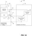
- FIG. 1A is a block diagram of an illustrative example of an electronic device 100 not covered by the subject-matter of the claims including a particular example of a power manager integrated circuit (PMIC) 102 and an integrated circuit device 104.
- the integrated circuit device 104 may include multiple power domains, such as a first power domain 106 and a second power domain 108.
- the power manager integrated circuit 102 may include a switching regulator 110, logic 112, a transistor (switch) 114, a first pin 116 and a second pin 118.
- the switching regulator 110 is coupled to the first pin 116 and is coupled to the second pin 118 via the switch 114.
- the switch 114 may be a metal oxide semiconductor field effect transistor (MOSFET), a field effect transistor (FET), a bipolar junction transistor, or another circuit device that may be controlled by logic 112 to selectively enable and disable current flow to the second pin 118.
- MOSFET metal oxide semiconductor field effect transistor
- FET field effect transistor
- bipolar junction transistor or another circuit device that may be controlled by logic 112 to selectively enable and disable current flow to the second pin 118.
- the switch 114 may be an n-channel MOSFET or a p-channel MOSFET device in the PMIC technology. If the switch 114 is an n-channel MOSFET device, then the switching regulator 110 may be at a larger voltage potential than the integrated circuit device 104.
- the switch 114 includes a first terminal 120 coupled to the first pin 116, a control terminal 122 coupled to the logic 112, and a second terminal 124 coupled to the second pin 118.
- the first pin 116 may be coupled to the first power domain 106 of the integrated circuit device 104
- the second pin 118 may be coupled to the second power domain 108 of the integrated circuit device 104.
- a third pin 126 may provide a ground connection to the PMIC 102 for the first power domain and the second power domain.
- the switching regulator 110 provides a regulated power supply to the first pin 116.
- the logic 112 may activate the switch 114 via the control terminal 122 to provide at least a portion of the regulated power supply to the second pin 118.
- the logic 112 may selectively deactivate the switch 114 to substantially reduce current flow to the second pin 118.
- the switching regulator 110 may continue to deliver power to the first pin 116 and to the first power domain 106 after current flow to the second pin 118 is reduced.
- the switching regulator 110 may be utilized to selectively provide power to the second power domain 108 of the integrated circuit device 104.
- random access memory such as synchronous dynamic random access memory (SDRAM) and other memory components account for a significant amount of static power consumption.
- SDRAM synchronous dynamic random access memory
- a 256 Mbit SDRAM such as that produced by Elpida Memory, Inc. of Japan
- An SDRAM that consumes 1.02pA per bit at 1.8 volts consumes approximately 1.84 picowatts per bit.
- the switching regulator 110 By utilizing a single switching regulator, such as the switching regulator 110, to produce the regulated power supply, it is possible to deliver a consistent power supply to one power domain, such as the first power domain 106, allowing state information to be retained in a memory location within the first power domain 106, while significantly reducing power to other power domains of the integrated circuit device 104, such as the second power domain 108.
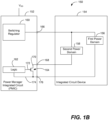
- FIG. 1B is a block diagram of an alternative illustrative example of an electronic device 150 not covered by the subject-matter of the claims including a particular example of a power manager integrated circuit (PMIC) 152 and an integrated circuit device 154.
- the electronic device 150 includes a PMIC 152 arranged in foot-switch configuration.
- the integrated circuit device 154 may include multiple power domains, such as the first power domain 156 and the second power domain 158.
- the power manager integrated circuit 152 may include a switching regulator 160, logic 162, a transistor (switch) 164, a first pin 166, a second pin 168, and a third pin 176.
- the switching regulator 160 is coupled to the first power domain 156 and the second power domain 158 via the first pin 166.
- the switch 164 includes a first terminal 170 that is coupled to the second power domain 158 via the second pin 168.
- the switch 164 also includes a control terminal 172 that is coupled to the logic 162 and a second terminal 174 coupled to the logic 162 and to the third pin 176.
- the first power domain 156 may be coupled to the logic 162 via the third pin 176.
- the PMIC 152 may selectively disable the second power domain 158 by deactivating the switch 164 to reduce current flow, while providing power to the first power domain 156 via the switching regulator 160.
- the PMIC 102 and the PMIC 152 of FIGS. 1A and 1B may include more than one switch 114 and that the integrated circuit device 104 may include a plurality of power domains.
- the switches may be selectively deactivated to disable power to selected power domains of a plurality of power domains of the integrated circuit device 104.
- FIG. 2 is a diagram of an illustrative portion 200 of a particular example of a power manager integrated circuit (PMIC) 102 not covered by the subject-matter of the claims.
- the PMIC 102 includes a switching regulator, such as the switching regulator 110 and logic 112.
- the switching regulator 110 may include a buck controller 204, a first transistor 206, and a second transistor 208.
- the logic 112 may include a head controller 210.
- the PMIC 102 may also include a third transistor 212, a first pin 116, a second pin 118, a third pin 214 and a fourth pin 218.
- the fourth pin 218 may be coupled to a power supply terminal, such as V DD in FIG. 1A .
- the first transistor 206 includes a first terminal 220 coupled to the fourth pin 218, a control terminal 222 coupled to the buck regulator 204, and a second terminal 224 coupled to the third pin 214.
- the second transistor 208 includes a first terminal 226 coupled to the third pin 214, a control terminal 228 coupled to the buck controller 204, and a second terminal 230 coupled to a voltage supply terminal, which may be an electrical ground.
- the third transistor 212 includes a first terminal 232 coupled to the first pin 116, a control terminal 234 coupled to the head controller 210, and a second terminal 236 coupled to the second pin 118.
- An external inductor 238 may be coupled between the third pin 214 and the first pin 116.
- a capacitor 240 may be coupled between the first pin 116 and a voltage supply terminal, which may be an electrical ground, to filter the power supply to the first power domain.
- a capacitor 242 may be coupled between the second pin 118 and a voltage supply terminal, which may be an electrical ground, to filter the power supply to the second power domain.
- the switching regulator 110 is coupled to the first pin 116 to provide a first regulated power supply to the first power domain and is coupled to the second pin 118 to provide a second regulated power supply to the second power domain via the third transistor 212.
- the head controller 210 is coupled to the control terminal 234 of the third transistor 212 and to the second pin 118 to selectively deactivate the third transistor 212, such as during a low power event.
- the third transistor 212 may be a high voltage transistor and may operate as a switch to selectively deactivate a second regulated power supply to the second power domain.
- the head controller 210 may selectively activate the third transistor 212 to provide current flow to the second pin 118 during a normal operating mode.
- the head controller 210 may selectively deactivate the third transistor 212 to substantially reduce or shut off current flow to the second pin 118 during a low power event, such as a shut down event, an idle event, a reduced power event, or any combination thereof.
- the head controller 210 may operate to substantially reduce leakage current via the third transistor 212, for example, to a current level less than approximately 100 nanoamperes.
- the third transistor 212 cooperates with the head controller 210 to use the regulated voltage supply provided by the buck regulator (e.g. the buck controller 204, the first transistor 206 and the second transistor 208) to provide a switched power supply to the second pin 118 without using extra components, such as extra voltage regulators.
- the first pin 116 receives a regulated output from the buck regulator 204, and the second pin 116 receives an unregulated output generated from the regulated output via the third transistor (head switch) 212.
- the third transistor 212 can be designed to provide a voltage drop of approximately 5mV when a 100mA load is coupled to the second pin 118.
- a circuit design process typically includes establishing and maintaining correct circuit behavior under a variety of operating conditions, including variations in process, voltage, and temperature (PVT). Therefore, behavioral modeling of analog circuits typically includes extending the integrated circuit model to accurately represent the behavior of the integrated circuit at possible PVT values.
- the third transistor 212 should be designed to have an on-resistance that is small enough to maintain consistent performance at the PVT values.
- the output voltage specification specifies a medium voltage n-channel field effect transistor (NFET) for the third transistor 212.
- NFET medium voltage n-channel field effect transistor
- the estimated wafer price of approximately 2.4 cents per square millimeter indicates that the silicon cost is 1.2 cents for the third switch 212.
- the PMIC 102 and an associated integrated circuit that includes multiple power domains may be manufactured using different semiconductor manufacturing technologies.
- the PMIC 102 may be fabricated using a 0.18nm high voltage CMOS process, while the integrated circuit device 104 may be manufactured using a 45nm process.
- the PMIC 102 may be fabricated using a 45nm technology and the integrated circuit device may be fabricated using a 100nm technology (e.g. the PMIC 102 may be fabricated using an older fabrication technology, while the integrated circuit device, such as the integrated circuit device 104 of FIG. 1A , may be fabricated using a newer fabrication technology).
- FIG. 3 is a diagram of a portion 300 of a particular illustrative example of the power manager integrated circuit (PMIC) 102 of FIG. 2 not covered by the subject-matter of the claims.
- the PMIC 102 may include the switching regulator 110, the logic 112, and other elements of the portion 200 of FIG. 2 , as well as a fourth transistor 302 arranged in parallel with the third transistor 212.
- the fourth transistor 302 may include a first terminal 304 coupled to the first pin 116, a control terminal 306 coupled to the control terminal 234 of the third transistor 212, and a second terminal 306 coupled to the second pin 118.
- the fourth transistor 302 may reduce a voltage drop across the third transistor 212 during normal operation, in part, by dividing current flow between the third transistor 212 and the fourth transistor 214. Moreover, by activating the third transistor 212 and the fourth transistor 302, more current may flow to the second pin 118 than would otherwise be possible without exceeding a current rating of the third transistor 212. During a low-power or shut down event, the head controller 210 may deactivate the third transistor 212 and the fourth transistor 302 to turn off current flow to the second pin 118, and to reduce leakage. In a particular example, the leakage current may be reduced to a level that is less than approximately 100 nanoamperes.
- FIG. 4 is an illustrative diagram of a particular illustrative embodiment of a portion 400 of a particular embodiment of a power manager integrated circuit (PMIC) 102.
- the PMIC 102 includes the switching regulator 110 and the logic 112.
- the logic 112 includes a first low dropout regulator 402 and a second low dropout regulator 404.
- a low dropout regulator may include a voltage regulator that provides a regulated voltage supply with a low voltage drop (e.g. low power consumption).
- the line 406 couples the low dropout regulators 402 and 404 to the first pin 116.
- the first low dropout regulator 402 is coupled to the second pin 118 to provide a second regulated power supply derived from the first regulated power supply provided to the first pin 116 by the switching regulator 110, and the second low dropout regulator 404 is coupled to a fifth pin 408.
- the first pin 116 may be coupled to a first power domain of a circuit device (such as the integrated circuit device 104 of FIG. 1A ) to provide a first regulated power supply to the first power domain.
- the second pin 118 may be coupled to a second power domain of the circuit device to provide a second regulated power supply to the second power domain.
- the fifth pin 408 may be coupled to a third power domain of a circuit device to provide a third regulated power supply to the third power domain.
- the logic 112 may include multiple low dropout regulators and may be adapted to selectively control each of the low dropout regulators to activate and deactivate a regulated power supply to an associated power domain of the integrated circuit.
- a capacitor 410 may be coupled between the fifth pin 408 and a voltage supply terminal, which may be an electrical ground, to filter the power supply to the third power domain.
- the switching regulator 110 provides the first regulated power supply to the first pin 116 and the low dropout regulators 402 and 404 generate second and third regulated power supplies, respectively, based on the first regulated power supply.
- the low dropout regulators 402 and 404 can be designed to provide power supplies that are approximately matched supplies (such as within 5mV of each other).
- the first low dropout (LDO) regulator 402 may be approximately a 300mA LDO regulator and the second LDO regulator 404 may be approximately a 150mA LDO regulator.
- the layout area of the first LDO regulator 402 and the second LDO regulator 404 may be estimated to be approximately 0.17mm 2 and 0.11mm 2 , respectively.
- the total silicon cost of the two LDO regulators 402 and 404 may be approximately 0.67 cents.
- the switching regulator 110 may be a high voltage power regulator.
- the LDO regulators 402 and 404 may be lower voltage regulators, which are adapted to derive power from the switching regulator 110.
- the LDO regulators 402 and 404 may be produced using less silicon area than the switching regulator 110.
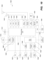
- FIG. 5 is a block diagram of a system 500 including an integrated circuit device 104 having a plurality of power domains and including a power manager integrated circuit 102 according to FIGS. 1-4 .
- the integrated circuit device 104 may include a plurality of power domains, including a Vcizi power domain 502, a distributed power domain 504, a V C1Z3 power domain 506, a distributed power domain 508, a Vcci power domain 510, distributed power domains 512 and 514, a V C1Z2 power domain 516, a V C2Z1 power domain 518, and a V CC2 power domain 520.
- the power manager integrated circuit (PMIC) 102 may be adapted to provide one or more regulated power supplies to one or more of the power domains, using a single switching regulator, as shown in FIGS. 1-4 .
- the PMIC 102 may provide a first regulated power supply V REG , for example, to the Vcizi power domain 502 via line 522.
- the PMIC 102 may also provide a second power supply (Vz) to the V C1Z2 power domain 516 via line 524, a third power supply (V 3 ) to the V C2Z1 power domain 518 via line 526, and a fourth power supply (V 4 ) to the V C1Z3 power domain 506 via line 528.
- the second, third and fourth power supplies may be unregulated if the PMIC 102 includes the particular arrangement of FIGS. 1-3 or may be regulated if the PMIC 102 includes the particular arrangement of FIG. 4 .
- FIG. 6 is a flow diagram of a method of selectively disabling or substantially reducing current flow to at least one pin of a power manager integrated circuit of a system.
- a power supply may be received from a voltage supply terminal at a power manager integrated circuit (block 600).
- a first regulated supply voltage is supplied to a first pin of the power manager integrated circuit (block 602).
- a current flow is selectively enabled to the second pin, where the second pin is coupled to a second power domain of the integrated circuit device including a first power domain responsive to the first pin and the second power domain responsive to the second pin (block 606).
- the current flow may be selectively enabled by activating a transistor (such as the third transistor 212 of FIGS.
- the current flow may be selectively disabled to the second pin, for example, when the system is in a low power or a power off mode of operation (block 608).
- the voltage level may optionally be scaled to one of the first power domain or the second power domain (block 610).
- logic of the PMIC (such as logic 112 in FIG. 1A ) may operate to scale a voltage level to one or more power domains of the integrated circuit device, to scale or adjust a power supply to a collapsible power domain, for example.
- the current flow may be selectively disabled by deactivating one or more transistors (e.g. the third transistor 212 and the fourth transistor 302 of FIG. 3 ) to substantially reduce current flow to the second pin (such as the second pin 118 of FIGS. 1-4 ).
- the current flow to the second pin may be reduced to a current level that is less than approximately 100 nanoamperes, thereby reducing power to the second power domain.
- the method may include providing the regulated power supply to the first pin to provide power to the first power domain, which may include a memory, during the low power mode to retain a state of the integrated circuit device.
- the first regulated power supply and the second regulated power supply may be at different power levels.
- the power manager integrated circuit may provide a different regulated power supply to each domain of a plurality of power domains of the integrated circuit, and each of the power supplies may be selectively deactivated.
- FIG. 7 illustrates an exemplary, non-limiting embodiment of a portable communication device that is generally designated 700.
- the portable communication device includes an on-chip system 722 that includes a processing unit 710, which may be a general purpose processor, a digital signal processor, an advanced reduced instruction set machine processor, or any combination thereof.
- FIG. 7 also shows a display controller 726 that is coupled to the processing unit 710 and a display 728.
- an input device 730 is coupled to the processing unit 710.
- a memory 732 is coupled to the processing unit 710.
- a coder/decoder (CODEC) 734 can be coupled to the processing unit 710.
- a speaker 736 and a microphone 738 can be coupled to the CODEC 730.
- CODEC coder/decoder
- the processing unit 710, the display controller 726, the memory 732, the CODEC 734, other components, or any combination thereof may receive power via one or more pins of a power manager integrated circuit (PMIC) 757, as shown in FIGS. 1-6 and described herein.
- PMIC power manager integrated circuit
- FIG. 7 also indicates that a wireless controller 740 can be coupled to the processing unit 710 and a wireless antenna 742.
- a power supply 744 is coupled to the on-chip system 722.
- the display 728, the input device 730, the speaker 736, the microphone 738, the wireless antenna 742, and the power supply 744 are external to the on-chip system 722. However, each is coupled to a component of the on-chip system 722.
- the PMIC 757 may be coupled to the power supply 744 to receive an unregulated power supply, which the PMIC 757 may utilize to generate the regulated power supply and to selectively activate power to one or more power domains of an integrated circuit device, which may include one or more elements (such as the processing unit 710, the wireless controller 740, the memory 732, the display controller 726 and the CODEC 734).
- an integrated circuit device which may include one or more elements (such as the processing unit 710, the wireless controller 740, the memory 732, the display controller 726 and the CODEC 734).
- the processing unit 710 may process instructions associated with programs necessary to perform the functionality and operations needed by the various components of the portable communication device 700. For example, when a wireless communication session is established via the wireless antenna a user can speak into the microphone 738. Electronic signals representing the user's voice can be sent to the CODEC 734 to be encoded. The processing unit 710 can perform data processing for the CODEC 734 to encode the electronic signals from the microphone. Further, incoming signals received via the wireless antenna 742 can be sent to the CODEC 734 by the wireless controller 740 to be decoded and sent to the speaker 736. The processing unit 710 can also perform the data processing for the CODEC 734 when decoding the signal received via the wireless antenna 742.
- the processing unit 710 can process inputs that are received from the input device 730. For example, during the wireless communication session, a user may be using the input device 730 and the display 728 to surf the Internet via a web browser that is embedded within the memory 732 of the portable communication device 700.
- the wireless telephone 800 includes an on-chip system 822 that includes a digital baseband processor 810 and an analog baseband processor 826 that are coupled together.
- the wireless telephone 800 may alternatively include a general-purpose processor that is adapted to execute processor readable instructions to perform digital or analog signal processing, as well as other operations.
- a general-purpose processor (not shown) may be included in addition to the digital baseband processor 810 and the analog baseband processor 826 to execute processor readable instructions.
- a display controller 828 and a touchscreen controller 830 are coupled to the digital baseband processor 810.
- a touchscreen display 832 external to the on-chip system 822 is coupled to the display controller 828 and to the touchscreen controller 830.
- the digital baseband processor 810, the analog baseband processor 826, the display controller 828, the touchscreen controller 830, other components, or any combination thereof may receive power from a power manager integrated circuit (PMIC) 857, such as the PMIC devices shown in FIGS. 1-6 and described herein.
- PMIC power manager integrated circuit
- FIG. 8 further indicates that a video encoder 834, e.g., a phase alternating line (PAL) encoder, a sequential fashion Malawi memoire (SECAM) encoder, or a national television system(s) committee (NTSC) encoder, is coupled to the digital baseband processor 810.
- a video amplifier 836 is coupled to the video encoder 834 and to the touchscreen display 832.
- a video port 838 is coupled to the video amplifier 836.
- a universal serial bus (USB) controller 840 is coupled to the digital baseband processor 810.
- a USB port 842 is coupled to the USB controller 840.
- USB universal serial bus
- a memory 844 and a subscriber identity module (SIM) card 846 can also be coupled to the digital baseband processor 810. Further, as shown in FIG. 8 , a digital camera 848 can be coupled to the digital baseband processor 810. In an exemplary embodiment, the digital camera 848 is a charge-coupled device (CCD) camera or a complementary metal-oxide semiconductor (CMOS) camera.
- CCD charge-coupled device
- CMOS complementary metal-oxide semiconductor
- a stereo audio CODEC 850 can be coupled to the analog baseband processor 826.
- an audio amplifier 852 can coupled to the to the stereo audio CODEC 880.
- a first stereo speaker 854 and a second stereo speaker 856 are coupled to the audio amplifier 852.
- FIG. 8 shows that a microphone amplifier 858 can be also coupled to the stereo audio CODEC 850.
- a microphone 860 can be coupled to the microphone amplifier 858.
- a frequency modulation (FM) radio tuner 862 can be coupled to the stereo audio CODEC 850.
- an FM antenna 864 is coupled to the FM radio tuner 862.
- stereo headphones 866 can be coupled to the stereo audio CODEC 850.
- FM frequency modulation
- FIG. 8 further indicates that a radio frequency (RF) transceiver 868 can be coupled to the analog baseband processor 826.
- An RF switch 870 can be coupled to the RF transceiver 868 and to an RF antenna 872.
- a keypad 874 can be coupled to the analog baseband processor 826.
- a mono headset with a microphone 876 can be coupled to the analog baseband processor 826.
- a vibrator device 878 can be coupled to the analog baseband processor 826.
- FIG. 8 also shows that a power supply 880 can be coupled to the on-chip system 822.
- the power supply 880 is a direct current (DC) power supply that provides power to the various components of the wireless telephone 800 that require power.
- DC direct current
- the power supply is a rechargeable DC battery or a DC power supply that is derived from an alternating current (AC) to DC transformer that is connected to an AC power source.
- the PMIC 857 may be coupled to the power supply 880 to receive an unregulated power supply, which the PMIC 857 may utilize to generate a regulated power supply.
- the PMIC 857 may provide the regulated power supply to one or more power domains of an integrated circuit device, which may include one or more elements (such as the display controller 828, the digital signal processor 810, the USB controller 840, the touchscreen controller 830, the video amplifier 836, the PAL/SECAM/NTSC encoder 834, the memory 844, the SIM card 846, the audio amplifier 852, the microphone amplifier 858, the FM radio tuner 862, the stereo audio CODEC 850, the analog baseband processor 826, and the RF transceiver 868).
- a power domain of the integrated circuit device may include one or more of the elements.
- the power control unit 857 may selectively activate power to one or more of the power domains, as described above with respect to FIGS. 1-6 .
- the touchscreen display 832, the video port 838, the USB port 842, the camera 848, the first stereo speaker 854, the second stereo speaker 856, the microphone 860, the FM antenna 864, the stereo headphones 866, the RF switch 870, the RF antenna 872, the keypad 874, the mono headset 876, the vibrator 878, and the power supply 880 are external to the on-chip system 822.
- the wireless IP telephone 900 includes an on-chip system 902 that includes a processing unit 904.
- the processing unit 904 may be a digital signal processor, a general purpose processor, an advanced reduced instruction set computing machine processor, an analog signal processor, a processor to execute processor readable instruction sets, or any combination thereof.
- a display controller 906 is coupled to the processing unit 904 and a display 908 is coupled to the display controller 906.
- the display 908 is a liquid crystal display (LCD).
- a keypad 910 can be coupled to the processing unit 904.
- the processing unit 904, the display controller 906, other components, or any combination thereof may receive power via a power manager integrated circuit (PMIC) 957, such as that shown in FIGS. 1-6 and described herein.
- PMIC power manager integrated circuit
- a flash memory 912 can be coupled to the processing unit 904.
- a synchronous dynamic random access memory (SDRAM) 914, a static random access memory (SRAM) 916, and an electrically erasable programmable read only memory (EEPROM) 918 can also be coupled to the processing unit 904.
- FIG. 9 also shows that a light emitting diode (LED) 920 can be coupled to the processing unit 904.
- a voice CODEC 922 can be coupled to the processing unit 904.
- An amplifier 924 can be coupled to the voice CODEC 922 and a mono speaker 926 can be coupled to the amplifier 924.
- FIG. 9 further indicates that a mono headset 928 can also be coupled to the voice CODEC 922.
- the mono headset 928 includes a microphone.
- FIG. 9 also illustrates that a wireless local area network (WLAN) baseband processor 930 can be coupled to the processing unit 904.
- An RF transceiver 932 can be coupled to the WLAN baseband processor 930 and an RF antenna 934 can be coupled to the RF transceiver 932.
- a Bluetooth controller 936 can also be coupled to the processing unit 904 and a Bluetooth antenna 938 can be coupled to the controller 936.
- a USB port 940 may be coupled to the processing unit 904.
- a power supply 942 is coupled to the on-chip system 902 and provides power to the various components of the wireless IP telephone 900 via the PMIC 957.
- the display 908, the keypad 910, the LED 920, the mono speaker 926, the mono headset 928, the RF antenna 934, the Bluetooth antenna 938, the USB port 940, and the power supply 942 are external to the on-chip system 902.
- each of these components is coupled to one or more components of the on-chip system 902.
- the wireless VoIP device 900 includes the PMIC 957, which may be coupled to the power supply 942 to receive an unregulated power supply, which the PMIC 957 may utilize to generate the regulated power supply.
- the PMIC 957 may selectively provide the regulated power supply to one or more of the plurality of power domains of the on-chip system.
- a power domain of the on-chip system 902 may include one or more elements, such as the display controller 906, the amplifier 924, the voice CODEC 922, the processing unit 904, the flash memory 912, the SDRAM 914, the SRAM 916, the EEPROM 918, the RF transceiver 932, WLAN MAC baseband processor 930, and the Bluetooth controller 936.
- the power control unit 957 may selectively activate power to one or more of the power domains, as described above with respect to FIGS. 1-6 .
- FIG. 10 illustrates an exemplary, non-limiting embodiment of a portable digital assistant (PDA) that is generally designated 1000.
- the PDA 1000 includes an on-chip system 1002 that includes a processing unit 1004.
- a touchscreen controller 1006 and a display controller 1008 are coupled to the processing unit 1004.
- a touchscreen display 1010 is coupled to the touchscreen controller 1006 and to the display controller 1008.
- FIG. 10 also indicates that a keypad 1012 can be coupled to the processing unit 1004.
- the processing unit 1004, the touchscreen controller 1006, the display controller 1008, other components, or any combination thereof may receive power via a power manager integrated circuit (PMIC) 1057, as shown in FIGS. 1-6 and described herein.
- PMIC power manager integrated circuit
- a flash memory 1014 can be coupled to the processing unit 1004.
- the processing unit 1004 may be a digital signal processor (DSP), a general purpose processor, an advanced reduced instruction set computing machine, an analog signal processor, a processor adapted to execute processor readable instruction sets, or any combination thereof.
- DSP digital signal processor
- ROM read only memory
- DRAM dynamic random access memory
- EEPROM electrically erasable programmable read only memory
- FIG. 10 also shows that an infrared data association (IrDA) port 1022 can be coupled to the processing unit 1004.
- IrDA infrared data association
- a digital camera 1024 can be coupled to the processing unit 1004.
- a stereo audio CODEC 1026 can be coupled to the processing unit 1004.
- a first stereo amplifier 1028 can be coupled to the stereo audio CODEC 1026 and a first stereo speaker 1030 can be coupled to the first stereo amplifier 1028.
- a microphone amplifier 1032 can be coupled to the stereo audio CODEC 1026 and a microphone 1034 can be coupled to the microphone amplifier 1032.
- FIG. 10 further shows that a second stereo amplifier 1036 can be coupled to the stereo audio CODEC 1026 and to a second stereo speaker 1038.
- stereo headphones 1040 can also be coupled to the stereo audio CODEC 1026.
- FIG. 10 also illustrates that an 802.11 controller 1042 can be coupled to the processing unit 1004 and an 802.11 antenna 1044 can be coupled to the 802.11 controller 1042.
- a Bluetooth controller 1046 can be coupled to the processing unit 1004 and a Bluetooth antenna 1048 can be coupled to the Bluetooth controller 1046.
- a USB controller 1050 can be coupled to the processing unit 1004 and a USB port 1052 can be coupled to the USB controller 1050.
- a smart card 1054 e.g., a multimedia card (MMC) or a secure digital card (SD) can be coupled to the processing unit 1004.
- a power supply 1056 may be coupled to the PMIC 1057 of the on-chip system 1002 to provide power to the various components of the PDA 1000.
- the display 1010, the keypad 1012, the IrDA port 1022, the digital camera 1024, the first stereo speaker 1030, the microphone 1034, the second stereo speaker 1038, the stereo headphones 1040, the 802.11 antenna 1044, the Bluetooth antenna 1048, the USB port 1052, and the power supply 1056 are external to the on-chip system 1002.
- each of these components is coupled to one or more components on the on-chip system 1002.
- the PMIC 1057 may be coupled to the power supply 1056 to receive an unregulated power supply, which the PMIC 1057 may utilize to generate the regulated power supply.
- the PMIC 1057 may provide power to one or more power domains of the on-chip system 1002, which may include one or more elements (such as the display controller 1008, the touchscreen controller 1006, the stereo amplifier 1028, the microphone amplifier 1032, the stereo amplifier 1036, the processing unit 1004, the stereo audio CODEC 1026, the flash memory 1014, the ROM 1016, the DRAM 1018, the EEPROM 1020, the 802.11 controller 1042, the Bluetooth controller 1046, the USB controller 1050, and the smart card MMC SD 1054).
- a power domain of the on-chip system 1002 may include one or more of these elements, and the power control unit 1057 may selectively activate power to one or more of the power domains, as described above with respect to FIGS. 1-6 .
- a software module may reside in RAM memory, flash memory, ROM memory, PROM memory, EPROM memory, EEPROM memory, registers, hard disk, a removable disk, a CD-ROM, or any other form of storage medium known in the art.
- An exemplary storage medium may be coupled to the processor such that the processor can read information from, and write information to, the storage medium.
- the storage medium may be integral to the processor.
- the processor and the storage medium may reside in an ASIC.
- the ASIC may reside in a computing device or a user terminal.
- the processor and the storage medium may reside as discrete components in a computing device or user terminal.
Landscapes
- Engineering & Computer Science (AREA)
- Computer Hardware Design (AREA)
- Physics & Mathematics (AREA)
- Computing Systems (AREA)
- General Engineering & Computer Science (AREA)
- Mathematical Physics (AREA)
- Power Engineering (AREA)
- Semiconductor Integrated Circuits (AREA)
- Power Sources (AREA)
- Charge And Discharge Circuits For Batteries Or The Like (AREA)
- Dc-Dc Converters (AREA)
Claims (15)
- Eine integrierte Schaltung zum Energiemanagement (102), aufweisend:eine Abwärtssteuerung (204) zum Erzeugen einer ersten geregelten Stromversorgung;einen ersten Anschlussstift (116), der mit einer ersten Leistungsdomäne (106) einer integrierten Schaltung (104) gekoppelt ist und auf die Abwärtssteuerung (204) anspricht, um die erste geregelte Stromversorgung für die erste Leistungsdomäne (106) bereitzustellen;einen zweiten Anschlussstift (118), der mit einer zweiten Leistungsdomäne (108) der integrierten Schaltung (104) verbunden ist, um eine zweite geregelte Stromversorgung bereitzustellen, die von der ersten geregelten Stromversorgung abgeleitet ist, für die zweite Leistungsdomäne (108); undeine Kopfsteuerung (210) zum Bestimmen eines Betriebsmodus und zum selektiven Reduzieren oder Deaktivieren des Stromflusses zum zweiten Anschlussstift (118), wenn der Betriebsmodus einen Niedrigenergiemodus aufweist, wobei die Kopfsteuerung (210) aufweist:eine Logik (112, 132) zum Bestimmen des Betriebsmodus und zum Bereitstellen zumindest eines Steuersignals; undeinen Regler mit niedrigem Spannungsabfall (402), der einen mit dem ersten Anschlussstift (116) verbundenen Eingang und einen mit dem zweiten Anschlussstift (118) verbundenen Ausgang aufweist, wobei der Regler mit niedrigem Spannungsabfall (402) auf die Logik (112, 132) reagiert, um den Stromfluss zum zweiten Anschlussstift (118) selektiv zu reduzieren.
- Die integrierte Schaltung zum Energiemanagement (102) nach Anspruch 1, weiter aufweisend:einen dritten Anschlussstift, der mit einer externen Induktivität verbunden ist;einen ersten Transistor, der einen ersten Anschluss, der mit einem ersten Spannungsversorgungsanschluss verbunden ist, einen Steueranschluss, der mit der Abwärtssteuerung (204) verbunden ist, und einen zweiten Anschluss, der mit dem dritten Anschlussstift verbunden ist, aufweist;einen zweiten Transistor, der einen ersten Anschluss, der mit dem dritten Anschlussstift verbunden ist, einen Steueranschluss, der mit der Abwärtssteuerung (204) verbunden ist, und einen zweiten Anschluss aufweist, der mit einem zweiten Spannungsversorgungsanschluss verbunden ist;wobei der erste Transistor und der zweite Transistor auf der Abwärtssteuerung (204) ansprechen, um eine Stromversorgung für die Induktivität über den dritten Anschluss bereitzustellen.
- Die integrierte Schaltung zum Energiemanagement (102) nach Anspruch 1, die weiter Folgendes aufweist:
einen dritten Transistor mit einem ersten Anschluss, der mit dem ersten Anschlussstift (116) gekoppelt ist, einem Steueranschluss, der mit der Kopfsteuerung (210) gekoppelt ist, und einem zweiten Anschluss, der mit dem zweiten Anschlussstift (118) gekoppelt ist, wobei der dritte Transistor auf die Kopfsteuerung (210) reagiert, um den Stromfluss zum zweiten Anschlussstift (118) im Energiesparmodus selektiv zu reduzieren. - Die integrierte Schaltung zum Energiemanagement (102) nach Anspruch 3, weiter aufweisend:
einen vierten Transistor mit einem ersten Anschluss, der mit dem ersten Anschlussstift (116) gekoppelt ist, einem Steueranschluss, der mit dem Steueranschluss des dritten Transistors gekoppelt ist, und einem zweiten Anschluss, der mit dem zweiten Anschlussstift (118) gekoppelt ist, wobei der vierte Transistor auf die Kopfsteuerung anspricht, um den Stromfluss zum zweiten Anschlussstift (118) selektiv zu reduzieren. - Die integrierte Schaltung zum Energiemanagement (102) nach Anspruch 4, wobei die Kopfsteuerung (210) den Stromfluss zum zweiten Anschlussstift (118) auf einen Strompegel reduziert, der weniger als etwa 100 Nanoampere beträgt.
- Die integrierte Schaltung zum Energiemanagement (102) nach Anspruch 1, wobei die Abwärtssteuerung (204) eine erste geregelte Stromversorgung für die erste Leistungsdomäne (106) über den ersten Anschlussstift (116) bereitstellt und selektiv eine zweite geregelte Stromversorgung für die zweite Leistungsdomäne (108) über den zweiten Anschlussstift (118) bereitstellt.
- Die integrierte Schaltung zum Energiemanagement (102) nach Anspruch 1, wobei der integrierte Schaltkreis (102) eine Vielzahl von Leistungsdomänen umfasst und wobei die Abwärtssteuerung (204) so angepasst ist, dass diese die erste geregelte Stromversorgung für die erste Leistungsdomäne (106) über den ersten Anschlussstift (116) bereitzustellen, und die Kopfsteuerung (210) angepasst ist, die zweite geregelte Stromversorgung für die zweite Leistungsdomäne (108) und zumindest eine zusätzliche geregelte Stromversorgung für eine oder mehrere andere Leistungsdomänen der Vielzahl von Leistungsdomänen bereitzustellen.
- Die integrierte Schaltung zum Energiemanagement (102)nach Anspruch 1, wobei die Kopfsteuerung (210) angepasst ist, um zumindest einen Strompegel oder einen Spannungspegel an den zweiten Anschlussstift (118) anzupassen, um eine Stromversorgung der zweiten Leistungsdomäne (108) zu steuern.
- Ein Verfahren aufweisend:Bereitstellen (602) einer ersten geregelten Versorgungsspannung an einem ersten Anschlussstift (116) einer integrierten Schaltung zum Energiemanagement (102) und einer zweiten geregelten Versorgungsspannung an einem zweiten Anschlussstift (118) der integrierten Schaltung zum Energiemanagement (102) durch eine Abwärtssteuerung (204), wobei die zweite geregelte Versorgungsspannung von der ersten geregelten Versorgungsspannung abgeleitet wird;Bestimmen eines Betriebsmodus eines Reglers mit niedrigem Spannungsabfall (402) durch eine Logik (112,132) und Bereitstellen zumindest eines Steuersignals durch die Logik (112, 132); undselektives Reduzieren des Stromflusses zum zweiten Anschlussstift (118) durch den Regler mit niedrigem Spannungsabfall (402), der auf die Logik (112, 132) anspricht und einen mit dem ersten Anschlussstift (116) verbundenen Eingang und einen mit dem zweiten Anschlussstift (118) verbundenen Ausgang umfasst, gemäß dem Betriebsmodus des Reglers mit niedrigem Spannungsabfall (402) und dem Steuersignal, wenn der Betriebsmodus einen Niedrigenergiemodus aufweist, wobei die integrierte Schaltung zum Energiemanagement (102) mit einem integrierten Schaltkreisgerät (104) gekoppelt ist, das eine erste Leistungsdomäne (106), die auf den ersten Anschlussstift (116) anspricht, und eine zweite Leistungsdomäne (108), die auf den zweiten Anschlussstift (118) anspricht, aufweist.
- Das Verfahren nach Anspruch 9, wobei das selektive Reduzieren des Stromflusses aufweist:
Deaktivieren eines Transistors, der mit dem ersten Anschlussstift (116) und dem zweiten Anschlussstift (118) gekoppelt ist, um den Stromfluss zu dem zweiten Anschlussstift (118) in einem Niedrigleistungsmodus wesentlich zu reduzieren. - Das Verfahren nach Anspruch 9, wobei die erste geregelte Stromversorgung auf einem anderen Leistungspegel als die zweite geregelte Stromversorgung ist.
- Das Verfahren nach Anspruch 9, wobei das selektive Reduzieren des Stromflusses das Reduzieren des Stromflusses zu dem zweiten Anschlussstift (118) auf einen Strompegel aufweist, der geringer als ungefähr 100 Nanoampere ist.
- Das Verfahren nach Anspruch 9, weiter aufweisend:
Skalieren (610) eines Spannungspegels auf die zweite Leistungsdomäne (108), um einen Leistungspegel der zweiten Leistungsdomäne (108) über einen Zeitraum einzustellen. - Ein System, aufweisend:eine integrierte Schaltung zum Energiemanagement (102) gemäß einem der Ansprüche 1 bis 8; undein integriertes Schaltungsgerät (104), aufweisend eine erste Leistungsdomäne (106), die auf den ersten Anschlussstift (116) anspricht, und eine zweite Leistungsdomäne (108), die auf den zweiten Anschlussstift (118) anspricht.
- Ein mobiles Kommunikationsgerät (800, 900, 1000), aufweisend:ein integriertes Schaltungsgerät (104) beinhaltend eine Vielzahl von Leistungsdomänen (106, 108); undeine integrierte Schaltung zum Energiemanagement (102) gemäß einem der Ansprüche 1 bis 8.
Applications Claiming Priority (4)
| Application Number | Priority Date | Filing Date | Title |
|---|---|---|---|
| US11/431,790 US7902654B2 (en) | 2006-05-10 | 2006-05-10 | System and method of silicon switched power delivery using a package |
| US11/532,000 US7812582B2 (en) | 2006-09-14 | 2006-09-14 | System and method of power distribution control of an integrated circuit |
| PCT/US2007/067227 WO2007133899A1 (en) | 2006-05-10 | 2007-04-23 | System and method of power distribution control of an integrated circuit |
| EP07761131.7A EP2025059B1 (de) | 2006-05-10 | 2007-04-23 | System und verfahren zur energieverteilungssteuerung einer integrierten schaltung |
Related Parent Applications (2)
| Application Number | Title | Priority Date | Filing Date |
|---|---|---|---|
| EP07761131.7A Division EP2025059B1 (de) | 2006-05-10 | 2007-04-23 | System und verfahren zur energieverteilungssteuerung einer integrierten schaltung |
| EP07761131.7A Division-Into EP2025059B1 (de) | 2006-05-10 | 2007-04-23 | System und verfahren zur energieverteilungssteuerung einer integrierten schaltung |
Publications (2)
| Publication Number | Publication Date |
|---|---|
| EP3694092A1 EP3694092A1 (de) | 2020-08-12 |
| EP3694092B1 true EP3694092B1 (de) | 2024-11-27 |
Family
ID=38472962
Family Applications (2)
| Application Number | Title | Priority Date | Filing Date |
|---|---|---|---|
| EP07761131.7A Active EP2025059B1 (de) | 2006-05-10 | 2007-04-23 | System und verfahren zur energieverteilungssteuerung einer integrierten schaltung |
| EP20166805.0A Active EP3694092B1 (de) | 2006-05-10 | 2007-04-23 | System und verfahren zur leistungsverteilungssteuerung einer integrierten schaltung |
Family Applications Before (1)
| Application Number | Title | Priority Date | Filing Date |
|---|---|---|---|
| EP07761131.7A Active EP2025059B1 (de) | 2006-05-10 | 2007-04-23 | System und verfahren zur energieverteilungssteuerung einer integrierten schaltung |
Country Status (6)
| Country | Link |
|---|---|
| EP (2) | EP2025059B1 (de) |
| JP (1) | JP4897877B2 (de) |
| KR (1) | KR101046112B1 (de) |
| CN (1) | CN103219985B (de) |
| ES (1) | ES2810015T3 (de) |
| WO (1) | WO2007133899A1 (de) |
Families Citing this family (9)
| Publication number | Priority date | Publication date | Assignee | Title |
|---|---|---|---|---|
| JP5182513B2 (ja) * | 2007-12-27 | 2013-04-17 | 株式会社リコー | 画像処理装置及びその省電力制御方法 |
| JP5374120B2 (ja) * | 2008-11-14 | 2013-12-25 | ルネサスエレクトロニクス株式会社 | 半導体集積回路装置 |
| US8564260B2 (en) * | 2010-12-17 | 2013-10-22 | Qualcomm Incorporated | Dual-stage power conversion |
| JP2013110337A (ja) * | 2011-11-24 | 2013-06-06 | Fujitsu Semiconductor Ltd | 半導体集積回路 |
| EP3157151B1 (de) * | 2014-06-10 | 2021-08-11 | Hitachi Automotive Systems, Ltd. | Elektronische steuerungsvorrichtung |
| KR102275497B1 (ko) * | 2014-10-20 | 2021-07-09 | 삼성전자주식회사 | 전원 경로 제어기를 포함하는 시스템 온 칩 및 전자 기기 |
| US10754413B2 (en) * | 2017-09-30 | 2020-08-25 | Intel Corporation | Mechanism to enter or exit retention level voltage while a system-on-a-chip is in low power mode |
| US12348061B2 (en) * | 2021-05-18 | 2025-07-01 | Intel Corporation | Power delivery architecture for high power portable devices |
| CN119696373A (zh) * | 2025-02-21 | 2025-03-25 | 荣耀终端股份有限公司 | 一种供电芯片、芯片及电子设备 |
Family Cites Families (14)
| Publication number | Priority date | Publication date | Assignee | Title |
|---|---|---|---|---|
| JPH10201135A (ja) * | 1997-01-14 | 1998-07-31 | Nec Home Electron Ltd | 電源回路 |
| JPH11306754A (ja) * | 1998-04-15 | 1999-11-05 | Nec Corp | 半導体集積回路 |
| JP2000013215A (ja) * | 1998-04-20 | 2000-01-14 | Nec Corp | 半導体集積回路 |
| JP2002116237A (ja) * | 2000-10-10 | 2002-04-19 | Texas Instr Japan Ltd | 半導体集積回路 |
| US6242896B1 (en) * | 2000-10-20 | 2001-06-05 | Hewlett-Packard Company | Converting available electrical power to desirable electrical power |
| JP3817446B2 (ja) * | 2001-02-15 | 2006-09-06 | 株式会社リコー | 電源回路及びdc−dcコンバータの出力電圧制御方法 |
| JP4910259B2 (ja) * | 2001-07-25 | 2012-04-04 | 日本テキサス・インスツルメンツ株式会社 | 半導体集積回路 |
| WO2003085501A1 (en) * | 2002-04-04 | 2003-10-16 | Matsushita Electric Industrial Co., Ltd. | Multiple power source semiconductor integrated circuit |
| JP3724472B2 (ja) * | 2002-10-16 | 2005-12-07 | ソニー株式会社 | 電子機器と電力供給方法 |
| US6879142B2 (en) * | 2003-08-20 | 2005-04-12 | Broadcom Corporation | Power management unit for use in portable applications |
| GB0324292D0 (en) * | 2003-10-17 | 2003-11-19 | Huggins Mark | Embedded power supplies particularly for large scale integrated circuits |
| JP4662235B2 (ja) * | 2004-07-14 | 2011-03-30 | 株式会社リコー | 論理シミュレーション装置およびその方法 |
| US20060061383A1 (en) * | 2004-08-31 | 2006-03-23 | Yihe Huang | On-chip power regulator for ultra low leakage current |
| JP2006217540A (ja) * | 2005-02-07 | 2006-08-17 | Fujitsu Ltd | 半導体集積回路および半導体集積回路の制御方法 |
-
2007
- 2007-04-23 JP JP2009509944A patent/JP4897877B2/ja active Active
- 2007-04-23 EP EP07761131.7A patent/EP2025059B1/de active Active
- 2007-04-23 EP EP20166805.0A patent/EP3694092B1/de active Active
- 2007-04-23 KR KR1020087030116A patent/KR101046112B1/ko active Active
- 2007-04-23 ES ES07761131T patent/ES2810015T3/es active Active
- 2007-04-23 CN CN201310162856.4A patent/CN103219985B/zh active Active
- 2007-04-23 WO PCT/US2007/067227 patent/WO2007133899A1/en not_active Ceased
Also Published As
| Publication number | Publication date |
|---|---|
| JP4897877B2 (ja) | 2012-03-14 |
| KR20090009317A (ko) | 2009-01-22 |
| WO2007133899A1 (en) | 2007-11-22 |
| CN103219985A (zh) | 2013-07-24 |
| JP2009536815A (ja) | 2009-10-15 |
| KR101046112B1 (ko) | 2011-07-01 |
| EP2025059A1 (de) | 2009-02-18 |
| CN103219985B (zh) | 2016-09-28 |
| ES2810015T3 (es) | 2021-03-08 |
| EP3694092A1 (de) | 2020-08-12 |
| EP2025059B1 (de) | 2020-05-06 |
Similar Documents
| Publication | Publication Date | Title |
|---|---|---|
| US7812582B2 (en) | System and method of power distribution control of an integrated circuit | |
| CN101438496B (zh) | 集成电路的功率分配控制的系统及方法 | |
| EP3694092B1 (de) | System und verfahren zur leistungsverteilungssteuerung einer integrierten schaltung | |
| US7279927B2 (en) | Integrated circuit with multiple power domains | |
| US9990022B2 (en) | Adaptive power multiplexing with a power distribution network | |
| US7049802B2 (en) | Power savings in a voltage supply controlled according to a work capability operating mode of an integrated circuit | |
| TWI506936B (zh) | 電壓調整器、用於切換式電壓調整器之設備及具有該調整器之系統 | |
| CN103430439B (zh) | Dc-dc转换器 | |
| JP2001211640A (ja) | 電子装置と半導体集積回路及び情報処理システム | |
| US20110197084A1 (en) | Power saving system and method employed in computer | |
| JP2011508582A (ja) | スイッチング回路を使用して、電力を提供するシステムと方法 | |
| CN106537714A (zh) | 基于电池电荷的动态睡眠模式 | |
| CN117707265B (zh) | 电子设备及电压调整芯片 | |
| US20230124949A1 (en) | True power shedding apparatus and method to reduce power consumption | |
| TWI877221B (zh) | 電源供應設備及電子系統 | |
| JP2004047810A (ja) | 半導体集積回路 | |
| JP2005045873A (ja) | 電源装置 | |
| US12093113B2 (en) | Communicating a desired power state to a power stage from a phase controller in a power supply | |
| CN106130127A (zh) | 电子设备及充电方法 | |
| JP3895994B2 (ja) | 半導体集積回路 | |
| RU2424586C2 (ru) | Система и способ для маломощной логики числовой шины в памяти |
Legal Events
| Date | Code | Title | Description |
|---|---|---|---|
| PUAI | Public reference made under article 153(3) epc to a published international application that has entered the european phase |
Free format text: ORIGINAL CODE: 0009012 |
|
| STAA | Information on the status of an ep patent application or granted ep patent |
Free format text: STATUS: REQUEST FOR EXAMINATION WAS MADE |
|
| 17P | Request for examination filed |
Effective date: 20200330 |
|
| AC | Divisional application: reference to earlier application |
Ref document number: 2025059 Country of ref document: EP Kind code of ref document: P |
|
| AK | Designated contracting states |
Kind code of ref document: A1 Designated state(s): AT BE BG CH CY CZ DE DK EE ES FI FR GB GR HU IE IS IT LI LT LU LV MC MT NL PL PT RO SE SI SK TR |
|
| STAA | Information on the status of an ep patent application or granted ep patent |
Free format text: STATUS: EXAMINATION IS IN PROGRESS |
|
| 17Q | First examination report despatched |
Effective date: 20230215 |
|
| GRAP | Despatch of communication of intention to grant a patent |
Free format text: ORIGINAL CODE: EPIDOSNIGR1 |
|
| STAA | Information on the status of an ep patent application or granted ep patent |
Free format text: STATUS: GRANT OF PATENT IS INTENDED |
|
| RIC1 | Information provided on ipc code assigned before grant |
Ipc: H02M 1/00 20060101ALN20240702BHEP Ipc: H03K 19/00 20060101ALI20240702BHEP Ipc: H02M 3/158 20060101AFI20240702BHEP |
|
| INTG | Intention to grant announced |
Effective date: 20240718 |
|
| GRAS | Grant fee paid |
Free format text: ORIGINAL CODE: EPIDOSNIGR3 |
|
| GRAA | (expected) grant |
Free format text: ORIGINAL CODE: 0009210 |
|
| STAA | Information on the status of an ep patent application or granted ep patent |
Free format text: STATUS: THE PATENT HAS BEEN GRANTED |
|
| AC | Divisional application: reference to earlier application |
Ref document number: 2025059 Country of ref document: EP Kind code of ref document: P |
|
| AK | Designated contracting states |
Kind code of ref document: B1 Designated state(s): AT BE BG CH CY CZ DE DK EE ES FI FR GB GR HU IE IS IT LI LT LU LV MC MT NL PL PT RO SE SI SK TR |
|
| REG | Reference to a national code |
Ref country code: GB Ref legal event code: FG4D |
|
| REG | Reference to a national code |
Ref country code: CH Ref legal event code: EP |
|
| REG | Reference to a national code |
Ref country code: IE Ref legal event code: FG4D |
|
| REG | Reference to a national code |
Ref country code: DE Ref legal event code: R096 Ref document number: 602007061943 Country of ref document: DE |
|
| REG | Reference to a national code |
Ref country code: LT Ref legal event code: MG9D |
|
| REG | Reference to a national code |
Ref country code: NL Ref legal event code: MP Effective date: 20241127 |
|
| PG25 | Lapsed in a contracting state [announced via postgrant information from national office to epo] |
Ref country code: PT Free format text: LAPSE BECAUSE OF FAILURE TO SUBMIT A TRANSLATION OF THE DESCRIPTION OR TO PAY THE FEE WITHIN THE PRESCRIBED TIME-LIMIT Effective date: 20250327 Ref country code: IS Free format text: LAPSE BECAUSE OF FAILURE TO SUBMIT A TRANSLATION OF THE DESCRIPTION OR TO PAY THE FEE WITHIN THE PRESCRIBED TIME-LIMIT Effective date: 20250327 |
|
| PG25 | Lapsed in a contracting state [announced via postgrant information from national office to epo] |
Ref country code: FI Free format text: LAPSE BECAUSE OF FAILURE TO SUBMIT A TRANSLATION OF THE DESCRIPTION OR TO PAY THE FEE WITHIN THE PRESCRIBED TIME-LIMIT Effective date: 20241127 Ref country code: NL Free format text: LAPSE BECAUSE OF FAILURE TO SUBMIT A TRANSLATION OF THE DESCRIPTION OR TO PAY THE FEE WITHIN THE PRESCRIBED TIME-LIMIT Effective date: 20241127 |
|
| REG | Reference to a national code |
Ref country code: AT Ref legal event code: MK05 Ref document number: 1746684 Country of ref document: AT Kind code of ref document: T Effective date: 20241127 |
|
| PG25 | Lapsed in a contracting state [announced via postgrant information from national office to epo] |
Ref country code: BG Free format text: LAPSE BECAUSE OF FAILURE TO SUBMIT A TRANSLATION OF THE DESCRIPTION OR TO PAY THE FEE WITHIN THE PRESCRIBED TIME-LIMIT Effective date: 20241127 |
|
| PG25 | Lapsed in a contracting state [announced via postgrant information from national office to epo] |
Ref country code: ES Free format text: LAPSE BECAUSE OF FAILURE TO SUBMIT A TRANSLATION OF THE DESCRIPTION OR TO PAY THE FEE WITHIN THE PRESCRIBED TIME-LIMIT Effective date: 20241127 |
|
| PG25 | Lapsed in a contracting state [announced via postgrant information from national office to epo] |
Ref country code: AT Free format text: LAPSE BECAUSE OF FAILURE TO SUBMIT A TRANSLATION OF THE DESCRIPTION OR TO PAY THE FEE WITHIN THE PRESCRIBED TIME-LIMIT Effective date: 20241127 Ref country code: LV Free format text: LAPSE BECAUSE OF FAILURE TO SUBMIT A TRANSLATION OF THE DESCRIPTION OR TO PAY THE FEE WITHIN THE PRESCRIBED TIME-LIMIT Effective date: 20241127 Ref country code: GR Free format text: LAPSE BECAUSE OF FAILURE TO SUBMIT A TRANSLATION OF THE DESCRIPTION OR TO PAY THE FEE WITHIN THE PRESCRIBED TIME-LIMIT Effective date: 20250228 |
|
| PG25 | Lapsed in a contracting state [announced via postgrant information from national office to epo] |
Ref country code: PL Free format text: LAPSE BECAUSE OF FAILURE TO SUBMIT A TRANSLATION OF THE DESCRIPTION OR TO PAY THE FEE WITHIN THE PRESCRIBED TIME-LIMIT Effective date: 20241127 |
|
| PGFP | Annual fee paid to national office [announced via postgrant information from national office to epo] |
Ref country code: DE Payment date: 20250317 Year of fee payment: 19 |
|
| PG25 | Lapsed in a contracting state [announced via postgrant information from national office to epo] |
Ref country code: DK Free format text: LAPSE BECAUSE OF FAILURE TO SUBMIT A TRANSLATION OF THE DESCRIPTION OR TO PAY THE FEE WITHIN THE PRESCRIBED TIME-LIMIT Effective date: 20241127 |
|
| PG25 | Lapsed in a contracting state [announced via postgrant information from national office to epo] |
Ref country code: EE Free format text: LAPSE BECAUSE OF FAILURE TO SUBMIT A TRANSLATION OF THE DESCRIPTION OR TO PAY THE FEE WITHIN THE PRESCRIBED TIME-LIMIT Effective date: 20241127 |
|
| PG25 | Lapsed in a contracting state [announced via postgrant information from national office to epo] |
Ref country code: RO Free format text: LAPSE BECAUSE OF FAILURE TO SUBMIT A TRANSLATION OF THE DESCRIPTION OR TO PAY THE FEE WITHIN THE PRESCRIBED TIME-LIMIT Effective date: 20241127 |
|
| PG25 | Lapsed in a contracting state [announced via postgrant information from national office to epo] |
Ref country code: SK Free format text: LAPSE BECAUSE OF FAILURE TO SUBMIT A TRANSLATION OF THE DESCRIPTION OR TO PAY THE FEE WITHIN THE PRESCRIBED TIME-LIMIT Effective date: 20241127 |
|
| PG25 | Lapsed in a contracting state [announced via postgrant information from national office to epo] |
Ref country code: CZ Free format text: LAPSE BECAUSE OF FAILURE TO SUBMIT A TRANSLATION OF THE DESCRIPTION OR TO PAY THE FEE WITHIN THE PRESCRIBED TIME-LIMIT Effective date: 20241127 |
|
| PG25 | Lapsed in a contracting state [announced via postgrant information from national office to epo] |
Ref country code: IT Free format text: LAPSE BECAUSE OF FAILURE TO SUBMIT A TRANSLATION OF THE DESCRIPTION OR TO PAY THE FEE WITHIN THE PRESCRIBED TIME-LIMIT Effective date: 20241127 |
|
| REG | Reference to a national code |
Ref country code: DE Ref legal event code: R097 Ref document number: 602007061943 Country of ref document: DE |
|
| PG25 | Lapsed in a contracting state [announced via postgrant information from national office to epo] |
Ref country code: SE Free format text: LAPSE BECAUSE OF FAILURE TO SUBMIT A TRANSLATION OF THE DESCRIPTION OR TO PAY THE FEE WITHIN THE PRESCRIBED TIME-LIMIT Effective date: 20241127 |
|
| PLBE | No opposition filed within time limit |
Free format text: ORIGINAL CODE: 0009261 |
|
| STAA | Information on the status of an ep patent application or granted ep patent |
Free format text: STATUS: NO OPPOSITION FILED WITHIN TIME LIMIT |
|
| REG | Reference to a national code |
Ref country code: CH Ref legal event code: L10 Free format text: ST27 STATUS EVENT CODE: U-0-0-L10-L00 (AS PROVIDED BY THE NATIONAL OFFICE) Effective date: 20251008 |
|
| 26N | No opposition filed |
Effective date: 20250828 |
|
| REG | Reference to a national code |
Ref country code: CH Ref legal event code: H13 Free format text: ST27 STATUS EVENT CODE: U-0-0-H10-H13 (AS PROVIDED BY THE NATIONAL OFFICE) Effective date: 20251125 |
|
| PG25 | Lapsed in a contracting state [announced via postgrant information from national office to epo] |
Ref country code: LU Free format text: LAPSE BECAUSE OF NON-PAYMENT OF DUE FEES Effective date: 20250423 |
|
| PG25 | Lapsed in a contracting state [announced via postgrant information from national office to epo] |
Ref country code: MC Free format text: LAPSE BECAUSE OF FAILURE TO SUBMIT A TRANSLATION OF THE DESCRIPTION OR TO PAY THE FEE WITHIN THE PRESCRIBED TIME-LIMIT Effective date: 20241127 |
|
| REG | Reference to a national code |
Ref country code: BE Ref legal event code: MM Effective date: 20250430 |
|
| PG25 | Lapsed in a contracting state [announced via postgrant information from national office to epo] |
Ref country code: BE Free format text: LAPSE BECAUSE OF NON-PAYMENT OF DUE FEES Effective date: 20250430 |
|
| PG25 | Lapsed in a contracting state [announced via postgrant information from national office to epo] |
Ref country code: CH Free format text: LAPSE BECAUSE OF NON-PAYMENT OF DUE FEES Effective date: 20250430 |
|
| PGFP | Annual fee paid to national office [announced via postgrant information from national office to epo] |
Ref country code: GB Payment date: 20260320 Year of fee payment: 20 |
|
| PG25 | Lapsed in a contracting state [announced via postgrant information from national office to epo] |
Ref country code: IE Free format text: LAPSE BECAUSE OF NON-PAYMENT OF DUE FEES Effective date: 20250423 |
|
| PGFP | Annual fee paid to national office [announced via postgrant information from national office to epo] |
Ref country code: FR Payment date: 20260317 Year of fee payment: 20 |